DC脚本及解释
- 格式:doc
- 大小:39.50 KB
- 文档页数:7
下面对usb_dma模块的DC脚本进行说明。
set search_path "./rtl" 设置搜索路径,即寻找库的路径。
source ./script/lib_link.path source是把script 下的lib_link.path文件链接到此处,设置链接路径,文件里面是综合用到的的库的路径。
source ./script/dont_use.tcl dont_use.tcl文件是综合时不希望用到的元件的信息,如RS触发器和JK触发器等,与做APR的人员商量得到,目的是使用合适的器件,提高流片成功率。
read_verilog 读入代码。
读入代码的时候要先读入子模块的代码,最后读入顶层。
Link 报告链接信息,若有些库或者代码没找到会报错。
check_design 检查design中的悬空管脚、短接等情况。
主要关注其中的没有输入驱动(no_drivers)、loop和tied to的情况。
set_wire_load_model 选择连线负载模型,由工艺库中的连线模型得到。
命令区别于set_wire_load_mode,mode一共有三种,分别是top、enclosed、segmented三种。
set compile_segmap_propagate_constants false 把输入端接固定电平的触发器当做固定电平而不看作触发器处理。
set uload 设置标准负载,具体为哪一个,由后面的决定。
一般选择与非门的输出引脚。
set_load [expr 10*$uload] [all_outputs] 给所有的输出端设置负载,负载值为标准负载的10倍。
set_driving_cell 设置输入驱动,一般选择反相器。
set_fix_multiple_port_nets -feedthroughs -outputs -constants -buffer –constants 给所有纯组合逻辑的路径(输入到输出都是组合逻辑)的输出端加buffer,以增强驱动能力。
dc综合自带宏定义DC综合自带宏定义DC综合自带宏定义是指在DC综合工具中默认提供的一系列宏定义,用于实现功能复杂的设计。
宏定义是一种预编译指令,可以在编译过程中替换为特定的代码或表达式。
DC综合自带宏定义为我们提供了一些常用的功能实现,方便我们在设计中使用。
一、常用的DC综合自带宏定义1. `define`define是DC综合中定义宏的关键字,通过`define我们可以定义一些常量或者函数,用于简化代码的编写和维护。
例如,我们可以使用`define定义一个常量:`define WIDTH 8定义了一个名为WIDTH的宏,它的值为8。
在后续的代码中,我们可以直接使用WIDTH来代替8,使得代码更加简洁易读。
2. `ifdef和`endif`ifdef是DC综合中的条件编译指令,用于判断某个宏是否被定义。
例如,我们可以使用`ifdef来判断一个宏是否被定义:`ifdef DEBUG// 调试模式下的代码`else// 正常模式下的代码`endif如果宏DEBUG被定义,则执行调试模式下的代码;否则执行正常模式下的代码。
通过使用`ifdef和`endif,我们可以根据需要选择性地编译某些代码,提高代码的灵活性和可维护性。
3. `include`include是DC综合中的包含文件指令,用于将其他文件中的代码包含到当前文件中。
例如,我们可以使用`include包含一个名为test.v的文件:`include "test.v"通过使用`include,我们可以将一些通用的代码放在单独的文件中,然后在需要的地方进行包含,避免代码的重复编写,提高代码的复用性和可读性。
二、DC综合自带宏定义的应用DC综合自带宏定义在实际设计中有着广泛的应用。
下面以一个简单的例子来说明宏定义的使用。
假设我们需要设计一个8位加法器,可以将两个8位的输入相加得到一个8位的输出。
我们可以使用DC综合自带宏定义来实现这个功能。
综合概述综合主要包括三个阶段:转换(translation)、优化(optimization)与映射(mapping)。
转换阶段综合工具将高层语言描述的电路用门级的逻辑来实现,对于Synopsys的综合工具DC来说,就是使用gtech.db1库中的门级单元来组成HDL语言描述的电路,从而构成初始的未优化的电路。
优化与映射是综合工具对已有的初始电路进行分析,去掉电路中的冗余单元,并对不满足限制条件的路径进行优化,然后将优化之后的电路映射到由制造商提供的工艺库上。
必须的限制条件1)电路中需要有时钟的定义.2)保留时钟网络,不对时钟网络做综合.3)综合的时候需要指定线负载模型,用于估计连线延迟.4)限制模块中组合路径的输入输出延迟.5)限制输出的带负载能力(Loading budget)以及输入的驱动单元(drivingcell)6)模块同步输出的输出延迟(output delay)的限制,以及同步输入的输入延迟(input delay)的限制.7)多周期路径(multicycle path)以及非法路径(false path)的限制8)工作环境的给定综合的准备设计文件自下而上式的编译目录结构综合划分(Partitioning for Synthesis)采取的策略:z方便设计重用(Partition for design reuse)z保证相关的组合逻辑一起(Keep related combinational logic together)z确保块输出为寄存器(Registering block outputs)z按设计目标划分(Partition by design goal)z按编译技术划分(Partition by compile technique)z保证共享的资源在一起(Keep sharable resources together)z Keep user-defined resources with the logic they drive.z隔离特殊的功能,例如pads,时钟,边界扫描和异步逻辑(Isolate special functions,such as pads,clocks,boundary scans,and asynchronous logic)综合划分技术库技术库包含了半导体厂商提供的每个单元的特征和功能的信息。
DC Design Compiler 综合脚本命令及参考模板Design Compiler 综合脚本常用命令和模板参照自己的设计,以及自己的工艺信息,适当修改下面的Constraints 和 Run Script 等的脚本,添加一些相关的约束语句,就可以运行了详细的命令请参照DC的官方User Guide等相关资料。
Invoking Design CompilerUnix% design_vision # Interactive GUI, WLM mode Unix%design_vision –topographical # Interactive GUI, Topographical mode Unix% dc_shell-t # Interactive shell, WLM mode Unix% dc_shell-t –topographical # Interactive shell, Topographical mode Unix% dc_shell-t –f RUN.tcl | tee –i my.log # Batch mode.synopsys_dc.setupset search_path “$search_path libs cons unmapped rtl”set synthetic_library dw_foundation.sldbset target_library 65nm.dbset link_library “* $target_library $synthetic_library IP.db”set symbol_library 65nm.sdbdefine_design_lib WORK –path ./workset_svf <my_filename.svf>set_vsdc <my_filename.vsdc>history keep 200set sh_enable_page_mode falseset cache_write .set cache_read $cache_writesuppress_message {LINT-28 LINT-32 LINT-33 UID-401} setalib_library_analysis_path [get_unix_variable HOME] alias h history alias rc “report_constraint -all_violators”TCL Commands and Constructsset PER 2.0 # Define a variable and its value echo $PER # Variable substitution , 2.0set MARG 0.95expr $PER * $MARG # expr: *, /, +, -, >, <, =, <=, >=set pci_ports [get_ports A] # Imbedded command set pci_ports[get_ports “Y??M Z*”] # Wildcardsecho “Effctv P = \ # Soft quotes , 1.9[expr $PERIOD * $MARGIN]”echo {Effctv P = \ # Hard quotes[expr $PERIOD * $MARGIN]} # , Effctv P = [expr $PER * $MARG] # Comment lineset COMMENT in_line; # In-line comment set MY_DESIGNS {B1.v ...B26.v} # foreach loop foreach DESIGN $MY_DESIGNS {read_verilog $DESIGN}for {set i 1} {$i < 27} {incr i} { # for loopread_verilog BLOCK_$i.v}Helpful UNIX-like DC-shell commandspwdcdlshistory!!!7!reportsh <UNIX_command>printenvget_unix_variable ARCHConstraintsreset_designset_max_area 0create_clock -period 2 –name Main_Clk [get_ports Clk1]create_clock –period 2.5 –waveform {2 3.5} [get_ports Clk2]create_clock –period 3.5 –name V_Clk; # VIRTUAL clockset_clock_uncertainty –setup 0.14 [get_clocks *]set_clock_uncertainty –setup 0.21 –from [get_clocks Main_Clk] –to [get_clocks Clk2] set_clock_latency –max 0.6 [get_clocks Main_Clk] set_clock_latency –source –max 0.3 [get_clocks Main_Clk]set_clock_transition 0.08 [get_clocks Main_Clk] set_input_delay -max 0.6-clock Main_Clk [all_inputs] set_input_delay –max 0.3 –clock Clk2 –clock_fall –add_delay [get_ports “B E”]set_input_delay -max 0.5 -clock –network_latency_included V_Clk [get_ports “A C F”]set_output_delay -max 0.8 -clock –source_latency_included Main_Clk [all_outputs]set_output_delay -max 1.1 -clock V_Clk [get_ports “OUT2 OUT7]set_max_capacitance 1.2 [all_inputs]set_load 0.080 [all_outputs]set_load [expr [load_of slow_proc/NAND2_3/A] * 4] [get_ports OUT3] set_load 0.12 [all_inputs]set_input_transition 0.12 [remove_from_collection[all_inputs][get_ports B]]set_driving_cell –lib_cell FD1 –pin Q [get_ports B]set_operating_conditions –max WCCOMset auto_wire_load_selection falseset_wire_load_model –name 1.6MGatesset_wire_load_mode enclosedset_wire_load_model –name 200KGates [get_designs “SUB1 SUB2”] set_wire_load_model –name 3.2MGates [get_ports IN_A]set_port_fanout_number 8 [get_ports IN_A] set_false_path -from[get_clocks Asynch_CLKA] -to [get_clocks Asynch_CLKB]set_multicycle_path –setup 4 –from –from A_reg -throughU_Mult/Out –to B_regset_multicycle_path –hold 3 –from –from A_reg -throughU_Mult/Out –to B_regset_isolate_ports –type inverter [all_outputs]set_ideal_network [get_ports reset* select*] set_ideal_network[get_pins FF_SET_reg/Q] set_ideal_network –no_propagate [get_nets CTRL] set_ideal_latency 1.4 [get_ports reset* select*]set_ideal_transition 0.5 [get_pins FF_SET_reg/Q] set_scan_configuration -style <multiplexed_flip_flop | clocked_scan | lssd | aux_clock_lssd> Checking and Removing Constraints and Directivesreport_clock; report_clock -skewreport_designreport_port –verbosereport_wire_loadreport_path_groupsreport_timing_requirements (–ignored) report_auto_ungroupreport_isolate_ports write_script –output <constraints.tcl>check_timingreset_path –from FF1_regremove_clockremove_clock_transition remove_clock_uncertainty remove_input_delay remove_output_delay remove_driving_cell remove_wire_load_modelSyntax CheckingUnix% dcprocheck constr_file.conPhysical Constraints – Topographical Modeset_aspect_ratioset_utilizationset_placement_areaset_rectilinear_outline set_port_sideset_port_locationset_cell_locationcreate_placement_keepoutMisc. Reports# Generate A library report fileread_db library_file.dblist_libsredirect –file reports/lib.rpt {report_lib <libname>}report_hierarchy [-noleaf]# Arithmetic implementation and# resource-sharing info report_resources# List area for all cells in the design report_cell [get_cells –hier *]Run Scriptread_verilog {A.v B.v TOP.v} orread_vhdl {A.vhd B.vhd TOP.vhd} orread_ddc MY_TOP.ddc oracs_read_hdl MY_TOP oranalyze –format verilog {A.v B.v TOP.v}elaborate MY_TOP –parameters “A_WIDTH=8, B_WIDTH=16”current_design MY_TOPlinkif {[check_design] ==0} {echo “Check Design Error”exit # Exits DC if a check-design error is encountered } # Continue if NO problems encounteredwrite –f ddc –hier –out unmappedd/TOP.ddcredirect –tee –file reports/precompile.rpt {source –echo -verbose TOP.con} redirect –append –tee –file reports/precompile.rpt{check_timing} source <Physical_Constraints_TCL_file> or # Source tcl constraints, if available, orextract_physical_constraints <DEF_file> # Extract and apply from an existing# DEF floorplan filegroup_path -name CLK1 -critical_range <10% of CLK1 Period> –weight 5group_path -name CLK2 -critical_range <10% of CLK2 Period> –weight 2group_path –name INPUTS –from [all_inputs]group_path –name OUTPUTS –to [all_outputs]group_path –name COMBO –from [all_inputs] –to [all_outputs]set_fix_multiple_port_nets –all –buffer_constants********************************************************* * ** Insert Expert, Ultra or ACS compile flow here * * **********************************************************check_designreport_constraint –all_violatorsreport_timing –delay –to –from –through –input_pins –max_paths \–nworst –nets –cap –sig –groupreport_areareport_qorset verilogout_no_tri truechange_names –rule verilog –hierwrite –f verilog –hier –out mapped/TOP.vwrite –f ddc –hier –out mapped/TOP.ddcwrite_sdc TOP.sdcwrite_scan_def –out TOP_scan.defwrite_physical_constraints –output TOP_PhysConstr.tcl exitObject Retrieval and Manipulation (Collection Commands)get_ports, get_pins, get_designsget_cells, get_nets, get_clocksget_nets –of_objects [get_pins FF1_reg/Q] get_libs <lib_name>get_lib_cells <lib_name/cell_names> get_lib_pins<lib_name/cell_name/pin_names> all_inputs, all_outputs, all_clocks,all_registers all_connectedall_fanin, all_fanoutall_ideal_netsset pci_ports [get_ports pci_*]echo $pci_ports # , _sel184query_objects $pci_ports # , {pci_1 pci_2 ...} get_object_name $pci_ports # , pci_1 pci_2 ...sizeof_collection $pci_ports # , 37set pci_ports [add_to_collection $pci_ports \[get_ports CTRL*]]set all_inputs_except_clk [remove_from_collection \[all_inputs] [get_ports CLK]]compare_collectionsindex_collectionsort_collectionforeach_in_collection my_cells [get_cells -hier * \-filter “is_hierarchical == true”] {echo “Instance [get_object_name $cell] is hierarchical”}# Filtering operators: ==, !=, >, <, >=, <=, =~, !~filter_collection [get_cells *] “ref_name =~ AN*”get_cells * -filter “dont_touch == true”get_clocks * -filter “period < 10”# List all cell attributes and redirect output to a fileredirect –file cell_attr \{list_attributes –application –class cell}# Grep the file for cell attributes starting with dont_UNIX% grep dont_ cell_attr | more# List the value of the attribute dont_touchget_attribute <cell_name> dont_touchUltra Compile Flow - Topographical or WLM ModeUltra + DesignWare and DFTC licenses available# In “topo” mode (dc_shell-t –topo) specify Milkyway reference and design libraries create_mw_lib –tech <technology_file> -mw_reference_library <mw_reference_libraries> \<mw_design_library_name>open_mw_lib <mw_design_library_name>set_tlu_plus_files -max_tluplus <max_tluplus_file> -tech2itf_map <mapping_file> set compile_auto_ungroup_delay_num_cells 99999999 set compile_auto_ungroup_count_leaf_cells trueset compile_auto_ungroup_override_wlm trueset_ungroup <top_level_and/or_pipelined_blocks> false# OPTIONAL: Disable unconditional auto-ungrouping# of DesignWare hierarchy (not usually recommended) setcompile_ultra_ungroup_dw false# If design contains pipelined sub-designs and the pipeline registers# are grouped together at the input or output, relax timingset_multicycle_path –setup <#_stages> -from U_Pipeline/R3_reg* –to U_Pipeline/R7_reg*# In “ topo” mode, if the floorplan is available, apply or extract the physical constraintssource <physical_constraints_file> ORextract_physical_constraints <DEF_file># OPTIONAL: Exclude specific cells/design from adaptive retiming (-retime) set_dont_retime <cells_or_designs> true# First compilecompile_ultra –scan –retime –timing|-area# The design hierarchy may have changed due to auto-ungrouping/-uniquifying reset_path -from U_Pipeline/R3_reg* -to U_Pipeline/R7_reg* # OPTIONAL: Maintain registered pipeline outputs if requiredset_dont_touch [get_cells U_Pipeline/R12_reg*] true# Optimize registers if pipeline violates timing; Skip if nopipeline issues: set_optimize_registers true –designMy_Pipeline_Subdesignoptimize_registers –only_attributed_designs# Continue if design is NOT meeting all constraints:# Apply more focus on violating critical paths, as necessarygroup_path –name <group_name> -from <path_start> -to <path_end> \ –critical range <10% of max delay goal> -weight 5# Select appropriate second compile# In “topo” mode in DC v2006.06, or any mode in DC v2007.03 or latercompile_ultra –scan –incremental# In “WLM” mode in DC v2006.06set_ultra_optimization truecompile –boundary –scan –map_effort high –incremental (-area_effort medium|low|none)# In “topo” mode prior to DC v2007.03: Write out updated physical constraintswrite_physical_constraints –output PhysConstr.tclDFT Flow – Expert or UltraDFTC license available# Prior to the first compile set the# scan cell styleset_scan_configuration –style ..# Perform the first test-ready compilecompile –boundary –map high –scan # ORcompile_ultra –timing -scan# Continue before the next compile:# Read in the scan specification filesource scan_spec.tcl# Check for DFT rule violationsdft_drc# Preview the scan chainspreview_dft# Insert and optimize scaninsert_dft****************************************************** * ** Execute additional Ultra/Expert optimization * * techniques, as needed * * *******************************************************# After the final compile check the DFT QoR# and write out the scan DEF filedft_drc –coverage_estimatewrite_scan_def -out <my_design.def>Some Scan Specification Commandsset_scan_state test_readyset_dft_configuration ...set_dft_signal ...set_scan_path ...set_scan_configuration ...create_test_protocolExpert Compile FlowNo Ultra license available; DFTC license available compile –boundary –scan –map_effort high# Continue if NOT meeting constraints# Note: -scan requires DFTC licensecompile –boundary –scan –map_effort high –incremental \(-area_effort medium|low|none)# Continue if NOT meeting constraints:# Increase max-delay priority if OK to postpone DRC fixingset_cost_priority –delay# Note: The design hierarchy may have changed due to auto-# uniquifying# Apply more focus on violating critical paths, as necessarygroup_path –name <group_name> -from <path_start> \-to <path_end> –critical range <10% of max delay goal> -weight 5 # Repartition if design is poorly partitioned group –design<NEW_DESIGN> -cell_name <U_NEW_CELL> \{U2 U7 ...}ungroup –start_level 2 U_NEW_CELLcompile –boundary –scan –map_effort high –incremental \(-area_effort medium|low|none)# Or, can ungroup all hierarchy in lieu of group/ungroup# commands with –ungroup_allcompile –boundary –scan –map_effort high –incremental \(-area_effort medium|low|none) –ungroup_all“Pseudo Ultra” Compile FlowUltra license available; No DesignWare license available set compile_auto_ungroup_delay_num_cells 99999999 setcompile_auto_ungroup_area_num_cells 99999999 setcompile_auto_ungroup_count_leaf_cells trueset compile_auto_ungroup_override_wlm trueset_ungroup <top_level_and/or_pipelined_blocks> false# OPTIONAL: Disable unconditional auto-ungrouping# of DesignWare hierarchy (not usually recommended) set compile_ultra_ungroup_dw false# If design contains pipelined sub-designs and the pipeline registers# are grouped together at the input or output, relax timing set_multicycle_path –setup <#_stages> \-from U_Pipeline/R3_reg* –to U_Pipeline/R7_reg*# Enable Ultra optimizations available for compileset_ultra_optimization –no_auto_dwlib trueset hlo_disable_datapath_optimization trueset compile_slack_driven_buffering truecompile –boundary –scan –map_effort high –auto_ungroup delay|area \ (-area_effort medium|low|none)# Note: The design hierarchy may have changed due to auto- # ungrouping and auto-uniquifyingreset_path -from U_Pipeline/R3_reg* -to U_Pipeline/R7_reg* # OPTIONAL: Maintain registered pipeline outputs if required set_dont_touch [get_cells U_Pipeline/R12_reg*] true # Optimize registers if pipeline violates timing; Skip if no pipeline issues:set_optimize_registers true –design My_Pipeline_Subdesign optimize_registers –only_attributed_designs# Continue if design is NOT meeting all constraints: compile –boundary –scan –map_effort high –incremental \ (-area_effort medium|low|none)# Continue if NOT meeting all constraints:set_cost_priority –delay# Ungroup DesignWare components amid combinational logic ungroup <DesignWare_components># Apply more focus on violating critical paths, as necessary group_path –name <group_name> -from <path_start> -to <path_end> \ –critical range <10% of max delay goal> -weight 5 compile –boundary –scan –map_effort high –incremental \ (-area_effort medium|low|none)。
Design Compiler 综合脚本常用命令和模板参照自己的设计,以及自己的工艺信息,适当修改下面的Constraints和Run Script 等的脚本,添加一些相关的约束语句,就可以运行了详细的命令请参照DC的官方User Guide等相关资料。
Invoking Design CompilerUnix% design_vision # Interactive GUI, WLM modeUnix% design_vision –topographical # Interactive GUI, Topographical modeUnix% dc_shell-t # Interactive shell, WLM modeUnix% dc_shell-t –topographical # Interactive shell, Topographical modeUnix% dc_shell-t –f RUN.tcl | tee –i my.log # Batch mode.synopsys_dc.setupset search_pa th “$search_path libs cons unmapped rtl”set synthetic_library dw_foundation.sldbset target_library 65nm.dbset link_library “* $target_library $synthetic_library IP.db”set symbol_library 65nm.sdbdefine_design_lib WORK –path ./workset_svf <my_filename.svf>set_vsdc <my_filename.vsdc>history keep 200set sh_enable_page_mode falseset cache_write .set cache_read $cache_writesuppress_message {LINT-28 LINT-32 LINT-33 UID-401}set alib_library_analysis_path [get_unix_variable HOME]alias h historyalias rc “report_constraint -all_violators”TCL Commands and Constructsset PER 2.0 # Define a variable and its valueecho $PER # Variable substitution → 2.0set MARG 0.95expr $PER * $MARG # expr: *, /, +, -, >, <, =, <=, >=set pci_ports [get_ports A] # Imbedded commandset pci_ports [get_ports “Y??M Z*”]# Wildcardsecho “Effctv P = \ # Soft quotes → 1.9[expr $PERIOD * $MARGIN]”echo {Effctv P = \ # Hard quotes[expr $PERIOD * $MARGIN]} # → Effctv P = [expr $PER * $MARG] # Comment lineset COMMENT in_line; # In-line commentset MY_DESIGNS {B1.v ... B26.v} # foreach loopforeach DESIGN $MY_DESIGNS {read_verilog $DESIGN}for {set i 1} {$i < 27} {incr i} { # for loopread_verilog BLOCK_$i.v}Helpful UNIX-like DC-shell commandspwdcdlshistory!!!7!reportsh <UNIX_command>printenvget_unix_variable ARCHConstraintsreset_designset_max_area 0create_clock -period 2 –name Main_Clk [get_ports Clk1]create_clock –period 2.5 –waveform {2 3.5} [get_ports Clk2]create_clock –period 3.5 –name V_Clk; # VIRTUAL clockset_clock_uncertainty –setup 0.14 [get_clocks *]set_clock_uncertainty –setup 0.21 –from [get_clocks Main_Clk] –to [get_clocks Clk2]set_clock_latency –max 0.6 [get_clocks Main_Clk]set_clock_latency –source –max 0.3 [get_clocks Main_Clk]set_clock_transition 0.08 [get_clocks Main_Clk]set_input_delay -max 0.6 -clock Main_Clk [all_inputs]set_input_delay –max 0.3 –clock Clk2 –clock_fall –add_delay [get_ports “B E”]set_input_delay -max 0.5 -clock –network_latency_included V_Clk [get_ports “A C F”]set_output_delay -max 0.8 -clock –source_latency_included Main_Clk [all_outputs]set_output_delay -max 1.1 -clock V_Clk [get_ports “OUT2 OUT7]set_max_capacitance 1.2 [all_inputs]set_load 0.080 [all_outputs]set_load [expr [load_of slow_proc/NAND2_3/A] * 4] [get_ports OUT3]set_load 0.12 [all_inputs]set_input_transition 0.12 [remove_from_collection [all_inputs][get_ports B]]set_driving_cell –lib_cell FD1 –pin Q [get_ports B]set_operating_conditions –max WCCOMset auto_wire_load_selection falseset_wire_load_model –name 1.6MGatesset_wire_load_mode enclosedset_wire_load_model –name 200KGates [get_designs “SUB1 SUB2”]set_wire_load_model –name 3.2MGates [get_ports IN_A]set_port_fanout_number 8 [get_ports IN_A]set_false_path -from [get_clocks Asynch_CLKA] -to [get_clocks Asynch_CLKB]set_multicycle_path –setup 4 –from –from A_reg -through U_Mult/Out –to B_regset_multicycle_path –hold 3 –from –from A_reg -through U_Mult/Out –to B_regset_isolate_ports –type inverter [all_outputs]set_ideal_network [get_ports reset* select*]set_ideal_network [get_pins FF_SET_reg/Q]set_ideal_network –no_propagate [get_nets CTRL]set_ideal_latency 1.4 [get_ports reset* select*]set_ideal_transition 0.5 [get_pins FF_SET_reg/Q]set_scan_configuration -style <multiplexed_flip_flop | clocked_scan | lssd | aux_clock_lssd>Checking and Removing Constraints and Directivesreport_clock; report_clock -skewreport_designreport_port –verbosereport_wire_loadreport_path_groupsreport_timing_requirements (–ignored)report_auto_ungroupreport_isolate_portswrite_script –output <constraints.tcl>check_timingreset_path –from FF1_regremove_clockremove_clock_transitionremove_clock_uncertaintyremove_input_delayremove_output_delayremove_driving_cellremove_wire_load_modelSyntax CheckingUnix% dcprocheck constr_file.conPhysical Constraints – Topographical Modeset_aspect_ratioset_utilizationset_placement_areaset_rectilinear_outlineset_port_sideset_port_locationset_cell_locationcreate_placement_keepoutMisc. Reports# Generate A library report fileread_db library_file.dblist_libsredirect –file reports/lib.rpt {report_lib <libname>} report_hierarchy [-noleaf]# Arithmetic implementation and# resource-sharing inforeport_resources# List area for all cells in the designreport_cell [get_cells –hier *]Run Scriptread_verilog {A.v B.v TOP.v} orread_vhdl {A.vhd B.vhd TOP.vhd} orread_ddc MY_TOP.ddc oracs_read_hdl MY_TOP oranalyze –format verilog {A.v B.v TOP.v}elaborate MY_TOP –parameters “A_WIDTH=8, B_WIDTH=16”current_design MY_TOPlinkif {[check_design] ==0} {echo “Check Design Error”exit # Exits DC if a check-design error is encountered} # Continue if NO problems encounteredwrite –f ddc –hier –out unmappedd/TOP.ddcredirect –tee –file reports/precompile.rpt {source –echo -verbose TOP.con}redirect –append –tee –file reports/precompile.rpt {check_timing}source <Physical_Constraints_TCL_file> or # Source tcl constraints, if available, or extract_physical_constraints <DEF_file> # Extract and apply from an existing # DEF floorplan filegroup_path -name CLK1 -critical_range <10% of CLK1 Period> –weight 5group_path -name CLK2 -critical_range <10% of CLK2 Period> –weight 2group_path –name INPUTS –from [all_inputs]group_path –name OUTPUTS –to [all_outputs]group_path –name COMBO –from [all_inputs] –to [all_outputs]set_fix_multiple_port_nets –all –buffer_constants********************************************************** ** Insert Expert, Ultra or ACS compile flow here ** **********************************************************check_designreport_constraint –all_violatorsreport_timing –delay –to –from –through –input_pins –max_paths \–nworst –nets –cap –sig –groupreport_areareport_qorset verilogout_no_tri truechange_names –rule verilog –hierwrite –f verilog –hier –out mapped/TOP.vwrite –f ddc –hier –out mapped/TOP.ddcwrite_sdc TOP.sdcwrite_scan_def –out TOP_scan.defwrite_physical_constraints –output TOP_PhysConstr.tcl exitObject Retrieval and Manipulation (Collection Commands) get_ports, get_pins, get_designsget_cells, get_nets, get_clocksget_nets –of_objects [get_pins FF1_reg/Q]get_libs <lib_name>get_lib_cells <lib_name/cell_names>get_lib_pins <lib_name/cell_name/pin_names>all_inputs, all_outputs, all_clocks, all_registersall_connectedall_fanin, all_fanoutall_ideal_netsset pci_ports [get_ports pci_*]echo $pci_ports # → _sel184 query_objects $pci_ports # → {pci_1 pci_2 ...} get_object_name $pci_ports # → pci_1 pci_2 ... sizeof_collection $pci_ports # → 37set pci_ports [add_to_collection $pci_ports \[get_ports CTRL*]]set all_inputs_except_clk [remove_from_collection \ [all_inputs] [get_ports CLK]]compare_collectionsindex_collectionsort_collectionforeach_in_collection my_cells [get_cells -hier * \ -filter “is_hierarchical == true”] {echo “Instance [get_object_name $cell] is hierarchical”}# Filtering operators: ==, !=, >, <, >=, <=, =~, !~filter_collection [get_cells *] “ref_name =~ AN*”get_cells * -filter “dont_touch == true”get_clocks * -filter “period < 10”# List all cell attributes and redirect output to a fileredirect –file cell_attr \{list_attributes –application –class cell}# Grep the file for cell attributes starting with dont_UNIX% grep dont_ cell_attr | more# List the value of the attribute dont_touchget_attribute <cell_name> dont_touchUltra Compile Flow - Topographical or WLM ModeUltra + DesignWare and DFTC licenses available# In “topo” mode (dc_shell-t –topo) specify Milkyway reference and design libraries create_mw_lib –tech <technology_file> -mw_reference_library <mw_reference_libraries> \<mw_design_library_name>open_mw_lib <mw_design_library_name>set_tlu_plus_files -max_tluplus <max_tluplus_file> -tech2itf_map <mapping_file>set compile_auto_ungroup_delay_num_cells 99999999set compile_auto_ungroup_count_leaf_cells trueset compile_auto_ungroup_override_wlm trueset_ungroup <top_level_and/or_pipelined_blocks> false# OPTIONAL: Disable unconditional auto-ungrouping# of DesignWare hierarchy (not usually recommended)set compile_ultra_ungroup_dw false# If design contains pipelined sub-designs and the pipeline registers# are grouped together at the input or output, relax timingset_multicycle_path –setup <#_stages> -from U_Pipeline/R3_reg* –to U_Pipeline/R7_reg* # In “ topo” mode, if the floorplan is available, apply or extract the physical constraints source <physical_constraints_file> ORextract_physical_constraints <DEF_file># OPTIONAL: Exclude specific cells/design from adaptive retiming (-retime)set_dont_retime <cells_or_designs> true# First compilecompile_ultra –scan –retime –timing|-area# The design hierarchy may have changed due to auto-ungrouping/-uniquifyingreset_path -from U_Pipeline/R3_reg* -to U_Pipeline/R7_reg*# OPTIONAL: Maintain registered pipeline outputs if requiredset_dont_touch [get_cells U_Pipeline/R12_reg*] true# Optimize registers if pipeline violates timing; Skip if no pipeline issues:set_optimize_registers true –design My_Pipeline_Subdesignoptimize_registers –only_attributed_designs# Continue if design is NOT meeting all constraints:# Apply more focus on violating critical paths, as necessarygroup_path –name <group_name> -from <path_start> -to <path_end> \–critical range <10% of max delay goal> -weight 5# Select appropriate second compile# In “topo” mode in DC v2006.06, or any mode in DC v2007.03 or latercompile_ultra –scan –incremental# In “WLM” mode in DC v2006.06set_ultra_optimization truecompile –boundary –scan –map_effort high –incremental (-area_effort medium|low|none) # In “topo” mode prior to DC v2007.03: Write out updated physical constraintswrite_physical_constraints –output PhysConstr.tclDFT Flow – Expert or UltraDFTC license available# Prior to the first compile set the# scan cell styleset_scan_configuration –style ..# Perform the first test-ready compilecompile –boundary –map high –scan # ORcompile_ultra –timing -scan# Continue before the next compile:# Read in the scan specification filesource scan_spec.tcl# Check for DFT rule violationsdft_drc# Preview the scan chainspreview_dft# Insert and optimize scaninsert_dft******************************************************* * * Execute additional Ultra/Expert optimization ** techniques, as needed ** * ******************************************************# After the final compile check the DFT QoR# and write out the scan DEF filedft_drc –coverage_estimatewrite_scan_def -out <my_design.def>Some Scan Specification Commandsset_scan_state test_readyset_dft_configuration ...set_dft_signal ...set_scan_path ...set_scan_configuration ...create_test_protocolExpert Compile FlowNo Ultra license available; DFTC license availablecompile –boundary –scan –map_effort high# Continue if NOT meeting constraints# Note: -scan requires DFTC licensecompile –boundary –scan –map_effort high –incremental \ (-area_effort medium|low|none)# Continue if NOT meeting constraints:# Increase max-delay priority if OK to postpone DRC fixingset_cost_priority –delay# Note: The design hierarchy may have changed due to auto- # uniquifying# Apply more focus on violating critical paths, as necessary group_path –name <group_name> -from <path_start> \-to <path_end> –critical range <10% of max delay goal> -weight 5 # Repartition if design is poorly partitionedgroup –design <NEW_DESIGN> -cell_name <U_NEW_CELL> \{U2 U7 ...}ungroup –start_level 2 U_NEW_CELLcompile –boundary –scan –map_effort high –incremental \ (-area_effort medium|low|none)# Or, can ungroup all hierarchy in lieu of group/ungroup# commands with –ungroup_allcompile –boundary –scan –map_effort high –incremental \ (-area_effort medium|low|none) –ungroup_all“Pseudo Ultra” Compile FlowUltra license available; No DesignWare license availableset compile_auto_ungroup_delay_num_cells 99999999set compile_auto_ungroup_area_num_cells 99999999set compile_auto_ungroup_count_leaf_cells trueset compile_auto_ungroup_override_wlm trueset_ungroup <top_level_and/or_pipelined_blocks> false# OPTIONAL: Disable unconditional auto-ungrouping# of DesignWare hierarchy (not usually recommended)set compile_ultra_ungroup_dw false# If design contains pipelined sub-designs and the pipeline registers# are grouped together at the input or output, relax timingset_multicycle_path –setup <#_stages> \-from U_Pipeline/R3_reg* –to U_Pipeline/R7_reg*# Enable Ultra optimizations available for compileset_ultra_optimization –no_auto_dwlib trueset hlo_disable_datapath_optimization trueset compile_slack_driven_buffering truecompile –boundary –scan –map_effort high –auto_ungroup delay|area \ (-area_effort medium|low|none)# Note: The design hierarchy may have changed due to auto-# ungrouping and auto-uniquifyingreset_path -from U_Pipeline/R3_reg* -to U_Pipeline/R7_reg*# OPTIONAL: Maintain registered pipeline outputs if requiredset_dont_touch [get_cells U_Pipeline/R12_reg*] true# Optimize registers if pipeline violates timing; Skip if no pipeline issues:set_optimize_registers true –design My_Pipeline_Subdesignoptimize_registers –only_attributed_designs# Continue if design is NOT meeting all constraints:compile –boundary –scan –map_effort high –incremental \ (-area_effort medium|low|none)# Continue if NOT meeting all constraints:set_cost_priority –delay# Ungroup DesignWare components amid combinational logicungroup <DesignWare_components># Apply more focus on violating critical paths, as necessarygroup_path –name <group_name> -from <path_start> -to <path_end> \–critical range <10% of max delay goal> -weight 5compile –boundary –scan –map_effort high –incremental \ (-area_effort medium|low|none)。
请问MFC中的DC、CDC、HDC、句柄、设备上下文究竟是什么意思?希望能解答详细一点点谢谢了楼主你没有了解MFC的运行机制就去看他写他所以你先要了解他的机制已经各个CPP .H都是什么下面我就给你说下在MFC程序中,我们并不经常直接调用Windows API,而是从MFC类创建对象并调用属于这些对象的成员函数.也就是说MFC封装了Windows API 你说你喜欢C++而MFC换一种说法就是一个用C++写的一个函数库然后你来调用只不过这个类不是你写的MFC提供数百个类,最重要的、也是编写任何VC++应用程序都必不可少的两个类CWinApp和CFrameWnd,这两个类是编写复杂庞大应用程序的基石。
1>封装特性:构成MFC框架的是MFC类库而MFC类库又是C++的一个类库。
这些类封装WIN32应用程序编程接口,OLE(Object Link Embed 对象链接嵌入)特性,ODBC和DAO数据访问的功能。
2>继承特性:MFC抽象出了众多类的共同特性,并设计出一些基类作为实现其他类的基础,这些类中最重要的类是CObject类和CCmdTarget类,程序员可以从适当的MFC类中派生出自己的类,实现特定的功能达到编程的目的。
3>虚拟和消息映射:MFC是以C++为基础,当然支持虚函数,但作为一个编程框架必须要解决的是效率问题:如果MFC仅仅通过虚函数来支持动态约束必然会产生大量的虚函数表这样编程框架过于臃肿而且消耗更多的内存。
但是MFC 建立了消息映射机制这样降低了内存的使用却大大提高了效率消息映射是一个将消息和成员函数相互关联的表,当应用程序的框架窗口接收到一个消息时,MFC将搜索该窗口的消息映射,如果存在一个处理消息的处理程序,那么就调用该处理程序.它通过宏来实现消息到成员函数的映射,而且这些函数不必是虚拟的成员函数,这样不需要为消息映射函数生成一个很大的虚拟函数表(V表),节省内存。

d c使用教程-CAL-FENGHAI.-(YICAI)-Company One1DC使用说明文件说明:在进行下面的演示时需要用到两个文件,一个是,它是描述一个电路的verilog代码,我们的目标就是用DC综合这个代码得到满足约束条件的电路网表;另一个是,它是综合的脚本文件。
这两个文件都在/home/student1000目录下,大家把它们拷贝到自己的目录下,以备使用。
DC既可使用图形界面,也可不使用图形界面而直接运行脚本来综合电路。
一、DC图形界面的使用。
1.DC图形界面的启动打开一个终端窗口,写入命令 dv –db_mode,敲入回车。
则DC图形界面启动,如下图所示红框处是DC的命令输入框,以下在图形界面上的操作都可以在命令输入框中输入相应的命令来完成。
选择Help-----Man Pages可以查看DC的联机帮助。
相应指令:man。
例:man man表示查看man命令的帮助。
man create_clock表示查看creat_clock命令的帮助。
2.设置库文件选择File----Setup需要设置以下库文件,如下图。
相应指令:set search_path [list /tools/lib/smic25/feview_s/version1/STD/Synopsys \ /tools/lib/smic25/feview_s/version1/STD/Symbol/synopsys]set target_library { }set link_library { }set symbol_library { }点OK,设置完成。
3.读入verilog文件选择File---Read在打开文件对话框中选中要打开的文件,在这里我们选中文件。
在Log框中出现successfully字样表明读入文件成功。
相应命令:read_file点击红色箭头所指的按钮可以查看该电路的symbol图。
4.设置约束条件4.1设置时钟约束在symbol图上选中clk端口选择Attributes-----Specify Clock出来设置时钟约束的对话框,按下图设置,给时钟取名为clock,周期20ns,上升沿0ns,下降沿10ns。
利用DC进行综合设计(2012-03-25 17:45:10)转载▼标签:dc综合杂谈DC的综合术语用于设计的ASIC的EDA工具往往是一套很复杂的软件,包括大量的工具和文档。
同时,每个公司都有自己的一套术...一、预备知识1.1、DC的综合术语用于设计的ASIC的EDA工具往往是一套很复杂的软件,包括大量的工具和文档。
同时,每个公司都有自己的一套术语。
只有理解了这些术语的含义才能很好的掌握这些工艺。
1 设计和设计对象设计是实现一定逻辑功能的电路的描述。
设计对象就是在设计中被DC命令、属性和约束操作或控制的对象。
常用的设计中包括元件、网络、端口、引脚和时钟。
另外,一个设计可能包括某个相同子设计或库元件的多个例化。
这时候被例化的设计或库元件称作参考。
在一个设计中查找某个对象的命令:find,这是在DC命令中很常用的命令。
如:列出当前设计的所有端口(ports):Dc_shell>findport OR find(port,”*”)列出所有包含”DW”字母的元件:dc_shell>find (cell,”*DW*”)列出cba_core库中的AN2门的所有接脚:dc_shell>find(pin,cba_core/AN2Read –format vhdl ./src/rtl/timer_tugw.vhdRead –format vhdl ./src/rtl/test_top.vhdCheck_error –vIf(dc_shell_status= =1){exit 1}Current_design test_topLinkCheck_error –vIf(dc_shell_status= =1){exit 1}Include pass0/constraint/test_top.conCheck_error –vIf(dc_shell_status= =1){exit 1}Set_max_area 0.0000Set_flatten falseEcho”***doing full compile for the partition ‘test_top’***”Sh date;Compile –map_effort mediumCheck_error –vIf(dc_shell_status= =1){exit 1}Sh date;Check_designCompile_top_acs_partion=tureCompile_top_all_paths=trueEcho”***doing boundary compile for the partition ‘test_top’***”Sh date;Compile –topUniquifyCheck_error –vIf(dc_shell_status= =1){exit 1}Sh date;Current_design test_topWrite –format db –hierarchy –output pass0/db/test_top.dbWrite –format verilog –hierarchy –output pass0/db/test_top.vWrite –format vhdl –hierarchy –output pass0/db/test_top.vhdReport_timing> pass0/report/test_top.timReport_area> pass0/report/test_top.areaReport_constraints> pass0/report/test_top.cstrReport_qor> pass0/report/test_top.qorReport_constraints–all_violators–verbose>pass0/report/test_top.vioquit脚本文件可以使用任何一个文本编辑工具产生或修改,也可以在dc_shell中执行write_scirpt 命令产生。
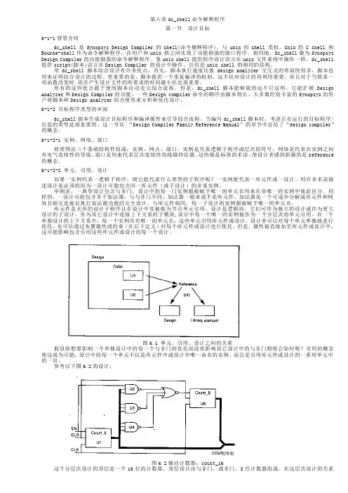
第六章dc_shell命令解释程序第一节设计目标6-1-1背景介绍dc_shell 是Synopsys Design Compiler的shell(命令解释程序),与unix的shell 类似。
Unix的C shell 和Bourne-shell作为命令解释程序,在用户和unix 核之间实现了功能极强的接口程序。
相同地,Dc_shell最为Synopsys Design Compiler的功能极强的命令解释程序。
象unix shell 提供程序设计语言在unix 文件系统中操作一样,dc_shell 提供script(脚本)语言在Design Compiler 的设计中操作,且仿造unix shell 的相同的结构。
用dc_shell 脚本综合设计有许多优点:首先,脚本执行速度比象design analyzer 交互式的界面快得多,脚本也用来证明综合设计的过程。
更重要的是,脚本提供一个重复编译的机制,这不仅对设计的再利用重要,而且对于当要求一项函数改变时,再次产生设计文件的所要求的时间最小化也很重要。
所有的这些优点源于使用脚本自动走完综合流程。
但是,dc_shell 脚本能够做的远不只这些,它能扩展Design Analyzer和Design Compiler的功能。
一些Design compiler命令的顺序由脚本得出。
大多数经验丰富的Synopsys的用户将脚本和Design analyzer结合使用来分析和优化设计。
6-1-2 目标程序类型的审阅dc_shell脚本生成设计目标程序和编译属性来引导综合流程。
当编写dc_shell脚本时,考虑正在运行的目标程序/信息的类型是很重要的。
这一节从“Design Compiler Family Reference Manual”的章节中总结了“design compiler”的概念。
6-1-2-1 实例、网络、端口原理图由三个基础的构件组成:实例、网点、端口。
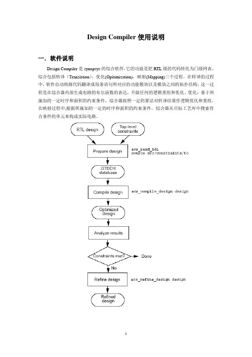
Design Compiler使用说明一.软件说明Design Compiler是synopsys的综合软件,它的功能是把RTL级的代码转化为门级网表。
综合包括转译(Translation),优化(Opitimization),映射(Mapping)三个过程。
在转译的过程中,软件自动将源代码翻译成每条语句所对应的功能模块以及模块之间的拓扑结构,这一过程是在综合器内部生成电路的布尔函数的表达,不做任何的逻辑重组和优化。
优化:基于所施加的一定时序和面积的约束条件,综合器按照一定的算法对转译结果作逻辑优化和重组。
在映射过程中,根据所施加的一定的时序和面积的约束条件,综合器从目标工艺库中搜索符合条件的单元来构成实际电路。
DC有两种界面,图形界面通过敲入design vision&调用出来,另一种命令行界面通过dc_shell-t调用。
建议初学者使用图形界面,因为图形界面比较容易上手;业界的人士比较青睐命令行界面,因为其所耗的资源少,并且将所用的命令写成综合脚本的形式,便于查阅。
因为门级和代码级不同,代码级考虑的是理想情况,但是实际电路不是这样的,它有门级的延时,线的延时,信号的转换时间,甚至时钟信号到达各个触发器的时间不相等。
基于这些考虑,DC通过施加约束,模拟实际环境,根据实际情况得出门级网表。
因此如何适当的施加约束是DC的关键所在。
二.库的配置通过上述说明可知,DC需要通用库和工艺库的支持,DC用到的工艺库是.db或者是.lib格式的,其中.lib格式的文件是可读得,通过此文件可以了解库的详细信息,比如说工作电压,操作温度,工艺偏差等等。
.db格式的库是二进制的,不可读。
.db格式的库由.lib格式的库通过命令read_lib生成。
目标工艺库(Target_library):是指将RTL级的HDL描述到门级时所需的标准单元综合库,它是由芯片制造商(Foundry)提供的,包含了物理信息的单元模型。
dc教程(word版)第⼀章基本概念1.1 启动⽂件启动⽂件⽤来指定综合⼯具所需要的⼀些初始化信息。
DC使⽤名为“.synopsys_dc.setup”的启动⽂件,启动时,DC会以下述顺序搜索并装载相应⽬录下的启动⽂件:1)、DC的安装⽬录;2)、⽤户的home⽬录;3)、当前启动⽬录。
注意:后装载的启动⽂件中的设置将覆盖先装载的启动⽂件中的相同设置。
下⾯是⼀个DC启动⽂件的实例,它包含了⼏乎所有重要的设置,下⽂将结合该实例解释启动⽂件中各项设置的具体含义。
例1-1(⼀个DC启动⽂件):search_path= search_path + {“.”, synopsys_root + “/dw/sim_ver” }search_path= search_path + { “~/risc32/synthesis/libraries” }target_library={ tcb773stc.db }synthetic_library={dw_foundation.sldb}link_library = { “*”, dw_founda tion.sldb, tcb773stc.db }symbol_library = { tcb773s.sdb }synlib_wait_for_design_license = {"DesignWare-Foundation"}alias rt “report_timing”designer= XXXXXcompany= “ASIC Lab,Fudan Univ.”●search_path指定了综合⼯具的搜索路径。
●target_library为综合的⽬标库,它⼀般是由⽣产线提供的⼯艺相关的库。
synthetic_library是综合库,它包含了⼀些可综合的与⼯艺⽆关的IP。
dw_foundation.sldb 是Synopsys提供的名为Design Ware的综合库,它包含了基本的算术运算逻辑、控制逻辑、可综合存储器等IP,在综合是调⽤这些IP有助于提⾼电路性能和减少综合时间。
#script for Design Compiler# Language : TCL# Usage :# 1) make sure the lib in the current directory# 2) if you...#script for Design Compiler# Language : TCL# Usage :# 1) make sure the lib in the current directory# 2) if you have the file .synopsys_dc.setup,# set synopsys_dc_setup_file 1,# if not, set synopsys_dc_setup_file 0# 3) change Step 3 : Variables to what you want# Especially : top module name, clock name,# reset name, all files name, and period# 4) typing dc_shell-t -f run_72.tcl | tee -i run.log##===================================================== ===set synopsys_dc_setup_file 0#-----------------------------------------------------# Step 1 :# Setting Up path and library:# If you have edited the file .synopsys_dc.setup, then you can skip over this step#-----------------------------------------------------if { $synopsys_dc_setup_file == 0} {set search_path [list /home/chanshi/dc/library/smic /home/chanshi/dc/rfid/source /home/chanshi/dc/script]set target_library {typical.db}#set target_library {CSM35OS142_typ.db};# if you want use typical library,change to typical.db#set link_library [list {*} ram_interp_typical_syn.db ram_458_typical_syn.db typical.db] set link_library [list {*} $target_library]}#set symbol_library {csm18ic.sdb csm18io.sdb}#set synthetic_library {dw_foundation.sldb};# Design Wareset command_log_file "command.log"#-----------------------------------------------------# Step 2 :# Compile Swithes#-----------------------------------------------------#set verilogout_no_tri true ;# if inout used, tri net will be used#通过将三态(tri)逻辑声明成线网(wire)来确保网表中不会出现三态逻辑,因为一些布线工具很难读取包含tri、tran源语、assign语句的网表,对于“inout”类型的port,DC产生tri wire 语句和tran 源语,对于tri,还会产生assign语句set test_default_scan_style multiplexed_flip_flop#设置扫描链的类型,还可以通过set_scan_configuration -style来设置set link_force_case case_insensitive#设置link命令是否区分大小写,默认是check_reference,就是根据产生reference的模块格式来判断是否大小写敏感,如果是vhdl格式就是不敏感,如果是verilog就敏感define_name_rules VLSI_NET -allowed "a-zA-Z0-9_" -first_restricted "0-9_" -type net -max_length 256define_name_rules VLSI_CELL -allowed "a-zA-Z0-9_" -first_restricted "0-9_" -type cell -max_length 256define_name_rules VLSI_PORT -allowed "a-zA-Z0-9_" -first_restricted "0-9_" -type port -max_length 256define_name_rules TAN_RULE -allowed "a-zA-Z0-9_" -first_restricted "0-9_\[]" -max_length 256 -map {{{"*cell*", "mycell"}, {"*-return", "myreturn"}}};set hdlin_check_no_latch "true"#设置如果推断出锁存器,是否报warning,默认是false,即不报。
DC使用说明文件说明:在进行下面的演示时需要用到两个文件,一个是example1.v,它是描述一个电路的verilog代码,我们的目标就是用DC综合这个代码得到满足约束条件的电路网表;另一个是dc.scr,它是综合example1.v的脚本文件。
这两个文件都在/home/student1000目录下,大家把它们拷贝到自己的目录下,以备使用。
DC既可使用图形界面,也可不使用图形界面而直接运行脚本来综合电路。
一、DC图形界面的使用。
1.DC图形界面的启动1.1 打开一个终端窗口,写入命令dv –db_mode,敲入回车。
则DC图形界面启动,如下图所示红框处是DC的命令输入框,以下在图形界面上的操作都可以在命令输入框中输入相应的命令来完成。
选择Help----- Man Pages可以查看DC的联机帮助。
相应指令:man。
例:man man表示查看man命令的帮助。
man create_clock表示查看creat_clock命令的帮助。
2.设置库文件选择File---- Setup需要设置以下库文件,如下图。
相应指令:set search_path [list /tools/lib/smic25/feview_s/version1/STD/Synopsys \/tools/lib/smic25/feview_s/version1/STD/Symbol/synopsys] set target_library { smic25_ff.db }set link_library { smic25_ff.db smic25_ss.db }set symbol_library { smic25.sdb }点OK,设置完成。
3.读入verilog文件选择File--- Read在打开文件对话框中选中要打开的文件,在这里我们选中example1.v文件。
在Log框中出现successfully字样表明读入文件成功。
DC(⼀)——逻辑综合及DC介绍逻辑综合定义: 将RTL逻辑综合组成: 电路的综合⼀般分为三个步骤,分别是转化(Translation)、逻辑优化(Logic Optimizaion)和映射(Mapping)。
转化(Translation):把描述RTL级的HDL语⾔,在约束下转化成DC内部的同意⽤门级描述的电路(Generic Boolean Gates).逻辑优化(Logic Optimization):把统⼀⽤门级描述的电路进⾏优化,改善路径和门。
映射(Mapping):把优化了的统⼀门级描述。
以DC为例,DC使⽤⼯艺库将电路映射出来,得到.ddc⽂件,该⽂件包含如映射的门电路信息与⽹表,.v格式的⽹标,延时信息(sdf),⼯作约束(sdc)等信息。
.ddc中包含的⽹标是实际意义上的⽹表⽂件,.v的⽹表是⽤于进⾏后仿的⽂件。
综合过程中的约束:约束对于综合⽽⾔⾮常重要,如果不施加约束,综合⼯具会产⽣⾮优化的⽹表,⽆法满⾜要求。
综合是约束驱动(Constraint driven)的,给定的约束是综合的⽬标,约束⼀般是在对整个系统进⾏时序分析得到的,综合⼯具会对电路进⾏优化以满⾜约束的要求。
综合以时序路径为基础进⾏优化。
综合过程中时序与⾯积的关系: 下图为综合过程中时序与⾯积的关系,⾯积和延迟存在折中关系。
综合⼯具以约束为指导,在满⾜时序的情况下获得最⼩⾯积。
综合的基本流程:准备RTL代码,经过前端仿真后才能⽤于综合;定义库,设定好所需要⽤到的综合库等多种库;读⼊设计,综合⼯具读⼊RTL代码并进⾏分析;定义设计环境,设定设计的⼯作环境、端⼝的驱动和负载、线负载模型等;设置设计约束(关键),主要是定义时钟和I/O的约束,约束要适当,只有正确的约束才能得到正确的结果;设置综合策略,top-down和bottom-up两种策略,根据需求进⾏选择;优化设计,综合⼯具可以根据约束对电路进⾏优化,也可认为加⼊命令改变优化⽅法;分析和解决设计的问题,在设计综合后,根据报告分析设计中出现的问题,并修订问题;保存设计数据,综合结束后,保存各种数据以供后续布局布线使⽤(需先通过验证)。
Backend Study NotesDC综合学习笔记 ................................................................................................................................................. - 1 -一、verilog 编写........................................................................................................................................... - 1 -二、DC综合注意的地方 ............................................................................................................................. - 2 -1.在同一个电路中不能同时含有触发器和锁存器两种电路单元。
................................................. - 2 -2.在电路中不能出现有反馈的组合逻辑。
......................................................................................... - 2 -3.不能出现用一个触发器的输出作为另一个触发器的时钟。
......................................................... - 2 -4.异步逻辑和模拟电路要单独处理。
................................................................................................. - 2 -5.使用的单元电路没有映射到工艺库中。
DC综合全过程及使用的命令DC的初始化文件.synopsys.dc.setup,该文件是隐藏文件,需要用ls –a显示读取文件DC支持多种硬件描述格式,.db .v .vhd等对于dcsh工作模式来说,读取不同的文件格式需要不同的参数Read -format Verilog[db\vhdl ect] file //dcsh工作模式对于tcl工作模式来说,读取不同文件格式使用不同的命令。
Read_db file.db //tcl工作模式读取db格式Read_verilog file.v //tcl工作模式读取verilog格式Read_vhdl file.v //tcl工作模式读取vhdl格式读取源程序的另外一种方式是配合使用analyzer命令和elaborate命令;Analyzer是分析HDL的源程序并将分析产生的中间文件存于work(用户可以自己指定)的目录下Elaborate则在产生的中间文件中生成verilog的模块或者VHDL的实体缺省情况下,elaborate读取的是work目录中的文件当读取完所要综合的模块后,需要使用link命令将读到DC存储区中的模块或实体连接起来注意:如果在使用link命令后,出现unresolved design reference的警告信息,需要重新读取该模块,或者在.synopsys_dc.setup 文件中添加link_library,告诉DC到库中去找这些模块,同时还要注意search_path中的路径是否指向该模块或单元电路所在的目录Link命令执行后,DC就将模块按照RTL级或者门级的描述将电路连接起来,之后的各种限制条件就可以对该电路的顶层模块施加DC限制条件施加的对象针对以下电路成分:输入输出端口、模块、子模块的实例化、单元电路、连线及电路的引脚。
在使用DC命令的时候,不要使用模糊的对象,例如,如下面的电路:Set_load 3 Clk由于在电路中含有名称为CLK的pin、port和net,因此,DC无法知道该处的load是施加在哪个对象上,注意到一般连线会驱动负载,该命令就改为:Set_load 3 [get_nets Clk] TCL modeSet_load 3 find(net,”Clk”)dc_shell mode路径的划分与合法路径DC综合的时候是基于路径的优化,对于DC来说,合法的路径必须满足以下条件路径的起点为输入端口或者是触发器的数据端路径终点为输出端口或者是触发器的时钟端DC设定的限制条件的值都是无单位的,这些单位都是由工艺库中给定的可以用report_lib lib_name来查看所有在工艺库中设定的各个参数的单位定义电路的工作环境和综合环境1.Set_operating_conditions不同的工作环境对应的单元电路的延迟不相同温度升高、电压降低、电路的特征线宽增大都会使得单元电路的延迟增大电路的工作环境一般在工艺库中都有给定命令格式:set_operating_conditions [–min min_condition] [–max max_condition] [-min_library min_lib] [–max_library max_lib]命令使用说明指定DC进行优化时使用的工作环境,其中工作环境的指定必须在库中指定,或者在link_library中的其中一个库中指定,如果不指定operating_conditions,DC自动搜索link_library中的第一个库的工作环境作为优化时使用的工作环境可以用get_attributes语句取得库中缺省的工作环境-max选项指定电路最大延迟分析(分析电路是否满足触发器建立时间set up的要求)的工作环境-min选项用于指定电路最小延迟分析(分析电路是否满足触发器保持时间hold time的要求)的工作环境,该选项不能单独使用,必须与-max同时使用如果不指定用于分析最小延迟的库,则只使用-max中指定的库用于电路的延迟分析-min_library选项指定用于电路最大延迟分析的工艺库-max_library选项指定用于电路最小延迟分析的工艺库2.set_min_libraryVendor可能提供多个不同的工艺库,用于分析电路的时序,不同工艺库定义了不同的工作环境、不同的线负载模型、不同的单元延迟时间,这是可以将这些苦都指定用于分析电路的延迟命令格式:set_min_library max_library –min_version min_library | -none命令的使用说明:该命令指定max_library用于分析电路的最大延迟,min_library用于分析电路的最小延迟。
#script for Design Compiler# Language : TCL# Usage :# 1) make sure the lib in the current directory# 2) if you...#script for Design Compiler# Language : TCL# Usage :# 1) make sure the lib in the current directory# 2) if you have the file .synopsys_dc.setup,# set synopsys_dc_setup_file 1,# if not, set synopsys_dc_setup_file 0# 3) change Step 3 : Variables to what you want# Especially : top module name, clock name,# reset name, all files name, and period# 4) typing dc_shell-t -f run_72.tcl | tee -i run.log##===================================================== ===set synopsys_dc_setup_file 0#-----------------------------------------------------# Step 1 :# Setting Up path and library:# If you have edited the file .synopsys_dc.setup, then you can skip over this step#-----------------------------------------------------if { $synopsys_dc_setup_file == 0} {set search_path [list /home/chanshi/dc/library/smic /home/chanshi/dc/rfid/source /home/chanshi/dc/script]set target_library {typical.db}#set target_library {CSM35OS142_typ.db};# if you want use typical library,change to typical.db#set link_library [list {*} ram_interp_typical_syn.db ram_458_typical_syn.db typical.db] set link_library [list {*} $target_library]}#set symbol_library {csm18ic.sdb csm18io.sdb}#set synthetic_library {dw_foundation.sldb};# Design Wareset command_log_file "command.log"#-----------------------------------------------------# Step 2 :# Compile Swithes#-----------------------------------------------------#set verilogout_no_tri true ;# if inout used, tri net will be used#通过将三态(tri)逻辑声明成线网(wire)来确保网表中不会出现三态逻辑,因为一些布线工具很难读取包含tri、tran源语、assign语句的网表,对于“inout”类型的port,DC产生tri wire 语句和tran 源语,对于tri,还会产生assign语句set test_default_scan_style multiplexed_flip_flop#设置扫描链的类型,还可以通过set_scan_configuration -style来设置set link_force_case case_insensitive#设置link命令是否区分大小写,默认是check_reference,就是根据产生reference的模块格式来判断是否大小写敏感,如果是vhdl格式就是不敏感,如果是verilog就敏感define_name_rules VLSI_NET -allowed "a-zA-Z0-9_" -first_restricted "0-9_" -type net -max_length 256define_name_rules VLSI_CELL -allowed "a-zA-Z0-9_" -first_restricted "0-9_" -type cell -max_length 256define_name_rules VLSI_PORT -allowed "a-zA-Z0-9_" -first_restricted "0-9_" -type port -max_length 256define_name_rules TAN_RULE -allowed "a-zA-Z0-9_" -first_restricted "0-9_\[]" -max_length 256 -map {{{"*cell*", "mycell"}, {"*-return", "myreturn"}}};set hdlin_check_no_latch "true"#设置如果推断出锁存器,是否报warning,默认是false,即不报。
set hdlin_merge_nested_conditional_statements "true"#顾名思义,是否把嵌套的if融合,默认值是false,就是对于嵌套的条件语句(if或case 语句)中的每一个if和case都推断出一个选择器,这种做法有利于把某些迟到的条件判断信号(late arriving signals)安排到离输出最近的选择器上(进而有利于减小延迟),如果设成true,就会把这些选择器融合成一个大的选择器,这样所有的选择信号到输出的距离都是相同的#-----------------------------------------------------# Step 3 :# Define Variables#-----------------------------------------------------set active_design "whole_modules";# Top module namesource files.tcl;# All RTL source_files (verilog)set clock_name "clk";# Name of clockset reset_name "reset";# Name of resetset clk_period 70.0#设置时钟周期,注意带小数点,这样计算出的值都带小数点,不然小于1的数都显示为0 # Desired Clock Period = 1000/Frequenceset clk_uncertainty_setup [expr $clk_period/200];#设置时钟不确定性,这里只设置了相对于建立时间的不确定性,就是时钟上升沿有可能提前clk_uncertainty_setup(时钟偏差和时钟抖动之和)到来,dc要提前clk_uncertainty_setup 检查建立时间是否满足# Uncertainty of clockset clk_latency [expr $clk_period/10];#设置时钟延迟,是时钟信号从其实际时钟原点到设计中时钟定义点的传输时间# Network Latency of clock#考虑reg1+combo1--------combo2_input+reg2+combo2_output-----------combo3+reg3的模型来解释input_delay和output_delay,中间的combo2_input+reg2+combo2_output 是要综合的模块set input_delay [expr $clk_period/4];#设置输入延迟,设置一个外部输入(组合逻辑combo1)用了多少时间(即从时钟上升沿到输入数据到来经历的延迟),dc计算还有多少时间留给内部组合逻辑combo2_input,例如时钟周期为10ns,input_delay是4ns,则还有(6-tsu)留给内部组合逻辑combo2_input # Input Delay of all input ports except clockset output_delay [expr $clk_period/4];#设置输出延迟,设置一个外部输出(组合逻辑combo3)用了多少时间(即外部组合逻辑的延迟),dc计算有多少时间留给内部组合逻辑combo2_output,例如时钟周期为10ns,output_delay为4ns,则还有(6-Tclk2Q)留给内部组合逻辑combo2_output# Output Delay of all output portsset area_desired 0;#设置面积的期望值,用于set_max_areaset wire_load_model "smic18_wl20";#为了精确地计算设置线载模型(DC支持三种模式:以此来决定如何选择用于跨层次边界的网线的线载模型),用于计算时序路径的延迟,用于set_wire_load_model# Model of the intra netset output_load "typical/NAND2BX1/AN" ;#为了精确地计算输出电路的时间,需要设置端口负载(输出或输入的外部电容负载),就是为所有输出端口指定一个负载,综合时dc就会认为这里有一个这样的负载(并不是说综合时在这里强制添加一个电容),dc综合时就会选择满足这个负载的器件,例如假设已经知道某输出端口要驱动的是一个反相器,那么把输出负载设置成这个反相器的输入负载即可,当然可以设置成很大,这样dc就会用驱动能力很大的器件,来满足所有单元被驱动。