主流存储Scalar-out system对比
- 格式:pdf
- 大小:2.40 MB
- 文档页数:29

超融合解决方案V3.0 超融合解决方案目录第1章、前言 51.1IT时代的变革 (5)1.2白皮书总览 (7)第2章、超融合技术架构 (8)1.1超融合架构概述 (8)1.1.1超融合架构的定义 (8)1.2超融合架构组成模块 (8)1.2.1.1系统总体架构 (8)1.2.1.2aSV计算虚拟化平台 (9)1.2.1.2.1概述 (9)1.2.1.2.2aSV技术原理 (10)1.2.1.2.2.1 aSV的Hypervisor架构 (12)1.2.1.2.2.2 Hypervisor虚拟化实现 (16)1.2.1.2.3aSV的技术特性 (24)1.2.1.2.3.1 内存NUMA技术 (24)1.2.1.2.3.2 SR-IOV (25)1.2.1.2.3.3 Faik-raid (27)1.2.1.2.3.4 虚拟机生命周期管理 (28)1.2.1.2.3.5 虚拟交换机 (29)1.2.1.2.3.6 动态资源调度 (29)1.2.1.2.4aSV的特色技术 (30)1.2.1.2.4.1 快虚 (30)1.2.1.2.4.2 虚拟机热迁移 (31)1.2.1.2.4.3 虚拟磁盘加密 (32)1.2.1.2.4.4 虚拟机的HA (33)1.2.1.2.4.5 多USB映射 (34)1.2.1.3aSAN存储虚拟化 (35)1.2.1.3.1存储虚拟化概述 (35)1.2.1.3.1.1 虚拟后对存储带来的挑战 (35)1.2.1.3.1.2 分布式存储技术的发展 (36)1.2.1.3.1.3 aSAN概述 (36)1.2.1.3.2aSAN技术原理 (37)1.2.1.3.2.1 主机管理 (37)1.2.1.3.2.2 文件副本 (37)1.2.1.3.2.3 磁盘管理 (39)1.2.1.3.2.4 SSD读缓存原理 (41)1.2.1.3.2.5 SSD写缓存原理 (47)1.2.1.3.2.6 磁盘故障处理机制 (51)1.2.1.3.3aSAN功能特性 (63)1.2.1.3.3.1 存储精简配置 (63)1.2.1.3.3.2 aSAN私网链路聚合 (64)1.2.1.3.3.3 数据一致性检查 (65)1.2.1.4aNet网络虚拟化 (65)1.2.1.4.1网络虚拟化概述 (65)1.2.1.4.2aNET网络虚拟化技术原理 (66)1.2.1.4.2.1 SDN (66)1.2.1.4.2.2 NFV (67)1.2.1.4.2.3 aNet底层的实现 (68)1.2.1.4.3功能特性 (73)1.2.1.4.3.1 aSW分布式虚拟交换机 (73)1.2.1.4.3.2 aRouter (73)1.2.1.4.3.3 vAF (74)1.2.1.4.3.4 vAD (74)1.2.1.4.4aNet的特色技术 (75)1.2.1.4.4.1 网络探测功能 (75)1.2.1.4.4.2 全网流量可视 (75)1.2.1.4.4.3 所画即所得业务逻辑拓扑 (76)1.2.2超融合架构产品介绍 (76)1.2.2.1产品概述 (76)1.2.2.2产品定位 (77)第3章、超融合架构带来的核心价值 (78)1.1可靠性: (78)1.2安全性 (78)1.3灵活弹性 (78)1.4易操作性 (78)第4章、超融合架构最佳实践 (80)1.1 IT时代的变革20 世纪 90 年代,随着 Windows 的广泛使用及 Linux 服务器操作系统的出现奠定了 x86服务器的行业标准地位,然而 x86 服务器部署的增长带来了新的 IT 基础架构和运作难题,包括:基础架构利用率低、物理基础架构成本日益攀升、IT 管理成本不断提高以及对关键应用故障和灾难保护不足等问题。
存储分类存储分类 (1)1.存储分类简介 (2)2.存储解决方案分类 (2)2.1.DAS(直接式存储) (2)2.2.NAS(网络接入存储) (3)2.3.SAN(存储区域网络) (4)3.存储方案比较 (5)3.1.NAS、SAN与传统存储系统(DAS)的比较 (5)3.2.NAS与SAN得比较 (6)1.存储分类简介目前磁盘存储市场上的存储主要有以下几种分类。
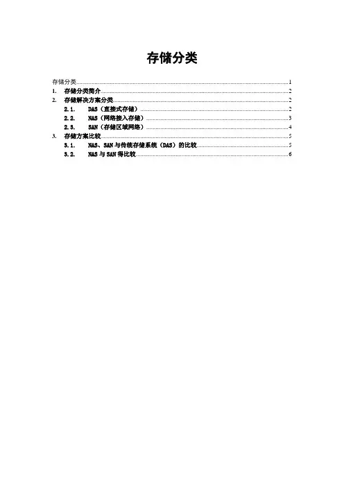
图一存储分类●存储分类根据服务器类型分为:封闭系统的存储和开放系统的存储,封闭系统主要指大型机,AS400等服务器,开放系统指基于包括Windows、UNIX、Linux等操作系统的服务器;●开放系统的存储分为:内置存储和外挂存储;●外挂存储根据连接的方式分为:直连式存储(Direct-Attached Storage,简称DAS)和网络化存储(Fabric-Attached Storage,简称FAS);●网络化存储根据传输协议又分为:网络接入存储(Network-AttachedStorage,简称NAS)和存储区域网络(Storage Area Network,简称SAN);2.存储解决方案分类绝大部分用户采用的是开放系统,其外挂存储占有目前磁盘存储市场的70%以上。
当前市场上主流的存储解决方案主要为:直连式存储(DAS)、网络接入存储(NAS)、存储区域网络(SAN)。
2.1.DAS(直接式存储)DAS(Direct Attached Storage,直接附属存储),也可称为SAS (Server-Attached Storage,服务器附加存储)。
DAS被定义为直接连接在各种服务器或客户端扩展接口下的数据存储设备,它依赖于服务器,其本身是硬件的堆叠,不带有任何存储操作系统。
在这种方式中,存储设备是通过电缆(通常是SCSI接口电缆)直接到服务器的,I/O(输入/输入)请求直接发送到存储设备。
DAS适用于以下几种环境:●服务器在地理分布上很分散,通过SAN(存储区域网络)或NAS(网络直接存储)在它们之间进行互连非常困难;●存储系统必须被直接连接到应用服务器;●包括许多数据库应用和应用服务器在内的应用,它们需要直接连接到存储器上。

了解电脑内存的类型和容量随着科技的发展,电脑已经成为了我们生活中不可或缺的重要工具。
而在电脑的硬件配置中,内存是一项至关重要的性能指标。
了解电脑内存的类型和容量对于选择适合自己需求的电脑至关重要。
本文将详细介绍电脑内存的各种类型以及容量。
一、内存类型1. DRAM(Dynamic Random Access Memory,动态随机存取存储器)DRAM是目前使用最广泛的内存类型。
它是一种易失性存储器,需要不断刷新以保持数据的完整性。
DRAM的访问速度相对较慢,但成本较低,容量较大,通常用于个人电脑和服务器。
2. SRAM(Static Random Access Memory,静态随机存取存储器)SRAM是一种高速、易失性存储器。
相比DRAM,SRAM的访问速度更快,但造价更高,容量较小。
它广泛应用于高性能计算机和缓存系统。
3. SDRAM(Synchronous Dynamic Random Access Memory,同步动态随机存取存储器)SDRAM是一种同步访问的DRAM,它的访问速度比传统的DRAM 更快。
SDRAM主要分为DDR、DDR2、DDR3和DDR4等不同的代数。
DDR4是目前市场上使用最广泛的内存类型,它的访问速度、传输带宽和能效都得到了显著的提升。
二、内存容量1. GB(Gigabyte,千兆字节)内存容量通常以GB为单位进行表示。
在选择电脑内存时,需要考虑个人使用需求和预算。
对于一般办公和上网需求,4GB或8GB的内存已经足够。
而对于高性能游戏或者专业设计软件的需求,16GB或32GB的内存可能更为适合。
2. ECC(Error-Correcting Code,纠错码)ECC内存是一种能够自动检测和纠正内存错误的高可靠性内存。
它广泛应用于服务器和工作站等对数据完整性要求较高的领域。
相比普通内存,ECC内存的价格较高,对于一般用户来说并不常见。
三、内存扩展1. DIMM(Dual In-Line Memory Module,双列直插内存模块)DIMM是目前主流的内存扩展形式之一。
热数据需要在内存中存储和处理,因此适合用缓存或内存数据库(如Redis 或SAP Hana)。
AWS提供了ElastiCache服务,可生成托管的Redis或Memcached环境。
NoSQL数据库是面向高速但小规模记录(例如,用户会话信息或物联网数据)的理想选择。
NoSQL数据库对于内容管理也很有用,可以存储数据目录。
01结构化数据存储结构化数据存储已经存在了几十年,是人们最熟悉的数据存储技术。
大多数事务型数据库(如Oracle、MySQL、SQL Server和PostgreSQL)都是行式数据库,因为要处理来自软件应用程序的频繁数据写入。
企业经常将事务型数据库同时用于报表,在这种情况下,需要频繁读取数据,但数据写入频率要低得多。
随着数据读取的需求越来越强,有更多的创新进入了结构化数据存储的查询领域,比如列式文件格式的创新,它有助于提高数据读取性能,满足分析需求。
基于行的格式将数据以行的形式存储在文件中。
基于行的写入方式是将数据写入磁盘的最快方式,但它不一定能最快地读取,因为你必须跳过很多不相关的数据。
基于列的格式将所有的列值一起存储在文件中。
这样会带来更好的压缩效果,因为相同的数据类型现在被归为一组。
通常,它还能提供更好的读取性能,因为你可以跳过不需要的列。
我们来看结构化数据存储的常见选择。
例如,你需要从订单表中查询某个月的销售总数,但该表有50列。
在基于行的架构中,查询时会扫描整个表的50个列,但在列式架构中,查询时只会扫描订单销售列,因而提高了数据查询性能。
我们再来详细介绍关系型数据库,重点介绍事务数据和数据仓库处理数据分析的需求。
(1)关系型数据库RDBMS比较适合在线事务处理(OLTP)应用。
流行的关系型数据库有Oracle、MSSQL、MariaDB、PostgreSQL等。
其中一些传统数据库已经存在了几十年。
许多应用,包括电子商务、银行业务和酒店预订,都是由关系型数据库支持的。

磁盘阵列服务器及存储解决方案服务器及存储解决方案目录前言 ..................................................................... (3)第一章需求分析 ..................................................................... (4)(一)、系统现状 ..................................................................... . (4)(二)、需求分析 ..................................................................... . (4)(三)、方案设计原则 ..................................................................... .. (4)(四)、方案概述 ..................................................................... ........................................ 5 第二章存储解决方案 ..................................................................... .. (7)(一)、采用UIT SV1600磁盘阵列的理由 (7)内置阵列卡技术和外置独立磁盘阵列技术比较 (7)UIT SV1600磁盘阵列系统 ..................................................................... .................... 9 第三章售后服务承诺 ..................................................................... (29)前言随着计算机信息管理系统的广泛应用,给人民的生产和生活带来了极大的方便。

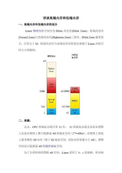
详谈高端内存和低端内存一、高端内存和低端内存的划分Linux物理内存空间分为DMA内存区(DMA Zone)、低端内存区(Normal Zone)与高端内存区(Highmem Zone)三部分。
DMA Zone通常很小,只有几十M,低端内存区与高端内存区的划分来源于Linux内核空间大小的限制。
二、来源:过去,CPU的地址总线只有32位,32的地址总线无论是从逻辑上还是从物理上都只能描述4G的地址空间(232=4Gbit),在物理上理论上最多拥有4G内存(除了IO地址空间,实际内存容量小于4G),逻辑空间也只能描述4G的线性地址空间。
为了合理的利用逻辑4G空间,Linux采用了3:1的策略,即内核占用1G的线性地址空间,用户占用3G的线性地址空间。
所以用户进程的地址范围从0~3G,内核地址范围从3G~4G,也就是说,内核空间只有1G的逻辑线性地址空间。
如果Linux物理内存小于1G的空间,通常内核把物理内存与其地址空间做了线性映射,也就是一一映射,这样可以提高访问速度。
但是,当Linux物理内存超过1G时,线性访问机制就不够用了,因为只能有1G的内存可以被映射,剩余的物理内存无法被内核管理,所以,为了解决这一问题,Linux把内核地址分为线性区和非线性区两部分,线性区规定最大为896M,剩下的128M为非线性区。
从而,线性区映射的物理内存成为低端内存,剩下的物理内存被成为高端内存。
与线性区不同,非线性区不会提前进行内存映射,而是在使用时动态映射。
三、例子假设物理内存为2G,则低段的896M为低端内存,通过线性映射给内核使用,其他的1128M物理内存为高端内存,可以被内核的非线性区使用。
由于要使用128M非线性区来管理超过1G的高端内存,所以通常都不会映射,只有使用时才使kmap映射,使用完后要尽快用kunmap释放。
对于物理内存为1G的内核,系统不会真的分配896M给线性空间,896M最大限制。
EMC/HDS/IBM三款高端存储之结构对比作者:piner (转载请注明本文出处:)永久链接:/html/y2007/m05/98-storage-contrast.html我在前面介绍了现在比较流行的三款高端存储的基本体系结构,包括IBM 的ds8000系列,hds的usp系列以及EMC的dmx3系列。
我在这里将三款高端存储再做一个简单的对比。
1、体系结构hds与emc都采用了多点冗余的复合式体系结构,有多个专用的存储控制器,如专用的前端控制器,专用的后端控制器,并且以以专用的cache 控制器为核心,CPU集成在前/后端控制器中,操作系统以微码方式集成在硬件中,并可以方便的升级维护。
在这种结构中,前端,cache,后端均可实现系统均衡,并多点冗余。
所以,失败一个点的时候,影响量比较小。
不过,还有一点差别的是,hds前后端连接到核心cache,是采用交换方式,而EMC是采用直连方式,所以也叫直连矩阵。
至于IBM,采用的是传统的对称体系结构,采用其强大的570 pserver作为存储的控制器,所以,存储的管理OS运行在控制器内,CPU与内存也都在控制器内。
这一种体系结构是应当是说与现有的中端存储的结构很相似,IBM的这种方式的体系结构在可靠性方面是比上面的体系结构要欠缺一些的。
2、后端连接与RAIDIBM采用交换方式连接磁盘与后段卡,而HDS与EMC采用环路结构,在交换结构中,每个磁盘都有自己的线路连接到后端卡(口),所以,不容易产生后端瓶颈。
至于环路设计,则是现在的流行设计,但是,一个环路上的盘不能太多,否则,容易产生性能瓶颈。
如,一个2Gb的光纤环路,一般接到50-60颗盘,已经都达到负载极限了。
而一个4Gb的环路,如果考虑翻倍的话,也就最多可以接100-120颗磁盘。
不过,上面评估磁盘个数的时候,是根据流量,也就是带宽来考虑的,如果在OLTP环境中,我们还需要考虑IO个数,因为光纤通信的规则,在同一个时间,一个环路中只能有一个通信量,也就是一个IO。
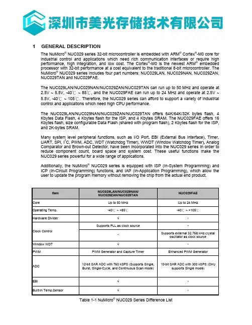
1 GENERAL DESCRIPTIONThe NuMicro® NUC029 series 32-bit microcontroller is embedded with ARM® Cortex®-M0 core for industrial control and applications which need rich communication interfaces or require high performance, high integration, and low cost. The Cortex®-M0 is the newest ARM®embedded processor with 32-bit performance at a cost equivalent to the traditional 8-bit microcontroller. The NuMicro® NUC029 series includes four part numbers: NUC029LAN, NUC029NAN, NUC029ZAN, NUC029TAN and NUC029FAE.The NUC029LAN/NUC029NAN/NUC029ZAN/NUC029TAN can run up to 50MHz and operate at2.5V ~ 5.5V, -40℃ ~ 85℃, and the NUC029FAE can run up to 24 MHz and operate at 2.5V ~5.5V, -40℃ ~ 105℃. Therefore, the NUC029 series can afford to support a variety of industrialcontrol and applications which need high CPU performance.The NUC029LAN/NUC029NAN/NUC029ZAN/NUC029TAN offers 64K/64K/32K bytes flash, 4 Kbytes Data Flash, 4 Kbytes flash for the ISP, and 4 Kbytes SRAM. The NUC029FAE offers 16 Kbytes flash, size configurable Data Flash (shared with program flash), 2 Kbytes flash for the ISP, and 2K-bytes SRAM.Many system level peripheral functions, such as I/O Port, EBI (External Bus Interface), Timer, UART, SPI, I2C, PWM, ADC, WDT (Watchdog Timer), WWDT (Window Watchdog Timer), Analog Comparator and Brown-out Detector, have been incorporated into the NUC029 series in order to reduce component count, board space and system cost. These useful functions make the NUC029 series powerful for a wide range of applications.Additionally, the NuMicro®NUC029 series is equipped with ISP (In-System Programming) and ICP (In-Circuit Programming) functions, and IAP (In-Application Programming), which allow the user to update the program memory without removing the chip from the actual end product.Table 1-1 NuMicro® NUC029 Series Difference List2 FEATURES∙ARM® Cortex®-M0 core–Runs up to 50 MHz–One 24-bit system timer–Supports Low Power Sleep mode– A single-cycle 32-bit hardware multiplier–NVIC for the 32 interrupt inputs, each with 4-levels of priority–Supports Serial Wire Debug (SWD) interface and two watchpoints/four breakpoints–Provides hardware divider and supports signed 32-bit dividend, 16-bit divisor operation(NUC029xAN only)∙Operating voltage ranges from 2.5 V to 5.5 V∙Memory–16/32/64 KB Flash for program memory (APROM)–Up to 4 KB Flash for loader (LDROM)–Up to 4 KB SRAM for internal scratch-pad RAM (SRAM)– 4 KB Flash for data memory (Data Flash) (NUC029xAN only)–Configurable Data Flash (NUC029FAE only)∙Clock Control–Programmable system clock source–22.1184 MHz internal oscillator◆Dynamically calibrating the HIRC OSC to 22.1184 MHz ±3% from -40℃ to 105℃by external 32.768 kHz crystal oscillator (LXT) (NUC029FAE only)–4~24 MHz external crystal input–10 kHz low-power oscillator for Watchdog Timer and wake-up in Sleep mode–PLL allows CPU operation up to the maximum 50 MHz (NUC029xAN only)–32.768 kHz external crystal input (LXT) for Power-down wake-up and system operation clock (NUC029FAE only)∙GPIO–Up to 40 general-purpose I/O (GPIO) pins for LQFP/QFN 48-pin package–Four I/O modes:◆Quasi-bidirectional◆Push-pull output◆Open-drain output◆Input only with high impendence–TTL/Schmitt trigger input selectable–I/O pin can be configured as interrupt source with edge/level setting–Supports high driver and high sink I/O mode–Configurable I/O mode after POR∙Timer–Up to four sets of 32-bit timers with 24-bit up counter and one 8-bit prescale counter–Independent clock source for each timer–Provides up to four timer counting modes: one-shot, periodic, toggle and continuous counting–24-bit up counter value is readable through TDR (Timer Data Register)–Supports event counting function to count the input event from external counter pin–24-bit capture value is readable through TCAP (Timer Capture Data Register)–Supports external capture pin for interval measurement◆Supports external capture pin to reset 24-bit up counter◆Supports chip wake-up from Idle/Power-down mode if a timer interrupt signal isgenerated–Supports internal capture triggered while internal ACMP output signal transition(NUC029xAN only)–Supports Inter-Timer trigger mode (NUC029xAN only)–Supports internal signal (CPO0, CPO1) for interval measurement (NUC029FAE only)∙WDT (Watchdog Timer)–Multiple clock sources–Supports wake-up from Power-down or Sleep mode–Interrupt or reset selectable on watchdog time-out–Time-out reset delay period can be selected to 3/18/130/1026 * WDT_CLK (NUC029xAN only)∙WWDT (Window Watchdog Timer) (NUC029xAN only)–6-bit down counter with 11-bit pre-scale for wide range window selected∙PWM Generator and Capture Timer (NUC029xAN only)–Up to four built-in 16-bit PWM generators, providing eight PWM outputs or four complementary paired PWM outputs–Individual clock source, clock divider, 8-bit pre-scalar and dead-zone generator for each PWM generator–PWM interrupt synchronized to PWM period–16-bit digital Capture timers with rising/falling capture inputs–Supports capture interrupt–Internal 10 kHz to PWM clock source–Polar inverse function–Center-aligned type function–Timer duty interrupt enable function–Two kinds of PWM interrupt period type selection–Two kinds of PWM interrupt duty type selection–Period/duty trigger ADC function–PWM Timer synchronous start function∙Enhanced PWM Generator (NUC029FAE only)–Independent 16-bit PWM duty control units with maximum three outputs–Supports group/synchronous/independent/ complementary modes–Supports One-shot or Auto-reload mode–Supports Edge-aligned and Center-aligned type–Programmable dead-zone insertion between complementary channels–Each output has independent polarity setting control–Hardware fault brake protections–Supports duty, period, and fault break interrupts–Supports duty/period trigger ADC conversion–Timer comparing matching event trigger PWM to do phase change–Supports comparator event trigger PWM to force PWM output low for current period –Provides interrupt accumulation function∙UART–Up to two sets of UART devices–Programmable baud-rate generator–Buffered receiver and transmitter, each with 16 bytes FIFO–Optional flow control function (CTS and RTS)–Supports IrDA(SIR) function–Supports RS-485 function–Supports LIN function (NUC029xAN only)∙SPI–Up to two sets of SPI devices–Supports Master/Slave mode–Full-duplex synchronous serial data transfer–Provides 3 wire function–Variable length of transfer data from 8 to 32 bits–MSB or LSB first data transfer–Rx latching data can be either at rising edge or at falling edge of serial clock–Tx sending data can be either at rising edge or at falling edge of serial clock–Supports Byte Suspend mode in 32-bit transmission–4-level depth FIFO buffer–PLL clock source (NUC029xAN only)∙I2C–Up to two sets of I2C modules–Supports Master/Slave mode–Bi-directional data transfer between masters and slaves–Multi-master bus (no central master)–Arbitration between simultaneously transmitting masters without corruption of serial data on the bus–Serial clock synchronization allows devices with different bit rates to communicate via one serial bus–Serial clock synchronization can be used as a handshake mechanism to suspend and resume serial transfer–Programmable clocks allow versatile rate control–Supports 7-bit addressing mode–Supports multiple address recognition (four slave addresses with mask option)–Supports Power-down wake-up function–Supports FIFO function (NUC029FAE only)∙ADC–12-bit SAR ADC with 760 kSPS for NUC029xAN, and 10-bit SAR ADC with 300 kSPS for NUC029FAE–Up to eight single-end analog input channels◆Or four differential analog input channels (NUC029xAN only)–Four operation modes (NUC029FAE only support Single mode)◆Single mode: A/D conversion is performed one time on a specified channel◆Burst mode: A/D converter samples and converts the specified single channeland sequentially stores the result in FIFO◆Single-cycle Scan mode: A/D conversion is performed only one cycle on allspecified channels with the sequence from the smallest numbered channel tothe largest numbered channel◆Continuous Scan mode: A/D converter continuously performs Single-cycle Scanmode until software stops A/D conversion–An A/D conversion can be started by:◆Software Write 1 to ADST bit◆External pin (STADC)◆PWM trigger with optional start delay period–Each conversion result is held in data register with valid and overrun indicators–Each channel has individual data register (NUC029xAN only)–Conversion result can be compared with specified value and user can select whether to generate an interrupt when conversion result matches the compare register setting –Internal temperature sensor output (NUC029xAN only)∙Analog Comparator–Up to four sets of Comparator analog modules–External input or internal band-gap voltage selectable at negative node–Interrupt when compared results change–Power-down wake-up∙EBI (External Bus Interface) for external memory-mapped device access (NUC029LAN/ NUC029NAN only)–Accessible space: 64 KB in 8-bit mode or 128 KB in 16-bit mode–Supports 8-bit or 16-bit data width–Supports byte-write in 16-bit data width∙ISP (In-System Programming) and ICP (In-Circuit Programming)∙IAP (In-Application Programming)∙One built-in temperature sensor with 1℃ resolution (NUC029xAN only)∙BOD (Brown-out Detector)–With 4 levels: 4.4V/3.7V/2.7V/2.2V–Supports Brown-out interrupt and reset option∙96-bit unique ID (UID)∙LVR (Low Voltage Reset)–Threshold voltage level: 2.0V∙Operating Temperature:–NUC029LAN/NUC029NAN/NUC029ZAN/NUC029TAN: -40℃~85℃–NUC029FAE:-40℃~105℃∙Reliability: EFT > ± 4 KV, ESD HBM pass 4 KV∙Packages:–All Green package (RoHS)–48-pin LQFP, 48-pin QFN, 33-pin QFN, 20-pin TSSOP。

海康威视视频云存储解决方案正文目录第一章概述.............................................1.1 系统简介........................................1.2 设计原则........................................1.3 设计目标........................................1.4 术语及缩略语解释................................1.4.1 术语解释 (8)1.4.2 英文/缩略语解释............................. 第二章总体设计.........................................2.1 需求说明........................................2.1.1 功能性需求说明..............................2.1.2 非功能性需求说明............................2.2 技术路线........................................2.3 逻辑架构........................................2.4 系统特点........................................2.4.1 高效灵活的空间管理..........................2.4.2 海量数据的快速检索..........................2.4.3 持续可靠的数据服务..........................2.4.4 高可扩展的应用支撑..........................2.4.5 开放透明的兼容系统......... 错误!未指定书签。
常见服务器储存类型在当今数字化的时代,服务器存储对于企业和组织的运营至关重要。
无论是存储大量的数据文件,还是保障关键业务系统的稳定运行,选择合适的服务器存储类型是一项关键决策。
接下来,让我们一起了解一下常见的服务器存储类型。
首先要提到的是直接附加存储(DAS)。
这是一种较为简单和直接的存储方式,将存储设备(如硬盘驱动器、磁带机等)直接连接到服务器上。
它就像是服务器的“私人仓库”,只为这一台服务器服务。
DAS 的优点在于数据传输速度快,因为没有中间的网络环节来减缓数据传输。
但它的缺点也很明显,扩展性较差,如果服务器需要更多的存储空间,添加新的存储设备可能会比较麻烦,而且不同服务器之间的存储资源也无法共享。
网络附加存储(NAS)则是一种通过网络连接的存储解决方案。
它就像是一个“共享仓库”,多个服务器可以通过网络访问和共享其中的存储资源。
NAS 通常基于文件级别进行数据存储和访问,这意味着用户可以像访问本地文件系统一样访问 NAS 上的文件。
对于需要共享文件的企业环境,如文件服务器、多媒体存储等,NAS 是一个不错的选择。
它的优点是易于安装和管理,成本相对较低,并且能够提供较好的数据共享和访问性能。
不过,NAS 在处理大量并发请求时,性能可能会受到一定影响。
存储区域网络(SAN)是一种更为高端和复杂的存储架构。
SAN 不是通过普通的网络连接,而是通过专门的光纤通道或 iSCSI 等高速网络技术,将存储设备与服务器连接起来。
它就像是一个“高速物流通道”,能够为服务器提供快速、可靠的存储访问。
SAN 基于块级别进行数据存储和访问,这使得服务器可以直接将 SAN 中的存储空间视为本地磁盘,从而获得更高的性能和灵活性。
SAN 非常适合对性能和可靠性要求极高的企业关键业务应用,如数据库服务器、虚拟化环境等。
但 SAN 的部署和管理成本较高,需要专业的技术人员进行维护。
接下来是固态硬盘(SSD)存储。
与传统的机械硬盘(HDD)不同,SSD 没有机械部件,而是使用闪存芯片来存储数据。
常用内存数据库介绍随着互联网和大数据的快速发展,传统的磁盘数据库在处理大规模数据时面临着性能瓶颈。
相比之下,内存数据库因其高性能、低延迟和高并发性能等优势,正在成为许多企业和组织中的首选。
本文将介绍几种常用的内存数据库及其特点。
1. RedisRedis是一个开源的内存数据库,它支持键值存储模型,并提供了丰富的数据结构,如字符串、哈希表、列表、集合和有序集合等。
Redis以其快速的读写速度、持久化能力和高扩展性而闻名。
它可以通过持久化机制将数据保存到磁盘,以克服内存大小的限制。
此外,Redis还支持发布/订阅和事务等功能,使其成为构建缓存、会话管理、消息队列和实时分析等应用的理想选择。
2. MemcachedMemcached是一个开源的高性能分布式内存对象缓存系统。
它可以将数据存储在内存中,并提供简单、快速的键值存储访问接口。
Memcached使用键值对的方式存储数据,支持多线程并发访问,可以通过增加服务器的数量来扩展性能。
在互联网应用中,Memcached通常用于减轻数据库的负载,提高应用性能。
3. Apache IgniteApache Ignite是一个内存计算平台,它提供了分布式的内存数据库、缓存和计算引擎。
Ignite将数据存储在内存中,以实现极高的读写性能和低延迟。
它支持多种数据模型,如键值存储、关系型存储和对象存储,可以处理大规模数据和复杂查询。
此外,Ignite还提供了分布式查询、事务处理和机器学习等功能,使其成为构建实时分析、推荐系统和流式处理等应用的首选。
4. AerospikeAerospike是一个高性能的内存和闪存数据库,它专注于处理大规模的实时数据。
Aerospike使用内存和闪存的组合存储,可以实现低延迟的读写操作。
它支持键值存储和部分索引,可以处理高并发访问和大规模数据集。
Aerospike还提供了数据持久化、自动故障恢复和可扩展性等功能,适用于处理实时广告、个性化推荐和物联网等场景。
服务器存储基础知识第一点:服务器存储的类型与特点服务器存储是计算机网络中至关重要的组成部分,它负责数据的存放、管理和访问。
在服务器存储的世界里,有多种存储类型,每一种都有其独特的特点和适用场景。
1.1 直接附加存储(DAS)直接附加存储是最常见的存储类型,它将存储设备直接连接到服务器上。
这种存储类型的特点是速度快、控制简单,但扩展性和容错能力较差。
DAS适用于小型企业或者对数据访问速度有较高要求的环境。
1.2 网络附加存储(NAS)网络附加存储是通过网络连接的独立存储设备,它可以被网络中的多个服务器访问。
NAS的优点在于易于扩展和共享,但相对DAS,其访问速度可能会慢一些。
NAS适用于需要数据共享和备份的中型企业。
1.3 存储区域网络(SAN)存储区域网络是一种高速专用网络,连接服务器和存储设备。
SAN提供高效的存储池化,可以实现大量的数据存储和快速的访问速度。
但SAN的成本较高,且需要复杂的配置和管理。
它适用于大型企业或数据中心,特别是在需要高可用性和高扩展性的环境中。
1.4 分布式存储分布式存储是将存储资源分布在网络中的多个位置,通过软件进行管理和协调。
这种存储类型的优点在于高可用性和弹性,可以动态调整资源。
分布式存储适用于云计算和大数据应用,能够提供海量数据的存储和处理能力。
第二点:服务器存储的关键技术在服务器存储的领域,有一些关键技术是确保数据安全、提高数据访问效率和实现高效管理的关键。
2.1 数据冗余技术数据冗余是通过将数据复制到多个位置来提高数据的可靠性。
常见的数据冗余技术包括磁盘镜像、磁盘阵列和数据校验技术。
通过冗余技术,即使部分存储设备损坏,也不会丢失数据,提高了数据的可靠性。
2.2 数据快照技术数据快照技术可以创建数据的静态视图,使得用户可以随时访问某个时间点的数据状态。
快照可以用于数据备份、恢复和测试,大大提高了数据管理的灵活性和效率。
2.3 数据压缩和去重技术数据压缩和去重技术是为了提高存储效率而开发的。
第一章(计算机系统概论)digital computer 数字计算机decimal digits 十进制数字binary 二进制bit 位ASCII 美国国家信息交换标准代码computer system 计算机系统hardware system 硬件系统software system 软件系统I/O devices 输入输出设备central processing unit(CPU) 中央处理器memory 存储器application software 应用软件video game 计算机游戏system software 系统软件register 寄存器floating point data浮点数据Boolean布尔值character data字符数据EBCDIC扩充的二十一进制交换代码punched cards穿孔卡片magnetic tape磁带main memory主存vacuum tubes电子管magnetic drum磁鼓transistors晶体管solid-state devices固体器件magnetic cores磁芯integrated circuit(IC)集成电路silicon chip硅芯片multiprogramming多道程序设计timessharing分时分时技术minicomputers小型计算机mainframe大型计算机large-scaleintegrated(LSI)大规模集成very-large-scale integrated(VLSI)超大规模集成word processing文字处理eletronic spreedsheets电子表格database management programs数据库管理程序desktop publishing桌面印刷personalcomputer(PC)个人计算机microcomputer微型计算机storage capacities存储容量stand-alone computer独立计算机local area network(LAN)局域网peripheral devices外部设备assembly line流水线supercomputer巨型计算机第二章(计算机系统结构)memmory subsystem存储子系统I/O subsystem输入输出子系统bus总线system bus系统总线chip 芯片address bus地址总线instructions指令memory location存储单元data bus数据总线control bus控制总线local bus 局部总线microprocessor微处理器register set寄存器组arithmetic logic unit(ALU)运算器clock cycle时钟周期control unit控制器computer architecture计算机体系结构introduction format指令格式addressing modes寻址方式introduction set指令集internal memory内存main memory主存Random Access Memory(RAM)随机存取存储器Read Only Memory (ROM)只读存储器secondary storage副主存储器vitual memory虚拟存储器Dynamic RAM(DRAM)动态存储器refresh circuitry刷新电路Static RAM(SRAM)静态RAMcache memory高速缓冲存储器masked ROM掩膜ROMPROM可编程RAMEPROM可擦写PROMultraviolet light紫外线EEPROM or EEPROM电擦写PROMbasic input/output system(BIOS)基本输入输出系统flash EEPROM 快闪存储器memory hierarchy 存储器体系结构auxiliary memory 辅助存储器storage memory 存储容量keyboard 键盘alphanumeric key字母数字键function key 功能键cursor key 光标键numeric keypad 数字键mouse 鼠标touch screen触屏infrared ray红外线monitor 监视器display screen显示屏laser printer激光打印机ink-jet printer喷墨打印机dot-matrix printer点针式打印机modem调制解调器input-output interface(I/O interface)输入输出接口peripheral外部设备,外设interrupt中断program counter程序计数器vectored interrupt向量中断nonvectored interrupt非向量中断interrupt vector中断向量Direct Memory Acess(DMA)直接存储器存取timeout超时第三单元(计算机体系结构)parallel processing 并行操作serial operations 串行操作instructions stream 指令流data dream 数据流SISD 单指令单数据流SIMD 单指令多数据流MISD 多指令单数据流MIMD 多指令多数据流pipeline processing 流水线处理combinational circuit 组合电路multiplier 乘法器adder 加法器clock pulse 时钟脉冲vector processing 向量处理one-dimensional array 一维数组scalar processer 标量处理器vector instructions 向量指令CISC 复杂指令集计算机decoder 译码器RISC 精简指令集计算机backward compatibility 向下兼容第四单元(算法与数据结构)algorithm 算法parallel algotithm 并行算法primitive 原语syntax 语法semantics 语义pseudocode 伪码exhaustive search 穷举搜索divide-and-conquer algorithm 分治算法dynamic programming 动态规划bottom-up 自上而下top-down 自下而上array 数组one-dimensional array 一维数组pointer 指针program counter 程序计数器instruction pointer 指令指针list 列表linked list 链表singly-linked list 单向链表double-linked list 双向链表circularly-linked list 循环链表FIFO 先进先出LIFO 后进先出stack 栈push 压栈pop 出栈stack pointer 栈指针queue 队列tree 树root 根level 层次degree of a node 结点的度depth of a tree树的深度binary tree 二叉树traversal 遍历M-way search tree M向搜索树第五章(编程语言)Program 程序Program language 程序设计语言Software engineering 软件工程Pseudocode 伪码Flowchart 流程图Coding 编码Program testing 程序测试Desk-checking 手工检查Documentation 文档User documentation 用户文档Operator documentation 操作员文档Programmer documentation 程序员文档Machine language 机器语言Assembly languages 汇编语言High-level languages 高级语言RAD(rapid application development) 快速应用开发Natural language 自然语言Artificial intelligence(AI) 人工智能Compile 编译Assemble 汇编Source code 源代码Object code 目标代码Linker 连接器Executable file 可执行文件Object-oriented programming 面向对象的程序设计Object 对象Class 类ADT(abstract data type)抽象数据类型Member variable 成员变量Class variable 类变量Member function 成员函数Inheritance 继承Derived class 派生类Overload 超载Message 消息Static binding 静态绑定Dynamic binding 动态绑定Polymorphism 多态性Visual programming 可视化编程Markup language 标记语言HTML(hyper text markup language)超文本标记语言Hyperlink 超链接XML(extensible markup language) 可扩展标记语言Java virtual machine java虚拟机第六章(操作系统)Application software 应用软件System software 系统软件Utility software 实用软件Operating system(OS)操作系统Shell 操作系统的外壳程序Graphical user interface(GUI)图形用户界面Kernel 内核Serial processing 串行处理Job 作业Batch processing 批处理Simple batch systems 简单批处理系统Multiprogrammed batch systems 多道程序批处理系统Monitor 监控程序Scheduler 调度程序Multiprogramming 多道程序Multitasking 多任务Time-sharing systems 分时系统Uniprogramming 单道进程Process 进程Process management 进程管理Process control block 进程控制块Mutual exclusion 互斥Multiprocessing 多处理,多进程Distributed processing 分布式管理Concurrent processes 并发处理Deadlock 死锁Synchronize process同步处理Semaphore 信号量Reusable resource 可复用性资源I/O buffers 输入/输出缓冲区I/O channel 输入/输出通道Deadlock prevention 死锁预防Deadlock detection 死锁检测Deadlock avoidance 死锁避免Virtual memory 虚拟内存Logical reference 逻辑引用Real addresse 实地址Paging 分页Segmentation 分段Virtual address 虚拟地址Physical addresses 物理地址Real-time process 实时处理File management 文件管理Plug and play(PnP) 即插即用第七单元(应用软件)application software 应用软件word processing 字处理软件spreadsheet 电子表格personal finance 个人理财presentation graphic 演示图形database manager 数据库管理软件groupware 群件desktop accessory 桌面辅助工具browsers 浏览区desktop publishing 桌面印刷project management 项目管理CAD 计算机辅助设计CAM 计算机辅助制造multimedia authoring 多媒体发布animation 动画MIDI 乐器数字化接口speech synthesis 语音合成insertion point 插入点scroll bar 滚动条window 窗口menu bar 菜单栏pull-down menu 下拉式菜单Button 按钮toolbar 工具条dialog box 对话框default value 缺省值(默认值)macro 宏OLE 对象链接和嵌入clipboard 剪切板column 列row 行cell 单元格cell address 单元格地址cell pointer 单元格指针formula 公式function 函数bar chart 柱形图line chart 线图pie chart 圆饼图workflow software 工作流软件PIM 个人信息管理软件Web browser 浏览器World Wide Web 万维网home page 主页第八单元(数据库)DBMS 数据库管理系统instance 实例schema 模式physical schema 物理模式存储模式内模式logical schema 逻辑模式概念模式模式subschema 子模式外模式data independence 数据独立性physical data independence 物理数据独立性logical data independence 逻辑数据独立性data model 数据模型entity-relationship model 实体联系模型object-oriented model 面向对象模型semantic data model 语义数据类型functional data model 功能数据模型entity 实体entity set 实体集mapping cardinality 映射基数abstract data type 抽象数据类型attribute 属性relation 关系tuple 元组primary key 主键super key 超健candidate key 候选键foreign key 外键DDL 数据定义语言data dictionary 数据字典DML 数据操纵语言procedure DML 过程化DML nonprocedure DML 非过程化DMLSQL 结构化查询语言view 视图the relational algebra 关系代数the tuple relational calculus 元组关系演算atomicity 原子性consistency 一致性duration 持久性transaction 事物DBA 数据库管理员。
大数据时代的存储和管理技术
随着大数据时代的到来,存储和管理技术也迎来了巨大的变革和挑战。
以下是一些当前比较主流的存储和管理技术:
1.分布式存储技术:分布式存储是在多个物理节点上分散存储大量数
据的一种存储方式。
通过分片技术,将大数据拆分成多份存储在不同的物
理节点上,避免了单一节点存储压力过大的问题,提高了系统的可靠性和
可扩展性。
2. NoSQL数据库技术:NoSQL数据库是指非关系型数据库,与传统的
关系型数据库相比,NoSQL具有高可用性、高可扩展性和高性能等优势,
在大数据时代得到了广泛应用。
NoSQL数据库的代表性产品包括MongoDB、Cassandra和Redis等。
3. Hadoop和Spark相关技术:Hadoop是一个开源的分布式计算框架,提供了分布式存储和分布式处理能力,是处理大数据的重要工具。
而
Spark则是一个基于内存的快速大数据处理引擎,可以与Hadoop结合使用,提高数据处理效率。
4.异构存储技术:异构存储是指将不同类型的存储设备组合在一起形
成存储池,进而实现动态存储分配和数据迁移。
通过合理地利用不同类型
存储设备的特点,可以提高存储效率和成本效益。
5.元数据管理技术:元数据是指描述数据的数据,是大数据管理的关
键之一。
元数据管理技术包括元数据采集、建模、标准化、维护和应用等
方面,可以实现数据的一体化管理和有效利用。
总之,随着大数据时代的发展,存储和管理技术会不断推陈出新,不
断为处理大数据提供更加高效、快速、精准的解决方案。