PG48FSUSC USC 规格书 KEC推荐
- 格式:pdf
- 大小:123.14 KB
- 文档页数:3

FS2100系列2.5G OC48过滤卡用户手册《FS-2100系列2.5G OC48过滤卡用户手册》 武汉飞思科技有限公司2FS4100系列2.5G OC48过滤卡用户手册资料编号 DOC- OC48PCI-UM 产品版本 V1.0 资料状态 发行版权声明© 武汉飞思科技有限公司版权所有,并保留对本手册及本声明的最终解释权和修改权。
本手册的版权归武汉飞思科技有限公司所有。
未得到武汉飞思科技有限公司的书面许可,任何人不得以任何方式或形式对本手册内的任何部分进行复制、摘录、备份、修改、传播、翻译成其它语言、将其全部或部分用于商业用途。
免责声明本手册依据现有信息制作,其内容如有更改,恕不另行通知。
武汉飞思科技有限公司在编写该手册的时候已尽最大努力保证其内容准确可靠,但武汉飞思科技有限公司不对本手册中的遗漏、不准确或错误导致的损失和损害承担责任。
使用者警示本产品是 A 级通讯产品,当在居住环境中使用时,可能会造成射频干扰,在这种情况下使用者应采取适当的对策以避免影响使用者的正常生活。
《FS-2100系列2.5G OC48过滤卡用户手册》 武汉飞思科技有限公司3手册使用说明读者对象本手册的读者对象为安装FS2100系列OC48过滤卡的工程技术人员和采用FS2100系列OC48过滤卡的软件开发人员。
本手册需要读者具有一定的网络技术知识和经验。
内容介绍本手册详细介绍了FS2100系列OC48过滤卡的安装方法,调试命令以及编程接口。
《FS2100系列OC48过滤卡用户手册》共分为六章:第1章 产品综述 详细阐述了FS2100系列OC48过滤卡的特性和产品规格。
第2章 产品硬件结构 详细阐述了FS2100系列OC48过滤卡的硬件结构和选配部件介绍。
第3章 驱动安装 详细阐述了FS2100系列OC48过滤卡在windows 和linux 下驱动和库的安装方法。
第4章 调试命令 详细阐述了FS2100系列OC48过滤卡在使用过程中的需要调试和查看状态的命令。

Product Product TypeBattery Type Recommended Battery Brand (UL/ULC approved)BatteryQTYExpectedBattery Life(with typical use)Low Battery Threshold PGx916Smoke Detector CR123A Panasonic Industrial or GPWireless1 5 years2.5V PGx926CR123A Panasonic Industrial or GPWireless1 5 years2.5V PGx936AAADuracell Procell PC2400 orEnergizer E92 batteries 3 3 years3.75V PGx913Carbon Monoxide Detector 9 Volt Alkaline battery Energizer #522, Duracell#MN1604.1 1 years7.3V PGx933CR123APanasonic Industrial 1 5 years 2.85V PGx901Indoor SirenBATT13.0-3.6V1 x customized D type battery DSC 18 years 2V PGx901 BATT BATT-PGX901/X9114 x customized A type battery DSC 18 years 2V PGx911Outdoor Siren BATT13.0-3.6V1 x customized D type battery DSC18 years2VPGx911A BATT BATT-PGX901/X9114 x customized A type battery DSC 18 years 2VPGx911B BATT PGx938Wireless Panic CR2032Varta or Panasonic Industrial 1 5 years 2.05V PGx9492-button Wireless Key CR2032Varta or Panasonic Industrial 1 5 years 2.05V PGx9394-button Wireless Key CR2032Varta or Panasonic Industrial 18 years 2.2V PGx929CR2032Varta or Panasonic Industrial1 5 years 2.1V PGx920Wireless RepeaterBATT1.3-4.8V - Rechargeablecustomized Ni-MH DSC148 hours 4.8V PGx912Wireless Glass-break Detector CR123A Panasonic or GP Wireless 1 4 years 2.7V PGx922CR123A Panasonic or GP Wireless 1 5 years 2.6V PGx924Curtain Motion Detector CR123APanasonic or GP Wireless17 years 2.45V PGx934(P)Indoor Motion Detector with cameraBATT-PGX934P -customized LI-ME C123A pack DSC14-5 years 4.5V PGx944Outdoor Motion Detector with camera BATT-PGX944 - customizedLI-ME CR17450 packDSC2 3 years 4.0V PGx994Outdoor Motion Detector CR123APanasonic Industrial orGP Wireless2 3 years 4.0V PGx904(P)Wireless PowerG PIR Security Motion DetectorCR123APanasonic Industrial orGP Wireless 16-8 years 2.5V PGx914Wireless PowerG Digital Pet-Immune PIR Motion DetectorCR123APanasonic Industrial orGP Wireless 16-8 years 2.4V PGx974(P)Wireless PowerG Mirror Optic PIR Motion DetectorCR123APanasonic Industrial orGP Wireless 17 years 2.45V PGx984(P)Wireless PowerG Dual Technology Security Motion DetectorCR123APanasonic Industrial,Varta, GP Wireless 15-7 years 2.5V PGx905Temperature Sensor CR123APanasonic Industrial orGP Wireless17 years 2.2V PGx985Flood Sensor CR123APanasonic Industrial orGP Wireless18 years 2.2V PGx935Shock Sensor CR123APanasonic Industrial orGP Wireless 1 5 years 2.6V PGx945Door/Window contact w/aux input CR123A Panasonic Industrial, GP 18 years 2.2V PGx975Vanishing Door/Window Contact CR2032Varta or Panasonic Industrial 1 3 years 2.1V PGx307Recessed Door Contact CR2Panasonic Industrial or GP Wireless110 years2.5VPGx862360° Ceiling Mount PIR DetectorCR123APanasonic Industrial or GP Wireless1minimum 1 yeartypical use 5 years2.5VProduct Battery Quick Reference Guide APAC, EMEA, LATAM, NAintrusionSecurity | Access | Video | Intrusion | Converged Solutions | ServicesIn the notation ‘PGx###’, x designates the frequency of the detector. EX. x = 4 (433MHz), 8 (868MHz)PowerG_battery-guide_ROW_v1.indd 12018-12-21 2:22 PM。
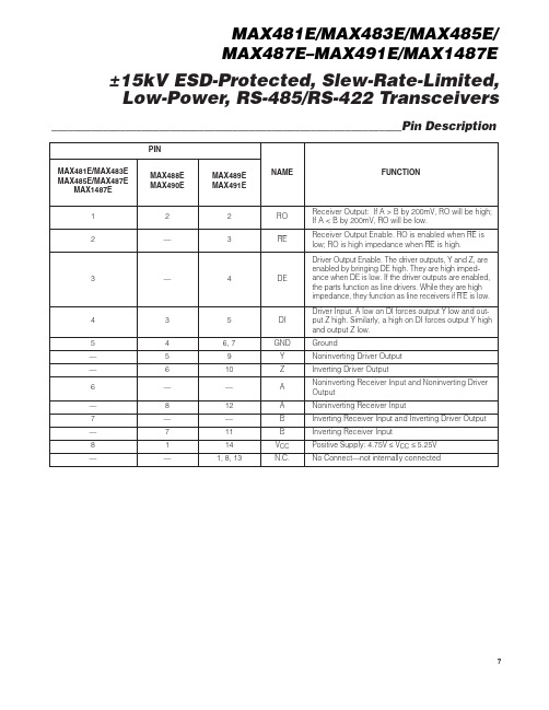
±15kV ESD-Protected, Slew-Rate-Limited,Low-Power, RS-485/RS-422 Transceivers ______________________________________________________________Pin DescriptionMAX481E/MAX483E/MAX485E/MAX487E–MAX491E/MAX1487E7±15kV ESD-Protected, Slew-Rate-Limited,Low-Power, RS-485/RS-422 Transceivers__________Function Tables (MAX481E/MAX483E/MAX485E/MAX487E/MAX1487E) Table 1. Transmitting Table 2. Receiving__________Applications Information The MAX481E/MAX483E/MAX485E/MAX487E–MAX491E and MAX1487E are low-power transceivers for RS-485 and RS-422 communications. These “E” versions of the MAX481, MAX483, MAX485, MAX487–MAX491, and MAX1487 provide extra protection against ESD. The rugged MAX481E, MAX483E, MAX485E, MAX497E–MAX491E, and MAX1487E are intended for harsh envi-ronments where high-speed communication is important. These devices eliminate the need for transient suppres-sor diodes and the associated high capacitance loading. The standard (non-“E”) MAX481, MAX483, MAX485, MAX487–MAX491, and MAX1487 are recommended for applications where cost is critical.The MAX481E, MAX485E, MAX490E, MAX491E, and MAX1487E can transmit and receive at data rates up to 2.5Mbps, while the MAX483E, MAX487E, MAX488E, and MAX489E are specified for data rates up to 250kbps. The MAX488E–MAX491E are full-duplex transceivers, while the MAX481E, MAX483E, MAX487E, and MAX1487E are half-duplex. In addition, driver-enable (DE) and receiver-enable (RE) pins are included on the MAX481E, MAX483E, MAX485E, MAX487E, MAX489E, MAX491E, and MAX1487E. When disabled, the driver and receiver outputs are high impedance.±15kV ESD Protection As with all Maxim devices, ESD-protection structures are incorporated on all pins to protect against electro-static discharges encountered during handling and assembly. The driver outputs and receiver inputs have extra protection against static electricity. Maxim’s engi-neers developed state-of-the-art structures to protect these pins against ESD of ±15kV without damage. The ESD structures withstand high ESD in all states: normal operation, shutdown, and powered down. After an ESD event, Maxim’s MAX481E, MAX483E, MAX485E, MAX487E–MAX491E, and MAX1487E keep working without latchup.ESD protection can be tested in various ways; the transmitter outputs and receiver inputs of this product family are characterized for protection to ±15kV using the Human Body Model.Other ESD test methodologies include IEC10004-2 con-tact discharge and IEC1000-4-2 air-gap discharge (for-merly IEC801-2).ESD Test Conditions ESD performance depends on a variety of conditions. Contact Maxim for a reliability report that documents test set-up, test methodology, and test results.Human Body Model F igure 4 shows the Human Body Model, and F igure 5 shows the current waveform it generates when dis-charged into a low impedance. This model consists of a 100pF capacitor charged to the ESD voltage of inter-est, which is then discharged into the test device through a 1.5kΩresistor.IEC1000-4-2 The IEC1000-4-2 standard covers ESD testing and per-formance of finished equipment; it does not specifically refer to integrated circuits (Figure 6).MAX481E/MAX483E/MAX485E/MAX487E–MAX491E/MAX1487E Maxim Integrated9。

48V电池管理系统技术规格书48V电池管理系统技术规格书⒈介绍⑴文档目的本技术规格书旨在描述48V电池管理系统的技术要求和规范,以供设计、制造和测试人员参考。
⑵范围本规格书适用于48V电池管理系统,包括系统构成、功能特性、性能参数等方面的规范。
⒉术语定义⑴ 48V电池管理系统指用于管理和控制48V电池组的系统,包括电池监测、充放电控制、温度管理等功能。
⑵电池组由多个48V电池单体组成的组合系统,用于提供电能存储和释放功能。
⒊系统构成包括电池电压监测、电流监测、温度监测等功能的模块。
⑵充放电控制模块用于控制电池组的充放电过程,包括电池充电管理和放电保护等功能。
⑶温度管理模块用于监测和控制电池组的温度,防止过热或过冷情况的发生。
⑷通信模块用于与外部系统进行数据交互,包括与能源管理系统、车载系统等的数据通信功能。
⒋功能特性⑴电池监测功能⒋⑴电池电压监测实时监测电池组的电压情况,记录历史数据并提供报警功能。
⒋⑵电流监测实时监测电池组的充放电电流,记录历史数据并提供过流保护功能。
实时监测电池组的温度情况,记录历史数据并提供过温保护功能。
⑵充放电控制功能⒋⑴电池充电管理实现对电池组的智能充电控制,包括恒流充电、恒压充电等功能。
⒋⑵放电保护对电池组进行放电保护,避免过放电过程中电池损坏。
⑶温度管理功能⒋⑴温度监测实时监测电池组的温度情况,保证电池工作在安全温度范围内。
⒋⑵温度控制根据温度变化对电池组进行控制,防止过热或过冷情况的发生。
⑷通信功能⒋⑴数据通信与能源管理系统、车载系统等外部系统进行数据通信,提供实时数据传输功能。
⒋⑵故障诊断通过与外部系统的通信,实现对电池组的故障诊断和报警功能。
⒌性能参数⑴输入电压范围: 40V~60V⑵定额输出容量: 48V,最大电流50A⑶输出电压精度: ±1%⑷整体效率: ≥95%⑸通信接口: CAN总线⑹工作温度范围: -20℃~60℃附件:⒈电池管理系统电路图⒉电池组连接方式图⒊部分原理图和PCB布局图法律名词及注释:⒈电器安全规范: 电池管理系统需符合相关电气安全规范,如IEC 62109等。

For pricing, delivery, and ordering information,please contact Maxim/Dallas Direct!at 1-888-629-4642, or visit Maxim’s website at .General DescriptionThe MAX481, MAX483, MAX485, MAX487–MAX491, and MAX1487 are low-power transceivers for RS-485 and RS-422 communication. Each part contains one driver and one receiver. The MAX483, MAX487, MAX488, and MAX489feature reduced slew-rate drivers that minimize EMI and reduce reflections caused by improperly terminated cables,thus allowing error-free data transmission up to 250kbps.The driver slew rates of the MAX481, MAX485, MAX490,MAX491, and MAX1487 are not limited, allowing them to transmit up to 2.5Mbps.These transceivers draw between 120µA and 500µA of supply current when unloaded or fully loaded with disabled drivers. Additionally, the MAX481, MAX483, and MAX487have a low-current shutdown mode in which they consume only 0.1µA. All parts operate from a single 5V supply.Drivers are short-circuit current limited and are protected against excessive power dissipation by thermal shutdown circuitry that places the driver outputs into a high-imped-ance state. The receiver input has a fail-safe feature that guarantees a logic-high output if the input is open circuit.The MAX487 and MAX1487 feature quarter-unit-load receiver input impedance, allowing up to 128 MAX487/MAX1487 transceivers on the bus. Full-duplex communi-cations are obtained using the MAX488–MAX491, while the MAX481, MAX483, MAX485, MAX487, and MAX1487are designed for half-duplex applications.________________________ApplicationsLow-Power RS-485 Transceivers Low-Power RS-422 Transceivers Level TranslatorsTransceivers for EMI-Sensitive Applications Industrial-Control Local Area Networks__Next Generation Device Features♦For Fault-Tolerant ApplicationsMAX3430: ±80V Fault-Protected, Fail-Safe, 1/4Unit Load, +3.3V, RS-485 TransceiverMAX3440E–MAX3444E: ±15kV ESD-Protected,±60V Fault-Protected, 10Mbps, Fail-Safe, RS-485/J1708 Transceivers♦For Space-Constrained ApplicationsMAX3460–MAX3464: +5V, Fail-Safe, 20Mbps,Profibus RS-485/RS-422 TransceiversMAX3362: +3.3V, High-Speed, RS-485/RS-422Transceiver in a SOT23 PackageMAX3280E–MAX3284E: ±15kV ESD-Protected,52Mbps, +3V to +5.5V, SOT23, RS-485/RS-422,True Fail-Safe ReceiversMAX3293/MAX3294/MAX3295: 20Mbps, +3.3V,SOT23, RS-855/RS-422 Transmitters ♦For Multiple Transceiver ApplicationsMAX3030E–MAX3033E: ±15kV ESD-Protected,+3.3V, Quad RS-422 Transmitters ♦For Fail-Safe ApplicationsMAX3080–MAX3089: Fail-Safe, High-Speed (10Mbps), Slew-Rate-Limited RS-485/RS-422Transceivers♦For Low-Voltage ApplicationsMAX3483E/MAX3485E/MAX3486E/MAX3488E/MAX3490E/MAX3491E: +3.3V Powered, ±15kV ESD-Protected, 12Mbps, Slew-Rate-Limited,True RS-485/RS-422 TransceiversMAX481/MAX483/MAX485/MAX487–MAX491/MAX1487Low-Power, Slew-Rate-Limited RS-485/RS-422 Transceivers______________________________________________________________Selection Table19-0122; Rev 8; 10/03Ordering Information appears at end of data sheet.M A X 481/M A X 483/M A X 485/M A X 487–M A X 491/M A X 1487Low-Power, Slew-Rate-Limited RS-485/RS-422 Transceivers 2_______________________________________________________________________________________ABSOLUTE MAXIMUM RATINGSSupply Voltage (V CC ).............................................................12V Control Input Voltage (RE , DE)...................-0.5V to (V CC + 0.5V)Driver Input Voltage (DI).............................-0.5V to (V CC + 0.5V)Driver Output Voltage (A, B)...................................-8V to +12.5V Receiver Input Voltage (A, B).................................-8V to +12.5V Receiver Output Voltage (RO).....................-0.5V to (V CC +0.5V)Continuous Power Dissipation (T A = +70°C)8-Pin Plastic DIP (derate 9.09mW/°C above +70°C)....727mW 14-Pin Plastic DIP (derate 10.00mW/°C above +70°C)..800mW 8-Pin SO (derate 5.88mW/°C above +70°C).................471mW14-Pin SO (derate 8.33mW/°C above +70°C)...............667mW 8-Pin µMAX (derate 4.1mW/°C above +70°C)..............830mW 8-Pin CERDIP (derate 8.00mW/°C above +70°C).........640mW 14-Pin CERDIP (derate 9.09mW/°C above +70°C).......727mW Operating Temperature RangesMAX4_ _C_ _/MAX1487C_ A...............................0°C to +70°C MAX4__E_ _/MAX1487E_ A.............................-40°C to +85°C MAX4__MJ_/MAX1487MJA...........................-55°C to +125°C Storage Temperature Range.............................-65°C to +160°C Lead Temperature (soldering, 10sec).............................+300°CDC ELECTRICAL CHARACTERISTICS(V CC = 5V ±5%, T A = T MIN to T MAX , unless otherwise noted.) (Notes 1, 2)Stresses beyond those listed under “Absolute Maximum Ratings” may cause permanent damage to the device. These are stress ratings only, and functional operation of the device at these or any other conditions beyond those indicated in the operational sections of the specifications is not implied. Exposure to absolute maximum rating conditions for extended periods may affect device reliability.V V IN = -7VV IN = 12V V IN = -7V V IN = 12V Input Current (A, B)I IN2V TH k Ω48-7V ≤V CM ≤12V, MAX487/MAX1487R INReceiver Input Resistance -7V ≤V CM ≤12V, all devices except MAX487/MAX1487R = 27Ω(RS-485), Figure 40.4V ≤V O ≤2.4VR = 50Ω(RS-422)I O = 4mA, V ID = -200mV I O = -4mA, V ID = 200mV V CM = 0V-7V ≤V CM ≤12V DE, DI, RE DE, DI, RE MAX487/MAX1487,DE = 0V, V CC = 0V or 5.25VDE, DI, RE R = 27Ωor 50Ω, Figure 4R = 27Ωor 50Ω, Figure 4R = 27Ωor 50Ω, Figure 4DE = 0V;V CC = 0V or 5.25V,all devices except MAX487/MAX1487CONDITIONSk Ω12µA ±1I OZRThree-State (high impedance)Output Current at ReceiverV 0.4V OL Receiver Output Low Voltage 3.5V OH Receiver Output High Voltage mV 70∆V TH Receiver Input Hysteresis V -0.20.2Receiver Differential Threshold Voltage-0.2mA 0.25mA-0.81.01.55V OD2Differential Driver Output (with load)V 2V 5V OD1Differential Driver Output (no load)µA±2I IN1Input CurrentV 0.8V IL Input Low Voltage V 2.0V IH Input High Voltage V 0.2∆V OD Change in Magnitude of Driver Common-Mode Output Voltage for Complementary Output States V 0.2∆V OD Change in Magnitude of Driver Differential Output Voltage for Complementary Output States V 3V OC Driver Common-Mode Output VoltageUNITS MINTYPMAX SYMBOL PARAMETERMAX481/MAX483/MAX485/MAX487–MAX491/MAX1487Low-Power, Slew-Rate-Limited RS-485/RS-422 Transceivers_______________________________________________________________________________________3SWITCHING CHARACTERISTICS—MAX481/MAX485, MAX490/MAX491, MAX1487(V CC = 5V ±5%, T A = T MIN to T MAX , unless otherwise noted.) (Notes 1, 2)DC ELECTRICAL CHARACTERISTICS (continued)(V CC = 5V ±5%, T A = T MIN to T MAX , unless otherwise noted.) (Notes 1, 2)ns 103060t PHLDriver Rise or Fall Time Figures 6 and 8, R DIFF = 54Ω, C L1= C L2= 100pF ns MAX490M, MAX491M MAX490C/E, MAX491C/E2090150MAX481, MAX485, MAX1487MAX490M, MAX491MMAX490C/E, MAX491C/E MAX481, MAX485, MAX1487Figures 6 and 8, R DIFF = 54Ω,C L1= C L2= 100pF MAX481 (Note 5)Figures 5 and 11, C RL = 15pF, S2 closedFigures 5 and 11, C RL = 15pF, S1 closed Figures 5 and 11, C RL = 15pF, S2 closed Figures 5 and 11, C RL = 15pF, S1 closed Figures 6 and 10, R DIFF = 54Ω,C L1= C L2= 100pFFigures 6 and 8,R DIFF = 54Ω,C L1= C L2= 100pF Figures 6 and 10,R DIFF = 54Ω,C L1= C L2= 100pF CONDITIONS ns 510t SKEW ns50200600t SHDNTime to ShutdownMbps 2.5f MAX Maximum Data Rate ns 2050t HZ Receiver Disable Time from High ns 103060t PLH 2050t LZ Receiver Disable Time from Low ns 2050t ZH Driver Input to Output Receiver Enable to Output High ns 2050t ZL Receiver Enable to Output Low 2090200ns ns 134070t HZ t SKD Driver Disable Time from High |t PLH - t PHL |DifferentialReceiver Skewns 4070t LZ Driver Disable Time from Low ns 4070t ZL Driver Enable to Output Low 31540ns51525ns 31540t R , t F 2090200Driver Output Skew to Output t PLH , t PHL Receiver Input to Output4070t ZH Driver Enable to Output High UNITS MIN TYP MAX SYMBOL PARAMETERFigures 7 and 9, C L = 100pF, S2 closed Figures 7 and 9, C L = 100pF, S1 closed Figures 7 and 9, C L = 15pF, S1 closed Figures 7 and 9, C L = 15pF, S2 closedM A X 481/M A X 483/M A X 485/M A X 487–M A X 491/M A X 1487Low-Power, Slew-Rate-Limited RS-485/RS-422 Transceivers 4_______________________________________________________________________________________SWITCHING CHARACTERISTICS—MAX483, MAX487/MAX488/MAX489(V CC = 5V ±5%, T A = T MIN to T MAX , unless otherwise noted.) (Notes 1, 2)SWITCHING CHARACTERISTICS—MAX481/MAX485, MAX490/MAX491, MAX1487 (continued)(V CC = 5V ±5%, T A = T MIN to T MAX , unless otherwise noted.) (Notes 1, 2)3001000Figures 7 and 9, C L = 100pF, S2 closed Figures 7 and 9, C L = 100pF, S1 closed Figures 5 and 11, C L = 15pF, S2 closed,A - B = 2VCONDITIONSns 40100t ZH(SHDN)Driver Enable from Shutdown toOutput High (MAX481)nsFigures 5 and 11, C L = 15pF, S1 closed,B - A = 2Vt ZL(SHDN)Receiver Enable from Shutdownto Output Low (MAX481)ns 40100t ZL(SHDN)Driver Enable from Shutdown toOutput Low (MAX481)ns 3001000t ZH(SHDN)Receiver Enable from Shutdownto Output High (MAX481)UNITS MINTYP MAX SYMBOLPARAMETERt PLH t SKEW Figures 6 and 8, R DIFF = 54Ω,C L1= C L2= 100pFt PHL Figures 6 and 8, R DIFF = 54Ω,C L1= C L2= 100pFDriver Input to Output Driver Output Skew to Output ns 100800ns ns 2000MAX483/MAX487, Figures 7 and 9,C L = 100pF, S2 closedt ZH(SHDN)Driver Enable from Shutdown to Output High2502000ns2500MAX483/MAX487, Figures 5 and 11,C L = 15pF, S1 closedt ZL(SHDN)Receiver Enable from Shutdown to Output Lowns 2500MAX483/MAX487, Figures 5 and 11,C L = 15pF, S2 closedt ZH(SHDN)Receiver Enable from Shutdown to Output Highns 2000MAX483/MAX487, Figures 7 and 9,C L = 100pF, S1 closedt ZL(SHDN)Driver Enable from Shutdown to Output Lowns 50200600MAX483/MAX487 (Note 5) t SHDN Time to Shutdownt PHL t PLH , t PHL < 50% of data period Figures 5 and 11, C RL = 15pF, S2 closed Figures 5 and 11, C RL = 15pF, S1 closed Figures 5 and 11, C RL = 15pF, S2 closed Figures 5 and 11, C RL = 15pF, S1 closed Figures 7 and 9, C L = 15pF, S2 closed Figures 6 and 10, R DIFF = 54Ω,C L1= C L2= 100pFFigures 7 and 9, C L = 15pF, S1 closed Figures 7 and 9, C L = 100pF, S1 closed Figures 7 and 9, C L = 100pF, S2 closed CONDITIONSkbps 250f MAX 2508002000Maximum Data Rate ns 2050t HZ Receiver Disable Time from High ns 25080020002050t LZ Receiver Disable Time from Low ns 2050t ZH Receiver Enable to Output High ns 2050t ZL Receiver Enable to Output Low ns ns 1003003000t HZ t SKD Driver Disable Time from High I t PLH - t PHL I DifferentialReceiver SkewFigures 6 and 10, R DIFF = 54Ω,C L1= C L2= 100pFns 3003000t LZ Driver Disable Time from Low ns 2502000t ZL Driver Enable to Output Low ns Figures 6 and 8, R DIFF = 54Ω,C L1= C L2= 100pFns 2502000t R , t F 2502000Driver Rise or Fall Time ns t PLH Receiver Input to Output2502000t ZH Driver Enable to Output High UNITS MIN TYP MAX SYMBOL PARAMETERMAX481/MAX483/MAX485/MAX487–MAX491/MAX1487Low-Power, Slew-Rate-Limited RS-485/RS-422 Transceivers_______________________________________________________________________________________530002.5OUTPUT CURRENT vs.RECEIVER OUTPUT LOW VOLTAGE525M A X 481-01OUTPUT LOW VOLTAGE (V)O U T P U T C U R R E N T (m A )1.515100.51.02.0203540450.90.1-50-252575RECEIVER OUTPUT LOW VOLTAGE vs.TEMPERATURE0.30.7TEMPERATURE (°C)O U T P U TL O W V O L T A G E (V )500.50.80.20.60.40100125-20-41.5 2.0 3.0 5.0OUTPUT CURRENT vs.RECEIVER OUTPUT HIGH VOLTAGE-8-16M A X 481-02OUTPUT HIGH VOLTAGE (V)O U T P U T C U R R E N T (m A )2.5 4.0-12-18-6-14-10-203.54.5 4.83.2-50-252575RECEIVER OUTPUT HIGH VOLTAGE vs.TEMPERATURE3.64.4TEMPERATURE (°C)O U T P UT H I G H V O L T A G E (V )0504.04.63.44.23.83.01001259000 1.0 3.0 4.5DRIVER OUTPUT CURRENT vs.DIFFERENTIAL OUTPUT VOLTAGE1070M A X 481-05DIFFERENTIAL OUTPUT VOLTAGE (V)O U T P U T C U R R E N T (m A )2.0 4.05030806040200.5 1.5 2.53.5 2.31.5-50-2525125DRIVER DIFFERENTIAL OUTPUT VOLTAGEvs. TEMPERATURE1.72.1TEMPERATURE (°C)D I F FE R E N T I A L O U T P U T V O L T A G E (V )751.92.21.62.01.8100502.4__________________________________________Typical Operating Characteristics(V CC = 5V, T A = +25°C, unless otherwise noted.)NOTES FOR ELECTRICAL/SWITCHING CHARACTERISTICSNote 1:All currents into device pins are positive; all currents out of device pins are negative. All voltages are referenced to deviceground unless otherwise specified.Note 2:All typical specifications are given for V CC = 5V and T A = +25°C.Note 3:Supply current specification is valid for loaded transmitters when DE = 0V.Note 4:Applies to peak current. See Typical Operating Characteristics.Note 5:The MAX481/MAX483/MAX487 are put into shutdown by bringing RE high and DE low. If the inputs are in this state for lessthan 50ns, the parts are guaranteed not to enter shutdown. If the inputs are in this state for at least 600ns, the parts are guaranteed to have entered shutdown. See Low-Power Shutdown Mode section.M A X 481/M A X 483/M A X 485/M A X 487–M A X 491/M A X 1487Low-Power, Slew-Rate-Limited RS-485/RS-422 Transceivers 6___________________________________________________________________________________________________________________Typical Operating Characteristics (continued)(V CC = 5V, T A = +25°C, unless otherwise noted.)120008OUTPUT CURRENT vs.DRIVER OUTPUT LOW VOLTAGE20100M A X 481-07OUTPUT LOW VOLTAGE (V)O U T P U T C U R R E N T (m A )6604024801012140-1200-7-5-15OUTPUT CURRENT vs.DRIVER OUTPUT HIGH VOLTAGE-20-80M A X 481-08OUTPUT HIGH VOLTAGE (V)O U T P U T C U R R E N T (m A )-31-603-6-4-2024-100-40100-40-60-2040100120MAX1487SUPPLY CURRENT vs. TEMPERATURE300TEMPERATURE (°C)S U P P L Y C U R R E N T (µA )20608050020060040000140100-50-2550100MAX481/MAX485/MAX490/MAX491SUPPLY CURRENT vs. TEMPERATURE300TEMPERATURE (°C)S U P P L Y C U R R E N T (µA )257550020060040000125100-50-2550100MAX483/MAX487–MAX489SUPPLY CURRENT vs. TEMPERATURE300TEMPERATURE (°C)S U P P L Y C U R R E N T (µA )257550020060040000125MAX481/MAX483/MAX485/MAX487–MAX491/MAX1487Low-Power, Slew-Rate-Limited RS-485/RS-422 Transceivers_______________________________________________________________________________________7______________________________________________________________Pin DescriptionFigure 1. MAX481/MAX483/MAX485/MAX487/MAX1487 Pin Configuration and Typical Operating CircuitM A X 481/M A X 483/M A X 485/M A X 487–M A X 491/M A X 1487__________Applications InformationThe MAX481/MAX483/MAX485/MAX487–MAX491 and MAX1487 are low-power transceivers for RS-485 and RS-422 communications. The MAX481, MAX485, MAX490,MAX491, and MAX1487 can transmit and receive at data rates up to 2.5Mbps, while the MAX483, MAX487,MAX488, and MAX489 are specified for data rates up to 250kbps. The MAX488–MAX491 are full-duplex trans-ceivers while the MAX481, MAX483, MAX485, MAX487,and MAX1487 are half-duplex. In addition, Driver Enable (DE) and Receiver Enable (RE) pins are included on the MAX481, MAX483, MAX485, MAX487, MAX489,MAX491, and MAX1487. When disabled, the driver and receiver outputs are high impedance.MAX487/MAX1487:128 Transceivers on the BusThe 48k Ω, 1/4-unit-load receiver input impedance of the MAX487 and MAX1487 allows up to 128 transceivers on a bus, compared to the 1-unit load (12k Ωinput impedance) of standard RS-485 drivers (32 trans-ceivers maximum). Any combination of MAX487/MAX1487 and other RS-485 transceivers with a total of 32 unit loads or less can be put on the bus. The MAX481/MAX483/MAX485 and MAX488–MAX491 have standard 12k ΩReceiver Input impedance.Low-Power, Slew-Rate-Limited RS-485/RS-422 Transceivers 8_______________________________________________________________________________________Figure 2. MAX488/MAX490 Pin Configuration and Typical Operating CircuitFigure 3. MAX489/MAX491 Pin Configuration and Typical Operating CircuitMAX483/MAX487/MAX488/MAX489:Reduced EMI and ReflectionsThe MAX483 and MAX487–MAX489 are slew-rate limit-ed, minimizing EMI and reducing reflections caused by improperly terminated cables. Figure 12 shows the dri-ver output waveform and its Fourier analysis of a 150kHz signal transmitted by a MAX481, MAX485,MAX490, MAX491, or MAX1487. High-frequency har-monics with large amplitudes are evident. Figure 13shows the same information displayed for a MAX483,MAX487, MAX488, or MAX489 transmitting under the same conditions. Figure 13’s high-frequency harmonics have much lower amplitudes, and the potential for EMI is significantly reduced.MAX481/MAX483/MAX485/MAX487–MAX491/MAX1487Low-Power, Slew-Rate-Limited RS-485/RS-422 Transceivers_______________________________________________________________________________________9_________________________________________________________________Test CircuitsFigure 4. Driver DC Test Load Figure 5. Receiver Timing Test LoadFigure 6. Driver/Receiver Timing Test Circuit Figure 7. Driver Timing Test LoadM A X 481/M A X 483/M A X 485/M A X 487–M A X 491/M A X 1487Low-Power, Slew-Rate-Limited RS-485/RS-422 Transceivers 10_______________________________________________________Switching Waveforms_________________Function Tables (MAX481/MAX483/MAX485/MAX487/MAX1487)Figure 8. Driver Propagation DelaysFigure 9. Driver Enable and Disable Times (except MAX488 and MAX490)Figure 10. Receiver Propagation DelaysFigure 11. Receiver Enable and Disable Times (except MAX488and MAX490)Table 1. TransmittingTable 2. ReceivingLow-Power Shutdown Mode (MAX481/MAX483/MAX487)A low-power shutdown mode is initiated by bringing both RE high and DE low. The devices will not shut down unless both the driver and receiver are disabled.In shutdown, the devices typically draw only 0.1µA of supply current.RE and DE may be driven simultaneously; the parts are guaranteed not to enter shutdown if RE is high and DE is low for less than 50ns. If the inputs are in this state for at least 600ns, the parts are guaranteed to enter shutdown.For the MAX481, MAX483, and MAX487, the t ZH and t ZL enable times assume the part was not in the low-power shutdown state (the MAX485/MAX488–MAX491and MAX1487 can not be shut down). The t ZH(SHDN)and t ZL(SHDN)enable times assume the parts were shut down (see Electrical Characteristics ).It takes the drivers and receivers longer to become enabled from the low-power shutdown state (t ZH(SHDN ), t ZL(SHDN)) than from the operating mode (t ZH , t ZL ). (The parts are in operating mode if the –R —E –,DE inputs equal a logical 0,1 or 1,1 or 0, 0.)Driver Output ProtectionExcessive output current and power dissipation caused by faults or by bus contention are prevented by two mechanisms. A foldback current limit on the output stage provides immediate protection against short cir-cuits over the whole common-mode voltage range (see Typical Operating Characteristics ). In addition, a ther-mal shutdown circuit forces the driver outputs into a high-impedance state if the die temperature rises excessively.Propagation DelayMany digital encoding schemes depend on the differ-ence between the driver and receiver propagation delay times. Typical propagation delays are shown in Figures 15–18 using Figure 14’s test circuit.The difference in receiver delay times, | t PLH - t PHL |, is typically under 13ns for the MAX481, MAX485,MAX490, MAX491, and MAX1487 and is typically less than 100ns for the MAX483 and MAX487–MAX489.The driver skew times are typically 5ns (10ns max) for the MAX481, MAX485, MAX490, MAX491, and MAX1487, and are typically 100ns (800ns max) for the MAX483 and MAX487–MAX489.MAX481/MAX483/MAX485/MAX487–MAX491/MAX1487Low-Power, Slew-Rate-Limited RS-485/RS-422 Transceivers______________________________________________________________________________________1110dB/div0Hz5MHz500kHz/div10dB/div0Hz5MHz500kHz/divFigure 12. Driver Output Waveform and FFT Plot of MAX481/MAX485/MAX490/MAX491/MAX1487 Transmitting a 150kHz SignalFigure 13. Driver Output Waveform and FFT Plot of MAX483/MAX487–MAX489 Transmitting a 150kHz SignalM A X 481/M A X 483/M A X 485/M A X 487–M A X 491/M A X 1487Low-Power, Slew-Rate-Limited RS-485/RS-422 Transceivers 12______________________________________________________________________________________V CC = 5V T A = +25°CV CC = 5V T A = +25°CV CC = 5V T A = +25°CV CC = 5V T A = +25°CFigure 14. Receiver Propagation Delay Test CircuitFigure 15. MAX481/MAX485/MAX490/MAX491/MAX1487Receiver t PHLFigure 16. MAX481/MAX485/MAX490/MAX491/MAX1487Receiver t PLHPHL Figure 18. MAX483, MAX487–MAX489 Receiver t PLHLine Length vs. Data RateThe RS-485/RS-422 standard covers line lengths up to 4000 feet. For line lengths greater than 4000 feet, see Figure 23.Figures 19 and 20 show the system differential voltage for the parts driving 4000 feet of 26AWG twisted-pair wire at 110kHz into 120Ωloads.Typical ApplicationsThe MAX481, MAX483, MAX485, MAX487–MAX491, and MAX1487 transceivers are designed for bidirectional data communications on multipoint bus transmission lines.Figures 21 and 22 show typical network applications circuits. These parts can also be used as line repeaters, with cable lengths longer than 4000 feet, as shown in Figure 23.To minimize reflections, the line should be terminated at both ends in its characteristic impedance, and stub lengths off the main line should be kept as short as possi-ble. The slew-rate-limited MAX483 and MAX487–MAX489are more tolerant of imperfect termination.MAX481/MAX483/MAX485/MAX487–MAX491/MAX1487Low-Power, Slew-Rate-Limited RS-485/RS-422 Transceivers______________________________________________________________________________________13DIV Y -V ZRO5V 0V1V0V -1V5V 0V2µs/divFigure 19. MAX481/MAX485/MAX490/MAX491/MAX1487 System Differential Voltage at 110kHz Driving 4000ft of Cable Figure 20. MAX483, MAX487–MAX489 System Differential Voltage at 110kHz Driving 4000ft of CableFigure 21. MAX481/MAX483/MAX485/MAX487/MAX1487 Typical Half-Duplex RS-485 NetworkM A X 481/M A X 483/M A X 485/M A X 487–M A X 491/M A X 1487Low-Power, Slew-Rate-Limited RS-485/RS-422 Transceivers 14______________________________________________________________________________________Figure 22. MAX488–MAX491 Full-Duplex RS-485 NetworkFigure 23. Line Repeater for MAX488–MAX491Isolated RS-485For isolated RS-485 applications, see the MAX253 and MAX1480 data sheets.MAX481/MAX483/MAX485/MAX487–MAX491/MAX1487Low-Power, Slew-Rate-Limited RS-485/RS-422 Transceivers______________________________________________________________________________________15_______________Ordering Information_________________Chip TopographiesMAX481/MAX483/MAX485/MAX487/MAX1487N.C. RO 0.054"(1.372mm)0.080"(2.032mm)DE DIGND B N.C.V CCARE * Contact factory for dice specifications.__Ordering Information (continued)M A X 481/M A X 483/M A X 485/M A X 487–M A X 491/M A X 1487Low-Power, Slew-Rate-Limited RS-485/RS-422 Transceivers 16______________________________________________________________________________________TRANSISTOR COUNT: 248SUBSTRATE CONNECTED TO GNDMAX488/MAX490B RO 0.054"(1.372mm)0.080"(2.032mm)N.C. DIGND Z A V CCYN.C._____________________________________________Chip Topographies (continued)MAX489/MAX491B RO 0.054"(1.372mm)0.080"(2.032mm)DE DIGND Z A V CCYREMAX481/MAX483/MAX485/MAX487–MAX491/MAX1487Low-Power, Slew-Rate-Limited RS-485/RS-422 Transceivers______________________________________________________________________________________17Package Information(The package drawing(s) in this data sheet may not reflect the most current specifications. For the latest package outline information go to /packages .)S O I C N .E P SM A X 481/M A X 483/M A X 485/M A X 487–M A X 491/M A X 1487Low-Power, Slew-Rate-Limited RS-485/RS-422 Transceivers 18______________________________________________________________________________________Package Information (continued)(The package drawing(s) in this data sheet may not reflect the most current specifications. For the latest package outline information go to /packages .)MAX481/MAX483/MAX485/MAX487–MAX491Low-Power, Slew-Rate-Limited RS-485/RS-422 TransceiversMaxim cannot assume responsibility for use of any circuitry other than circuitry entirely embodied in a Maxim product. No circuit patent licenses are implied. Maxim reserves the right to change the circuitry and specifications without notice at any time.Maxim Integrated Products, 120 San Gabriel Drive, Sunnyvale, CA 94086 408-737-7600 ____________________19©2003 Maxim Integrated ProductsPrinted USAis a registered trademark of Maxim Integrated Products.M A X 481/M A X 483/M A X 485/M A X 487–M A X 491/M A X 1487P D I P N .E PSPackage Information (continued)(The package drawing(s) in this data sheet may not reflect the most current specifications. For the latest package outline information go to /packages .)。
SpecificationsExternal 48V 4U Battery Pack for select UPS Systems (BP48V48RT4U)MODEL NUMBER: BP48V48RT4UDescriptionThe BP48V48RT4U 4U external battery pack offers extended battery runtime when used in conjunction with expandable 48V rack-mount and tower UPS systems. 4U reduced-depth configuration with included 2-post mounting accessories is ideal for use with compact rack-mount models SMART2200CRMXL and SMART3000CRMXL. Includes heavy-gauge cabling with high-current DC connector for safe, simpleinstallation. Included daisy-chain connector enables the connection of additional compatible 48V external battery packs to the host UPS. Included mounting accessories support 4U balanced two-point center-mounting rack-mount installation in 2-post racks. Options for 4-post mounting available.Compatible with these UPS Systems: SMART2200CRMXL, SMART3000CRMXL and other UPS systems that specify the use of this battery pack. (Note: BP48V48RT4U, SMART2200CRMXL andSMART3000CRMXL include hardware for 2-post rack-mount installation. Most other rack-mount UPS systems and battery packs include hardware for 4-post rack-mount installation.)FeaturesOffers extended-run UPS operation when used in conjunction with compatible 48V DC UPS systems q Reduced-depth configuration is ideal for use with Compact rack-mount UPS systems SMART2200CRMXL and SMART3000CRMXLqIncludes heavy-gauge cabling with high-current DC connectors for simple installationq Daisychain connector enables the connection of additional compatible 48V external battery packs to the host UPSqIncluded mounting brackets support rack-mount installation in 4-post racks using only 4 rack spaces (4U)q4POSTRAILKIT option supports 4-post rack-mount installationqHighlightsExtends the runtime of 48V DC UPS Systemsq4U reduced-depth configuration with included 2-post mounting accessories is ideal for use with SMART2200CRMXL and SMART3000CRMXL UPS systemsqIncluded daisychain connector supports the addition of multiple compatible external battery packsqSupports 4U rack-mountinstallation; 2-post installation accessories included qOptions for 4-post rack-mount availableqPackage IncludesBP48V48RT4U external battery pack with attached DC cabling q2 post compatible mounting hardware qOwner's manualqProduct Warranty Period(International)1-year limited warrantyProduct Warranty Period (Mexico)1-year limited warrantyProduct Warranty Period (PuertoRico)1-year limited warranty© 2023 Eaton. All Rights Reserved.Eaton is a registered trademark. All other trademarksare the property of their respective owners.。
482SONIC MAXIMIZER User Guideand ReferenceManualiTABLE OF CONTENTSImportant Safeguards (i)BBE Process Explained........................................................................................................................1-2 Product Description (2)Applications (2)Controls and Connections (3)Specifications (4)General Operation (4)Application Diagrams........................................................................................................................5-9 Service /Warranty / Maintenance (10)Calibration Procedures (11)Schematic Diagrams…………………………………………………………………………………………………………12-15Congratulations on your purchase of the BBE 482 Sonic Maximizer—a two channel signal processor that will benefit any reco rding o r so und repro ductio n system. Yo u no w o wn a very unique signal processing device with no equal in the audio world. Whether you purchased the BBE 482 for your home studio, P.A., DJ system, or instrument rack, you will find the 482's rugged construction and careful electronic design a welcome addition to your sonic arsenal.Thank yo u fo r yo ur purchase, and fo r the trust that yo u've placed in BBE. We are co mmitted to bringing you the finest products, with useful and unique features to serve your audio needs.The BBE Process—"What it Is"Loudspeakers have difficulty working with the electronic signals supplied by an amplifier. These difficulties cause such major phase and amplitude distortion that the sound reproduced by speaker differs significantly from the sound produced by the original source.In the past, these problems proved unsolvable and were thus delegated to a position of secondary importance in audio system design. However, phase and amplitude integrity is essential to accurate sound reproduction. Research shows that the information which the listener translates into the recognizable characteristics of a live performance are intimately tied into complex time and amplitude relationships between the fundamental and harmonic componentsof a given musical note or sound. These relationships define a sound's “sound”.When these complex relationships pass through a speaker, the proper order is lost. The higher frequencies are delayed.A lower frequency may reach the listener's ear first or perhaps simultaneously with that of a higher frequency. In some cases, the fundamental components may be so time-shifted that they reach the listener's ear ahead of some or all of the harmonic components.This change in the phase and amplitude relationship on the harmonic and fundamental frequencies is technically called “envelope distortion.” The listener perceives this loss of sound integrity in the reproduced sound as "muddy" and “smeared.” In the extreme, it can become difficult to tell the difference between musical instruments, for example,an oboe and a clarinet.BBE Sound, Inc. conducted extensive studies of numerous speaker systems over a ten year period. With this knowledge,it became possible to identify the characteristics of an ideal speaker and to distill the corrections necessary to return the fundamental and harmonic frequency structures to their correct order. While there are differences among various speaker designs in the magnitude of their correction, the overall pattern of correction needed is remarkably consistent.The BBE Process is so unique that 42 patents have been awarded by the U.S. Patent Office.Product DescriptionThe BBE 482 is a dual channel, single rack space device for use in -l0dBu line level applications. For each channel there are one pair of Lo Contour and Process knobs plus a 5 segment LED input level meter. A single function button switches the BBE process on or off in both channels, which is useful for comparing the processed sound to the unprocessed sound. An LED next to the function button glows green when the BBE process is on and red when the process is off. The Lo Contour controls are for adjusting the level of phase corrected low frequencies in the program material. The Process controls are for adjusting the level of phase corrected high frequencies in the program material. Things to RememberThe BBE 482 is designed to work with -l0dBu line levels. This is suitable for professional and semi-pro mixers, P.A.consoles, recording studios, or D.J. equipment. The BBE 482 drives load impedances down to 1K Ohm and supplies a maximum output level of +18dBu. Plugging a guitar or other high impedance device directly into the BBE 482 will not work properly as its input impedance is less than 50K ohms.Set-UpThe BBE 482 is connected into the chain in series with the signal path the same way a graphic equalizer or limiter would be connected. The output of a mixer, pre-amp, or other sound source feeds the input of the BBE 482. Setting up the BBE 482 as an echo send device like a digital reverb is not recommended as the processed effect is not fully realized when summed with the original source audio.APPLICATIONSMusic and P.A. SystemsThe BBE 482 is a welcome addition to any live sound P.A. system because the BBE circuit dramatically improves the clarity and intelligibility of vocals and musical instruments. Night club and mobile DJ systems will also benefit greatly from the BBE Process, with more depth, detail and punch over the entire mix. The 482 can be hooked up to any P.A.or DJ sound system exactly like an equalizer would. When using in conjunction with an equalizer, the 482 should be added after the equalizer in the signal chain. In the event that the equalizer is being used for drastic tone alteration, then insert the 482 before the equalizer in the signal chain. Placement either before or after an equalizer should have no negative effect on the 482 unit or its processing ability, however most users find they prefer more modest use of their equalizers once the BBE 482 has been added to their sound systems.Instrument RacksThe BBE 482 will deliver surprisingly good results in guitar, bass and keyboard rack systems. Electric guitars have added “bite”, “chunk” and improved definition. As Guitar Player magazine said, “BBE is the most cost effective improvement you can add to your rig”. Acoustic guitars processed with the 482 have a breathtakingly natural sparkle and presence.Bassists will delight in the BBE 482's ability to bring much more punch to the bottom end without muddying up the midrange. The 482 is also great for keyboard rigs, with everything from the latest samples to a vintage Rhodes benefiting equally from the patented BBE process.Recording SystemsThe BBE 482 can be used as an effect on individual tracks or applied overall during mixdown. The BBE process works very well to liven up the final mix, which is why the BBE 482 and 882 models are popular for use in both recreational and professional recording studios.FRONT PANEL CONTROLSpanel corresponds to the output signal level, measured in decibels. Example: The “0” indicates a 0dBu signal level,“-6” refers to -6dBu, and so on. Once an input signal level has been established, increasing the BBE PROCESS and LO CONTOUR will increase the output signal and cause more LEDs to illuminate. The Clip LED monitors the input signal level. The Clip LED will illuminate at +15dBu, giving a 3dBu warning of the impending distortion at +18dBu, the actual clip point.2. LO CONTOUR: Regulates the amount of phase corrected bass frequencies.3. PROCESS:Regulates the amount of phase corrected treble frequencies.4. BBE FU NCTION: This push button switch allows for quick comparison of processed with unprocessed sound.When the switch is pushed in, the process is on and the indicator LED is green. When the switch is out, the process is off and the indicator LED is red.5. POWER: This switch controls primary power to the BBE 482.REAR PANEL CONNECTIONSCALIFORNIA USAMODEL 482US PATENTNO 4,482,866AND OTHERS1.AC POWER CORD: Plugs into AC power receptacle. U.S. Model, 100-120Vac, 50/60Hz.All other models,220~240Vac, 50/60Hz.2. FUSE:Turn cap on fuse holder counter-clockwise to remove fuse. (Note: For U.S. Model, replace with 250Vac, 1/2AFastblow type fuse. For all other models, replace with 250Vac, .125A Fastblow type fuse.)3. OUTPUT: The output of the BBE 482 can be taken from the 1/4” Phone Jack or the RCA Jack. Both are unbalancedand are the same point electronically. This allows both outputs to be used simultaneously, eliminating the need fora “Y” cord in the event multiple outputs are required. The recommended single load impedance is at least 10kOhms. If both outputs are being used, a minimum of a 22k Ohm load per device is required. (The “load” is determined by the input impedance of the next subsequent component in the signal chain.) The maximum output is rated at +18dBu. The output impedance of the BBE 482 is 1 k ohms. NOTE: Actual output level will vary due to the selected position of the BBE Process, and the actual input signal level.4.INPUT: The input of the BBE 482 is an unbalanced connection. Although is can be either a 1/4” Phone Plug or anRCA Plug, it is recommended that only one input source is used. Both jacks are the same point electronically, however, due to the input/output impedance characteristics of most audio devices, a loss of signal may occur and/or damage to a component if both inputs are utilized. The input impedance of th BBE 482 is 47k Ohms. The maximum signal level is +18dBu.5.CHANNEL A: These connections function the same as CHANNEL B.SpecificationsFrequency Response,process mode:……………………………Program controlledbypass mode:……………………………10Hz to 50kHz +/-0.5dBu, -10dBu inputTHD,process mode:……………………………less than 0.025% at -10dBu input, 20-20kHzbypass mode:……………………………less than 0.002% at -l0dBu input, 20-20kHz Maximum Output:………………………………+18dBu (may vary due to control settings)Input Impedance:………………………………47k Ohms, unbalanced 1/4"phone jack or RCA jackOutput Impedance:……………………………1 k Ohms, unbalanced 1/4"phone jack or RCA jackSensitivity:…………………………………………-45dBu for maximum processMaximum Process:………………………………+12dBu boost at 5kHz, -l0dBu inputLo Contour:………………………………………+12dBu boost at 50Hz, -l0dBu input* 0dBu = 0.775mVrmsPower Requirements:……………………………U.S., Canada 8 Japan models: 120VAC, 50/60Hz, 8 WATTSStandard model: 220VAC, 50/60Hz, 8 WATTS Fuse:………………………………………………Replace with the same type FASTBLOW fuseU.S., Canada & Japan models: 250Vac, 1 /2A Fast blow type fuse.Standard model: 250Vac, .125A Fastblow type fuse Dimensions: …………………………………......19"(W) x 5.5"(D) x 1.7"(H)Shipping Weight:………………………………6.5 lbs.Note: Due to continuing product improvement, specifications and design are subject to change without notice. General OperationTHE BBE 482 IS A LINE LEVEL SIGNAL PROCESSOR AND IS TO BE CONNECTED PRIOR TO THE POWER AMP IN ANY AUDIO SYSTEM. SIGNIFICANT DAMAGE MAY BE INFLICTED TO THE BBE 482 OR ANY SUBSEQUENT COMPONENT IN THE SYSTEM IN THE EVENT THE OUTPUT OF A POWER AMP IS CONNECTED DIRECTLY TO THE INPUT OF THE BBE 482.In order to reduce the risk of damage to any equipment, properly connect all cables and power cables before turning on any components in the system. Most important of all, ALWAYS TURN ON THE POWER AMPLIFIER LAST TO AVOID DAMAGING THE SPEAKERS OR THE AMP.The BBE 482 may be utilized in a number of different environments and its results may vary accordingly. Because both channels are completely independent from each other, only one channel of the BBE 482 may be used, or each channel processing a different signal source. The effects loop is the ideal placement in the signal chain ofa guitar application. In a pre-amp, keyboard or P.A. application, the BBE 482 works best as the last componentin the signal chain, just before the crossover or power amp. Important: In a P.A. application, never connect the BBE 482 into the effects loop. The inherent phase shift of the BBE Process will cause phase cancellation resulting in a partial loss of signal.BBE and EqualizationThe most common question asked of the BBE Sound, Inc. service department is: “Where does the BBE Processor connect in the signal chain, before or after the equalizer?” Many people find that the same amount of equalization is no longer needed, if at all, when a BBE processor is used. Additionally, the amount of equalization used will help determine the BBE 482’s proper location in the signal chain: If the EQ is being set to give the rooma flat response as determined by a spectrum analyzer, the BBE 482 will work properly before or after the EQ.(Placing the BBE 482 after the EQ is recommended.) If the EQ is being used for drastic tone alteration, the recommended placement would be before the EQ. Neither of these configurations will harm the BBE 482.LIVE APPLICATION: NON-POWERED MIXER Connect the BBE 482 to the output of the mixing console. The output of the BBE will drive either a crossover or a power amplifier directly.MICROPHONESPA CABINET PA CABINETPOWER AMPLIFIER KEYBOARDMIXING CONSOLEBBE 482 SONIC MAXIMIZER CASSETTE DECKLIVE APPLICATION: POWERED MIXERThere are a couple of ways to configure the BBE 482 into a powered mixer. The ideal method would be into “Pre-Amp Out/Power Amp In” section of the console. If your console does not have this option, use the main or channel insert points.PA CABINET PA CABINETMIXING CONSOLE MIXING CONSOLEBBE 482 SONIC MAXIMIZER BBE 482 SONIC MAXIMIZERRECORDINGMIXING CONSOLE KEYBOARDBBE 482 SONIC MAXIMIZERMULTITRACK RECORDERThe BBE 482 can be utilized in the recording studio on individual instruments of on groups on instruments to improve the sound quality.MASTERING OR DUBBINGMIXING CONSOLEMULTITRACK RECORDERBBE 482 SONIC MAXIMIZERMASTERING DECKUse the BBE 482 for mastering the recording. Even if the BBE Process has been used on individual tracks, an improvement on the total mix will be noticed.INDIVIDUAL INSTRUMENTSGUITAR PREAMPBBE 482 SONIC MAXIMIZERPOWER AMP4 X 12”CAB 4 X 12”CABUse the BBE 482 in the effects loop or the main output of a guitar preamp. For keyboards, the output of the sub-mixer will be the ideal location.SOUND CONTRACTORSDJ APPLICATIONConnect the BBE 482 into the processor loop of a pre-amplifier/mixer and hear the music come alive!The BBE 482 will accept the output level of most sound contractor type mixers.SPEAKERSSPEAKERS POWER AMPLIFIERPOWER AMPLIFIERMIC AMPLIFIER BBE 482 SONIC MAXIMIZERBBE 482 SONIC MAXIMIZERDJ MIXERMAIN OUT PROCESSOR OUT PROCESSOR INServiceWe recommend that if at all possible, a BBE 482 which requires service be sent to our facility in Huntington Beach, California. We request that a “RETURN AUTHORIZATION” be issued by the dealer from whom you purchased the unit.If this is not possible, call BBE Sound, Inc. directly at (714) 897-6766, extension 116 to obtain a “RETURN AUTHORIZATION”. Include a copy of the bill of sale with the unit when it is shipped to BBE Sound, Inc. so that the service can be expedited.As the repair turnaround time is minimal, we request that the unit be sent to BBE Sound, Inc. We also need to add reliability data to our files so that future revision may be undertaken, if necessary, to improve the product. If unit has been purchased outside the US, please contact your national distributor.WarrantyWarranty registration of the unit to BBE Sound, Inc. is not necessary. It is strongly recommended that you retain a copy of the bill of sale for future reference.IT IS THE SOLE RESPONSIBILITY OF THE END USER TO PROVIDE THE BILL OF SALE OR OTHER MEANS OF PROOF OF PURCHASE TO VALIDATE THE WARRANTY IF WARRANTY SERVICE IS REQUESTED.The BBE 482 is warranted against defects in material and workmanship for a period of five (5) years from date of purchase from BBE Sound Inc. or from an authorized dealer. During this period, we will repair units free of charge providing that they are shipped prepaid to BBE Sound, Inc., 5381 Production Drive, Huntington Beach, CA 92649. We will pay return UPS shipping charges within the USA. All charges related to non-UPS shipping, including customs clearance, will be billed. The warranty will be honored for the longer of either 90 days from the date of any service or the remainder of the original 5 Year factory warranty.This warranty will be consider null and void by BBE Sound, Inc. if any of the following is found:1. The equipment has been physically damaged.2. The equipment shows signs of abuse.3. The equipment has been electrically damaged by improper connection or attempted repairby the customer or a third party.4. The equipment has been modified without authorization.5. The bill of sales indicates that the purchase date of the equipment is not within the warranty period.All non-warranty repairs are warranted for a period of 90 days from the date of service.BBE Sound, Inc. is NOT LIABLE FOR CONSEQUENTIAL DAMAGES. Should the unit fail to operate for any reason, our sole obligation is to repair it as described above. DO NOT RETU RN ANY PRODU CT TO THE ABOVE ADDRESS WITHOUT INSTRUCTIONS AND AUTHORIZATION ISSUED BY THE ABOVE LOCATION.MaintenanceMaintenance of the BBE 482 is limited to proper cleaning of the unit with mild household cleaner such as Formula 409™ or Windex™. The chassis and cover are steel finished with a durable polyurethane paint, while the front panel is an anodized aluminum extrusion.There are no user replaceable parts and the unit should not be opened for any reason unless you are a qualified technician. Calibration should be performed if parts are replaced or if a performance check-out indicates a problem with calibration. Long term use has shown that over the life of this unit there is little or no drift of the components in the BBE 482 which would cause a change in calibration. A very conservative design philosophy has resulted in a piece of equipment which runs very cool and should give years of trouble-free service.Calibration Procedure for the BBE 482 (REV/S/ON 1.1)NOTE: THIS UNIT W AS TESTED AND CALIBRATED AT THE FACTORY.THIS PROCEDURE IS FOR QUALIFIED PERSONNEL ONLY.INITIAL SETTINGS:1. BBE Process controls VR1 and VR3 to minimum.(C.C.W.)2. Lo Contour controls VR2 and VR4 to minimum.(C.C.W.)3. Power switch “ON” and BBE function switch “IN”.POWER SUPPLY TEST:1. With DVM set to DC volts, measure the positive end of C27. You should read less than +30vdc.2. With DVM set to DC volts, measure the negative end of C29. You should read less than -30vdc.3. With DVM set to DC volts, measure the voltage on JMP5. Reading should be +15vdc, (+/-0.5vdc).4. With DVM set to DC volts, measure the voltage on JMP4. Reading should be -15vdc, (+/-0.5vdc).BBE PROCESS TEST:1. Input a 5khz signal @ -l0dBu into channel A [B] input.2. With DVM set to AC volts, measure the channel A [B] output.3. With Process control at minimum (C.C.W.) DVM should read -11.5dBu (+/-1dBu).4. With Process control at maximum (C.W.) DVM should read +2dBu (+/-1dBu).LO CONTOUR TEST:1. Input a 50hz signal @ -l0dBu into channel A [B] input.2. With DVM set to AC volts, measure the channel A [B] output.3. With Lo Contour control at minimum (C.C.W.) DVM should read -11dBu (+/-1dBu).4. With Lo Contour control at maximum (C.W.) DVM should read +3dBu (+/-1dBu).BYPASS TEST:1. Input a 500hz signal @ -l0dBu into channel A [B] input.2. With DVM set to AC volts, measure the channel A [B] output.3. With the process “IN”, DVM should read -9dBu (+/-1dBu) and the Process “IN” LED should be on.4. With the Process “OUT”, DVM should read -11dBu (+/-1dBu) and the Process “OUT” LED should be on.LED TEST:1. Input a 5khz signal @ -20dBu into the channel A [B] input. The yellow -20 LED should light.2. Change input level to -l0dBu. The yellow -12dBu LED should light.3. Change input level to -5dBu. The green -6dBu LED should light.4. Change input level to 0dBu. The green 0 LED should light.5. Change input level to +18dBu. The red clip LED should light.END TEST.5381 Production DriveHuntington Beach, CA 92649(714) 897-6766175381 Production DriveHuntington Beach,CA 92649714-897-6766 • FAX 714-896-0736covered by U.S.Patent 4,482,866 and other U.S.and foreign patents pending.BBE is the registered trademark of BBE Sound,Inc.rev. 1 5/99。
2325 11Technical dataSingle pole compact high performance thermal circuit breaker with tease-free, trip-free, snap action mechanism and push/pull on/off manual actuation (M-type TO CBE to EN 60934). An indicator band on the push button clearly shows the tripped/off position. Threadneck panel mounted in tracked vehicle and aircraft/general purpose versions, with optional auxiliary contacts.Extra low voltage wiring systems on all types of vehicles for land, sea and air, battery powered machines, process control.482without aux. contactswith aux. contactsType No.482 single pole thermal circuit breaker MountingG threadneck panel mounting Threadneck design 1 M 12x1 nickel plated 2 M 12x1 black Hardware - washer for threadneck 0 without hardware 1 corrugated washer 12/15, fitted Hardware - hex nut for threadneck 0 without hardware 1 hex nut M12x1 nickel plated 2 hex nut M12x1 black Terminal design (main terminals) K1 screw terminals with metric thread M4 Characteristic curve M1 thermal 1.15-1.4 I N Terminal screws A flat head screw M4x6, ISO 1580, fitted F Phillips screw M4x6 (ISO 7045), bulk shipped Z without Terminal washers 0 without lock washer 1 lock washer DIN 137-B4, fitted 6 lock washer DIN 137-B4, bulk shipped Auxiliary contact S0 without auxiliary contacts S1 with auxiliary contact (NC) Current ratings 0.1...50 A 482 - G 1 1 1 - K1 M1 - A 1 S1 - 10 A ordering example Please be informed that we have minimum ordering quantities to be observed.For further details please see: www.e-t-a.de/ti_e Voltage rating AC 115 V (400 Hz); DC 28 V AC 230 (50/60 Hz) to special order Current rating range 0.1...50 A Auxiliary circuit 0.5 A, DC 28 V Typical life 10,000 operations mechanical 5,000 operations at I NAmbient temperature -55...+75 °C (-67...+167 °F)Insulation co-ordination rated impulse pollution (IEC 60664 and 60664A) withstand voltage degree 1.5 kV 3Dielectric strength(IEC 60664 and 60664A) test voltage operating area AC 1,500 V main to aux. circuit AC 1,500 V Insulation resistance > 100 MΩ (DC 500 V)Interrupting capacity I cn 0.1...2.5 A 15 x I N 3...3.5 A 250 A DC / 150 A AC 4...7 A 500 A 7.5...50 A 6,000 A DC / 1,000 A AC 35...50 A with auxiliary contact: 3,000 A DC / 1,000 A AC Interrupting capacity I N U N (UL 1077) 0.1...50 A DC 72 V 5,000 A Degree of protection operating area IP40(IEC 60529/DIN 40050 terminal area IP00Vibration 10 g (55-2000 Hz), ± 0.76 mm (10-55 Hz) to VG 95210, sheet 19/IEC 60068-2-6, test Fc Shock 50 g (11 ms) to VG 95210, sheet 28/IEC 60068-2-27, test Ea Corrosion 48 hours at 5 % salt mist to VG 95210, sheet 2/IEC 60068-2-11, test Ka Humidity 240 hours at 95 % RH to VG 95210, sheet 7/IEC 60068-2-3, test C Explosion to VG 95210, sheet 10/MIL-STD-202, meth. 109Mass approx. 43 g without auxiliary contact approx. 46 g with auxiliary contactPrevious ordering codes:482-N-MS = 482-G111-K1M1-A1S0-...A 482-MS = 482-G212-K1M1-A1S0-...APreferred types Standard current ratings (A)135681015202530354050482-G111-K1M1-A1S0-x xx xxx x x x x x x x 482-G212-K1M1-A1S0-xxxxxxxxxxAuthority Standard Rated voltage Current ratings UL UL 1077DC 72 V 0.1 A…50 A CSA C22.2 No 235DC 72 V 0.1 A…50 A BwVG 95345, part 21DC 28 V0.5 A…50 A1with auxiliary contact2line 12line 11211Internal connection diagramsThis is a metric design and millimeter dimensions take precedence ( mm )inchCurrent rating (A)Volt drop (mV)Current rating (A)Volt drop (mV)0.116,00053500.28,0007.52300.53,00010< 2000.82,00015< 20011,50020< 2001.21,20025< 2001.51,00030< 2001.885035< 200280040< 2002.570045< 200360050< 2004430www.e-t-a.de2325 2www.e-t-a.de 2325 31AccessoriesThis is a metric design and millimeter dimensions take precedence ( mm )inchAll dimensions without tolerances are for reference only. In the interest of improved design, performance and cost effectiveness the right to make changes in these specifications without notice is reserved.Product markings may not be exactly as the ordering codes. Errors and omissions excepted.Mounting instructionsThe devices must not be aligned in tightened state! There is a risk of permanent damage at the circuit mechanics and the housing may break! The devices must be countered during mounting on the threadneck!。