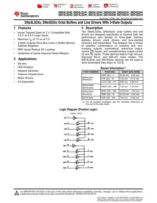
74LS245中文资料_数据手册_参数
- 格式:pdf
- 大小:2.41 MB
- 文档页数:31
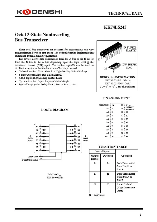
TECHNICAL DATAKK 74LS245Octal 3-State Noninverting Bus TransceiverThese octal bus transceiver are designed for asynchronous two-way communication between data buses. The control function implementation minimized external timing requirements.The device allows data transmission from the A bus to the B bus or from the B bus to the A bus depending upon the logic level at the directional control (DIR) input. The enable input(E) can be used to disable the device so that the buses are effectively isolated.• Bidirectional Bus Transceiver in a High-Density 20-Pin Package • 3-state Outputs Dirve Bus Lines Directly • P-N-P Inputs D-C Loading on Bus Lines• Hysteresis at Bus Inputs Improve Noise Margins• Typical Propagation Delay Times; Port to Port ... 8 nsPIN ASSIGNMENTLOGIC DIAGRAMPIN 20=V CC PIN 10 = GNDFUNCTION TABLEControl InputsOutput EnableDirection OperationL L Data Transmittedfrom Bus B to Bus A L H Data Transmittedfrom Bus A to Bus B H X Buses Isolated(High Impedance State) X = don’t careMAXIMUM RATINGS*Symbol Parameter ValueUnit V CC Supply Voltage 7.0 VV IN Input Voltage 7.0 VV OUT Output Voltage 5.5 VTstg Storage Temperature Range -65 to +150 °C*Maximum Ratings are those values beyond which damage to the device may occur.Functional operation should be restricted to the Recommended Operating Conditions.RECOMMENDED OPERATING CONDITIONSSymbol Parameter MinMaxUnit V CC Supply Voltage 4.75 5.25 VV IH High Level Input Voltage 2.0 VV IL Low Level Input Voltage 0.8 VI OH High Level Output Current -15 mAI OL Low Level Output Current 24 mAT A Ambient Temperature Range 0 +70 °CDC ELECTRICAL CHARACTERISTICS over full operating conditionsGuaranteedLimit Symbol Parameter TestConditions MinMaxUnit V IK Input Clamp Voltage V CC = min, I IN = -18 mA -1.5 VV OH High Level Output Voltage V CC = min, I OH = -1.0 mA 2.7 VV CC = min, I OH = -3.0 mA 2.4V CC = min, I OH = -15 mA 2.0V OL Low Level Output Voltage V CC = min, I OL = 12 mA 0.4 VV CC = min, I OL = 24 mA 0.5V T+ - V T-Hysteresis V CC = min 0.2 VI OZH Output Off Current HIGH V CC = max, V OUT = 2.7 V 20 µAI OZL Output Off Current LOW V CC = max, V OUT = 0.4 V -0.2 mAI IH High Level Input Current V CC = max, V IN = 2.7 V 20 µAV CC = max, V IN = 5.5 V (A or B) 0.1mAV CC = max, V IN = 7.0 Vfor Pin1, Pin 190.1I IL Low Level Input Current V CC = max, V IN = 0.4 V -0.2 mAI O Output Short Circuit Current V CC = max, V O =0 V(Note 1)-40 -225 mAI CC Supply OutputsHigh V CC = max 70 mA Current Outputs Low Outputs open 90All outputs disable 95Note 1: Not more thanone output should be shorted at a time, and duration of the short-circuit should not exceed one second.AC ELECTRICAL CHARACTERISTICS (T A = 25°C, V CC = 5.0 V, t r = 15 ns,,t f = 6.0 ns)Symbol Parameter TestConditionMinMaxUnitt PLH Propagation Delay Time, Low-to-High Level Output (from A or B to Output) 12nst PHL Propagation Delay Time, High-to-Low Level Output (from A or B to Output) C L = 45 pF,R L = 667 Ω12nst PZH Output Enable Time to High Level (from OE to Output) 40nst PZL Output Enable Time to Low Level (from OE to Output) 40nst PHZ Output Disable Time from High Level(from OE to Output) C L = 5 pF 25nst PLZ Output Disable Time from Low Level (from OE to Output) R L = 667 Ω 25nst PZL - S1 closed, S2 openedt PZH- S1 opened, S2 closedt PLZ, t PHZ - S1 and S2 closedFigure 1. Switching Waveforms(See Figure 3) Figure 2. Switching Waveforms(See Figure 4)NOTES A.C L includes probe and jig capacitance.B. All diodes are 1N916 or 1N3064.NOTES A.C L includes probe and jig capacitance.B. All diodes are 1N916 or 1N3064.Figure 3. Test Circuit Figure 4. Test CircuitEXPANDED LOGIC DIAGRAM。
Hitachi Code JEDEC EIAJWeight (reference value)DP-20N —Conforms 1.26 gUnit: mm元器件交易网Cautions1.Hitachi neither warrants nor grants licenses of any rights of Hitachi’s or any third party’s patent,copyright, trademark, or other intellectual property rights for information contained in this document.Hitachi bears no responsibility for problems that may arise with third party’s rights, includingintellectual property rights, in connection with use of the information contained in this document.2.Products and product specifications may be subject to change without notice. Confirm that you have received the latest product standards or specifications before final design, purchase or use.3.Hitachi makes every attempt to ensure that its products are of high quality and reliability. However,contact Hitachi’s sales office before using the product in an application that demands especially high quality and reliability or where its failure or malfunction may directly threaten human life or cause risk of bodily injury, such as aerospace, aeronautics, nuclear power, combustion control, transportation,traffic, safety equipment or medical equipment for life support.4.Design your application so that the product is used within the ranges guaranteed by Hitachi particularly for maximum rating, operating supply voltage range, heat radiation characteristics, installationconditions and other characteristics. Hitachi bears no responsibility for failure or damage when used beyond the guaranteed ranges. Even within the guaranteed ranges, consider normally foreseeable failure rates or failure modes in semiconductor devices and employ systemic measures such as fail-safes, so that the equipment incorporating Hitachi product does not cause bodily injury, fire or other consequential damage due to operation of the Hitachi product.5.This product is not designed to be radiation resistant.6.No one is permitted to reproduce or duplicate, in any form, the whole or part of this document without written approval from Hitachi.7.Contact Hitachi’s sales office for any questions regarding this document or Hitachi semiconductor products.Hitachi, Ltd.Semiconductor & Integrated Circuits.Nippon Bldg., 2-6-2, Ohte-machi, Chiyoda-ku, Tokyo 100-0004, Japan Tel: Tokyo (03) 3270-2111 Fax: (03) 3270-5109Copyright ' Hitachi, Ltd., 1999. All rights reserved. Printed in Japan.Hitachi Asia Pte. Ltd.16 Collyer Quay #20-00Hitachi TowerSingapore 049318Tel: 535-2100Fax: 535-1533URLNorthAmerica : http:/Europe : /hel/ecg Asia (Singapore): .sg/grp3/sicd/index.htm Asia (Taiwan): /E/Product/SICD_Frame.htm Asia (HongKong): /eng/bo/grp3/index.htm Japan : http://www.hitachi.co.jp/Sicd/indx.htmHitachi Asia Ltd.Taipei Branch Office3F, Hung Kuo Building. No.167, Tun-Hwa North Road, Taipei (105)Tel: <886> (2) 2718-3666Fax: <886> (2) 2718-8180Hitachi Asia (Hong Kong) Ltd.Group III (Electronic Components)7/F., North Tower, World Finance Centre,Harbour City, Canton Road, Tsim Sha Tsui,Kowloon, Hong Kong Tel: <852> (2) 735 9218Fax: <852> (2) 730 0281 Telex: 40815 HITEC HXHitachi Europe Ltd.Electronic Components Group.Whitebrook ParkLower Cookham Road MaidenheadBerkshire SL6 8YA, United Kingdom Tel: <44> (1628) 585000Fax: <44> (1628) 778322Hitachi Europe GmbHElectronic components Group Dornacher Stra§e 3D-85622 Feldkirchen, Munich GermanyTel: <49> (89) 9 9180-0Fax: <49> (89) 9 29 30 00Hitachi Semiconductor (America) Inc.179 East Tasman Drive,San Jose,CA 95134 Tel: <1> (408) 433-1990Fax: <1>(408) 433-0223For further information write to:。
74ls245原理
74LS245是一种双向总线缓冲器,用于将一个电路中的双向数据总线
与另一个电路中的双向数据总线相连接。
它有两个8位数据输入/输出端口(Port A和Port B),并且可以通过一个控制管脚(有时称为“使能”管脚)来选择数据流的方向。
在74LS245中,控制管脚(通常称为“使能”管脚)是“OE”,意
为“输出使能”。
当OE管脚为高电平(通常为Vcc)时,数据可以从端口A到端口B传输,而当OE管脚为低电平(通常为地)时,数据
可以从端口B到端口A传输。
该芯片中还有三个重要的管脚:DIR,A和B。
DIR管脚的状态决定了数据流的方向,当DIR管脚为高电平时,数据从端口A到端口B传输,当DIR管脚为低电平时,数据从端口B到端口A传输。
在使用时,DIR管脚通常与控制器中的某个输出位相连,以实现数据的控制。
在使用74LS245时,需要注意以下几点:
1. 端口A和端口B的电压级别必须相同(通常为TTL电平或CMOS
电平)。
2. 当数据从一个电路传输到另一个电路时,要确保电路之间的电气特性匹配,以避免信号失真。
3. 在数据传输期间,DIR管脚和OE管脚必须设置为正确的状态以实现正确的数据流。
总之,74LS245是一个方便实用的双向总线缓冲器,可以确保数据流动的可靠性和正确性。
在实际应用中,75LS245可以用于传输数据,例如在电子设备和自动控制系统中用于数据输入和输出。
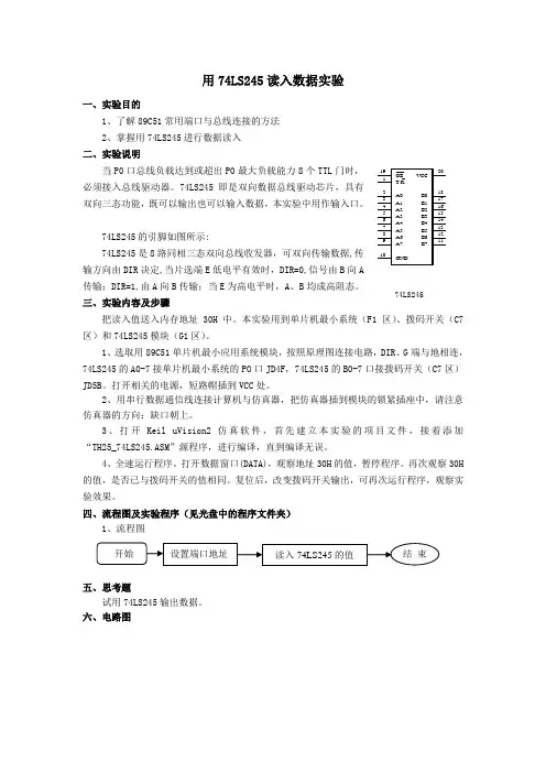
用74LS245读入数据实验一、实验目的1、了解89C51常用端口与总线连接的方法2、掌握用74LS245进行数据读入 二、实验说明当P0口总线负载达到或超出P0最大负载能力8个TTL 门时,必须接入总线驱动器。
74LS245即是双向数据总线驱动芯片,具有双向三态功能,既可以输出也可以输入数据,本实验中用作输入口。
74LS245的引脚如图所示:74LS245是8路同相三态双向总线收发器,可双向传输数据,传输方向由DIR 决定,当片选端E 低电平有效时,DIR=0,信号由B 向A 传输;DIR=1,由A 向B 传输;当E 为高电平时,A 、B 均成高阻态。
三、实验内容及步骤把读入值送入内存地址30H 中。
本实验用到单片机最小系统(F1区)、拨码开关(C7区)和74LS245模块(G1区)。
1、选取用89C51单片机最小应用系统模块,按照原理图连接电路,DIR 、G 端与地相连,74LS245的A0-7接单片机最小系统的PO 口JD4F ,74LS245的B0-7口接拨码开关(C7区)JD5B 。
打开相关的电源,短路帽插到VCC 处。
2、用串行数据通信线连接计算机与仿真器,把仿真器插到模块的锁紧插座中,请注意仿真器的方向:缺口朝上。
3、打开Keil uVision2仿真软件,首先建立本实验的项目文件,接着添加“TH25_74LS245.ASM ”源程序,进行编译,直到编译无误。
4、全速运行程序。
打开数据窗口(DATA),观察地址30H 的值,暂停程序。
再次观察30H 的值,是否已与拨码开关的值相同。
复位后,改变拨码开关输出,可再次运行程序,观察实验效果。
四、流程图及实验程序(见光盘中的程序文件夹)1、流程图 五、思考题试用74LS245输出数据。
六、电路图74LS245设置端口地址读入74LS245的值开始 结 束OE 19T/R 1A13B117A24B216A35B315A46B414A57B513A68B612A79B711A02B018VCC20GND10OE19T/R 1A13B117A24B216A35B315A46B414A57B513A68B612A79B711A02B018VCC20GND 10U1GSN74LS245N12345678JD2G B0-7VCCXTAL1A 12MHzC3A 33pFC2A 33pFP1.01P1.12P1.23P1.34P1.45P1.56P1.67P1.78RST 9P3.0/RXD 10P3.1/TXD 11P3.2/INT012P3.3/INT113P3.4/T014P3.5/T115P3.6/WR 16P3.7/RD 17XTAL218XTAL119VSS20P2.021P2.122P2.223P2.324P2.425P2.526P2.627P2.728PSEN 29ALE/PROG30EA31P0.032P0.133P0.234P0.335P0.436P0.537P0.638P0.739VCC 4089C51U1FVCC P3.0P3.1P1.0P1.1P1.2P1.3P1.4P1.5P1.6P1.7P0.0P0.1P0.2P0.3P0.4P0.5P0.6P0.7EAALE PSEN P2.7P2.6P2.5P2.4P2.3P2.2P2.1P2.0P3.2P3.3P3.4P3.5P3.6P3.7C3F 10uFVCCRESETR2F 100R1F 1K。
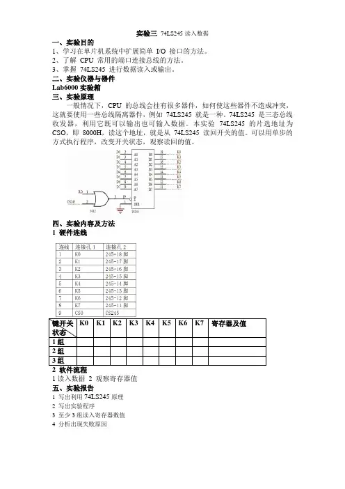
实验三74LS245读入数据
一、实验目的
1、学习在单片机系统中扩展简单I/O 接口的方法。
2、了解CPU 常用的端口连接总线的方法。
3、掌握74LS245 进行数据读入或输出。
二、实验仪器与器件
Lab6000实验箱
三、实验原理
一般情况下,CPU 的总线会挂有很多器件,如何使这些器件不造成冲突,这就要使用一些总线隔离器件,例如74LS245 就是一种。
74LS245 是三态总线收发器,利用它既可以输出也可输入数据。
本实验74LS245 的片选地址为CSO,即8000H,读这个地址,就是从74LS245 读回开关的值。
可以用单步的方式执行程序,改变开关状态,观察读回的值。
四、实验内容及方法
1 硬件连线
1读入数据2 观察寄存器值
五、实验报告
1 写出利用74LS245原理
2 写出实验程序
3 至少3组读入寄存器数值
4 分析出现失败原因。
单片机驱动芯片(74HC245)详细中文资料(74HC245是一款高速CMOS器件,74HC245引脚兼容低功耗肖特基TTL(LSTTL)系列) 74HC245译码器可接受3位二进制加权地址输入(A0, A1和A2),并当使能时,提供8个互斥的低有效输出(Y0至Y7)。
74HC245特有3个使能输入端:两个低有效(E1和E2)和一个高有效(E3)。
除非E1和E2置低且E3置高,否则74HC138将保持所有输出为高。
利用这种复合使能特性,仅需4片7 4HC245芯片和1个反相器,即可轻松实现并行扩展,组合成为一个1-32(5线到32线)译码器。
任选一个低有效使能输入端作为数据输入,而把其余的使能输入端作为选通端,则74HC245亦可充当一个8输出多路分配器,未使用的使能输入端必须保持绑定在各自合适的高有效或低有效状态。
74HC245与74HC238逻辑功能一致,只不过74HC138为反相输出。
一、功能CD74HC245 ,CD74HC238和CD74HCT245, CD74HCT238是高速硅栅CMOS解码器,适合内存地址解码或数据路由应用。
74HC245作用原理于高性能的存贮译码或要求传输延迟时间短的数据传输系统,在高性能存贮器系统中,用这种译码器可以提高译码系统的效率。
将快速赋能电路用于高速存贮器时,译码器的延迟时间和存贮器的赋能时间通常小于存贮器的典型存取时间,这就是说由肖特基钳位的系统译码器所引起的有效系统延迟可以忽略不计。
HC138 按照三位二进制输入码和赋能输入条件,从8 个输出端中译出一个低电平输出。
两个低电平有效的赋能输入端和一个高电平有效的赋能输入端减少了扩展所需要的外接门或倒相器,扩展成24 线译码器不需外接门;扩展成32 线译码器,只需要接一个外接倒相器。
在解调器应用中,赋能输入端可用作数据输入端。
特性复合使能输入,轻松实现扩展兼容JEDEC标准no.7A 存储器芯片译码选择的理想选择低有效互斥输出 ESD保护 HBM EIA/JESD22-A114-C超过2000 V MM EIA/JESD22-A115-A超过200 V 温度范围 -4 0~+85 ℃ -40~+125 ℃多路分配功能74HC245是一款高速CMOS器件,74HC245引脚兼容低功耗肖特基TTL(LSTTL)系列。
74HC245详细中文资料74HC245是一款高速CMOS器件,74HC2 45引脚兼容低功耗肖特基TTL(LSTTL)系列。
74HC245译码器可接受3位二进制加权地址输入(A0, A1和A2),并当使能时,提供8个互斥的低有效输出(Y0至Y7)。
74HC245特有3个使能输入端:两个低有效(E1和E2)和一个高有效(E3)。
除非E1和E2置低且E3置高,否则74HC138将保持所有输出为高。
利用这种复合使能特性,仅需4片74HC 245芯片和1个反相器,即可轻松实现并行扩展,组合成为一个1-32(5线到3 2线)译码器。
任选一个低有效使能输入端作为数据输入,而把其余的使能输入端作为选通端,则74HC245亦可充当一个8输出多路分配器,未使用的使能输入端必须保持绑定在各自合适的高有效或低有效状态。
74HC245与74HC 238逻辑功能一致,只不过74HC138为反相输出。
功能CD74HC245 ,CD74HC238和CD74HCT245,CD74HCT238是高速硅栅CMOS解码器,适合内存地址解码或数据路由应用。
74HC245作用原理于高性能的存贮译码或要求传输延迟时间短的数据传输系统,在高性能存贮器系统中,用这种译码器可以提高译码系统的效率。
将快速赋能电路用于高速存贮器时,译码器的延迟时间和存贮器的赋能时间通常小于存贮器的典型存取时间,这就是说由肖特基钳位的系统译码器所引起的有效系统延迟可以忽略不计。
HC138 按照三位二进制输入码和赋能输入条件,从8 个输出端中译出一个低电平输出。
两个低电平有效的赋能输入端和一个高电平有效的赋能输入端减少了扩展所需要的外接门或倒相器,扩展成24 线译码器不需外接门;扩展成32 线译码器,只需要接一个外接倒相器。
在解调器应用中,赋能输入端可用作数据输入端。
特性复合使能输入,轻松实现扩展兼容JEDEC标准no.7A 存储器芯片译码选择的理想选择低有效互斥输出ESD保护HBM EIA/JESD22-A114-C超过20 00 V MM EIA/JESD22-A115-A超过200 V 温度范围-40~+85 ℃-40~+12 5 ℃多路分配功能 74HC245是一款高速CMOS器件,74HC245引脚兼容低功耗肖特基TTL(LSTTL)系列。
74ls系列中文资料功能介绍(注:红色为实验室已有器件)型号功能----------------------------------------------------74ls00 2输入四与非门74ls01 2输入四与非门(oc)74ls02 2输入四或非门74ls03 2输入四与非门(oc)74ls04 六倒相器74ls05 六倒相器(oc)74ls06 六高压输出反相缓冲器/驱动器(oc,30v) 74ls07 六高压输出缓冲器/驱动器(oc,30v)74ls08 2输入四与门74ls09 2输入四与门(oc)74ls10 3输入三与非门74ls11 3输入三与门74ls12 3输入三与非门(oc)74ls13 4输入双与非门(斯密特触发)74ls14 六倒相器(斯密特触发)74ls15 3输入三与门(oc)74ls16 六高压输出反相缓冲器/驱动器(oc,15v) 74ls17 六高压输出缓冲器/驱动器(oc,15v)74ls18 4输入双与非门(斯密特触发)74ls19 六倒相器(斯密特触发)74ls20 4输入双与非门74ls21 4输入双与门74ls22 4输入双与非门(oc)74ls23 双可扩展的输入或非门74ls24 2输入四与非门(斯密特触发)74ls25 4输入双或非门(有选通)74ls26 2输入四高电平接口与非缓冲器(oc,15v) 74ls27 3输入三或非门74ls28 2输入四或非缓冲器74ls30 8输入与非门74ls31 延迟电路74ls32 2输入四或门74ls33 2输入四或非缓冲器(集电极开路输出)74ls34 六缓冲器74ls35 六缓冲器(oc)74ls36 2输入四或非门(有选通)74ls37 2输入四与非缓冲器74ls38 2输入四或非缓冲器(集电极开路输出)74ls39 2输入四或非缓冲器(集电极开路输出)74ls40 4输入双与非缓冲器74ls41 bcd-十进制计数器74ls42 4线-10线译码器(bcd输入)74ls43 4线-10线译码器(余3码输入)74ls44 4线-10线译码器(余3葛莱码输入)74ls45 bcd-十进制译码器/驱动器74ls46 bcd-七段译码器/驱动器74ls47 bcd-七段译码器/驱动器74ls48 bcd-七段译码器/驱动器74ls49 bcd-七段译码器/驱动器(oc)74ls50 双二路2-2输入与或非门(一门可扩展)74ls51 双二路2-2输入与或非门74ls51 二路3-3输入,二路2-2输入与或非门74ls52 四路2-3-2-2输入与或门(可扩展)74ls53 四路2-2-2-2输入与或非门(可扩展)74ls53 四路2-2-3-2输入与或非门(可扩展)74ls54 四路2-2-2-2输入与或非门74ls54 四路2-3-3-2输入与或非门74ls54 四路2-2-3-2输入与或非门74ls55 二路4-4输入与或非门(可扩展)74ls60 双四输入与扩展74ls61 三3输入与扩展74ls62 四路2-3-3-2输入与或扩展器74ls63 六电流读出接口门74ls64 四路4-2-3-2输入与或非门74ls65 四路4-2-3-2输入与或非门(oc)74ls70 与门输入上升沿jk触发器74ls71 与输入r-s主从触发器74ls72 与门输入主从jk触发器74ls73 双j-k触发器(带清除端)74ls74 正沿触发双d型触发器(带预置端和清除端)74ls75 4位双稳锁存器74ls76 双j-k触发器(带预置端和清除端)74ls77 4位双稳态锁存器74ls78 双j-k触发器(带预置端,公共清除端和公共时钟端) 74ls80 门控全加器74ls81 16位随机存取存储器74ls82 2位二进制全加器(快速进位)74ls83 4位二进制全加器(快速进位)74ls84 16位随机存取存储器74ls85 4位数字比较器74ls86 2输入四异或门74ls87 四位二进制原码/反码/oi单元74ls89 64位读/写存储器74ls90 十进制计数器74ls91 八位移位寄存器74ls92 12分频计数器(2分频和6分频)74ls93 4位二进制计数器74ls94 4位移位寄存器(异步)74ls95 4位移位寄存器(并行io)74ls96 5位移位寄存器74ls97 六位同步二进制比率乘法器74ls100 八位双稳锁存器74ls103 负沿触发双j-k主从触发器(带清除端)74ls106 负沿触发双j-k主从触发器(带预置,清除,时钟) 74ls107 双j-k主从触发器(带清除端)74ls108 双j-k主从触发器(带预置,清除,时钟)74ls109 双j-k触发器(带置位,清除,正触发)74ls110 与门输入j-k主从触发器(带锁定)74ls111 双j-k主从触发器(带数据锁定)74ls112 负沿触发双j-k触发器(带预置端和清除端)74ls113 负沿触发双j-k触发器(带预置端)74ls114 双j-k触发器(带预置端,共清除端和时钟端)74ls116 双四位锁存器74ls120 双脉冲同步器/驱动器74ls121 单稳态触发器(施密特触发)74ls122 可再触发单稳态多谐振荡器(带清除端)74ls123 可再触发双单稳多谐振荡器74ls125 四总线缓冲门(三态输出)74ls126 四总线缓冲门(三态输出)74ls128 2输入四或非线驱动器74ls131 3-8译码器74ls132 2输入四与非门(斯密特触发)74ls133 13输入端与非门74ls134 12输入端与门(三态输出)74ls135 四异或/异或非门74ls136 2输入四异或门(oc)74ls137 八选1锁存译码器/多路转换器74ls138 3-8线译码器/多路转换器74ls139 双2-4线译码器/多路转换器74ls140 双4输入与非线驱动器74ls141 bcd-十进制译码器/驱动器74ls142 计数器/锁存器/译码器/驱动器74ls145 4-10译码器/驱动器74ls147 10线-4线优先编码器74ls148 8线-3线八进制优先编码器74ls150 16选1数据选择器(反补输出)74ls151 8选1数据选择器(互补输出)74ls152 8选1数据选择器多路开关74ls153 双4选1数据选择器/多路选择器74ls154 4线-16线译码器74ls155 双2-4译码器/分配器(图腾柱输出)74ls156 双2-4译码器/分配器(集电极开路输出) 74ls157 四2选1数据选择器/多路选择器74ls158 四2选1数据选择器(反相输出)74ls160 可预置bcd计数器(异步清除)74ls161 可预置四位二进制计数器(并清除异步) 74ls162 可预置bcd计数器(异步清除)74ls163 可预置四位二进制计数器(并清除异步) 74ls164 8位并行输出串行移位寄存器74ls165 并行输入8位移位寄存器(补码输出) 74ls166 8位移位寄存器74ls167 同步十进制比率乘法器74ls168 4位加/减同步计数器(十进制)74ls169 同步二进制可逆计数器74ls170 4*4寄存器堆74ls171 四d触发器(带清除端)74ls172 16位寄存器堆74ls173 4位d型寄存器(带清除端)74ls174 六d触发器74ls175 四d触发器74ls176 十进制可预置计数器74ls177 2-8-16进制可预置计数器74ls178 四位通用移位寄存器74ls179 四位通用移位寄存器74ls180 九位奇偶产生/校验器74ls181 算术逻辑单元/功能发生器74ls182 先行进位发生器74ls183 双保留进位全加器74ls184 bcd-二进制转换器74ls185 二进制-bcd转换器74ls190 同步可逆计数器(bcd,二进制)74ls191 同步可逆计数器(bcd,二进制)74ls192 同步可逆计数器(bcd,二进制)74ls193 同步可逆计数器(bcd,二进制)74ls194 四位双向通用移位寄存器74ls195 四位通用移位寄存器74ls196 可预置计数器/锁存器74ls197 可预置计数器/锁存器(二进制)74ls198 八位双向移位寄存器74ls199 八位移位寄存器74ls210 2-5-10进制计数器74ls213 2-n-10可变进制计数器74ls221 双单稳触发器74ls230 八3态总线驱动器74ls231 八3态总线反向驱动器74ls240 八缓冲器/线驱动器/线接收器(反码三态输出) 74ls241 八缓冲器/线驱动器/线接收器(原码三态输出) 74ls242 八缓冲器/线驱动器/线接收器74ls243 4同相三态总线收发器74ls244 八缓冲器/线驱动器/线接收器74ls245 八双向总线收发器74ls246 4线-七段译码/驱动器(30v)74ls247 4线-七段译码/驱动器(15v)74ls248 4线-七段译码/驱动器74ls249 4线-七段译码/驱动器74ls251 8选1数据选择器(三态输出)74ls253 双四选1数据选择器(三态输出)74ls256 双四位可寻址锁存器74ls257 四2选1数据选择器(三态输出)74ls258 四2选1数据选择器(反码三态输出)74ls259 8为可寻址锁存器74ls260 双5输入或非门74ls261 4*2并行二进制乘法器74ls265 四互补输出元件74ls266 2输入四异或非门(oc)74ls270 2048位rom (512位四字节,oc)74ls271 2048位rom (256位八字节,oc)74ls273 八d触发器74ls274 4*4并行二进制乘法器74ls275 七位片式华莱士树乘法器74ls276 四jk触发器74ls278 四位可级联优先寄存器74ls279 四s-r锁存器74ls280 9位奇数/偶数奇偶发生器/较验器74ls28174ls283 4位二进制全加器74ls290 十进制计数器74ls291 32位可编程模74ls293 4位二进制计数器74ls294 16位可编程模74ls295 四位双向通用移位寄存器74ls298 四-2输入多路转换器(带选通)74ls299 八位通用移位寄存器(三态输出)74ls348 8-3线优先编码器(三态输出)74ls352 双四选1数据选择器/多路转换器74ls353 双4-1线数据选择器(三态输出)74ls354 8输入端多路转换器/数据选择器/寄存器,三态补码输出74ls355 8输入端多路转换器/数据选择器/寄存器,三态补码输出74ls356 8输入端多路转换器/数据选择器/寄存器,三态补码输出74ls357 8输入端多路转换器/数据选择器/寄存器,三态补码输出74ls365 6总线驱动器74ls366 六反向三态缓冲器/线驱动器74ls367 六同向三态缓冲器/线驱动器74ls368 六反向三态缓冲器/线驱动器74ls373 八d锁存器74ls374 八d触发器(三态同相)74ls375 4位双稳态锁存器74ls377 带使能的八d触发器74ls378 六d触发器74ls379 四d触发器74ls381 算术逻辑单元/函数发生器74ls382 算术逻辑单元/函数发生器74ls384 8位*1位补码乘法器74ls385 四串行加法器/乘法器74ls386 2输入四异或门74ls390 双十进制计数器74ls391 双四位二进制计数器74ls395 4位通用移位寄存器74ls396 八位存储寄存器74ls398 四2输入端多路开关(双路输出)74ls399 四-2输入多路转换器(带选通)74ls422 单稳态触发器74ls423 双单稳态触发器74ls440 四3方向总线收发器,集电极开路74ls441 四3方向总线收发器,集电极开路74ls442 四3方向总线收发器,三态输出74ls443 四3方向总线收发器,三态输出74ls444 四3方向总线收发器,三态输出74ls445 bcd-十进制译码器/驱动器,三态输出74ls446 有方向控制的双总线收发器74ls448 四3方向总线收发器,三态输出74ls449 有方向控制的双总线收发器74ls465 八三态线缓冲器74ls466 八三态线反向缓冲器74ls467 八三态线缓冲器74ls468 八三态线反向缓冲器74ls490 双十进制计数器74ls540 八位三态总线缓冲器(反向)74ls541 八位三态总线缓冲器74ls589 有输入锁存的并入串出移位寄存器74ls590 带输出寄存器的8位二进制计数器74ls591 带输出寄存器的8位二进制计数器74ls592 带输出寄存器的8位二进制计数器74ls593 带输出寄存器的8位二进制计数器74ls594 带输出锁存的8位串入并出移位寄存器74ls595 8位输出锁存移位寄存器74ls596 带输出锁存的8位串入并出移位寄存器74ls597 8位输出锁存移位寄存器74ls598 带输入锁存的并入串出移位寄存器74ls599 带输出锁存的8位串入并出移位寄存器74ls604 双8位锁存器74ls605 双8位锁存器74ls606 双8位锁存器74ls607 双8位锁存器74ls620 8位三态总线发送接收器(反相)74ls621 8位总线收发器74ls622 8位总线收发器74ls623 8位总线收发器74ls640 反相总线收发器(三态输出)74ls641 同相8总线收发器,集电极开路74ls642 同相8总线收发器,集电极开路74ls643 8位三态总线发送接收器74ls644 真值反相8总线收发器,集电极开路74ls645 三态同相8总线收发器74ls646 八位总线收发器,寄存器74ls647 八位总线收发器,寄存器74ls648 八位总线收发器,寄存器74ls649 八位总线收发器,寄存器74ls651 三态反相8总线收发器74ls652 三态反相8总线收发器74ls653 反相8总线收发器,集电极开路74ls654 同相8总线收发器,集电极开路74ls668 4位同步加/减十进制计数器74ls669 带先行进位的4位同步二进制可逆计数器74ls670 4*4寄存器堆(三态)74ls671 带输出寄存的四位并入并出移位寄存器74ls672 带输出寄存的四位并入并出移位寄存器74ls673 16位并行输出存储器,16位串入串出移位寄存器74ls674 16位并行输入串行输出移位寄存器74ls681 4位并行二进制累加器74ls682 8位数值比较器(图腾柱输出)74ls683 8位数值比较器(集电极开路)74ls684 8位数值比较器(图腾柱输出)74ls685 8位数值比较器(集电极开路)74ls686 8位数值比较器(图腾柱输出)74ls687 8位数值比较器(集电极开路)74ls688 8位数字比较器(oc输出)74ls689 8位数字比较器74ls690 同步十进制计数器/寄存器(带数选,三态输出,直接清除)74ls691 计数器/寄存器(带多转换,三态输出)74ls692 同步十进制计数器(带预置输入,同步清除)74ls693 计数器/寄存器(带多转换,三态输出)74ls696 同步加/减十进制计数器/寄存器(带数选,三态输出,直接清除) 74ls697 计数器/寄存器(带多转换,三态输出)74ls698 计数器/寄存器(带多转换,三态输出)74ls699 计数器/寄存器(带多转换,三态输出)74ls716 可编程模n十进制计数器74ls718 可编程模n十进制计数器。
LOW POWER SCHOTTKYDevice Package Shipping SN74LS245N 16 Pin DIP 1440 Units/Box SN74LS245DW16 PinSOIC DW SUFFIX CASE 751D2500/T ape & ReelPLASTIC N SUFFIX CASE 738201201ON Semiconductor and are trademarks of Semiconductor Components Industries, LLC (SCILLC). SCILLC reserves the right to make changes without further notice to any products herein. SCILLC makes no warranty, representation or guarantee regarding the suitability of its products for any particular purpose, nor does SCILLC assume any liability arising out of the application or use of any product or circuit, and specifically disclaims any and all liability, including without limitation special, consequential or incidental damages. “Typical” parameters which may be provided in SCILLC data sheets and/or specifications can and do vary in different applications and actual performance may vary over time. All operating parameters, including “Typicals” must be validated for each customer application by customer’s technical experts. SCILLC does not convey any license under its patent rights nor the rights of others.SCILLC products are not designed, intended, or authorized for use as components in systems intended for surgical implant into the body, or other applications intended to support or sustain life, or for any other application in which the failure of the SCILLC product could create a situation where personal injury or death may occur. Should Buyer purchase or use SCILLC products for any such unintended or unauthorized application, Buyer shall indemnify and hold SCILLC and its officers, employees, subsidiaries, affiliates, and distributors harmless against all claims, costs, damages, and expenses, and reasonable attorney fees arising out of, directly or indirectly, any claim of personal injury or death associated with such unintended or unauthorized use, even if such claim alleges that SCILLC was negligent regarding the design or manufacture of the part. SCILLC is an Equal Opportunity/Affirmative Action Employer. PUBLICATION ORDERING INFORMATIONASIA/PACIFIC: LDC for ON Semiconductor – Asia SupportPhone:303–675–2121 (Tue–Fri 9:00am to 1:00pm, Hong Kong Time)Toll Free from Hong Kong 800–4422–3781Email: ONlit–asia@JAPAN: ON Semiconductor, Japan Customer Focus Center4–32–1 Nishi–Gotanda, Shinagawa–ku, Tokyo, Japan 141–8549Phone: 81–3–5487–8345Email: r14153@Fax Response Line:303–675–2167。
带使能功能的八位双向总线驱动器74HC245 中文资料
这种八位总线收发器是为数据总线间进行异步两路通讯而设计的。
采用控制功能可以尽量减少外部定时电路的要求。
这种电路可以将数据从A 总线传送到B 总线,也可将数据从B 总线传送到 A 总线,具体传送方向要看方向控制(DIR)输入的逻辑电平而定。
可以用使能输入来禁止这种电路,使总线之间能有效地隔离。
74HC245真值表:
TRUTH TABLE真值表
H=高电平 L=低电平×=不定
74HC245电气参数:
Note 1: Maximum Ratings are those values beyond which damage to the
device may occur.
Note 2: Unless otherwise specified all voltages are referenced to ground. Note 3: Power Dissipation temperature derating —plastic “N” package: 12 mW/℃ from 65℃ to 85℃.
DC SPECIFICATIONS直流电气规格
AC Electrical C haracteristics VCC=5V, TA=25℃, tr= tf =6ns交流电气特性
AC Electrical Characteristics VCC=2.0V to 6.0V, CL=50 pF, t r= tf =6ns 交流电气特性。
74ls245
74LS245是我们常用的芯片,用来驱动led或者其他的设备,它是8路同相三态双向总线收发器,可双向传输数据。
74LS245还具有双向三态功能,既可以输出,也可以输入数据。
当8051单片机的P0口总线负载达到或超过P0最大负载能力时,必须接入74LS245等总线驱动器。
当片选端/CE低电平有效时,DIR=“0”,信号由 B 向 A 传输;(接收)DIR=“1”,信号由 A 向 B 传输;(发送)当CE为高电平时,A、B 均为高阻态。
由于P2口始终输出地址的高8位,接口时74LS245的三态控制端1G
和2G接地,P2口与驱动器输入线对应相连。
P0口与74LS245输入端相连,E 端接地,保证数据线畅通。
8051的/RD和/PSEN相与后接DIR,使得RD且PSEN有效时,74LS245输入(P0.1←D1),其它时间处于输出(P0.1→D1)。