tlc5620中文资料
- 格式:doc
- 大小:52.50 KB
- 文档页数:7
tlc5620中文资料
2010-01-13 11:00
TLC5620C, TLC5620I
QUADRUPLE 8-BIT DIGITAL-TO-ANALOG CONVERTERS
Four 8-Bit Voltage Output DACs
4通道8位电压输出D/A转换器。
5-V Single-Supply Operation
5V单电源
Serial Interface
串行接口
High-Impedance Reference Inputs
高阻抗的基准输入
Programmable 1 or 2 Times Output Range
可编程实现1至2倍的输出范围
Simultaneous Update Facility
设备可同时进行更新
Internal Power-On Reset
内置上电复位
Low-Power Consumption
低功耗
Half-Buffered Output
半缓冲输出
Applications
应用 Programmable Voltage Sources
可编程电源
Digitally Controlled Amplifiers/Attenuators
可数字控制的放大器和衰减器
Mobile Communications
移动通信
Automatic Test Equipment
自动测试设备
Process Monitoring and Control
过程监控
Signal Synthesis
信号合成
Description
描述
The TLC5620C and TLC5620I are quadruple 8-bit voltage output
digital-to-analog converters (DACs) with buffered reference inputs (high
impedance). The DACs produce an output voltage that ranges between either
one or two times the reference voltages and GND, and the DACs are
monotonic. The device is simple to use, running from a single supply of
5 V. A power-on reset function is incorporated to ensure repeatable
start-up conditions.
TLC5620C和TLC5620I是带有高阻抗缓冲输入的4通道8位电源输出数模转换器集合。这些转换器可以产生单调的、1至两倍于基准电压和接地电压差值的输出。通常情况下TLC5620的供电电压为一个5V电源。器件内集成上电复位功能,确保启动时的环境是可重复的。
Digital control of the TLC5620C and TLC5620I are over a simple three-wire
serial bus that is CMOS compatible and easily interfaced to all popular
microprocessor and microcontroller devices. The 11-bit command word
comprises eight bits of data, two DAC-select bits, and a range bit, the
latter allowing selection between the times 1 or times 2 output range. The DAC registers are double buffered, allowing a complete set of new
values to be written to the device, then all DAC outputs are updated
simultaneously through control of LDAC. The digital inputs feature
Schmitt triggers for high noise immunity.
对TLC5620C和TLC5620I的数字控制是通过一根简单的3路串行总线实现的。该总线兼容CMOS,并易于向所有的微处理器和微控制器设备提供接口。11位的命令字包括8位数据位,2位DAC选择位和1位范围位,后者用来选择输出范围是1倍还是2倍。DAC寄存器采用双缓存,允许一整套新值被写入设备中。通过LDAC实现DAC输出值的同时更新。数字量的输入采用史密斯触发器,从而避免了高噪声。
The 14-terminal small-outline (D) package allows digital control of
analog functions in space-critical applications. The TLC5620C is
characterized for operation from 0°C to 70°C. The TLC5620I is
characterized for operation from –40°C to 85°C. The TLC5620C and
TLC5620I do not require external trimming.
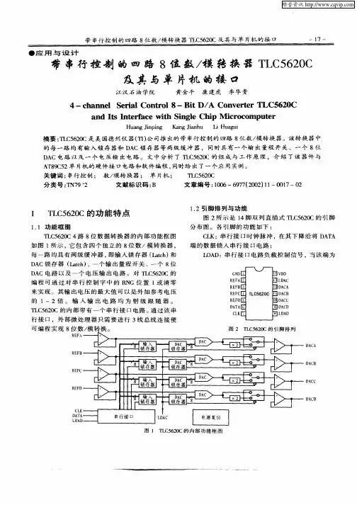
引脚 输入/输出 描述
名称 序号
CLK 7 I 串行接口时钟。引脚出现下降沿时将输入的数字量转发到串行接口寄存器里
DACA 12 O DAC A模拟信号输出
DACB 11 O DAC B模拟信号输出
DACC 10 O DAC C模拟信号输出
DACD 9 O DAC D模拟信号输出
DATA 6 I 存放数字量的串行接口
GND 1 I 地回路及参考终端
LDAC 13 I 加载DAC。当引脚出现高电平时,即使有数字量被读入串行口也不会对DAC
的输出进行更新。只有当引脚从高电平变为低电平时,DAC输出才更新。
LOAD 8 I 串口加载控制。当LDAC是低电平,并且LOAD引脚出现下降沿时数字量被保
存到锁存器,随后输出端产生模拟电压。
REFA 2 I 输入到DAC A的参考电压。这个电压定义了输出模拟量的范围。
REFB 3 I 输入到DAC B的参考电压。这个电压定义了输出模拟量的范围。
REFC 4 I 输入到DAC C的参考电压。这个电压定义了输出模拟量的范围。
REFD 5 I 输入到DAC D的参考电压。这个电压定义了输出模拟量的范围。
VDD 14 I 正极电源
周立功《ARM嵌入式系统实验教程》(三)中的代码:
/****************************************************************************
* 文 件 名:main.c
* 功 能:该实验程序使用TLC5620中A、B、C、D四个通道分别输出周期、幅度相等的
* 锯齿波,频率为6.35Hz。
* 说 明:跳线器JP1、JP2短接。
****************************************************************************/
#include "config.h"
#define
DAC_RNG 1
// 幅值选择
/* TLC5620由P0口控制,控制I/O定义如下 */
#define CLK1 (1<<21)
#define DAT1 (1<<22)
#define LOAD (1<<23)
#define LDAC (1<<24)
#define DAC5620CON (CLK1 | DAT1 | LOAD | LDAC)
/* I/O输出操作函数 */
#define CCLK1() IO1SET = CLK1
#define SCLK1() IO1CLR = CLK1
#define CDAT1() IO1SET = DAT1
#define SDAT1() IO1CLR = DAT1
#define CLOAD() IO1SET = LOAD
#define SLOAD() IO1CLR = LOAD
#define CLDAC() IO1SET = LDAC
#define SLDAC() IO1CLR = LDAC
void DAC5620_Data(uint8 no, uint8 dat);
void PIN_Init(void); void Delay(void);
int main(void)
{ uint8 i;
PIN_Init();
// 初始化CPU的IO口
while(1)
// 发生锯齿波
{
DAC5620_Data(1, i);
DAC5620_Data(2, i);
DAC5620_Data(3, i);
DAC5620_Data(4, i);
i++;
}
return(0);
}
/****************************************************************************
* 名 称:IRQ_Eint3()
* 功 能:外部中断EINT3服务函数,取反B1控制口。
* 入口参数:无
* 出口参数:无
****************************************************************************/
void
PIN_Init(void)
// CPU的IO口初始化函数
{
PINSEL0 = 0x00000000;
PINSEL1 = 0x00000000;
IO1DIR = DAC5620CON;
CCLK1();
// CLK1 = 0
CDAT1();
// DAT1 = 0
SLOAD();