AltiumDesigner自学电子笔记
- 格式:doc
- 大小:4.18 MB
- 文档页数:51
1.VU 快速切换单位,直接按Q也可以切换。
当调出一个对话框时,要更改单位可以点击左上角的图标或者按CTRL+Q也可以快速单位切换。
2.G 可以将栅格在1 5 10mil三个级别间切换3.原理图放置引脚时可以设置自增加或者自减少,在tools->preferences中,找到schematic 的general中的auto-increment during placement中设置,可以数字增减和字母增减。
4.创建snippet可以减少工作量,将一个电路模块作为一个整体进行设计。
5.多层设计是有三种网络范围,平行设计和分层设计均可。
可在project options->options->net identifier scope种进行设置。
6.PCB绘制时可以通过向导生成板子,同时确定板子的大小等信息。
7.F2 在PCB模式下是BOARDINSIGHT 的快捷键可以选择不同的模式来查看板子。
SHITF + H显示左上角的信息提示8.pcb状态下,打开PCB面板,第一项设置NETS,下面选择Mask,则选中的网络会以高亮显示,并且可以设置选中状态,这个比较方便。
9.View->Flip Board 板子翻转,从背面查看。
10.tools->cross probe 可以找出原理图和PCB之间的对应关系,在两者之间快速切换。
11.tools->convert->explodecomponent to free primitives 将一个完整的封装器件打散,可以独立的编辑其引脚,焊盘,外形等。
这个convert菜单很多,有空研究。
12.在TP选项中的true type fonts 中,使能这个字体的话就可以在PCB中放置中文。
13.工具条右边的Filter也非常强大,自己好好摸索下。
14.快速切换信号层,按小键盘的*号键,所有层切换+ 或者-方向不同,自己体会。
一PCB设计流程图二一些使用技巧(1)修改多个元件参数可以先选中一个元件,再右键选择Find Similar Objects,在弹出的对话框中,选择屏蔽选项,比如在Symbol Reference中将any改为some。
然后确定,就出现SCH Inspector。
然后就可以在Inspector中修改多个器件的参数或者封装。
(2)快速更改封装可以在Tools菜单栏中选择Footprint Manager,修改封装时候只要在封装上右键选择Set As Current, 更改完了以后点击Accept Changes。
另外,还可以右键选择Validate Footprint Paths来验证封装是否可用。
选择Accept后再点击Validate Changes可以查看更改是否可行,然后点击Execute Changes来执行更改。
另外,可以在Parameter Manager中修改参数。
(3)如何将别人的一个工程中用到的元件生成原理图库Tools中的Reset Schematic Designators来将器件复位成?状态。
或者在Annotate Schematics中选择Reset。
在Design中,选择Make Schematic Library来生成原理图库。
可以在Design中,选择Template,在其中选择模版来编辑原理图的一些信息,比如图名。
(4)如何将几个元件合并方法1,选中后右键,选择Unions方法2,选中元件,点击Tools菜单,然后选择Convert,再选择Creat Union(5)如何将某一部分经常使用的电路保存供以后使用选中后右键,选择Snippet,然后可以创建自己的Snipp et文件夹。
使用的时候,在右下角System菜单选择Snippet即可弹出窗口(6)如何得到元件报表选择Report,然后选择Bill of materials(7)自上而下的设计先使用Place Sheet Symbol再用Place Sheet Entry(注意按Tab键设置输入输出等属性),另外电源具有全局属性,不需另外设计。

一、汉化步骤:
打开ad 6.9软件,选择DXP|proferences命令,将弹出的prooferences对话框,
将其中localization分组框中的use localized resources 复选框选中,点击
应用,退出软件重启后将被汉化。
二、放置元件技巧:
在搜索元件时,通配符“*”是十分重要的,灵活运用通配符可以迅速精确
地找到所需的元件。
在放置元件状态下,按空格键可以逆时针旋转元件,按shift+空格键可以
顺时针旋转元件,按X键可以左右翻转元件,按Y键可以上下翻转元件。
元件放置快捷键:P 比如放置线: p w
在放置线时提供了4中模式 :1)90度放置 2)45度 3)任意角度 4)自动放置 通过shift+空格键来切换
总线的放置与线基本相同,不同点:总线不能直接与引脚相连,必须通过总线
进口连接。
网络标号注意事项:不能把网络标号放在总线上 ,否则编译的时候会出错。
节点的放置: 对于丁字交叉系统会自动放置节点,如果是十字交叉则必须手工
放置节点 p j
放置【没有ERC(No ERC)】标志的目的是在ERC(电气规则)检查时跳过对放置
此节点的检查,避免在编译中出错。
例如系统默认元件引脚必须连接,但是某些
芯片的引脚可以不连接,如果不放置此标志系统编译时就会认为此脚出错,导致
编译失败。
注意:在原理图中导线和直线具有不同的意义,直线不具有电气属性,在系统
编译时不处理直线。

Altium designer原理图的设计2、3、屏障:compile mask(编译时被屏障的不显示信息)。
4、消除编译警告:place→divectives→NO ERC。
5、6、放置总线BUS:总线名[0:n],然后place Bus Entry, 放置网络代码:place→ Net Label。
例如: 总线格式:databus[0:9],在Bus Entry命名:databus0、databus2… databus9,另一端命名databus0、databus2…databus9则建立了一一对应的关系,及databus0对应databus0。
7、查找替换:Edit→Find and Replace Text 说明:替换名字而已。
8、9、10、SCH→SCH Inspector 显示信息和修改被选对象参数等。
11、12、原理图设计完成后生成报表:reports→bill of materials,按键Export则导出元件清单/也可以使用模版“Template”点击浏览“*…+”选择模版再导出元件清单。
原理图分等级式的设计1、由顶层到底层设计:先设计顶层建立连接关系,然后创建子图再进行部分原理的设计并保存。
Place→sheet symbol命名编辑后,放置端口:place→add sheet entry,在弹出的窗口设置properties下的name 格式:名[0..n]。
多根线端口用总线连接。
子图的生成:左键单击选中sheet symbol,右击在弹出的菜单中选择create symbol actions→create sheet from sheet symbol。
设计完成之后进行检测确定是否匹配:Design→synchronize sheet entries and ports,如不匹配则修改之。
2、由底层到顶层设计:先设计原理图再由原理图创建sheet symbol再建立连接关系子图设计完成→创建原理图(可命名为top)→在工作区间单击右键→sheet actions→create sheet symbol from sheet or HDL→在弹出的对话框中选择子图→确定。
Altiumdesignersummer08学习笔记本人来自于重庆邮电大学,花了一个月时间学习altiumdesigner,学习过程中做了些简单的操作笔记,笔记是根据郭天祥的讲课视频来记录的,希望能对大家有所帮助,如果有什么想和我交流,可以加我的QQ:375240364开始启动ALTIUM DESIGNER时,其实运行的是DXP。
EXE文件,pcb画图要测量元件的大小,按ctrl+g能设置两个点之间的距离,选中弹出来工俱第二个图标为焊盘,画点,尺子测量ctrl+m,SHIFT+M是打开或取消放大镜功能,放大某一个部分画电路元件:1。
place下选要画的元件的形状,2,tool下选择PIN要添加的引脚,按TAB键可以修改引脚属性,(内部标号和外部号),确定后可按空格键翻转两个标号,3,按住CTRL键滚轮可以放大或缩小,4,在做原理图时,每个字母后面加上"\",就会显示上划线,这一条只适用于在画原理图库时,在原理图中添加元器件时修改其名字时是行不通的。
5,元件之间能自动连接,不过连接时的线是很短的,如何加长?按左键选中元件,然后按住CTRL键拖动元件。
6,添加封装,双击元件,再点击右下脚ADD,选择FOOTPRINT,7,2.54mm,在PCB中非常重要,即是100mil,单片机中大部分都是这样的距离,8。
画PCB封装图,元件都齐,再测量9,画PCB时设置两个引脚之间的距离:点工具栏#字网状图形,选set snap..默认的是mil单位,按Q后会转换成MM为单位,点焊盘画圆圈,按TAB键打开属性,designator中要填写与对应引脚相同的序号,画完后最好加一个框架。
加框要加在TOP OVERLAY层,用LINE画线工具画线,可以通过设置间距,使方框细一些,10.VSS是代表要接地的意思11,画好原理图后,选PROJECT下的compile编译,然后点designer下生成PCB图,然后点工具栏上的放大镜会弹出PCB图来,designer下bord shap下选redfine board shap来确定黑色格子的大小,最好和PCB图宽度相当12,画好一个PCB封装库时要设置一个参考点,以免到时移动时找不到元件,在封装库文件下点EDIT找到set reference,如果是在生成PCB之后才设置参考点,那么这时要重新导入封装,或是把库升级(找到工程里文件点右键升级),如果还是找不着位置,可以重置其坐标,找一个与它相差不远的元件的坐标,以它为参考设置。
郭天祥Altium Designer6.9 - 学习笔记听课笔记1. 查看某一元器件时按住Ctrl 滑动滑轮――就可以放大或缩小了,另一种方法是同时按住Ctrl键和鼠标右键,向上推鼠标是放大向下拉鼠标是缩小。
两种方法效果差不多但具体有不一样的地方自己最好体验一下。
哪个方便适合自己就用那种。
2. 滑动页面最笨的方法就是移动滚动条,比较快捷的方法就是按住鼠标右键,鼠标变成小手的摸样就可以随意移动了。
3. 缩放页面的方法有,用工具栏中的Zoom in和Zoom out,快捷键就是按键盘上的page up 和pagedown4. 全屏――工具栏view 中 Full Screen 快捷键是Alt+F5。
5. 删除部分导线不是完全删除,工具栏Edit中有一个Break Wire的断线工具,选中在所想擦除的地方单击即可。
另外可以改变他的擦除长度――在空白处右键单击出现菜单中选择Options 然后Break Wire打开对话框,单选Fixed Length 就可以随意改为自己需要的长度。
另外在此对话框右侧菜单中Default Primitves中在Primitves下拉列表中任意双击一个选项就出现一个对话框,在此中可以改变他的颜色,线的粗细度,和其他值。
6. 设计原理图示,选择一个元件直接按tab键可以打开其属性对话框,放好之后在元件上直接双击也可以打开。
例如修改好Designator R2后下一个就会自动增加为R3 等等……7. 旋转元器件的话,选择后可以直接按空格键,逆时针旋转,每次旋转90度。
按住Shift 再按空格就是顺时针旋转。
水平方向翻转可以按X键,垂直方向翻转按Y键。
8. View――Grids格点的显示设置9. Project――Project Packager 可以对项目、项目数或对整个工作空间进行打包。
10. Libraries Search搜索元器件中各个英文的选项的意思:Components :元器件Footprints:封装3D Models:3D模型11. Database Components :数据库的元件12. Place 菜单中,有个part 打开对话框中点击最右边方块按钮也可以打开一个对话框在里面选择需要的元器件点击ok 再ok 就可以放置了。
布线:调节线的布线走向(是90度走线,还是45度走线,或者是任意角度走线,或是自动走线模式)其模式换快捷键是shift+Space.\\直接单独按Space键时,只是转换90和45度走线。
删除命令:1选择元器件后用delete键.2.用快捷键E+D,就可以实现连续删除命令。
对导线的拖拉命令:即在拖拉元器件是之前所连接的导线不会断开,其操作键是先选中所要拖拉的元器件,然后按住ctrl键进行拖拉。
复制命令:按住shift键直接用鼠标拖动。
注:复制、粘贴、撤销命令和word中命令相同。
在Altium Designer中可以用网络标号代替导线进行端口连接。
(即net命令)在Altium Designer中要学会常用打破线(断线)命令。
总线端口的一一对应:利用网络标号来实现;在总线上用databus[0..7]注:中括号且中间两个点。
然后再对每一个端口进行网络标号的一一对应。
原理图可以进行元器件的自动编号(即工具中是注解)对元器件的翻转操作:按X键水平翻转,按Y键垂直翻转。
怎样解决图纸的字符串修改后不显示的问题:通过“设置”中的模板——设置模板的文件名称来改变:天正后就可以实现了.智能粘贴功能:在Altium Designer中可以实现万能粘贴(同word中命令相同)注意使用“编辑”——灵巧粘贴的命令。
通常有文本和图片两种选择。
可以对转帖内容的类型进行转换——如:可以将其转换成网络标号等等。
还可以进行阵列粘贴。
元器件是对齐操作:有快捷按键。
在Altium Designer中,可以通过点击住鼠标右键,可以实现对原理图纸的自由移动。
在工作空间的右下角的各种快捷键目录:其中SCH中各种目录命令list等可以对整个原理图模板进行整体的修改及查看.全局选择和全局修改的操作:即单击右键后的第一个命令,查找相似的元器件,元器件选择好后,再用“编辑”窗口的全部选中命令,才能实现对某一元器件的全部选中。
也可以实现一键全部选定。
altiumdesigner学习笔记(Altium Designer学习笔记)Principle diagram parameter setting1, tools - settings schematics; DXP- preferences; blank spaces - options;1 and 1 overall settings: Schematic-General;1 and2 grid settings: Grids; design - Document options; view - grid1 and 3 unit settings: Default-Units2, drawing settings: design document options; blank spaces - Options - Document options; templates, options, grids, grids, etc.3, drawing principle diagram is to open automatic capture electrical node, draw schematic diagram, component library, close capture grid function4, local amplifier circuit: View - workspace panel, -SCH- block circuit, blank space, right-click - workspace panel, -SCH- block circuit;5 、 schematic design flow:Start schematic editor - create engineering - build new schematic files - set drawings - plan design levels - place components - edit adjustment schematics - check schematics - Simulation -Output report - print and output.6, component library loading:6, 1 direct loading component library: Design - browse Library - Libraris (direct loading); editor to the right library; system- library;Libraris (direct loading) - install - find file directory - close.6, 2 search load: Editor right Library - Search; tools - find devices; blank space right click - find devices;Enter a keyword (available *) in the search library6, 3 component library loading components: Design - browse Library - Libraris (direct loading); editor to the right library; system- library;Second choose libname - third search components - fourth double; the first line of Place... Can be placed.7, component add package: double-click the component -model- add - browse - mask search.8, mobile elements: left click hold mobile; drag elements (line start) Ctrl+ left click and hold to drag.9, rotation: space (inverse), shift+ spaces (CIS); flip: X(left) y (up and down)10, smart paste: first copy or cut to clipboard - Edit - smart paste.11, global editor: Edit - find similar objects; left click components - right click - find similar objects. Expand the 5 volume bars - select filter criteria -same/different- sketch [Select match] - make sure - the lower right corner of the screen, SCH-SCH, Inspector--Design, Item, ID, modify.12. Automatic sorting of components: tool annotations - schematic diagrams, box comments (selected schematic names) - handle customization - Update - modify list - accept changes - make changes effectiveOr perform changes - change reports.13, 1, build a hierarchy from top to bottom: create a master chart - place - Chart - add the entry of the drawings; design - generate drawings - click on any of the chart symbols to generate.13, 2, from the bottom up to establish a hierarchical chart: new mother, subgraph schematic diagram - drawing sub schematic, and put the port - the mother of the current file - Design -HDL files or drawingsGenerate diagrams - select subgraph - make sure - project -Compile PCB Project [].14, 1 new schematic Components Library: File - New - Library - principle Library (fourth quadrant drawing), view - tool bar - utility, can display drawing tools.14 and 2 display component library editor Manager: View - workspace panel -SCH-SCH Library,15, 1, add new device: add to Library: tool copy component - select component library; add to schematic: select components - place - automatically to schematicIf you change the position after you placed it, you can select the component at the drawing element interface and the new component name - right click - update the schematic block diagram.15, 2 elements: creating a common library own transfer: File - New - Library - library principle; file - Open -Library Directory - Open - source information - excerptThe left side of the SCH... - find the specific components of the device - double click click device - select CTRL+A- replication - open a new principle of library paste- change the name of the copied component under the new build SCH.15, 3, library, pin editing and schematic updates: double click the component name - edit pin-, select the editor to edit the pin, open the schematic - tools - update from the device librarySelect the device to be updated - done - make the changes effective16 in character inversion: Q reverse Q\17, 1 new elements and attributes package: double click on the lower right corner of the Models element name - for... [add - select -PCB model [] - Browse... [library] after [...] - [add] library.And select the suffix.Pcblib-Library Pcb...More than 18 component element call: place the default is the first component, press Tab when you place it - click [>].19, edit compile error grade: Engineering - Engineering compilation; Options set circuit schematic output options settings.Call out error dialog box: Look - workspace manager-system-messager20, schematic compilation: Engineering -Compile Document; project compile: Engineering --Comolie PCB Project21, generate reports: network table (component description and its connection description): open the engineering file - Design D- project network table N-protelBill of materials: open project file - Report -Bill of Material; schematic file hierarchy: report -Report Project Hierarchy.22, network search and label batch modify: Edit - find similar objects (right click - to find similar objects) - click label (Shift+C removal filter) - Select - intelligent editing.23, document template creation and application: new schematics - save to *.SchDot- design - Document options - deselect [title block] - parameter tab - add - name [input] - determined;Create header blocks - available upper right [utility] tools, draw lines, edit text, insert icons - tools - settings, schematics, parameters, -Graphical, Editing- conversion, special string - sure.Change templates: design templates remove the current template - just the document - Design - template - set template file name - select the appropriate parameter - OKSetting templates other parameters: Design - Document options - parameters24, 1 improve print clarity: design document options - [grid] cancel visible [options] box, circuit color is white - OK24, 2 automatic zoom printing: file page design - [zoom ratio] Fit document... (automatic paper scaling) Scaled... (manual settings)24, 3Word insert schematic: tool - settings, schematicparameters - left Graphical, Editing- select [add template to Clipboard] - press left drag - copy - paste.Two, PCB board design1. printed circuit board = insulated backplane + copper (paper, glass cloth, flexible) wire + pad; multilayer = wire layer + signal layer + power layer + ground layer + solder layer;2. in line package: pad properties -Layer-Multi Layer. Table mount: pad properties -Layer-Top (Bottom) Layer.3.PCB design process: preparation of schematics and network tables - circuit board planning - basic parameter settings (work level, environmental parameters) - load components library - load network tables and components package - -Component layout (mechanical size, core components, short circuit board, peripheral components) - Automatic Routing - manual adjustment, -DRC check - generate reports - file storage and print.4.PCB editor parameter settings: design D- board parameter options, O- jump grid (cursor capture object, min distance), component grid (element capture, grid min distance, < pin spacing)5. basic operations:5.1 top right corner [application] / place P-: place round, line, coordinate, size, [tab] or double-click to change properties.5.2 on the middle [wiring] / place P-: place a string (True, Type support Chinese), pad, through-hole (connect different layers of the same network), or double-click on tab to change properties.5.3, map selection: click the middle of the map (do not choose the wrong network label); select multiple: shift+ click, press the left button, do not put into a rectangular box, completely within the box map can be selected.Edit E- select S (recommended shortcut) example: edit E-, select S- network N-, click network name, or click in space, and then enter the name;Edit E- select the S- device connection (all maps connected to the map are checked); edit E- to select the copper skin of the S- connection (both the wire and the pads are network devices)Edit E-, move M-, move M/, drag D/ devices, C/ rewiring, R/...Paste the matrix: select the map -Ctrl+C-, click in the blank (click the distance from the map center to the radius of the paste) - edit E-, paste the A- paste matrix selectively - select the parameter - blank, click (paste the center of the circle).The relative position of the original and the beginning of the matrix = the relative position between the first click and the second click.6, board foundation: inner plane layer: layout power line andground wire; mechanical layer (usually only one layer): put the circuit board border, dimensioning, manufacturing instructions;Mask (protective layer) Paste/Solder: place the PCB board in the place where it should not be galvanized. Screen printing layer Overlay: draw the outline of components, strings, labels, graphics, text descriptionKeep-out layer (prohibited layer): used to set the area of effective placement of components and wiring, outside the region may not wiring.7. layer stack manager: right click on the layer label at the bottom of the screen - layer stack manager - the following settings are described in turnDrop-down list box: Layer Pairs:PCB board, a layer of plastic board, a layer of resin placed in sequence; Interial, Layer, Pairs:PCB board, a resin placed in sequence, a layer of plastic board;Builder-up: the bottom is the glue board and the rest is the resin board.Top and bottom insulators: set whether the top of the PCB board adds a barrier layer. The material, thickness, and electrolyte constant of the solder resist can be set upAdd layer: first select layer add position - add signal layer, add plane: add internal power layer.Properties: after selecting a layer, set the name of the work layer and the thickness of the copper. Configure the drilling hole: set the hole properties; impedance calculation: edit the impedance formulaPlace a fixed height hover flag: place and then specify properties from the new8, layer color: Design - layer color; system color Connection, and, From, Tos (set flying line color); Selection (PCB selected area color);The display / hide tab sets the display modes for each object9, general settings: tool T- preferences, p- polygon, Repour (polygon copper model), rotation steps: how many degrees a space rotation, compare drag and drop: whether the line with components move10, the template new PCB board should be in the same project as the schematic diagram, the bottom of the left File tag (merge upper tabs) - build new -PCB Borard Wizard from the template and enter the wizard.11, load network table and components: premise: schematic compilation, generate network reports, load components package library.(schematic departure) design D-Update PCB... / (PCB board departure) design D-Import - make change effective - ChangeReport12, manual layout principle: reduce line crossing, adjacent to the line of the nearest put, filter capacitor close to the filter components, analog circuit and several electrical, avoid mixing layout,Heating element at edge; adjust component mark;13, the new network connection: example: power supply pin filter capacitor [] - device layout - Design D- network N- network N-- table editor select [network] class - Edit - [PIN] ->- other network within the network [pin]14 and 1 routing rules: width (routing width) layers, in, layerstack, only are only valid for the layer stack opening layer;Routing Topolpgy (wiring topology) the same network, the connection between components, Daisy- chain, starburst- starRouting Priority routing priority, Routing Layers wiring work layer, Routing Corners wiring corner mode, Routing Via Style through-hole type14, 2 automatic routing: automatic routing, A-, all A. Manual routing: tool T-, cancel routing, U15.1 teardrops (strengthening pad and copper line mechanical connection strength): select the type tool (ARC- E- T- teardrop arc, track - line),15.2 packs (avoid noise, circle the ground around the important signal line): edit E-, select the S- network N (select the network to be wrapped) - tool T-, draw the shape of the selected object J----S-P- select the entire line, -F11- space, right-click, change the network manually or automatically connect to the ground.15.3 apply copper: place P- polygon, copper G/ [wiring], -solid solid fill /Hatched (grid line fill), /None (fill only border) - fill network settings - dead copper removed15.4 see -3D16 add new components package: file F- new N- G- I (integrated library project to create the component library of their own) / / file F- new N- library L-PCB library Y-;16.1 manually add: tool T-, new empty components, w-, lower right corner, PCB-PCB, Library-, double-click new component - change name - (tools, T-, device library option, O-) - switch layer to Top Overlay-- edit E-, jump J-, new position L-X=0, Y=0-, draw component package near origin, - [PCB library placement] - wire - pad16.2 wizard add: tools, T- component Wizard: BGA (ball grid array), DIP (dual inline style), Edag, Connectors (edge connection style), LCC (leadless chip loading)PGA (pin grid array), QUAD (square package), SOP (airfoil, small outline plastic package), SBGA (patch ball array), SPGA (patch pin grid)17 report: report R- device C. rule check report: report R- component rules, check R component library report: report R- library list L18.PCB design rules: design D- rules R18.1Electrical electrical: Clearance safe distance, ShortCircuit whether to allow short circuit, UnRoutedNet check within specified limits, network wiring success or fly line UnConnectedPin pin connection18.2SMT surface mount components: SMDToCorner wire corner and surface mount pad minimum distance; SMDToPlane power layer and surface bonding pad through the hole distanceSMDNextDown surface mount pad width to lead out wire width ratio18.3Mask mask: the amount of elongation of the SoliderMaskExpansion through pad to the barrier layer (to prevent bonding and overlap)The elongation of the SMD pad in the PasteMaskExpansion solder layer (the distance between the edge of the SMD pad and the edge of the tin plated layer)18.4Plane internal power layer: PlaneConnect pad, vias and power layer connection mode, PlaneClearance through the pad,through the hole and the power layer safety distancePolygonconnect copper zone and pad connection18.5Testpoint test points: the size of the Testpoint test point and the size of the test grid, and the use of the TestpointUsage test point18.6Manufacturing circuit board manufacturing: MinimumAnnularRing minimum ring degree, pad or through hole and its through hole diameter difference.The minimum angle between the AcuteAngle wires, the diameter of the Hole Size hole, and the LayerPairs allow the use of plate pairs in the design of the laminates18.7High Speed high frequency circuit: PrarallelSegment parallel wire length and distance, Lengh, set the maximum and minimum length of the network.MatchedNetLengh network isometric matching routing (need to add new rules), StubLengh daisy chain routing branch maximum length (need to add new rules)Does the VisaUnderSMD allow holes in the pads of surface mount devices (new rules need to be added), and the maximum MaximumViaCount vias?18.8Placement component distribution: RoomDefinition sets the automatic layout range of components (new rules need to be added first), the minimum distance between ComponentClearanceadjacent components (horizontal and vertical)ComponentOrienttation component package placement direction (need to add new rules), PermittedLayers component package placement board layer (need to add new rules)NetTolgnore automatically ignores the network layout (new rules need to be added first), the allowable height of the Height component package18.9Signal Integrity signal integrity analysis: SignalStiumulus sets the excitation signal, the overshoot of the falling edge of the OvershootFalling signal (new rules need to be added first),The overshoot of the rising edge of the OvershootRising signal (new rules should be added first), the maximum value of the undershoot voltage at the falling edge of the UndershootFalling signal (new rules need to be added first)The maximum value of the undershoot voltage at the rising edge of the UndershootRising signal (new rules need to be added first), the maximum and minimum impedance allowed by the MaxMinimpedangce circuit (new rules need to be added first)The maximum steady voltage allowed for the SignTopValue / SignBaseValue signal at high / low level (new rules must be added first)FlightTimeRising/Falling signal rising / falling delay time (new rules need to be added first)The SlopeRising/SlopeFalling signal rises from the threshold to the high level / from the threshold to the lowest level of the low level voltage (new rules need to be added first)SupplyNets sets the voltage value of the PCB board power network19 PCB report output: report R- board information (circuit board information), Bill, of, Materials (component report) / network status report20, circuit board shape adjustment: design D- board shape S-..21, screw hole settings: design D- board parameter options O- [units of measurement] -Metial- placement - pad / through hole -Tab-X=Y= [through hole size] = mm- determined22, place - barcode / string /... Placed - size23 create component library: file F-, new N- project, J- integration library, I- save -;New build Gallery: file F-, new N- library, L- schematic library, L// can also right-click on the library name - add existing files to the project{in the schematic library, you can move 1. common components from other libraries. [see 15.2]2. for one, you can draw your own}{every element in the schematic library corresponds to awrapper form. Open the schematic edit page (right lower corner, SCH-SCH, Library), click on the left mode to add.There are two sources, A. software comes with the library has been added directly to its own library, B. does not own, you have to build your own PCB components package library added}New PCB component wrapper library [see two, 16]: file F-, new N- library, L-PCB component library, Y- saved as...。
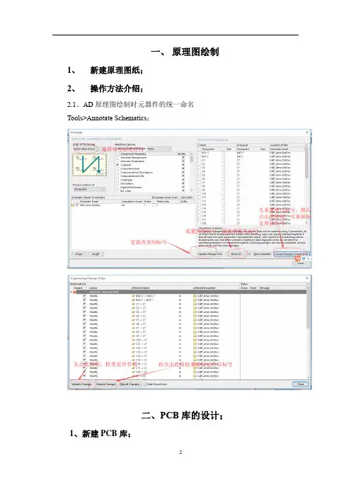
一、原理图绘制1、新建原理图纸;2、操作方法介绍;2.1、AD原理图绘制时元器件的统一命名Tools>Annotate Schematics;二、PCB库的设计;1、新建PCB库;File—New—Library—PCB Library;2、操作方法介绍;2.1、找坐标原点快捷键:crtl +end;2.2、背后网格及单位修改方法:Options—library Options 打开如下画面;2.3、打开原理图库面板;右下角:PCB—PCB Library; 2.4、米制和英制切换:(1)快捷键:Ctrl+Q;(2)如下:2.4 层的隐藏方法如下:2.5、画元件轮廓所用层:(1)顶层:Top Overlay(黄色);(2)底层:bottom Overlay;2.6、封装名称修改方法:2.7 焊盘对齐方法;右击选择Align;2.8、从现有PCB中生产PCB库方法;菜单Design-Make PCB Library3、绘制注意事项;3.1、绘制焊盘的长度比给定长度长1mm左右;3.2、穿孔时,外径一般可设置为内径的2倍左右(内径手册决定,外侧即是焊盘)4、封装向导绘制封装方法4.1、打开封装向导:Tools—component Wizard;三、原理图库的设计;1、操作方法介绍;1.1、操作界面背景修改方法:双击边界;1.2、引脚参数设计如下:四、集成库的设计;五、PCB绘制1、画完原理图之后需做的事:(1):Tools——Annotate Schematics…——(更新元器件的名称)(2):Compile Document Sheet1.SchDoc(编译原理图,之后点击右下角System——message打开检查是否有编译错误和警告。
)2、原理图到更新PCB步骤:(1)新建PCB.pcbdoc,(注意建立后要先保存,否则无法更新成功。
)(2)编译Compile PCB project…(3)Update PCB Document PCB…(4)PCB——PCB,(PCB 编辑目录)(5)PCB——Board insight(微观视图)(6)规则检查:tools——Design rule check(7)tools——Teardrops(8)view——Board insight——toggle insight lens (放大镜,兼显示器件信息)(9)edit——change 可更改器件属性。

一、概述安装AD:1、准备镜像文件和虚拟光驱,。
用虚拟光驱打开镜像文件2、免licence:crack解压缩,将它复制到安装目录下,覆盖已有的打开AD帮助:help菜单home快捷菜单:1、定制自己的菜单:指定toolbar,从commands选定命令拖动到toolbar中;打开此图,选中要删除的命令右击delete。
2、系统设置文件存放自选,库文件默认:中英转换:系统设置不更新:备份:快捷键:,菜单面板:,3、窗口切换:右到左ctrl+tab;由左到右ctrl+shift+tab同时平行显示两个窗口:,返回一个垂直显示:新窗口打开:右击标题栏,同时打开多个窗口:关闭窗口回复初始状态:二、抗干扰设计原则:三、原理图设计:选择project:添加文件:以上几步等同于:打开已有工作空间:对原理图操作:右击——,remove!(从workpace 关闭)=delete(硬盘删除)从其他软件导入:import wizard,缩放图纸大小:1、ctrl+鼠标滑轮滚动2、先按住ctrl+按住右键+上下拖鼠标3、pageup/pagedown 4、按下鼠标中键+上下移动5、移动位置:按右键移动以上可更改:Grid设置:view——单位选择:view——项目菜单:项目打包:规则设置:测距离::依次为:信号线,总线,信号树,总线端口,网络标号,地,电源,元器件……画图快捷方式:排列元器件:放置常用元器件:电源端口:放置仿真符号:设置grid正反步进,可视栅格等:页与页的前进后退:设置原理图:= = D+O(带下划线的大写字母)= = 双击边界区域= = 右击Sheet options默认即可,Parameters 全局变量,units 英制与米制。
设置:断线工具:,在设置原理图绘制:添加库:1、2、选择库:1、2、(常用)3、选择后选择元器件:1、在空白处输入名称2、将鼠标放在元器件名称上,再输入要查找元器件名称3、首先,然后再空白处输入名称Ps:1、,sch中选components2、,都可选3、,不知道元器件在哪个库里选libraries on path或选择自动查找封装所在库,在下一个对话框选择,最后4、搜索帮助放置元器件:1、直接拖到原理图中2、双击3、4、,然后选择放置器件信息提示:删除元器件:1、选中+delete 2、+选择要删除的元器件3、E+D移动元器件:选中+画图:单片机库:电源+滤波电容连接:按住ctrl拖动可延长连线:(drag)等同于按M键后选择= = M+D复制元器件:1、选择后按住shift拖动2、选择后ctrl+c3、选中+edit+(选中+ctrl+R/ctrl+D)编辑元器件属性:1、选中后再次单击2、快速双击后网络标号的连接:数字地与模拟地连接:总线:,总线入口:,起名:1、2、Ps:中括号与两个点不可少元器件编号:1、2、3、单击4、验证更改:最后重新编号:,然后重新编译。
2009-3-11学习笔记 (2)1、电路原理图设计流程 (2)2、添加组件库: (2)3、通过错误报告中叙述的错误类型可以修改在原理图的错误。
(2)4、[Error] has no driver (3)2009-3-12学习笔记 (3)1、关于从sch到pcb的方法: (3)2、关于从pcb文档导出制造输出的方法: (3)3、在Altium Designer 中进行混合信号功能仿真: (3)4、在Altium Designer 中进行信号完整性分析, (3)5、FPGA (4)6、如何在Altium Designer 中运用查找编辑集体整批修改功能 (4)7、如何在Altium Designer 6 中快速生成库: (4)8、如何在Altium Designer 6 的PCB 中添加各种不同字体大小的汉字字符: (4)9、pcb和pcb,sch和sch图之间可以直接复制、粘贴、剪切等 (4)10、新建的库可以通过“器件库/器件库/已经安装/安装/ (4)11、电路原理图(sch)中的元器件名称需要修改, (4)12、V+F获得最佳视觉效果;P+W启动绘制导线命令。
(5)13、制作电路的I/O 口: (5)14、改变管脚的长度: (5)15、PCB 电路板设计的流程 (5)16、集成库的创建: (5)2009-3-13笔记 (6)1、将PCB文件中的网格改为点阵的方法: (6)2、手绘SCH和PCB图,并入库的方法: (6)3、项目、元件库、剪切板等可以从右下状态栏system (6)2009-3-14学习笔记 (6)1、如何在现有的集成库中完成器件修改: (6)2、如何新建一个集成库: (7)3、如何将原Protel99se 的器件库导入到Altium Designer 的Protel 中: (7)3、AD6 的库档转换成99se 的格式 (8)2009-3-17学习笔记 (8)1、什么是SMD 焊盘: (8)2009-3-18学习笔记 (8)1、DXP 2004 Signal PinSignal_C1_1[0] has no driver 问题的解决方法 (8)2、project等菜单被关闭后,将可以在操作界面的右下角System 中点击重新打开。
Altium Designer概述1、Altium designer 是澳大利亚Altium公司出品的集成开发环境。
调出home主页view》home,主页提供了一些快捷菜单,AD10界面是在Task那里。
recently opend。
最近打开的项目和文件(AD6.9版本,AD10是在Recent Items)device management and connections设备管理和链接(针对FPGA设计)configure配置documentation library文件库2、软件本身自带的教程在help里,里边的教程最详细,最权威。
查看帮助文档help》knowledge center或者在任何环境下按f1,会直接弹出帮助文档,在这里,采用上下文敏感的方式,在右上角环形尖头,autoupdate current help topic自动更新当前帮助主题,就是说他的帮助主题会随着你当前内容而变化,绿色的箭头(两个绿色的箭头,一个前进一个后退)右边的黑三角单击一下选择其他帮助选项。
3、home》knowledge base(AD10已更换菜单位置)是一个在线知识库,关于这个软件问题的集合。
user forums 用户论坛4、用户化菜单编辑,在home page里configure》costomize the user interface resources,或者在菜单栏右键》costomize,然后就可以自己定制菜单,选中要定制的选项直接拖到菜单栏就行,例如help》knowledge center 直接拖到菜单栏。
想删除的话先点击出来costomize,然后在菜单栏选中要删除的选项,右键delete。
5、在configure设备里,右边key documentation实际上都是每一个对应一个介绍信息,或者说是一个操作过程,里边都有。
configure第三个setupthe user interface是设置个人喜好。
2010年9月3日星期五:1、新建一个PCB工程,所谓的PCB就是Print circuit board(印刷电路板)的缩写。
里面包含原理图文件,所以不想Protel那样新建工程。
2、文件隶属于工程,工程隶属于工作台。
如下图图1--文件隶属关系3、F1,是帮助快捷键,里面有关于Altium Designer的具体帮助介绍PDF4、项目打包:工程——存档,然后里面就是把项目、工程树、还有工作台压缩打包。
很方便。
视频位置:3.原理图设计初步a.avi 第45分钟5、常用工程参数项设置:在菜单工程里最后一项。
6、网格改变:就是连线时的步进距离,快捷键G可以实现,在左下角可观察到节点在1、5、10mil之间切换。
7、打破线:用于切断部分连接线路,在编辑里面,快捷键:E—W 。
TAB键改变属性。
8、改变连线走向角度:shift+space 为45°和任意角度改变。
2010年9月7日9、LM系列是TI公司的:即德州仪器,如LM358,在找元件库的时候用10、想用99SE打开时,就把文件保存为schematic binary 4.0形式。
2010年9月8日11给工程添加现成的文件原理图和PCB图:右键单击工程名字,第二项有“添加现有的文件到工程”点击即可。
12、利用现成的库来做自己想要的库元件:很方便(包括PCB库封装也可以这样)在库元件编辑的窗口下,点击“打开”,选择要挑选的原理图库文件,然后打开,点击“摘取源文件”打开库元件后,选择自己想要的元件复制到自己创建的元件库中,进行编辑即可。
13、保存:右键点击“工程”,在里面点击“全部保存”。
14、快捷键V—F:适合所有对象最大化。
2010年9月9日15、设置封装库元件中心点:该中心点将直接影响放元件时鼠标在元件周围的位置,一般设为中心就行了。
编辑——设置参考——中心。
16、查看是否所有的元件都进行了封装:工具——封装管理器,一个一个查看。
17、元件对齐:在原理图中或者在PCB布线图中,都能用Shift+鼠标左键,来选取元件,然后在编辑里面选择对齐方式。
altium_designer学习笔记--自己总结1:move:ctrl+移动(即拖动键盘)drag: 直接移动或按m键进行选择2:选中,按住shift,然后拖动,即可实现复制。
4:header是插针,又叫接口、电感:inductor、蜂鸣器:buzzer、三极管:NPN5:databus[0..7]:databus是总线的名字,一定要有中括号,中括号中的表示总线中线的个数,可以是0..7,也可以是3..9。
6:网路标号的最后一位是数字的话,他会自动增加。
7:工具--注解,即可自动注释。
8:分层次的设计的两种方法:从上而下或从下而上。
实际上是两个交互进行的。
设计完编译之后,进行design--同步图纸入口与端口检查。
9:库的设计:库分为原理图库和PCB库。
10:隐藏的引脚接到GND上,那么在图中地的网络标号必须是GND。
GND的引脚类型为Power.也可以将引脚类型都定义为passive,包括GND和VCC,但会对规则检查有影响。
11. 原理图库的元件属性要鼠标指着元件并按F1时打开对应的文档,名字应为HelpURL,值应为地址\文件名.文件类型。
如:HelpURL,C:\Readme.txt12.要出现字母上有一横杆,则在每个字母后面加个反斜杠。
R\e\s\e\t\13.ctrl+end 定位到pcb library的原点。
14.0.1mm=4mil.即1mil=0.025mm. ctrl+q 在英制与米制之间切换。
inch是英寸的意思,1inch=1000mil.按g可选择栅格大小。
正常pcb中引脚长度比实际最长的长1mm~1.5mm或50mil。
要注意算两个焊盘中心之间的距离时要把加长的1mm或50mil留出来。
即在原来的基础上直接加上一个延长的距离。
15:只选Components :只能看到原理图库和集成库只选Footprints : 只能看到PCB库和集成库16:板子:单面板、双面板、多面板双面板分顶层和底层(2层信号层,0层电源层)。