SN74LVC1GU04DBV资料
- 格式:pdf
- 大小:119.48 KB
- 文档页数:8
SN74LVC1GU04
SINGLE INVERTER
SCES215B – APRIL 1999 – REVISED AUGUST 1999
1POST OFFICE BOX 655303 •
DALLAS, TEXAS 75265DEPIC™ (Enhanced-Performance Implanted
CMOS) Submicron Process
DUnbuffered Output
DI
off Feature Supports Partial-Power-Down
Mode Operation
DSupports 5-V V
CC Operation
DPackage Options Include Plastic
Small-Outline Transistor (DBV, DCK)
Packages
description
This single inverter is designed for 1.65-V to 5.5-V V
CC operation.
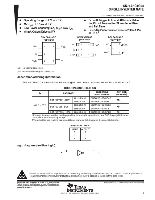
The SN74LVC1GU04 contains one inverter with an unbuffered output, and performs the Boolean function Y = A.
This device is fully specified for partial-power-down applications using I
off. The I
off circuitry disables the outputs,
preventing damaging current backflow through the device when it is powered down.
The SN74LVC1GU04 is characterized for operation from –40°C to 85°C.
FUNCTION TABLE
INPUT
AOUTPUT
Y
HL
LH
logic symbol†
†This symbol is in accordance with ANSI/IEEE Std 91-1984 and IEC Publication 617-12.2
AY4
1
logic diagram (positive logic)
AY24PRODUCT PREVIEW
Copyright © 1999, Texas Instruments IncorporatedPRODUCT PREVIEW information concerns products in the formative or
design phase of development. Characteristic data and other
specifications are design goals. Texas Instruments reserves the right to
change or discontinue these products without notice.Please be aware that an important notice concerning availability, standard warranty, and use in critical applications of
TexasInstruments semiconductor products and disclaimers thereto appears at the end of this data sheet.
EPIC is a trademark of Texas Instruments Incorporated.DBV OR DCK PACKAGE
(TOP VIEW)
1
2
35
4NC
A
GNDV
CC
Y
NC – No internal connection元器件交易网www.cecb2b.comSN74LVC1GU04
SINGLE INVERTER
SCES215B – APRIL 1999 – REVISED AUGUST 1999
2POST OFFICE BOX 655303 •
DALLAS, TEXAS 75265absolute maximum ratings over operating free-air temperature range (unless otherwise noted)†
Supply voltage range, V
CC –0.5 V to 6.5 V. . . . . . . . . . . . . . . . . . . . . . . . . . . . . . . . . . . . . . . . . . . . . . . . . . . . . . . . .
Input voltage range, V
I (see Note 1) –0.5 V to 6.5 V. . . . . . . . . . . . . . . . . . . . . . . . . . . . . . . . . . . . . . . . . . . . . . . . .
Output voltage range, V
O (see Notes 1 and 2) –0.5 V to V
CC + 0.5 V. . . . . . . . . . . . . . . . . . . . . . . . . . . . . . . . . .
Input clamp current, I
IK (V
I < 0) –50 mA. . . . . . . . . . . . . . . . . . . . . . . . . . . . . . . . . . . . . . . . . . . . . . . . . . . . . . . . . . .
Output clamp current, I
OK (V
O < 0) –50 mA. . . . . . . . . . . . . . . . . . . . . . . . . . . . . . . . . . . . . . . . . . . . . . . . . . . . . . . .
Continuous output current, I
O ±50 mA. . . . . . . . . . . . . . . . . . . . . . . . . . . . . . . . . . . . . . . . . . . . . . . . . . . . . . . . . . . . .
Continuous current through V
CC or GND ±100 mA. . . . . . . . . . . . . . . . . . . . . . . . . . . . . . . . . . . . . . . . . . . . . . . . . .
Package thermal impedance, θ
JA (see Note 3):DBV package 347°C/W. . . . . . . . . . . . . . . . . . . . . . . . . . . . . . .
DCK package 389°C/W. . . . . . . . . . . . . . . . . . . . . . . . . . . . . . .
Storage temperature range, T
stg –65°C to 150°C. . . . . . . . . . . . . . . . . . . . . . . . . . . . . . . . . . . . . . . . . . . . . . . . . . .
†Stresses beyond those listed under “absolute maximum ratings” may cause permanent damage to the device. These are stress ratings only, and
functional operation of the device at these or any other conditions beyond those indicated under “recommended operating conditions” is not
implied. Exposure to absolute-maximum-rated conditions for extended periods may affect device reliability.
NOTES:1.The input negative-voltage and output voltage ratings may be exceeded if the input and output current ratings are observed.
2.The value of VCC is provided in the recommended operating conditions table.
3.The package thermal impedance is calculated in accordance with JESD 51.
recommended operating conditions
MINMAXUNIT
VCCSupplyvoltageOperating1.655.5
Supply voltage
Data retention only1.5V
VCC = 1.65 V to 1.95 V0.65 ×VCC
IHHighlevelinputvoltageVCC = 2.3 V to 2.7 V1.7
VHigh-level input voltage
VCC = 2.7 V to 3.6 V2V
VCC = 4.5 V to 5.5 V0.7 ×VCC
VCC = 1.65 V to 1.95 V0.35 ×VCC
VILLowlevelinputvoltageVCC = 2.3 V to 2.7 V0.7
Low-level input voltage
VCC = 2.7 V to 3.6 V0.8V
VCC = 4.5 V to 5.5 V0.3 ×VCC
VIInput voltage05.5V
VOOutput voltage0VCCV
VCC = 1.65 V–4
VCC = 2.3 V–8
IOHHigh-level output currentVCC = 2.7 V–12mA
VCC = 3 V–24
VCC = 4.5 V–32
VCC = 1.65 V4
VCC = 2.3 V8
IOLLow-level output currentVCC = 2.7 V12mA
VCC = 3 V24
VCC = 4.5 V32
VCC = 1.8 V ± 0.15 V, 2.5 V ± 0.2 V20