MJE182中文资料
- 格式:pdf
- 大小:54.77 KB
- 文档页数:4
DCDC驱动电路设计规范2002年05月30日发布2002年05月30日实施艾默生网络能源有限公司前言本规范于2002.05.30首次发布。
本规范起草单位:研发业务管理部、一次电源开发部本规范执笔人:茹永刚本规范主要起草人:茹永刚、方旺林、吴建华、周代文、张华健、张强本规范标准化审查人:林攀本规范批准人:方强本规范修改记录:更改信息登记表目录摘要 (5)缩写词/关键词/解释 (5)1.来源 (5)2.适用范围 (5)3.规范满足的技术指标(特征指标) (5)4.详细电路图................... (5)5.工作原理简介 (6)6.设计、调试要点 (6)7.局部PCB版图(可选项)................. .. (7)8.元器件明细表(详见附录)................................. . (7)9.设计实例 (7)10.附录 (9)附录1.元器件明细表 (9)附录2.应用反例(可选项) (9)摘要本规范介绍了一种常用的MOSFET驱动线路,该电路适用于全桥、半桥等互补对称驱动电路(双正激线路同名端需更改),可以有效的消除由于MOSFET米勒效应引起的误导通。
线路简单成本较低。
关键词米勒效应、导通时间、关断时间缩略词解释一来源本规范中的电路来源于H5415Z模块的实际应用,已经通过大批量运行得到验证,二适用范围该单元电路可用于一般的有双管驱动需求的整流模块中,如一次电源新50A整流模块、新25A整流模块、100A整流模块等等。
三规范满足的技术指标(特征指标)驱动在新50A中的使用指标为:——工作频率:80K——驱动电压:12.5V——驱动功率:1.23W(DC/DC管子采用IRFP460A)四详细的电路图图1 H5415Z驱动线路图五工作原理简介在桥式等有上下管存在的线路中,当上下管中的1只管导通时,另一管的VDS会迅速上升到较高的电压,此时由于mosfet结电容的存在,未导通管的GS间结电容会被充电(即米勒效应),当VGS高到一定程度时,该管导通,即出现上下管直通现象。

深圳市核达中远通电源技术有限公司SHENZHEN HOLDLUCK-ZYT POWER SUPPLY TECHNOLOGY CO., LTD.通孔插装元器件焊孔、焊盘设计工艺规范WI-EN-***版本:A/0分发号:1.0目的:规范元器件焊孔、焊盘设计,满足可制造性要求。
2.0适用范围:通孔插装元器件的焊孔、焊盘设计。3.0内容3.1定义3.1.1引脚直径:若无特殊说明,指圆形引脚的直径,或者指方形(含扁形)引脚截面的对角线长度,用d表示,如图3.1.1(a)、图3.1.1(b)所示。
3.1.2方形(或扁形)引脚截面尺寸:用w表示引脚宽度,用t表示引脚厚度,如图3.1.1(b)所示。
当方形引脚的宽厚比w/t大于2时称为扁形引脚。
3.1.3焊孔直径:圆形焊孔直径,用d1表示,如图3.1.1(c)所示。
3.1.4焊盘直径:圆形焊盘直径,用D表示,如图3.1.1(c)所示。
3.1.5椭圆(或方形)焊盘长度:用L表示,如图3.1.1(d)所示。
3.1.6椭圆(或方形)焊盘宽度:用W表示,如图3.1.1(d)所示。
图3.1.1(b) 方形(或扁形)引脚元器件元件(c) 圆形焊孔及焊盘(d) 圆形焊孔及椭圆(或方形)焊盘3.2 焊孔3.2.1一般情况下,焊孔直径d1按表3.2.1选取: 表3.2.1面板取下限。
注2:在仅有有限的几个插装元件,多数元件为贴装元件的情况下,有可能使用到 通孔回流焊工艺,比如模块针脚的焊接。
3.2.2脚距精度较高,且定位要求也较高的元器件,如输入、输出插座等,焊孔直径等于引脚直径加上0.15~0.2mm 。
3.2.3 方形引脚焊孔:3.2.3.1 w >2.5mm 时,设计为方焊孔(圆角R 为0.3~0.35mm,防止圆角影响插装),方焊孔尺寸如图3.2.3.1所示。
3.2.3.2 w <2 mm 时,设计为圆孔,焊孔直径d1=d+0.15~0.25mm, d 为引脚截面对角线长。
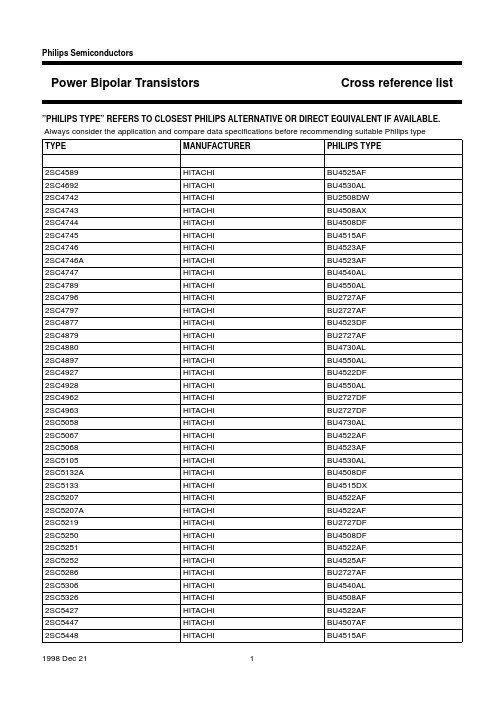
Power Bipolar Transistors Cross reference list”PHILIPS TYPE” REFERS TO CLOSEST PHILIPS ALTERNATIVE OR DIRECT EQUIVALENT IF AVAILABLE. Always consider the application and compare data specifications before recommending suitable Philips typeTYPE MANUFACTURER PHILIPS TYPE2SC4589HITACHI BU4525AF2SC4692HITACHI BU4530AL2SC4742HITACHI BU2508DW2SC4743HITACHI BU4508AX2SC4744HITACHI BU4508DF2SC4745HITACHI BU4515AF2SC4746HITACHI BU4523AF2SC4746A HITACHI BU4523AF2SC4747HITACHI BU4540AL2SC4789HITACHI BU4550AL2SC4796HITACHI BU2727AF2SC4797HITACHI BU2727AF2SC4877HITACHI BU4523DF2SC4879HITACHI BU2727AF2SC4880HITACHI BU4730AL2SC4897HITACHI BU4550AL2SC4927HITACHI BU4522DF2SC4928HITACHI BU4550AL2SC4962HITACHI BU2727DF2SC4963HITACHI BU2727DF2SC5058HITACHI BU4730AL2SC5067HITACHI BU4522AF2SC5068HITACHI BU4523AF2SC5105HITACHI BU4530AL2SC5132A HITACHI BU4508DF2SC5133HITACHI BU4515DX2SC5207HITACHI BU4522AF2SC5207A HITACHI BU4522AF2SC5219HITACHI BU2727DF2SC5250HITACHI BU4508DF2SC5251HITACHI BU4522AF2SC5252HITACHI BU4525AF2SC5286HITACHI BU2727AF2SC5306HITACHI BU4540AL2SC5326HITACHI BU4508AF2SC5427HITACHI BU4522AF2SC5447HITACHI BU4507AF2SC5448HITACHI BU4515AFPower Bipolar Transistors Cross reference listTYPE MANUFACTURER PHILIPS TYPE2SD2293HITACHI BU4505DX2SD2294HITACHI BU4505AX2SD2295HITACHI BU2508DW2SD2296HITACHI BU4508AX2SD2297HITACHI BU2508DW2SD2298HITACHI BU4508AX2SD2299HITACHI BU4505DF2SD2300HITACHI BU4508DF2SD2301HITACHI BU4508AF2SD2311HITACHI BU4508AF2SD2381HITACHI BU4505AF2SC5440MATSUSHITA BU4525AX2SC5456MATSUSHITA BU4530AL2SC5478MATSUSHITA BU2727AX2SC5513MATSUSHITA BU4522AX2SC5514MATSUSHITA BU4523AX2SC5515MATSUSHITA BU4530AL2SC5516MATSUSHITA BU4540AL2SD1391MATSUSHITA BU4508AX2SD1439MATSUSHITA BU4506DX2SD1440MATSUSHITA BU4505DX2SD1441MATSUSHITA BU4507DX2SD1479MATSUSHITA BU5052SD1541MATSUSHITA BU4506DF2SD1575MATSUSHITA BU4504AF2SD1576MATSUSHITA BU4505AF2SD1577MATSUSHITA BU4508AF2SD1632MATSUSHITA BU4507DF2SD1663MATSUSHITA BU4508AF2SD1727MATSUSHITA BU505DF2SD1728MATSUSHITA BU4505DX2SD1729MATSUSHITA BU4507DX2SD1730MATSUSHITA BU4507DX2SD1731MATSUSHITA BU2520DW2SD1732MATSUSHITA BU4523DW2SD1734MATSUSHITA BU505F2SD1735MATSUSHITA BU505F2SD1736MATSUSHITA BU4505AF2SD1737MATSUSHITA BU4507AF2SD1738MATSUSHITA BU4508AF2SD1739MATSUSHITA BU4522AFPower Bipolar Transistors Cross reference listTYPE MANUFACTURER PHILIPS TYPE2SD1844MATSUSHITA BU505DF2SD1845MATSUSHITA BU4505DF2SD1846MATSUSHITA BU4507DF2SD1847MATSUSHITA BU4508DF2SD1848MATSUSHITA BU4522DF2SD1849MATSUSHITA BU4523DF2SD1850MATSUSHITA BU4523AF2SD2001MATSUSHITA BU505F2SD2057MATSUSHITA BU4523DF2SD2310MATSUSHITA BU505F2SD2329MATSUSHITA BU4507AF2SD2330MATSUSHITA BU4523AF2SD2354MATSUSHITA BU4523AW2SD2367MATSUSHITA BU4504DX2SD2368MATSUSHITA BU4506AX2SD2369MATSUSHITA BU4506DX2SD2370MATSUSHITA BU4507AX2SD2371MATSUSHITA BU4508DX2SD2372MATSUSHITA BU4507AX2SD2373MATSUSHITA BU4508AX2SD2510MATSUSHITA BU4506DX2SD2511MATSUSHITA BU4506AX2SD2512MATSUSHITA BU4508DX2SD2513MATSUSHITA BU4508AX2SD2514MATSUSHITA BU4523DX2SD2515MATSUSHITA BU4523AX2SD2521MATSUSHITA BU2708DX2SD2523MATSUSHITA BU2720DXBU508MOTOROLA BU508AWBU508A MOTOROLA BU508AWBU508AD MOTOROLA BU508DWBUH100MOTOROLA“BUJ105A, BUJ106A”BUH150MOTOROLA BUJ106ABUH50MOTOROLA BUJ303ABUL146MOTOROLA BUJ105ABUL146F MOTOROLA BUJ105AXBUL147MOTOROLA BUJ105ABUL147F MOTOROLA BUJ105AXBUL44MOTOROLA BUJ101ABUL44F MOTOROLA BUJ101AXBUL45MOTOROLA BUJ103APower Bipolar Transistors Cross reference listTYPE MANUFACTURER PHILIPS TYPEBUL45F MOTOROLA BUJ103AXMJD13003MOTOROLA BUJ101MJE13003MOTOROLA BUJ101MJE13005MOTOROLA“PHE13005, BUJ103A”MJE13007MOTOROLA BUJ105AMJE13009MOTOROLA BUJ106AMJE16004MOTOROLA“BUJ202A, BUJ204A”MJE16106MOTOROLA BUJ105AMJE18002MOTOROLA“BUJ202A, BUJ301A”MJE18004MOTOROLA“BUJ202A, BUJ303A”MJE18006MOTOROLA“BUJ204A, BUJ303A”MJE18008MOTOROLA“BUJ205A, BUJ304A”MJE18009MOTOROLA“BUJ205A, BUJ304A”MJE18204MOTOROLA BUJ403AMJE18206MOTOROLA BUJ403AMJF13007MOTOROLA BUJ105AXMJF13009MOTOROLA BUJ106AXMJF16212MOTOROLA BU4525AFMJF18002MOTOROLA“BUJ202AX, BUJ301AX”MJF18004MOTOROLA“BUJ202AX, BUJ303AX”MJF18006MOTOROLA“BUJ202AX, BUJ303AX”MJF18008MOTOROLA“BUJ205AX, BUJ304AX”MJF18009MOTOROLA“BUJ205AX, BUJ304AX”MJF18204MOTOROLA BUJ403AXMJF18206MOTOROLA BUJ403AXMJH16212MOTOROLA BU4525AWMJW16212MOTOROLA BU4525AWBUT11A PHILIPS“BUT11AI, BUJ202A, BUJ303A”BUT11AF PHILIPS“BUT11XI, BUJ202AX, BUJ303AX”BUT11AX PHILIPS“BUT11XI, BUJ202AX, BUJ303AX”BUT12A PHILIPS“BUJ204A, BUJ304A”BUT12AF PHILIPS“BUJ204AX, BUJ304AX”BUT12AX PHILIPS“BUJ204AX, BUJ304AX”BUT18A PHILIPS“BUJ204A, BUJ303A, BUJ304A”BUT18AF PHILIPS“BUJ204AX, BUJ303AX, BUJ304AX”BUT18AX PHILIPS“BUJ204AX, BUJ303AX, BUJ304AX”BUT211PHILIPS“BUJ103A, BUJ204A”BUT211X PHILIPS“BUJ103AX, BUJ204AX”BUW14PHILIPS“BUJ202, BUJ301”BUW84PHILIPS“BUJ101, BUJ202”BUW85PHILIPS“BUJ202, BUJ301”Power Bipolar Transistors Cross reference listTYPE MANUFACTURER PHILIPS TYPEBUX84PHILIPS“BUJ101A, BUJ202A”BUX84F PHILIPS“BUJ101AX, BUJ202AX”BUX85PHILIPS“BUJ202A, BUJ301A”BUX85F PHILIPS“BUJ202AX, BUJ301AX”BUX86P PHILIPS“BUJ101, BUJ202”BUX87P PHILIPS“BUJ202, BUJ301”BU508ADF SAMSUNG BU508DWBU508AF SAMSUNG BU508AXBU508DF SAMSUNG BU508DXBU508F SAMSUNG BU508AXKSC2333SAMSUNG BUJ101AKSC2335SAMSUNG BUJ105AKSC2335F SAMSUNG BUJ105AXKSC2518SAMSUNG BUJ103AKSC2752SAMSUNG BUJ101KSC5020SAMSUNG BUJ301AKSC5021SAMSUNG BUJ303AKSC5021F SAMSUNG BUJ303AXKSC5027SAMSUNG BU1706AKSC5027F SAMSUNG BU1706AXKSC5029SAMSUNG BU1706AKSC5030SAMSUNG BU1706AKSC5030F SAMSUNG BU1706AXKSC5039SAMSUNG BUJ103AKSC5039F SAMSUNG BUJ103AXKSC5321SAMSUNG BUJ303AKSC5321F SAMSUNG BUJ303AXKSC5338SAMSUNG“BUJ202A, BUJ204A”KSC5338F SAMSUNG“BUJ202AX, BUJ204AX”KSD5060SAMSUNG BU505DKSD5061SAMSUNG BU4505DXKSD5062SAMSUNG BU4507DXKSD5064SAMSUNG BU505KSD5065SAMSUNG BU4505AXKSD5066SAMSUNG BU4507AXKSD5070SAMSUNG BU4504DXKSD5071SAMSUNG BU4505DXKSD5072SAMSUNG BU4507DXKSD5074SAMSUNG BU4504AXKSD5075SAMSUNG BU4505AXKSD5076SAMSUNG BU4507AXPower Bipolar Transistors Cross reference listTYPE MANUFACTURER PHILIPS TYPEKSD5078SAMSUNG BU4522AXKSD5080SAMSUNG BU4522DXKSD5086SAMSUNG BU4508DXKSD5088SAMSUNG BU4522AXKSD5089SAMSUNG BU2520AWKSD5090SAMSUNG BU2520DWKSE13004SAMSUNG BUJ103AKSE13005SAMSUNG“PHE13005, BUJ103A”KSE13005F SAMSUNG BUJ103AXKSE13006SAMSUNG BUJ105AKSE13007SAMSUNG BUJ105AKSE13007F SAMSUNG BUJ105AXKSE13008SAMSUNG BUJ106AKSE13009SAMSUNG BUJ106AKSE13009F SAMSUNG BUJ106AX2SC4023SANKEN BU2520AW2SC5002SANKEN BU4522AF2SC5003SANKEN BU4522DF2SC3681SANYO BU4507DX2SC3682SANYO BU2508DW2SC3683SANYO BU2520DW2SC3685SANYO BU4507AX2SC3686SANYO BU4508AX2SC3687SANYO BU2520AW2SC3688SANYO BU4530AW2SC3894SANYO BU4507AX2SC3895SANYO BU4508AX2SC3896SANYO BU4522AX2SC3897SANYO BU4530AL2SC3995SANYO BU4530AL2SC3996SANYO BU4530AL2SC3997SANYO BU4540AL2SC3998SANYO BU4540AL2SC4122SANYO BU4507DX2SC4123SANYO BU4508DX2SC4124SANYO BU4522DX2SC4291SANYO BU4507DX2SC4292SANYO BU2508DW2SC4293SANYO BU4507DX2SC4294SANYO BU4508DX2SC4435SANYO BU4508AXPower Bipolar Transistors Cross reference listTYPE MANUFACTURER PHILIPS TYPE2SC4436SANYO BU4515AX2SC4437SANYO BU4508AX2SC4438SANYO BU4515AX2SC4769SANYO BU4508DX2SC4770SANYO BU4508AX2SC4890SANYO BU4540AL2SC4891SANYO BU4540AL2SC4923SANYO BU4522AX2SC4924SANYO BU4522AX2SC5041SANYO BU2708DX2SC5042SANYO BU2708AX2SC5043SANYO BU2727DX2SC5044SANYO BU2727AX2SC5045SANYO BU4730AL2SC5046SANYO BU4730AL2SC5296SANYO BU4508DX2SC5297SANYO BU4522AX2SC5298SANYO BU4522AX2SC5299SANYO BU4522AX2SC5302SANYO BU4530AL2SD1396SANYO BU505D2SD1397SANYO BU4505DX2SD1398SANYO BU4507DX2SD1399SANYO BU2508DW2SD1400SANYO BU5052SD1401SANYO BU4505AX2SD1402SANYO BU4507AX2SD1403SANYO BU4508AX2SD1649SANYO BU4504DX2SD1650SANYO BU4505DX2SD1651SANYO BU4507DX2SD1652SANYO BU4508DX2SD1653SANYO BU4504AX2SD1654SANYO BU4505AX2SD1655SANYO BU4507AX2SD1656SANYO BU4508AX2SD1677SANYO BU4508AX2SD1709SANYO BU2508DW2SD1710SANYO BU4508AX2SD1711SANYO BU4508DX2SD1876SANYO BU4504DXPower Bipolar Transistors Cross reference listTYPE MANUFACTURER PHILIPS TYPE2SD1877SANYO BU4505DX2SD1878SANYO BU4507DX2SD1879SANYO BU4508DX2SD1880SANYO BU4522DX2SD1881SANYO BU4525DX2SD1882SANYO BU4504AX2SD1883SANYO BU4505AX2SD1884SANYO BU4507AX2SD1885SANYO BU4508AX2SD1886SANYO BU4522AX2SD1887SANYO BU4525AX2SD2251SANYO BU4508AX2SD2252SANYO BU4508AXBU508SANYO BU508AWBU508A SANYO BU508AWBU508D SANYO BU508DW2SC3162SHINDENGEN BUJ103A2SC3163SHINDENGEN BUJ105A2SC4051SHINDENGEN BUJ202A2SC4052SHINDENGEN BUJ202AX2SC4053SHINDENGEN BUJ204A2SC4054SHINDENGEN BUJ204AX2SC4055SHINDENGEN BUJ205A2SC4056SHINDENGEN BUJ205AX2SC4230SHINDENGEN BU1706A2SC4231SHINDENGEN BU1706AX2SC4233SHINDENGEN BU1706A2SC4234SHINDENGEN BU1706AX2SC4310SHINDENGEN BU1706A2SC4311SHINDENGEN BU1706AXT2V80HFX SHINDENGEN BU1706AT3V40F3SHINDENGEN BUJ103AT3V45FX SHINDENGEN BUJ202AT3V80HFX SHINDENGEN BU1706AT5V45FX SHINDENGEN BUJ204AT6V40F3SHINDENGEN BUJ105AT6V80HDT SHINDENGEN BU1706AT8V45FX SHINDENGEN BUJ205ATP2V80HFX SHINDENGEN BU1706AXTP3V45FX SHINDENGEN BUJ202AXTP3V80HFX SHINDENGEN BU1706AXPower Bipolar Transistors Cross reference listTYPE MANUFACTURER PHILIPS TYPETP5V45FX SHINDENGEN BUJ204AXTP6V80HDT SHINDENGEN BU1706AXTP8V45FX SHINDENGEN BUJ205AX2SD1577FI ST (SGS-THOMSON)BU4508AXBU208A ST (SGS-THOMSON)BU4508AXBU208D ST (SGS-THOMSON)BU4508AXBU505ST (SGS-THOMSON)BU505BU505ST (SGS-THOMSON)BU1706ABU508ST (SGS-THOMSON)BU508AWBU508A ST (SGS-THOMSON)BU508AWBU508AD ST (SGS-THOMSON)BU508DWBU508AFI ST (SGS-THOMSON)BU508AXBU508AXI ST (SGS-THOMSON)BU4508AZBU508D ST (SGS-THOMSON)BU508DWBU508DFI ST (SGS-THOMSON)BU508DXBU508DXI ST (SGS-THOMSON)BU4508DZBU508FI ST (SGS-THOMSON)BU508AXBUF405ST (SGS-THOMSON)BUJ204ABUH1015ST (SGS-THOMSON)BU4540AWBUH1015HI ST (SGS-THOMSON)BU4540ALBUH1215ST (SGS-THOMSON)BU4540AWBUH315ST (SGS-THOMSON)BU4506AXBUH315D ST (SGS-THOMSON)BU4506DXBUH315DXI ST (SGS-THOMSON)BU4506DZBUH315XI ST (SGS-THOMSON)BU4506AZBUH415DXI ST (SGS-THOMSON)BU4507DZBUH417ST (SGS-THOMSON)BU2708AXBUH515ST (SGS-THOMSON)BU4508AXBUH515D ST (SGS-THOMSON)BU4508DXBUH515DX1ST (SGS-THOMSON)BU4508DZBUH515FP ST (SGS-THOMSON)BU4508DZBUH515XI ST (SGS-THOMSON)BU4508AZBUH517ST (SGS-THOMSON)BU2720AXBUH517D ST (SGS-THOMSON)BU2720DXBUH615ST (SGS-THOMSON)BU4522AXBUH615D ST (SGS-THOMSON)BU4522DXBUH715ST (SGS-THOMSON)BU4523AXBUL128ST (SGS-THOMSON)BUJ103ABUL128FP ST (SGS-THOMSON)BUJ103AXBUL138ST (SGS-THOMSON)“BUJ103A, BUJ202A”BUL138FP ST (SGS-THOMSON)“BUJ103AX, BUJ202AX”Power Bipolar Transistors Cross reference listTYPE MANUFACTURER PHILIPS TYPEBUL216ST (SGS-THOMSON)BU1706ABUL26ST (SGS-THOMSON)BUJ103ABUL310ST (SGS-THOMSON)BUJ303ABUL310PI ST (SGS-THOMSON)BUJ303AXBUL381ST (SGS-THOMSON)“BUJ103A, BUJ202A”BUL382ST (SGS-THOMSON)“BUJ103A, BUJ202A”BUL410ST (SGS-THOMSON)“BUJ204A, BUJ304A”BUL416ST (SGS-THOMSON)BU1706ABUL48ST (SGS-THOMSON)“BUJ105A, BUJ204A”BUL510ST (SGS-THOMSON)BUJ304ABUL57ST (SGS-THOMSON)BUJ105ABUL57PI ST (SGS-THOMSON)BUJ105AXBUL59ST (SGS-THOMSON)BUJ204ABUL67ST (SGS-THOMSON)BUJ106ABUL810ST (SGS-THOMSON)BUJ305ABUL87ST (SGS-THOMSON)BUJ106ABULK26ST (SGS-THOMSON)BUJ103BULK381ST (SGS-THOMSON)“BUJ103, BUJ202”BULK382ST (SGS-THOMSON)“BUJ103, BUJ202”BULT118ST (SGS-THOMSON)BUJ101S2000AFI ST (SGS-THOMSON)BU4508AXS2000AXI ST (SGS-THOMSON)BU4508AZSGSF323ST (SGS-THOMSON)“BUJ202A, BUJ303A”SGSF343ST (SGS-THOMSON)“BUJ204A, BUJ304A”ST13003ST (SGS-THOMSON)BUJ101ST13005ST (SGS-THOMSON)“PHE13005, BUJ103A”ST13007ST (SGS-THOMSON)BUJ105AST1802HI ST (SGS-THOMSON)BU4507AXST1803DHI ST (SGS-THOMSON)BU4507DXST2001HI ST (SGS-THOMSON)BU4515AXTHD200FI ST (SGS-THOMSON)BU4525AXTHD215HI ST (SGS-THOMSON)BU4522AXTHD218DHI ST (SGS-THOMSON)BU4507DXTHD277HI ST (SGS-THOMSON)BU4507AXTHD300ST (SGS-THOMSON)BU4540AWBU508TELEFUNKEN BU508AWBU508A TELEFUNKEN BU508AWBU508AD TELEFUNKEN BU508DWBU508D TELEFUNKEN BU508DWBU508DR TELEFUNKEN BU508DWBU705TELEFUNKEN BU505Power Bipolar Transistors Cross reference listTYPE MANUFACTURER PHILIPS TYPEBU908TELEFUNKEN BU4506AX2SC3884A TOSHIBA BU4508AX2SC3885A TOSHIBA BU4515AX2SC3886A TOSHIBA BU4522AX2SC3887A TOSHIBA BU4508AX2SC3888A TOSHIBA BU4515AX2SC3889A TOSHIBA BU2520AW2SC3892A TOSHIBA BU4508DX2SC3893A TOSHIBA BU4522DX2SC4288A TOSHIBA BU4540AL2SC4289A TOSHIBA BU4540AL2SC4290A TOSHIBA BU4550AL2SC4531TOSHIBA BU4523DX2SC4532TOSHIBA BU4730AL2SC4542TOSHIBA BU4525AX2SC4560TOSHIBA BU4525AW2SC4757TOSHIBA BU4515AX2SC4758TOSHIBA BU4522AX2SC4759TOSHIBA BU4525AX2SC4761TOSHIBA BU2722AX2SC4762TOSHIBA BU4508DX2SC4763TOSHIBA BU4522DX2SC4764TOSHIBA BU4507DX2SC4765TOSHIBA BU2708DX2SC4766TOSHIBA BU2720DX2SC4806TOSHIBA BU2708AX2SC4830TOSHIBA BU4508AX2SC4916TOSHIBA BU4508DX2SC5048TOSHIBA BU4523AX2SC5129TOSHIBA BU4515AX2SC5142TOSHIBA BU4550AL2SC5143TOSHIBA BU2727DX2SC5148TOSHIBA BU4508AX2SC5149TOSHIBA BU4508DX2SC5150TOSHIBA BU2727AX2SC5331TOSHIBA BU4530AL2SC5332TOSHIBA BU2727AW2SC5339TOSHIBA BU4508DX2SC5386TOSHIBA BU4515AX2SC5387TOSHIBA BU4522AX2SC5404TOSHIBA BU4522AXPower Bipolar Transistors Cross reference listTYPE MANUFACTURER PHILIPS TYPE2SC5421TOSHIBA BU4530AL2SC5422TOSHIBA BU4730AL2SC5445TOSHIBA BU4540AL2SD1425TOSHIBA BU505D2SD1426TOSHIBA BU4506DX2SD1427TOSHIBA BU4507DX2SD1428TOSHIBA BU2508DW2SD1429TOSHIBA BU5052SD1430TOSHIBA BU4506AX2SD1431TOSHIBA BU4507AX2SD1432TOSHIBA BU4508AX2SD1433TOSHIBA BU2520AW2SD1543TOSHIBA BU4504AX2SD1544TOSHIBA BU4506AX2SD1545TOSHIBA BU4507AX2SD1546TOSHIBA BU4508AX2SD1547TOSHIBA BU4522AX2SD1553TOSHIBA BU4504DX2SD1554TOSHIBA BU4506DX2SD1555TOSHIBA BU4507DX2SD1556TOSHIBA BU4508DX2SD2089TOSHIBA BU4504DX2SD2095TOSHIBA BU4507DX2SD2125TOSHIBA BU4508DX2SD2253TOSHIBA BU2720DX2SD2348TOSHIBA BU4522DX2SD2349TOSHIBA BU4523DX2SD2428TOSHIBA BU2725DW2SD2454TOSHIBA BU2720DX2SD2498TOSHIBA BU4508AX2SD2499TOSHIBA BU4508DX2SD2500TOSHIBA BU4523AX2SD2539TOSHIBA BU4522DX2SD2550TOSHIBA BU2708DX2SD2551TOSHIBA BU2720DX2SD2552TOSHIBA BU2720DX2SD2553TOSHIBA BU2725DX2SD818TOSHIBA BU5052SD819TOSHIBA BU4506AX2SD820TOSHIBA BU4507AX2SD821TOSHIBA BU4508AXPower Bipolar Transistors Cross reference listTYPE MANUFACTURER PHILIPS TYPE2SD822TOSHIBA BU2520AW2SD868TOSHIBA BU505D2SD869TOSHIBA BU4506DX2SD870TOSHIBA BU4507DX2SD871TOSHIBA BU2508DWS2000TOSHIBA BU4508AXS2000A TOSHIBA BU4508AXS2000AF TOSHIBA BU4508AXS2000F TOSHIBA BU4508AXS2055TOSHIBA BU2508DWS2055A TOSHIBA BU2508DWS2055AF TOSHIBA BU4508DXS2055F TOSHIBA BU4508DXS2818TOSHIBA BU2508DWS2818A TOSHIBA BU2508DWBUD600VISHAY/ SILICONIX BUJ101BUD620VISHAY/ SILICONIX BUJ103BUD630VISHAY/ SILICONIX“BUJ103, BUJ105”BUD636A VISHAY/ SILICONIX“BUJ202, BUJ303”BUD86VISHAY/ SILICONIX“BUJ101, BUJ202”BUD87VISHAY/ SILICONIX“BUJ202, BUJ301”BUF620VISHAY/ SILICONIX BUJ103ABUF630VISHAY/ SILICONIX“BUJ103A, BUJ105A”BUF636A VISHAY/ SILICONIX“BUJ202A, BUJ303A”BUF640A VISHAY/ SILICONIX“BUJ204A, BUJ303A”BUF642VISHAY/ SILICONIX BUJ204ABUF644VISHAY/ SILICONIX BUJ105ABUF646A VISHAY/ SILICONIX“BUJ204A, BUJ304A”BUF650VISHAY/ SILICONIX“BUJ105A, BUJ106A”BUF654VISHAY/ SILICONIX BUJ106ABUF742VISHAY/ SILICONIX BUJ303ABUF744VISHAY/ SILICONIX BUJ105ATD13002VISHAY/ SILICONIX BUJ101TD13003VISHAY/ SILICONIX BUJ101TD13004VISHAY/ SILICONIX BUJ103TD13005VISHAY/ SILICONIX BUJ103TE13004VISHAY/ SILICONIX“PHE13005, BUJ103A”TE13005VISHAY/ SILICONIX“PHE13005, BUJ103A”TE13008VISHAY/ SILICONIX BUJ106ATE13009VISHAY/ SILICONIX BUJ106A。
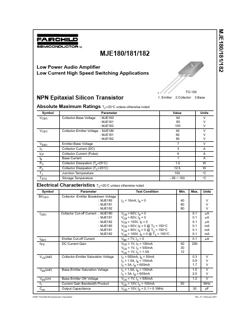
MJE180/181/182MJE180/181/182MJE180/181/182TRADEMARKSThe following are registered and unregistered trademarks Fairchild Semiconductor owns or is authorized to use and is not intended to be an exhaustive list of all such trademarks.DISCLAIMERFAIRCHILD SEMICONDUCTOR RESERVES THE RIGHT TO MAKE CHANGES WITHOUT FURTHER NOTICE TO ANY PRODUCTS HEREIN TO IMPROVE RELIABILITY, FUNCTION OR DESIGN. FAIRCHILD DOES NOT ASSUME ANY LIABILITY ARISING OUT OF THE APPLICATION OR USE OF ANY PRODUCT OR CIRCUIT DESCRIBED HEREIN;NEITHER DOES IT CONVEY ANY LICENSE UNDER ITS PATENT RIGHTS, NOR THE RIGHTS OF OTHERS.LIFE SUPPORT POLICYFAIRCHILD’S PRODUCTS ARE NOT AUTHORIZED FOR USE AS CRITICAL COMPONENTS IN LIFE SUPPORT DEVICES OR SYSTEMS WITHOUT THE EXPRESS WRITTEN APPROVAL OF FAIRCHILD SEMICONDUCTOR INTERNATIONAL.As used herein:1. Life support devices or systems are devices or systems which, (a) are intended for surgical implant into the body,or (b) support or sustain life, or (c) whose failure to perform when properly used in accordance with instructions for use provided in the labeling, can be reasonably expected to result in significant injury to the user.2. A critical component is any component of a life support device or system whose failure to perform can be reasonably expected to cause the failure of the life support device or system, or to affect its safety or effectiveness.PRODUCT STATUS DEFINITIONS Definition of TermsDatasheet Identification Product Status DefinitionAdvance InformationFormative or In Design This datasheet contains the design specifications for product development. Specifications may change in any manner without notice.PreliminaryFirst ProductionThis datasheet contains preliminary data, andsupplementary data will be published at a later date.Fairchild Semiconductor reserves the right to make changes at any time without notice in order to improve design.No Identification Needed Full ProductionThis datasheet contains final specifications. Fairchild Semiconductor reserves the right to make changes at any time without notice in order to improve design.Obsolete Not In ProductionThis datasheet contains specifications on a product that has been discontinued by Fairchild semiconductor.The datasheet is printed for reference information only.ACEx™Bottomless™CoolFET™CROSSVOLT™DOME™E 2CMOS™EnSigna™FACT™FACT Quiet Series™FAST ®FASTr™GlobalOptoisolator™GTO™HiSeC™ISOPLANAR™MICROWIRE™OPTOLOGIC™OPTOPLANAR™PACMAN ™POP™PowerTrench ®QFET™QS™QT Optoelectronics™Quiet Series™LILENT SWITCHER ®SMART START™SuperSOT™-3SuperSOT™-6SuperSOT™-8SyncFET™TinyLogic™VCX™UHC™。

MJE13001 是小功率高压高速开关三极管,典型应用:荧光灯电子镇流器。
它采用TO-92 封装,管脚排列如图:MJE13001 主要参数:集电极-基极最高耐压VCBO=500V 集电极-发射极最高耐压VCEO=400V 发射极-基极最高耐压VEBO=9V 集电极电流IC=0.3A耗散功率PC=7W结温Tj=150℃贮藏温度TSTG=-50~150℃直流放大系数HFE=8~403DD13001 是硅NPN 型小功率开关三极管,主要用于节能灯电子镇流器、手机充电器等开关电源电路。
3DD13001 具有击穿电压高、反向漏电流小、开关速度快、饱和压降低、高温性能好等特点。
采用TO-251 封装的3DD13001 管脚排列如图:1脚:基极;2脚:集电极;3脚:发射极3DD13001 主要参数:集电极最大耗散功率PCM=1.2W (Tamb=25℃)集电极最大允许电流ICM=0.2A集电极-基极反向击穿电压BVCBO=600V 集电极-发射极反向击穿电压BVCEO=400V 发射极-基极反向击穿电压BVEBO=7V结温Tj=150℃贮藏温度TSTG=-55~150℃直流放大系数=8~40MJE13002 是高压高速开关三极管,国产同类型号为3DD13002。
它主要用于电子节能灯、日光灯电子镇流器,以及其它开关电路中。
MJE13002(3DD13002)采用TO-126 封装的外形尺寸和管脚排列如图:MJE13002(3DD13002)主要参数VCBO=600VVCEO=400VVEBO=7VIC=1APC=1.2WTj=150℃TSTG=-55~150℃ICBO=100μAIEBO=100μAHFE=10~40VCE(sat) =0.5VVBE(sat) =1.0VfT=4MHzTf=0.6μsMJE13003 是主要用于节能灯及荧光灯电子镇流器的高反压大功率开关三极管,硅NPN 型,采用TO-126 封装,它的外形和管脚排列如下:MJE13003 主要参数集电极-基极电压VCBO 700 V 集电极-发射极电压VCEO 400 V 发射极-基极电压VEBO 9V集电极电流IC 2.0 A 集电极耗散功率PC 40 W 最高工作温度Tj 150 °C 贮存温度Tstg -65-150 °C集电极-基极截止电流ICBO (VCB=700V) 100 μA集电极-发射极截止电流ICEO (VCE=400V,IB=0) 250 μA集电极-发射极电压VCEO (IC=10mA,IB=0) 400 V发射极-基极电压VEBO (IE=1mA,IC=0) 9 V 直流电流放大倍数5~403DD13005 是高反压大功率开关三极管,硅材料NPN 型,平面扩散工艺制造,开关速度快,耐压高。
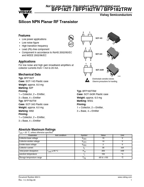
BFP182T / BFP182TW / BFP182TRWDocument Number 85013Rev. 1.5, 05-Sep-08Vishay Semiconductors134Not for new design, this product will be obsoleted soonSilicon NPN Planar RF TransistorFeatures•Low power applications •Low noise figure•High transition frequency•Lead (Pb)-free component•Component in accordance to RoHS 2002/95/EC and WEEE 2002/96/ECApplicationsFor low noise and high gain broadband amplifiers at collector currents from 1 mA to 20 mA.Mechanical DataTyp: BFP182TCase: SOT-143 Plastic case Weight: approx. 8.0 mg Marking: 82P Pinning:1 = Collector,2 = Emitter,3 = Base,4 = Emitter Typ: BFP182TWCase: SOT-343 Plastic case Weight: approx. 6.0 mg Marking: W82Pinning:1 = Collector,2 = Emitter,3 = Base,4 = EmitterTyp: BFP182TRWCase: SOT-343R Plastic case Weight: approx. 6.0 mg Marking: WSG Pinning:1 = Collector,2 = Emitter,3 = Base,4 = EmitterAbsolute Maximum RatingsT amb = 25°C, unless otherwise specifiedParameterT est conditionSymbol Value Unit Collector-base voltage V CBO 15V Collector-emitter voltage V CEO 10V Emitter-base voltage V EBO 2V Collector current I C 35mA T otal power dissipation T amb ≤ 60°CP tot 200mW Junction temperature T j 150°C Storage temperature rangeT stg-65 to +150°C元器件交易网 2Document Number 85013Rev. 1.5, 05-Sep-08BFP182T / BFP182TW / BFP182TRWVishay Semiconductors Maximum Thermal Resistance1)on glass fibre printed board (25 x 20 x 1.5) mm 3 plated with 35 μm CuElectrical DC CharacteristicsT amb = 25°C, unless otherwise specifiedParameterTest condition Symbol Value Unit Junction ambient1)R thJA450K/WParameterTest conditionSymbol MinTyp.Max Unit Collector-emitter cut-off current V CE = 15 V , V BE = 0I CES 100μA Collector-base cut-off current V CB = 10 V , I E = 0I CBO 100nA Emitter-base cut-off current V EB = 1 V , I C = 0I EBO 1μA Collector-emitter breakdown voltageI C = 1 mA, I B = 0V (BR)CEO 10V Collector-emitter saturation voltageI C = 15 mA, I B =1.5 mAV CEsat 0.10.4VDC forward current transfer ratio V CE = 6 V , I C = 5 mAh FE 5090150V CE = 8 V , I C = 20 mAh FE100BFP182T / BFP182TW / BFP182TRWDocument Number 85013Rev. 1.5, 05-Sep-08Vishay Semiconductors3Electrical AC CharacteristicsT amb = 25°C, unless otherwise specifiedPackage Dimensions in mmParameterT est conditionSymbol MinT yp.MaxUnit T ransition frequencyV CE = 6 V , I C = 5 mA, f = 500 MHzf T 5.5GHz V CE = 8 V , I C = 20 mA, f = 500 MHzf T 7.5GHz Collector-base capacitance V CB = 10 V, f = 1 MHz C cb 0.3pF Collector-emitter capacitance V CE = 8 V , f = 1 MHz C ce 0.2pF Emitter-base capacitance V EB = 0.5 V, f = 1 MHzC eb 0.7pF Noise figureV CE = 6 V , I C = 5 mA, Z S = Z Sopt , f = 900 MHzF 1.5dB V CE = 6 V , I C = 5 mA, Z S = Z Sopt , f = 1.75 GHzF 2.0dB Power gainV CE = 8 V , I C = 20 mA, Z S = 50 Ω, Z L = Z Lopt , f = 900 MHzG pe18dBV CE = 8 V , I C = 20 mA, Z S = 50 Ω, Z L = Z Lopt , f = 1.75 GHzG pe12dBT ransducer gainV CE = 8 V , I C = 20 mA, Z 0 = 50 Ω, f = 900 MHz|S 21e |215dB 4Document Number 85013 Rev. 1.5, 05-Sep-08BFP182T / BFP182TW / BFP182TRW Vishay SemiconductorsPackage Dimensions in mmPackage Dimensions in mmBFP182T / BFP182TW / BFP182TRWDocument Number 85013Rev. 1.5, 05-Sep-08Vishay Semiconductors5Ozone Depleting Substances Policy StatementIt is the policy of Vishay Semiconductor GmbH to1.Meet all present and future national and international statutory requirements.2.Regularly and continuously improve the performance of our products, processes, distribution and operating systems with respect to their impact on the health and safety of our employees and the public, as well as their impact on the environment.It is particular concern to control or eliminate releases of those substances into the atmosphere which are known as ozone depleting substances (ODSs).The Montreal Protocol (1987) and its London Amendments (1990) intend to severely restrict the use of ODSs and forbid their use within the next ten years. Various national and international initiatives are pressing for an earlier ban on these substances.Vishay Semiconductor GmbH has been able to use its policy of continuous improvements to eliminate the use of ODSs listed in the following documents.1.Annex A, B and list of transitional substances of the Montreal Protocol and the London Amendments respectively2.Class I and II ozone depleting substances in the Clean Air Act Amendments of 1990 by the Environmental Protection Agency (EPA) in the USA3.Council Decision 88/540/EEC and 91/690/EEC Annex A, B and C (transitional substances) respectively.Vishay Semiconductor GmbH can certify that our semiconductors are not manufactured with ozone depleting substances and do not contain such substances.We reserve the right to make changes to improve technical designand may do so without further notice.Parameters can vary in different applications. All operating parameters must be validated for each customer application by the customer. Should the buyer use Vishay Semiconductors products for any unintended or unauthorized application, the buyer shall indemnify Vishay Semiconductors against all claims, costs, damages, and expenses, arising out of, directly or indirectly, any claim of personaldamage, injury or death associated with such unintended or unauthorized use.Vishay Semiconductor GmbH, P.O.B. 3535, D-74025 Heilbronn, GermanyDocument Number: 91000Revision: 18-Jul-081DisclaimerLegal Disclaimer NoticeVishayAll product specifications and data are subject to change without notice.Vishay Intertechnology, Inc., its affiliates, agents, and employees, and all persons acting on its or their behalf (collectively, “Vishay”), disclaim any and all liability for any errors, inaccuracies or incompleteness contained herein or in any other disclosure relating to any product.Vishay disclaims any and all liability arising out of the use or application of any product described herein or of any information provided herein to the maximum extent permitted by law. The product specifications do not expand or otherwise modify Vishay’s terms and conditions of purchase, including but not limited to the warranty expressed therein, which apply to these products.No license, express or implied, by estoppel or otherwise, to any intellectual property rights is granted by this document or by any conduct of Vishay.The products shown herein are not designed for use in medical, life-saving, or life-sustaining applications unless otherwise expressly indicated. Customers using or selling Vishay products not expressly indicated for use in such applications do so entirely at their own risk and agree to fully indemnify Vishay for any damages arising or resulting from such use or sale. Please contact authorized Vishay personnel to obtain written terms and conditions regarding products designed for such applications.Product names and markings noted herein may be trademarks of their respective owners.元器件交易网。
CONTENTSTITLE PAGE CONTENTS········································page 1 of10 RECORD OF REVISIONS····························page 1 of10 GENERAL DESCRIPTION····························page 2 of10 FUNCTION LAYOUT·································page 2 of10 FEATURES·········································page 3 of10 INTERFACE DEFINITION····························page 5 of10 CONTROLLER DIMENSIONS·························page 9 of10KEY & IR BOARD SYSTEM SCHEMATIC··············page 9 of10 OPERATION REQUIREMENT·························page 10 of10RECORD OF REVISIONSREVISION NO. DATE PAGE DESCRIPTION1. GENERAL DESCRIPTIONMST182VG V6.0 is a multi-purpose LCD controller, it is suitable Asia market.It is designed to support FULL HD LCD panel.MST182VG V6.0 can support PC-RGB,HDMI,AV,YPBPR,USB, VGA,TV signal input.It can also support Earphone output.Note:The specification of the board includes the description of all functions. Therefore,our clients can select the functions which they require to produce the board.But the specification can be introduced universally.2. FUNCTION LAYOUTThe following all pictures are a reference only. Please take the actual objects as a standard.Elevation of MST6M182VG V6.0Side Elevation of MST6M182VG V6.03. FEATURESBelow you will find the detailed feature.CHIPSET MST6M182VG MARKET AREA AsiaOSD LANGUAGEEnglish,Chinese,(French,Spanish,Polish,Portuguese,Italian,German,Dutch,Russian)(Option )VIDEO SYSTEM PAL/SECAM,NTSC(Option)SOUND SYSTEM BG ,DK ,I, MTV RECEIVE CHANNELATV:200CVBS 1.0Vp-p +/-5% YPbPr / YCbCr 480i 、480p 、576i 、576p 、720p 、1080i 、1080pFormat Up to 1920*1080@60HZPC-RGBColor 16bit, 24bit, 32bitVIDEO INPUTHDMI 480i 、480p 、576i 、576p 、720p 、1080i 、1080p Build-in powersupply 5V,5VS,12V or only 12V (Option )To panel 5V,12V POWERManage Low power consumable mode: standby ≤0.5WPC-RGB YESAUDIO INPUTAV/YPbPr Audio InputYESEXPANSIONFUNCTIONUSB YESPANELRESOLUTIONSSupport up to 10-bit dual LVDS FULL HD panel interface KEY FUNCTIONS CH-,CH+,MENU,VOL-,VOL+,SOURCE,ON/OFFAUDIO OUTPUT2*8 W @ 8Ω COMB FILTER3D DE-INTERLACE3D WEAK SIGNAL ENHANCEMENTYES NOISE REDUCTION3D NICAM/A2, TELETEXT,BTSC,CC,VCHIPYES TV Input 1 IEC 75 Ω PC-RGB Input 1D-SUB 15PIN terminal blue color HDMI Input 3HDMI terminal CVBS Input 1RCA terminal yellow colorYPbPr Input3RCA terminal green color,blue color andred colorYPbPr Audio InputCVBS Audio Input 2*2RCA terminal white color, red colorInput USB 2 USB terminal To Panel Double LVDS 38PIN/2.0 jackSPDIF 1RCA terminal orange colorTERMINALSOutput Earphone Out 1earphone terminal black color USB MULTIMEDIA PLAYBACK FORMAT MEDIA FILE EXTENSIONPicture JPEG 、BMP 、PNG .jpg 、.bmp 、.pngMovieMPEG1、MPEG2、MPEG4、H264、RM 、RMVB 、MOV 、MJPEG 、VC1、Divx 、FLV.avi 、.mpg 、.dat 、.vob 、.div 、.mov 、.mkv 、.rm 、.rmvb 、.mp4、.mjpeg 、ts 、.trp 、.wmv 、.asf 、.flvMusic WMA 、MP3、M4A 、AAC .wma 、.mp3、.m4aFILE TYPE\THE RELEVANT PARAMETERSRESOLUTIONCOMPRESSIONOPTION SUPPORT BOUNDARIES Progressive JPEGResolution Only Support 1024*768Baseline (”standard”) supportJPEG 15360*8640 Baseline optimizedsupporthomochromatism Support16color Support256color Support 16bit Support24bit SupportBMP 9600*640032bit supportNo interlacingSupport PNG 9600*6400InterlacedResolution Only Support 1200*800*Realize that only when you gain the copyright of the corresponding USB functions ,can the above-mentioned USB functions be used. 4. INTERFACE DEFINITIONCN1 ( 13PIN/2.0 ) MAIN POWER SUPPLYNO.SYMBOLDESCRIPTIONELECTRIC CHARACTER1 12VA2 12VA+12V DC Power supply2A+Panel Electric Current +electric Current of extended module 3 GND4 GND5 GND Ground ---6 5V7 5V+5V DC Power supply2A+Panel Electric Current + electricCurrent of extended module 8 5VS +5V DC Power standby 1A 9 PW ON/OFF --- 10 5V 11 5V+5V DC Power supply2A+Panel Electric Current + electricCurrent of extended module 12 GND Ground ---13 GND Ground ---CN2 (5PIN/2.0) DVD POWER SUPPLYNO. SYMBOL DESCRIPTION1 12VIN +12V DC Power supply2 GND Ground3 GND Ground4 5V_DVD DVD +5V DC Power supply5 5V_DVD DVD +5V DC Power supplyCN4( 6PIN/2.0 ) INVERTER INTERFACENO. SYMBOL DESCRIPTION ELECTRIC CHARACTER1 GNDGround ---2 GNDadjustableadjustment 0-5V3 ADJUST Brightness4 ON/OFF Back-light ON/OFF control 5V ,1K ohm output impedance5 12VA +12V DC Power supply INVERTER Power Supply6 12VA +12V DC Power supply INVERTER Power SupplyCN5 (4PIN/2.0) DVD DEBUGGING INTERFACENO. SYMBOL DESCRIPTION1 GND Grounddata2 DVD-TXD Transmitdata3 DVD-RXD ReceiveIR4 DVD_IR DVDCN6 (2PIN/2.0) EXTERNAL MEMC CONTROL I2CNO. SYMBOL DESCRIPTION1 SDA I2C Master bus for SDA2 SCL I2C Master bus for SCLCN7 (9PIN/2.0) KEY BOARD INTERFACENO. SYMBOL DESCRIPTION1 GND Ground2 CH- CH-keyKey3 CH+ CH+4 MENU MENUKeyKey5 VOL- VOL-Key6 VOL+ VOL+7 GND GroundKey8 SOURCE SOURCEkey9 ON/OFF ON/OFFCN8 (5PIN/2.0) REMOTE RECEIVER INTERFACENO. SYMBOL DESCRIPTION1 GND Groundreceiver2 IR_IN Remote3 LED_G Greenindicatorindicator4 LED_R Red5 IR_VCC +5V DC power supplyCN9 (2*19PIN/2.0) LVDS PANEL INTERFACENO. SYMBOL DESCRIPTION1 VDD Power for panel2 CT mode pin for panel3 VDD Power for panel4 GNDGround5 GND6 GND7 RXO0- LVDS ODD 0- Signal8 RXO0+ LVDS ODD 0+ Signal9 RXO1- LVDS ODD 1- Signal10 RXO1+ LVDS ODD 1+ Signal11 RXO2- LVDS ODD 2- Signal12 RXO2+ LVDS ODD 2+ Signal13 GNDGround14 GND15 RXOC- LVDS ODD Clock- Signal16 RXOC+ LVDS ODD Clock+ Signal17 RXO3- LVDS ODD 3- Signal18 RXO3+ LVDS ODD 3+ Signal19 RXE0- LVDS EVEN 0- Signal20 RXE0+ LVDS EVEN 0+ Signal21 RXE1- LVDS EVEN 1- Signal22 RXE1+ LVDS EVEN 1+ Signal23 RXE2- LVDS EVEN 2- Signal24 RXE2+ LVDS EVEN 2+ Signal25 GND Ground26 GND Ground27 RXEC- LVDS EVEN Clock- Signal28 RXEC+ LVDS EVEN Clock+ Signal29 RXE3- LVDS EVEN 3- Signal30 RXE3+ LVDS EVEN 3+ Signal31 RXE4- LVDS EVEN 4- Signal32 RXE4+ LVDS EVEN 4+ Signal33 RXO4- LVDS ODD 4- Signal34 RXO4+ LVDS ODD 4+ Signal35 SCL SCL36 SDA SDAflag37 3D_FLAG 3Dbrightness adjustment38 PB_ADJUST Back-lightCN10 (4PIN/2.0) DEBUGGING INTERFACENO. SYMBOL DESCRIPTION1 GND Grounddata2 UART-RX Receivedata3 UART-TX Transmit4 +5V_Standby +5V Power supplyCN28 (9PIN/2.0) YPBPR INPUTNO. SYMBOL DESCRIPTION1 Y Y signal input2 GND Ground3 PB PB signal input4 GND Ground5 PR PR signal input6 GND Ground7 R YPBPR right audio input8 GND Ground9 L YPBPR left audio input CN30 (4PIN/2.54) SPEAKER INTERFACENO. SYMBOL DESCRIPTION1 R+ Positive right audio channel out2 R- Negative right audio channel out3 L- Negative left audio channel out4 L+ Positive left audio channel out5. CONTROLLER DIMENSIONSThe dimension is identical to the actual objects.But maybe exist the slight error of measures about 1%.It is allowed in design.6. KEY & IR BOARD SYSTEM SCHEMATICMST6M182VG V6.0 Specification- 10 -7. OPERTION REQUIREMENT· Do not pressed and distorted. · Keep away from static and water. · Relative humidity: ≤80%· Storage temperature:-10~ +60℃ · Operation temperature:0~ +40℃。
E-Panel InstructionsModel: MNE125ST, MNE175ST, MNE250ST, MNE125AL, MNE175AL, MNE250AL,MNE175STS, MNE250STS, MNE125LT, MNE175LT, MNE250LT, MNE125ALT, MNE175ALT, MNE250ALT, MNE125AL PLUS, MNE175AL PLUS, MNE250 PLUSMNE125STM, MNE175STM, MNE250STM, MNE125ALM, MNE175ALM, MNE250ALM, MNE125STMM, MNE175SM, MNE250SMLeft and Right hand 120/240VAC versionsModel Number code:MNE---------------175-----------ST or AL----------------M-240IMPORTANT SAFETY INSTRUCTIONSSAVE THESE INSTRUCTIONS - These instructions contain important safety and operating instructions for MidNite Solar E-Panels.If you do not fully understand any of the concepts, terminology, or hazards outlined in these instructions, please refer installation to a qualified dealer, electrician or installer. These instructions are not meant to be a complete explanation of a renewable energy system.GENERAL PRECAUTIONSWORKING WITH OR IN THE VICINITY OF A LEAD ACID BATTERY, SEALED OR VENTED IS DANGEROUS. VENTED BATTERIES GENERATE EXPLOSIVE GASES DURING NORMAL OPERATION. FOR THIS REASON, IT IS VERY IMPORTANT THAT BEFORE SERVICING EQUIPMENT IN THE VICINITY OF LEAD-ACID BATTERIES YOU REVIEW AND FOLLOW THESE INSTRUCTIONS CAREFULLY.If service or repair should become necessary, contact MidNite Solar Inc. Improper servicing may result in a risk of shock, fire or explosion. To reduce these risks, disconnect all wiring before attempting any maintenance or cleaning. Turning off the inverter will not reduce these risks. Solar modules produce power when exposed to light. When it is not possible to disconnect the power coming from the Photovoltaics by an external means such as a combiner, cover the modules with an opaque material before servicing any connected equipment.Never attempt to charge a frozen battery.When it is necessary to remove a battery, make sure that the battery bank disconnect breaker is in the off position and that the PV breakers, grid breakers and any other sources of power to the inverter are in the off position. Then remove the negative terminal from the battery first.To reduce risk of battery explosion follow these instructions and those published by the battery manufacturer as well as the manufacturer of any additional equipment used in the vicinity of the batteries. Before installing the battery enclosure, read all instructions and cautionary markings in or on any connected electrical equipment.Avoid producing sparks in the vicinity of the batteries when using vented batteries. Provide ventilation to clear the area of explosive gases. Sealed AGM and Gel batteries do not under normal conditions create explosive gases. Be especially cautious when using metal tools. Dropping a metal tool onto batteries can short circuit them. The resulting spark can lead to personal injury or damage to the equipment. Provide ventilation to outdoors from the battery compartment when installing vented batteries such as golf cart T-105 batteries. The addition of a spill tray is also a good idea.Clean all battery terminals. Very high currents are drawn from the batteries; even a small amount of electrical resistance can result in overheating, poor performance, premature failure or even fire.Have plenty of fresh water and soap nearby in case battery acid contacts skin, clothing or eyes. Wear complete eye and clothing protection. Always avoid touching eyes while working near batteries. If battery acid or battery terminal corrosion contacts skin or clothing, wash immediately with soap and water. If acid enters the eyes, immediately flood with cool running water for at least 15 minutes and get medical attention immediately. Baking soda neutralizes battery acid electrolyte. Keep a supply near the batteries.Do not work alone. Someone should be in the range of your voice or close enough to come to your aid when you work with or near electrical equipment.Remove rings, bracelets, necklaces, watches etc. when working with batteries, photovoltaic modules or other electrical equipment. Power from an illuminated photovoltaic array makes a very effective arc welder with dire consequences if one of the welded pieces is on your person.To reduce the risk of injury, connect only deep cycle lead acid type rechargeable batteries. Other types of batteries may leak or burst, causing personal injury or damage.This equipment is NOT intended for use with life support equipment or other medical equipment or devices.It is the responsibility of the installer to verify compliance with all applicable codes.Before making any connections verify that the circuit breakers are in the off position including the inverter breaker. Double check allwiring before applying power.The MidNite Solar E-Panel comes standard with the basic over-current protection and disconnects required to install your renewable energy system. It can also expand to grow as your needs arise.List of features:● Steel or aluminum chassis with all the r equired openings and knock outs to aid in a NEC compliant system installation● Inverter mounts on a unique hinged door to keep the footprint of the system small as possible● Mounting brackets are included to aid in one person installations● Inverter ba ttery breaker, inverter cables and snap in grommets included*● 500 amp / 50mv shunt included for battery monitoring systems● B us bars are included for additional battery plus, PV plus and battery minus wiring● Heavy duty 175 amp AC power distribution bu s bars included● 50 amp AC input disconnect for generator or utility included, pre-wired (15amp MM series) ● 50 amp AC bypass switch for bypassing inverter circuit, pre-wired (15amp MM series)● Mounting bracket to aid in mounting an OutBack MX60 or MidNi te Classic to the side of the E-Panel*● Battery cable cover to enclose cables external to the chassis***● Inverter and charge controller mounting hardware● Rectangular cut outs for mounting a North American GFCI style AC outlet● Cut outs for mounting up to six additional 13mm wide din rail mount breakers and three ¾” wide panel mount breakers for additional circuits such as PV, wind, hydro or AC distribution ● Plastic snap in conduit and fittings from chassis to inverter for AC, BTS and control circu its (OB versions)● ETL listed to UL and CSA standards* inverter cables and charge control bracket omitted on the LT configurations*** LT versions do not have a cable cover, MM series uses the inverter battery terminal capsThe dimensioned chassis drawings above show the location of the conduit knockouts, mounting holes and mounting brackets.✓Knockouts on the top surface are directly in line with ones on the bottom surface for stacking units vertically.✓Knockouts on the lower end of each side are directly in line with each other for stacking horizontally.✓Steel powder coated units are gray textured. Aluminum powder coated units are gloss white.Door ConfigurationThe standard E-Panel comes as a left hand hinged assembly with breakers on the left side and a left hand hinged door. The door will open to the left over the breakers. If for some reason you need the breakers on the left, but the door to open to the right, then you need the optional right hand door. All breakers can be unmounted and reassembled on the right side of the chassis as is explained in this manual. Right hand E-Panels can be built special at the factory for no additional charge. Changing sides in the field is not a simple task! The left hand hinge is standard because the majority of charge controllers need to be mounted to the right side of the E-Panel. See below.1. Apollo T-80 should be a left hand hinge (heatsink is on the right)3. OutBack MF80 should be left hand hinge (No knock out on the right side of chassis)4. MX60 works equally as well on either side5. WX controller works equally as well on either side6 C40/C60 and Tri-star work equally as well on either side7. Blue Sky has the heatsink on the left, so should use a right hand hinge.See E-Panels explained on the MidNite website for exact part numbers of door options and an explanation of each E-Panel platform. E-Panels Explained will further help you in selecting the applicable E-Panel for your application.The installation begins by selecting a wall. All E-Panels are indoor rated and should not be placed outside unless precautions are made to keep rain and moisture off of the system. The wall must have suitable clearance to open the door with inverter attached. It must also have adequate clearance to operate the breakers and outlets that protrude out the sides. The NEC requires 30” clear on the wall. The E -Panel may be located anywhere within this 30 inches, however make sure you have sufficient room to the side to operate the circuit breakers. Some E-Panel installations may have circuit breakers on both sides. The NEC also requires 36 inches free and clear of obstructions in front of the E-Panel. The 36” clear area in front of all electrical panels is to provide a space to fall back into incase of electrical shock. Each E-Panel with its’ inverter will weigh close to 100 pounds so make sure your wall is adequate for this load. The mounting brackets provided will span studs on 16 inch centers. Mount the top bracket as shown at about 64-68 inches off the floor. If stacking two systems vertically, make sure the breakers fall within the NEC guidelines for height, (lowest and highest allowable). Number 10 screws with back up washers will suffice, but ¼” (6mm) hardwar e provides for a better margin of safety.A little pre-planning here will go a long way towards a successful installation. Battery boxplacement and size also need to be thought out for NEC compliance. The remote display should be approximately at eye level when attached to the E-Panel. Some installation photos below show various ways to install your system.You can make life a little easier by installing additional breakers for charge control, the inverter and such while the E-Panel is still lying horizontal on a table. Do as much of the additionalwiring as possible before hanging the E-Panel on the wall. The following pictures show some of the operations that can be done “on the bench” where access is optimal.Field installed breakers should be torqued to 20 inch pounds, then re-torqued after one hour. This is important! Wires cold flow and sometimes loosen up after the initial tightening, so don’t skip this step. E-Bay is a good source for Sturdevant Richmont torque screw drivers if you are an installer.Breakers such as charge control input and output and DC-GFP can be completely wired prior to installation on the wall. Field wiring is done at the PV, AC and DC terminal bus bars.This picture shows the Outback E-Panel mountedwith two MNEPV63 charge control breakersinstalled and an AC and DC MNSPD Surge ProtectorDevice. The upper mounting bracket can be securedto the wall and then the E-Panel chassis hung ontoit using the keyhole slots in the upper back of thechassis.Before mounting the inverter to the chassis andwith the E-Panel mounted on the wall, complete allwiring that will be coming to and going from the E-Panel. The following pictures give you some idea ofwhat to expect.The picture to the right is a Magnum 240V E-Panel.Notice it has an OutBack OBDC-GFP mounted on the leftside of this right hand hinge unit. There are a total of sixdin rail slots available on each E-Panel for customerconfiguration. This installation has two chargecontrollers. You need a breaker in the PV input and onthe DC output of the charge controller. This took up 4din rail slots for this system. The MidNite DC-GFP takesup 2 din rail slots for the 63 amp version and 2 panelmount knock out slots for the 80 amp version. Neitherone of these would work in this case, so the two circuitOutBack GFP was used. It takes up three slots on theblank plate opposite the din rails. Note the green 6AWGneutral to ground bonding wire in this picture. Theneutral to ground bond is required on all systems perNEC. Note that if this were a power back up system on autility connected home, this bonding wire would not beinstalled as it would already be there on the serviceentrance. On off-grid installations thatemploy a sub panel circuit breaker box, you can make this neutral to ground bond in the sub-panel. It is technically better to make this bond closest to the source of power (the E-Panel), but many electrical inspectors will be looking for it in the sub-panel box. It will work just fine in either location, just make sure you have adequate conductor sizes between the E-Panel and the sub-panel. Do not rely on the hinges for grounding the equipment mounted to the door.The picture to the left shows the charge control bracket suppliedin the E-Panel kit. This one is for a left hand hinged unit, so thecharge control bracket is on the right side opposite the din railbreakers.The charge control bracket supplied works with the OutBackMX60, MF80, MidNite Classic and Xantrex WX charge controllers.The Charge control bracket is secured to the E-Panel with 3 #10 x3/8” sheet metal e one more screw to secure the topbracket of charge controller and a 1” close nipple on the side asshown below. Note tha t it takes three 1” locknuts to mount the controller. One lock nut is used in between the E-Panel side and the charge controller side to act as a spacer. It may help to replace the pan head screws on the side plate with flat head screws in some cases to increase clearance.In addition to the 1” close nipple andthree locknuts, you will need plasticthreaded adapters installed on the endsof the metal threaded nipple. Theseadapters protect wires from coming intocontact with the sharp edges of themetal close nipple.Before wiring the charge controller,determine what size wire and breakerswill be required. The breakers are there to protect the wiring, notthe controller!It is very common to use the MidNite 63 amp din rail breakers for this task. Even if the charge controller is only 30 amps, it can be wired using 63 amp breakers. You will need 6AWG wire to go with those breakers though. If using one of the more powerful 80 amp charge controllers, you will need the MNEDC80 panel mount breakers. These mount on the opposite wall from the din rail breakers. 4AWG wire is required to match up with these 80 amp breakers.The flow path for the PV circuit is as follows:1.The PV + wire comes into the E-Panel and attaches to the PV+ busbar2.The PV- comes into the E-Panel and attaches to the shunt busbar. This is for charge controllers thathave a common PV- and battery- connection, (most are this way). Some charge controllers like the Xantrex XW and the Blue Sky must keep thes PV- and battery- circuits separated. The E-Panels have mounting embosses to accommodate a short white busbar to act as an isolated PV-. Use theMNSBBW for the busbar.3.From the PV+ busbar, use the appropriate gauge red wire (THHN) and connect to the PV+ INbreaker. DC breakers have polarity markings. These may be a + sign or a line and load sign.Although the PV circuit has very limited energy available and thus making polarity issues not too critical, it is best to try to get it right. This is where the fun begins.4. The + (line) marking on the breaker would seem to indicate that you should connect the PV+ tothis terminal since the PV+ is the highest potential in the system. Our testing shows this would be correct. The + side of the breaker needs to be connected to the highest potential per the breaker instructions.5.The - side of the PV in breaker goes to the charge controller PV+ input terminal.6.The output of the charge controller is sometimes marked battery+ This terminal is to connect tothe charge controller output breaker. It will not connect to the + or Line side of the breaker.7.The other side of the breaker, + or line connects to the battery plus busbar. This connection isimportant to observe polarity markings. In the event of a charge controller failure, they quite often short internally, which means they are shorting out the battery. If proper polarity is not observed, the breaker may not open and the wiring will burn up.The factory installed red battery plus bus wire is 4AWG, so it is large enough for all breaker sizes.The diagrams above show 63 amp din rail mount breakers. When 80 amp breakers and or DC-GFPare required, those breakers mount on the wall opposite the din rails. Thereare three panel mount breaker slots to accommodate the 80 ampbreakers and DC-GFP. The 80 amp DC-GFP takes up two of the three slots. The third slot will be used for the output of the 80 amp charge controller. The PV input to an 80 amp charge controller could use a 63 amp din rail mount breaker. There is no additional DC-GFP required when using the MidNite Classic controller. The DC-GFP and arc fault protector are built into the Classic controllers.Mounting the inverterThe 6 x 20mm pan head Philips screws for mounting the inverter are taptite (thread forming). Use one of these 6mm screws to pre-tap threads into the steel doors extruded funnel holes. Aluminum doors have press nuts and do not require tapping. Make sure to install all ¼” star washers to bite through the powder coating.One of the best features of the MidNite E-Panel is that one person can do all the lifting.Slip Tab A into Slot B Install inverter cablesInstall the 3.5” bushing as shown protruding up into the inverter side of the door before routing the inverter cables through the door.More tidbits to digestImportant! Torque din rail mount breakers Installing the breaker cover to 20 in lb. Wait one hour and re-torque .Six locations are available for additional 13mm wide breakers. These breakers would normally be field installed for such things as: solar, wind or hydro charge controllers, DC ground fault protector, AC and or DC distribution center and others. Remove the cut outs for the intended breakers. Each 13mm wide breaker requires removal of two cut outs. 17.5mm wide breakers require removal of three cut outs. It is important to torque the terminals to 20 inch pounds. It is highly recommended to go back over all terminations after an hour and also conduct a pull test.Doors installed,plastic conduit installed, wiring complete. Note the battery cable routing. It is important to route cables so the doors close freely without undue force. The left E-Panel battery cables came from above, but could have come fromYou may be surprised that what you thought was a tight connection actually pulls out with little effort. This is caused be a phenomenon called cold flow. Copper is a relatively soft metal and will continue to move under inadequate clamping pressure. A 20 inch pound of torque takes a lot of strength! Use the supplied UL listed plastic 2” x 6” spacers to separate AC and DC breakers if installed on the same din rail. Barriers are required per NEC between AC and DC circuits.MidNite offers 150VDC breakers in 1,2,3,4,5,6,7,8,9,10,12,15,20,30,40,50 and 63 amps. AC breakers are available in 10,15 and 20 amp sizes. Those breakers carry the UL489 and UL489A branch circuit rating. 30 and 50 amp AC breakers are available in UL1077 listed versions, but are not branch circuit rated.For OutBack installations, install the conduit pieces supplied by routing the three wires through the door and conduit before snapping the fittings into place. Snap the top right angle fitting into place first and then the one in the door. Once the length of wire has beenestablished by opening and closing the door, then cut back the three wires as required and hook up to the terminal block. The conduit in the middle of the inverter is for AC wiring. The outer conduit is for remote and battery temp sense wires.Note: Battery cables in a NEC compliant system requires cable listed for use in residential wiring.For installations requiring the OutBack surge arrestor, see pictures below. Note that this surge arrestor is only accommodated on the Stretched OutBack E-Panel.The flex conduit snaps into the sides of the surge arrestor. You will need to get an adapter to go from the 1” conduit hole in the surge arrestor housing to the ¾” flex conduit. These are readily available at your local electrical supply store or Home Depot/Lowes.This basic wiring diagram is mounted on the inside of the hinged door. Elsewhere in these instructions is a slightly expanded version of the E-Panel wiring diagram. There is an AutoCAD version of the expanded wiring diagram at This is provided so that interested parties may download and modify it to tailor their specific system configuration. When stacking two OutBack inverters, it may be required to add the OutBack PSX-240 autotransformer.OutBack and Magnum horizontal stacked systemsE-Panel parts locator, DoorSupplied insulators to achieverequired separation of AC and DCcircuitsE-Panel parts locator, internal Ground to Neutral connectionMagnum MS4448-AE & MS4024-AE system pre-wire with DC-GFPMNE175SM / MNE250SM Samlex E-Panel wiring.MNE175SM Shown.。
DETAILING HINTS❏ 1.Carefully cut the radios and fuel gauges from theinstrument decal included in your T op Flite Cessna kit and attach them to the front of the plastic instrument panel.Attach the remaining instrument decal pieces to scrap balsa or thin cardboard,then glue it to the back of the molded panel.The numbers on this photo apply to the following steps❏2.Carpet may be attached to the floor with 3M #77sprayadhesive.Glue the carpet in position,then cut around the front seat tracks to expose them.T rim the carpet edges to size.❏ 3.Seat and door beading can be made from embroidery“floss”or string.T ack glue a short piece at one end with thin CA,then stretch it to the end of its run.Hold it with tweezers while you CA the floss or string in place.❏4.Seatbelts are cut from 1/4"dressmakers’elastic (included in this kit).One end is threaded through the eye of a large T -pin and spot glued to itself.The pin is inserted through the floor,bent 90degrees and glued to the underside of the floor.The buckles are cut from chrome trim tape or could be made from aluminum foil.❏5.Maps and magazines are made from small pieces of thereal thing.❏6.The cavity on the back side of the control yokes is filled with automotive body filler or epoxy.Before the filler sets-up,insert a 1/8"x 1-1/4"dowel into the center of the yoke.Secure it in position until the filler cures.The dowels are mounted by drilling 1/8"holes through the instrument panel and glued to small scrap wood blocks on the back side.❏7.All knobs and buttons are made from large and smallquilters pins.Insert them through the instrument panel,then bend them 90°on the back side.Cut off the excess close to where the pins are bent,then glue them in position on the back side.❏8.The pull straps on the doors are made from short pieces ofscrap plastic glued in position with CA.Many more details can be added.It’s up to you.A little imagination and craftsmanship is all it takes.Have fun with this project.The results will be well worth the effort.FINAL INSTALLATION❏1.Glue the left and right cabin sides in position.We suggestusing clear silicone sealer as the adhesive because it provides a good bond between wood and plastic.❏2.Slide the floor into position between the sides followed by the aft bulkhead.The floor and aft bulkhead may be glued in position with CA.Glue the seats to the floor with CA after scraping off any paint from the points of contact.❏3.Install the instrument panel using your chosen method.When you take your Cessna 182to the field,try to be gracious in accepting all the praise you will undoubtedly get.Happy flying!PRINTED IN USA.™SCRAPS FROM AROUND YOUR WORKSHOP ❏Stiff paper or index card –for seat pockets ❏Chrome trim tape –for seatbelt buckles ❏Large T -pins –for seatbelt attachmentGETTING STARTEDAssembling and installing your scale cockpit will probably require minor adjustments and “tweaking”to fit your particular model.This is because of variations in building technique,parts alignment and glue fillets that may interfere with proper positioning of the parts.A little patience is all that is required to obtain a good looking installation.Trim parts a little at a time,checking the fit after each adjustment.Remember,you can always remove material,but it’s hard to put it back.❏1.Start by trimming all parts to the embossed “trim lines.”Be sure to leave a 1/8"-3/16"lip around the fuse side panels to provide a gluing surface for the floor and aft e a hobby knife or scissors to “rough cut ”the parts,then sand the parts with a sanding block to straighten the edges.Y ou can evenly sand the edges by simply taping a sheet of 240-grit sandpaper to your workbench.Then work the part in a circular motion while pressing down gently.Cut out the center of each instrument cavity and smooth the edges with sandpaper.NOTE:Save all scraps of smooth plastic (especially from inside the window openings)for later use.❏2.Carefully remove the bottom portions of the front and rearseat backs as shown in the photo.The side “tabs”will be used to attach the seat backs to the lower sections.❏3.Refer to the exploded drawing on the following page to seehow the parts will fit together.Without using glue,(and in the following order),fit the sides,floor,aft bulkhead and instrumentpanel into the fuselage cavity.Y ou will need to cut the top edge of the sides to fit around the wing blocks and top cabin cross-member as shown in the e the underside of the rear window frame and also the side windows for reference whenhard balsa.The servo cover could be folded back for access to the servos or it could be made completely removable –your option.❏5.When you are satisfied with the fit of the primary cabinparts,remove them from the model and set them aside until it’s time to paint.ASSEMBLE THE SEATS❏1.Cut several 1/4"x 1"strips of plastic from the flat scrap material you saved earlier.These will be used to create gluing tabs for the seats.Glue three strips inside the bottom halves of both front seats (protruding half way over the edge)as shown.Glue four strips inside the bottom of the rear seat .❏2.Glue two or three strips to the inside of the three seatback cushions.❏3.Insert the tabs of the rear seat back into the bottom half of the seat,then apply a piece of masking tape to the joint.The seat back should angle toward the rear of the cabin by a few degrees.Glue the seat back in position by “wicking”a few drops of thin CA into the joint from the back side.Remove the tape after the CA has cured.❏4.T ape the rear seat cushions to the bottom half of the seat ata couple of places.When the two halves are aligned,use thin CA to glue the parts e the same technique to add the seat back cushions.❏5.Assemble the two front seats the same way as the rear seat.❏e plastic model seam putty or automotive body filler tocover all of the joints.When the filler has cured,wet sand it smooth with 340or 400-grit sandpaper.❏7.Seat back pockets can be made from index cards or stiff paper glued into position with thin CA.PAINTING AND DETAILING❏1.Before painting,thoroughly clean the parts with rubbing alcohol,then allow them to dry completely.❏2.Paint the parts with paint compatible with styrene.For the best results,use spray paint.Do not use T op Flite LustreKote as it is not compatible with styrene.If adding “carpeting,”paint only the embossed seat tracks before installing the fabric.。
MJE172MJE182
COMPLEMENTARY SILICON POWER TRANSISTORS
s SGS-THOMSON PREFERRED SALESTYPES s
COMPLEMENTARY PNP - NPN DEVICES
DESCRIPTION The MJE172 (PNP type) and MJE182 (NPN type)are silicon epitaxial planar, complementary transistors in Jedec SOT-32 plastic package, they are designed for low power audio amplifier and low current, high speed switching applications.
®
September 1998
ABSOLUTE MAXIMUM RATINGS
1/4
THERMAL DATA
ELECTRICAL CHARACTERISTICS (T case = 25 o
C unless otherwise specified)
For PNP type voltage and current values are negative.
MJE172 - MJE182
MJE172 - MJE182
Information furnished is believed to be accurate and reliable. However, STMicroelectronics assumes no responsibility for the consequences of use of such information nor for any infringement of patents or other rights of third parties which may result from its use. No license is granted by implication or otherwise under any patent or patent rights of STMicroelectronics. Specification mentioned in this publication are subject to change without notice. This publication supersedes and replaces all information previously supplied. STMicroelectronics products are not authorized for use as critical components in life support devices or systems without express written approval of STMicroelectronics.
The ST logo is a registered trademark of STMicroelectronics © 1998 STMicroelectronics – Printed in Italy – All Rights Reserved
STMicroelectronics GROUP OF COMPANIES
Australia - Brazil - Canada - China - France - Germany - Italy - Japan - Korea - Malaysia - Malta - Mexico - Morocco - The Netherlands -Singapore - Spain - Sweden - Switzerland - Taiwan - Thailand - United Kingdom - U.S.A.
.
MJE172 - MJE182。