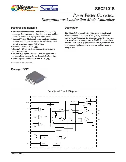
Power Factor CorrectionDiscontinuous Conduction Mode ControllerSSC2101SContinued on the next page…DescriptionThe SSC2101S is a controller IC intended to implement a Discontinuous Conduction Mode (DCM) interleavedPower Factor Correction (PFC) circuit. Using the two-phase interleaved control incorporated in this IC, it is possible to achieve a low cost, high performance PFC system with low input / output ripple currents, low noise, and few external components.Features and Benefits▪ Interleaved Discontinuous Conduction Mode (DCM) operation: low peak current, low ripple current, and low noise; for medium- to high-power applications▪ Constant V oltage Mode control: no auxiliary windings required on inductors because of the built-in arithmetic circuit; achieves a simple PFC system • Maximum on-time: 15 μs (typ)▪ Built-in Soft Start function: reduces stress on power devices at startup▪ Built-in High Speed Response (HSR): suppression of output voltage changes during dynamic load transients ▪ Error Amplifier reference voltage: 3.5 V (typ)Functional Block DiagramPackage: SOP8SOP8+–Terminal List TableName Number Function1COMP Error Amplifier output and phase compensation terminal 2VIN AC mains rectified voltage monitoring input terminal3VFB Feedback control terminal, input for: Constant Voltage Mode control signal, Overvoltage Protection signal, and Open Loop Detection signal 4VCC IC power supply input terminal 5OUT2Gate drive 2 output terminal 6GND IC ground terminal7OUT1Gate drive 1 output terminal8ISPeak current detection signal input terminal12348765IS OUT1GND OUT2COMP VIN VFB VCC Pin-out Diagram▪ Protection Functions▫ Soft Overvoltage Protection (SOVP): output voltage reduction ▫ Output Overvoltage Protection (OVP): gate drive on/off on a pulse-by-pulse basis, with auto-restart▫ Overcurrent Protection (OCP): dual-level OCP, with auto-restart▫ Output Open Loop Detection (OLD): switching operation stop and transition to standby mode▫ Open Terminal Protection (OTP): switching operation stop or output voltage reduction, during open condition on VFB, VIN, or IS terminals▫ Thermal Shutdown (TSD): auto-restart with hysteresisSelection GuidePart NumberSSC2101SFeatures and Benefits (continued)Absolute Maximum Ratings * T A = 25°C unless otherwise specifiedCharacteristicsSymbol NotesTerminals Rating Unit VCC Terminal Voltage V CC 4 – 6−0.3 to 30A COMP Terminal Voltage V COMP 1 – 6−0.3 to 5.5A VFB Terminal Voltage V FB 3 – 6−0.3 to 5.5V VFB Terminal Current I FB 3 – 6−1 to 1mA VIN Terminal Voltage V IN 2 – 6−0.3 to 5.5V VIN Terminal Current I IN 2 – 6−1 to 1mA IS Terminal Voltage V IS 8 – 6−16.0 to 5.5V IS Terminal Current I IS 8 – 6−1.75 to 1mA OUT2 Terminal Voltage V OUT2 5 – 6−0.3 to 30V OUT1 Terminal Voltage V OUT17 – 6−0.3 to 30V Operating Frame Temperature T FOP –−40 to 85°C Storage Temperature T stg –−40 to 125°C Junction TemperatureT j–−40 to 125°C*Current polarity is defined relative to the IC: sink as positive, source as negative.ELECTRICAL CHARACTERISTICS Valid at T A = 25°C, unless otherwise specifiedCharacteristics Symbol Test Conditions Terminals Min.Typ.Max.Unit Power Supply Start-up OperationVCC Operation Start Voltage V CC(ON) 4 – 610.811.612.4V VCC Operation Stop Voltage V CC(OFF) 4 – 69.810.611.4V VCC Undervoltage Lockout Hysteresis V CC(HYS) 4 – 60.8 1.0 1.2V VCC Circuit Current in Pre-operation I CC(OFF) 4 – 6–40100μA VCC Circuit Current in Operation I CC(ON) 4 – 6–11.015.0mA VCC Circuit Current During OVP I CC(OVP) 4 – 6–8.010.0mA VCC Circuit Current During Standby I CC(Standby) 4 – 6–100200μA Oscillator OperationMaximum On-Time t ONMAX7 – 6141516μsOUT1 to OUT2 On-Time Matching t RATIO 5 – 67 – 6−505%OUT1 to OUT2 Phase Difference∆PHASE 5 – 67 – 6170180190deg.Protection OperationVFB Output Open Loop Stop Voltage V FB(OLDL) 3 – 60.460.500.54V VFB Output Open Loop Start Voltage V FB(OLDH) 3 – 60.640.700.76V VFB Output Overvoltage ProtectionVoltageV FB(OVP) 3 – 6 3.64 3.72 3.80V VFB Output Soft OvervoltageProtection VoltageV FB(SOVP) 3 – 6 3.60 3.68 3.76V IS Lower Overcurrent ProtectionVoltageV IS(OCPL)8 – 6−0.48−0.42−0.36V IS Upper Overcurrent ProtectionVoltageV IS(OCPH)8 – 6−0.62−0.55−0.48V COMP Sink Current DuringProtection ModeI COMP(SK) 1 – 680100120μA Upper Thermal Shutdown ProtectionThreshold TemperatureT JTSDH Not tested, guaranteed by design–150––°C Lower Thermal Shutdown ProtectionThreshold TemperatureT JTSDL Not tested, guaranteed by design–140––°C Thermal Shutdown ProtectionHysteresisT JTSDHYS Not tested, guaranteed by design––10–°C Error Amplifier OperationVFB Error Amplifier ReferenceVoltageV FB(REF) 3 – 6 3.4 3.5 3.6V VFB Error Amplifier TransconductanceGaing mEA–80100120μS COMP Error Amplifier MaximumSource CurrentI COMP(SO) 1 – 6–36–30–24μA COMP Error Amplifier MaximumOutput VoltageV COMP(MAX) 1 – 6 4.00 4.12 4.25V VFB High Speed ResponseEnable VoltageV FB(HSR)enable Not tested, guaranteed by design 3 – 6 3.3 3.4 3.5V Continued on the next page…VFB High Speed Response Active VoltageV FB(HSR)active 3 – 6 3.1 3.2 3.3V COMP High Speed Response Source Current I COMP(SOHSR)1 – 6–120–100–80μA VFB Input Bias CurrentI FB(bias) 3 – 6–– 1.5μA COMP Voltage During Output Open Loop Detection V COMP(OLD)1 – 60.70.91.1VDrive CircuitOUTx Gate Voltage (Low)V OUT(L) 5 – 67 – 6––0.3V OUTx Gate Voltage (High)V OUT(H)5 – 67 – 6–10.2–V OUTx Rise Time t r 5 – 67 – 6–70–ns OUTx Fall Timet f 5 – 67 – 6–35–ns OUTx Peak Source Current I OUT(SO)Not tested, guaranteed by design 5 – 67 – 6––0.5–A OUTx Peak Sink CurrentI OUT(SK)Not tested, guaranteed by design5 – 67 – 6–0.5–A*Current polarity is defined relative to the IC: sink as positive, source as negative.ELECTRICAL CHARACTERISTICS (continued) Valid at T A = 25°C, unless otherwise specifiedCharacteristicsSymbol Test ConditionsTerminals Min.Typ.Max.Unit Thermal Characteristics Valid at T A = 25°CCharacteristicsSymbol Test ConditionsTerminalsMin.Typ.Max.Unit Package Thermal Resistance (Junction to Internal Leadframe)R θJFInternal leadframe temperature (T F ) is measured at the root of pin 6, the GND terminal.––6585ºC/WI I I I Interleaved Discontinuous Conduction Mode (DCM)The well-known single-phase Discontinuous Conduction Mode (DCM) technique achieves low switching noise because the drain current increase starts at zero when a power MOSFET turns on, and the rate of drain current increase is not steep, as shown by the waveforms in Figure 1. However, the usable power level of single-phase DCM is limited by the very high input / output ripple currents that are generated.The SSC2100 series provides two-phase interleaved DCM (seeFigure 2). This advanced technique incorporates two boost converters working together to cancel input ripple currents and to reduce output ripple currents. This result is based on a phase difference of 180° between the two converters.Interleaved DCM also achieves a PFC system with lower switch-ing noise and smaller input filter footprint in comparison tosingle-phase DCM. This is because reducing input / output ripple currents increases the filtering effectiveness of the EMI filter and also reduces switching noise.Functional DescriptionFigure 2. External circuit and current waveforms for two-phase interleaved DCMStartup OperationVCC is the external power supply input to the SSC2100 IC. The external circuit for the VCC terminal is shown in Figure 3.When AC mains and VCC external voltage are applied, after the VFB terminal voltage increases to V FB(OLDH) = 0.7 V (typ) or more and the VCC terminal voltage increases to V CC(ON) = 11.6 V (typ) or more, the control circuit starts switching operation.Note: One of the startup conditions is that the input voltage must reach 20% or more of the rated value for V OUT . This value of V OUT is equivalent to approximately V FB(OLDH) = 0.7 V (typ). When the VCC terminal voltage subsequently decreases to V CC(OFF) = 10.6 V (typ) or less, the control circuit stops switch-ing operation. It does so by enabling the UVLO (undervoltage lockout) circuit, and then reverting to the standby mode that is the state of the IC before startup.When the VFB terminal voltage subsequently decreases to V F B(OLDL) = 0.5 V (typ) or less, the control circuit stops switching operation and reverts to pre-startup standby mode, even if VCC terminal voltage has increased to V CC(ON) or more.Because the regulation range of the VCC internal circuit is very wide, between V CC(OFF) = 11.4 V (max) and the V CC absolute maximum rating of 30 V (max), a wide input voltage range from the external power supply can be applied. The behaviors of ICC during startup and when switching is stopped are shown in Figure 4.Soft Start FunctionSoft start is adjusted by the external circuits on the VFB andCOMP terminals, as shown in Figure 5. At startup, when the input voltage increases to approximately 20% of the rated out-put voltage, V OUT , and the VCC terminal voltage increases to V CC(ON) = 11.6 V (typ), soft start operation begins.As shown in Figure 6, during the soft start period, the COMP terminal is charged by I COMP(SO) = −30 μA. In this way, the output power increases gradually, reducing stress on the power devices.Figure 4. Relationship of V CC and I CC at startup and stoppingFigure 6. Soft Start operationFigure 3. External circuit of VCC terminalFigure 5. External circuits of VFB and COMP terminalsI CCCC I CC(ON)I CC(OFF)40μA(typ)V CC(OFF)V CC(ON)8176V V CC I COMPV I VFB =100% OUTI DS (Q1,Q2)Voltage Control OperationA generic PFC circuit for implementing single-phase DCM is shown in Figure 7. The circuit is composed of a boost induc-tor (L1), a switching device (Q1), a rectifier diode (D2), and an output capacitor (C2). A control circuit would monitor the C2 voltage and generate an error amplifier output signal to operate Q1. When the control circuit detects an off-time at the L1 Zero Current Detection (ZCD) winding, it turns on Q1 for a period of time. When Q1 is later turned off, the energy stored in L1 is transferred through D2 to C2. After all of the energy stored in L1 is transferred to C2, the control circuit would again turn on Q1, repeating the process.The SSC2100 series two-phase interleaved DCM uses the VIN terminal to monitor the AC mains rectified input voltage, the VFB terminal to monitor output voltage, and the COMP terminal to monitor phase compensation. This IC internally generates the on-time, t ON , and off-time, t OFF , and it controls output voltageusing the voltage-mode control method. Thus, a PFC system used with this IC has no requirement for an auxiliary winding to detect zero crossings of the inductor current. This allows simple circuits with few external components.In the boost PFC converter, t ON is a function of load power and t OFF is a function of both the input voltage, E IN , and the rated output voltage, V OUT . The relationship between t ON and t OFF is given by the following:t OFF × t ON>E INV OUT – E IN(1)The VIN terminal voltage is monitored internally and used to cal-culate the internal t OFF . The typical relationship between t ON and the VIN terminal voltage, V IN , is shown in Figure 8. The maxi-mum t ON occurs at V IN = 0 V . The values shown assume V COMP = 4 V , where V COMP is the COMP terminal voltage.As shown in Figure 9, the rectified input voltage is divided by R1 and R2, and input to the VIN terminal. The output voltage is divided by R3 and R4, and input to the VFB terminal. Because of the way in which the VIN terminal voltage and the VFB termi-nal voltage are used for internal calculations, the two dividers should be well matched. Thus, the R1, R2, and C7 values of the input portion should be equal to the R3, R4, and C8 values of the output portion.R1 is recommended to be a high-value resistor, in the range from several hundred k Ω to several M Ω, ±1% tolerance, and of an anti-electromigration type, such as metal oxide film.C8, if necessary to reduce high frequency noise, is recommended to have a capacitance of in the range of 0.1 to 10 nF.Figure 8. Typical relationship between V IN and t ONFigure 7. PFC circuit with generic single-phase DCM891011121314151600.51.01.52.02.53.03.5VIN terminal voltage, V IN (V)O n -T i m e , t O N (μs )High Speed Response Function (HSR)The boost PFC converter is supplied by an AC sinusoidal wave-form at the local commercial mains input voltage and frequency. However, the IC voltage control circuit, described above, char-acteristically responds at a relatively slow rate. As a result, the dynamic load response of the IC would be slow, and could cause the output voltage to drop too quickly.The innovative built-in High Speed Response (HSR) function reduces variation of the output voltage under dynamic load change conditions. As shown in Figure 10, when the VFB termi-nal voltage increases to V FB(HSR)enable = 3.4 V (typ) or more, the control circuit enables the HSR operation. If the VFB terminal voltage subsequently decreases to V FB(HSR)active = 3.2 V (typ) or less, whether due to dynamic load change or other conditions, the control circuit activates the HSR operation.When HSR is in active operation, the COMP terminal charges by I COMP(SOHSR) = −100 μA (typ) and the output power increases until the COMP terminal voltage increases to 3.2 V (typ).V FB(HSR)active = 3.2 V (typ) is equivalent to approximately 91.4% of the rated output voltage, V OUT .Figure 9. External circuits for VIN and VFB terminalsFigure 10. VFB terminal voltage waveformsI COMP0I COMP(SK)I I COMP(SOHSR SS : Soft start periodCV : Constant voltage operation period LC : Dynamic load change periodHSR: High speed response operation period OV : Overvoltage operation periodGate DriveThe OUT1 and OUT2 terminals each directly drive an external power MOSFET. Currents and voltages are set as follows:Peak Current Gate VoltageSource Sink Low High–0.5 A (typ)0.5 A (typ)0.3 V (max)10.2 V (typ) Resistors R7, R8, R9, and R10 in Figure 11 should be selected for performance in the actual application, because these values relate to the individual board layout patterns and power MOSFET capacities. The gate resistors, R7 and R8, are recommended to be in the range of several ohms to several tens of ohms, and should be selected to reduce gate voltage ringing and EMI noise. R9 and R10 help to prevent malfunctions caused by steep dV/dt during power MOSFET turn-off. The recommended values arein the 10 to 100 kΩ range. These components should be placed close to the gate and source terminals of the corresponding power MOSFET.Error Amplifier Phase CompensationThe phase compensation circuit is connected between the COMP and GND terminals, as shown in Figure 12. The COMP terminal is the output of the internal Error Amplifier. The Error Ampli-fier circuit, which implements the enhanced response functions, consists of a transconductance amplifier and switched current sources. The Error Amplifier response is set below 20 Hz to maintain power factor correction at standard commercial power frequencies of 50 or 60 Hz.The phase compensation components, C4, C5, and R11 (see Figure 12), have typical recommended values shown below, but should be selected for performance in the application: to reduce ripple, or to enhance transient load response at the rated output voltage.• C4: 0.047 to 0.47 μF• C5: 0.47 to 10 μF• R11: 10 to 100 kΩThermal Shutdown Protection (TSD)When the temperature of the IC increases to T JTSDH =150°C (min) or more, the control circuit stops switching opera-tion. Conversely, when temperature decreases to T JTSDL = 140°C or less, the control circuit restarts switching operation. The hys-teresis of the detection temperature, T JTSDHYS, is 10°C (typ). Figure 12. Phase compensation circuit (external COMP terminal circuit)Figure 11. External circuits for OUTx terminals8Overcurrent Protection (OCP)The inductor current of both inductors is monitored by the detec-tion resistor, R5, and is input to the IS terminal, as shown in Figure 13.The overcurrent protection function has two stages, IS Lower OCP, and IS Upper OCP, described below.IS Lower Overcurrent Protection, V IS(OCPL) When the inductor current is increasing and if the IS terminal voltage decreases to V IS(OCPL) = −0.42 V (typ), the control circuit lim-its the output power by turning off either one or both power MOSFETs, according to the output states of both OUT1 and OUT2, as follows:• If either one of OUT1 or OUT2 is high when the fault occurs,an example. Where the IS terminal voltage falls to V IS(OCPL) or lower while OUT1 is high (Q1 is ON) and OUT2 is low, under this condition, OUT1 is set to low.• If both OUT1 and OUT2 are high when the fault occurs, the output that went high earlier than the other output (considering the current pulses only) is now set low (the other output remains high). Figure 15 is an example where both OUT1 and OUT2 are high (Q1 and Q2 are on), and the IS terminal detects V IS(OCPL) or lower. Under this condition, because OUT1 was set high before OUT2 was, OUT1 is now set low (and OUT2 remains high).R5 (see Figure 13) should be selected for performance in the actual application, such that IS terminal voltage reaches V IS(OCPL) or lower under the conditions of minimum input voltage and peak load.Figure 16. Phase compensation circuit (external COMP terminal circuit)Figure 15. V IS(OCPL) operation waveform after both OUT1 and OUT2 areset to highFigure 14. V IS(OCPL) operation waveform after OUT1 is set to highand OUT2 is set to lowFigure 13. External circuits for IS and OUTx terminalsMOSFET(Q1)Drain currentOUT1terminalMOSFET(Q2)Drain currentOUT2terminalISterminal㧙0.42V(TYP)Drain currentOUT1terminalDrain currentOUT2terminalISterminalOUT1 which is set to high ahead is set to lowOUT1terminalOUT2terminalISterminalR6 is a damping resistor, which buffers IS terminal currentagainst surge currents, such as inrush currents. It is recommended to have a value of 100 Ω.C3, if necessary to reduce high frequency noise, is recommended to have a capacitance of in the range of 0.1 to 10 nF.IS Upper Overcurrent Protection, V IS(OCPH) If the IS termi-nal voltage decreases to V IS(OCPH) = −0.55 V (typ) or lower, the control circuit limits the output power on a pulse-by-pulse basis by setting both OUT1 and OUT2 low, which turns off both power MOSFETs. This is shown in Figure 16. This protection function operates under abnormal conditions such as when an inductor is shorted or is saturated.Overvoltage Protection (OVP)The overvoltage protection function has two stages, Soft OVP, and OVP, illustrated in Figure 17 and described below.VFB Output Soft Overvoltage Protection, V FB(SOVP) When VFB terminal voltage increases to V FB(SOVP) = 3.68 V (typ), Soft Overvoltage Protection is activated. This discharges the COMP terminal by I COMP(SK) = 100 μA (typ) and the output voltage is decreased. V FB(SOVP) = 3.68 V (typ) is equivalent to about 105% of the rated output voltage, V OUT .The output voltage threshold that initiates Soft Overvoltage Pro-tection, is calculated approximately as follows:V OUT(SOVP)× V FB(SOVP)≈V OUT(norm)V FB(REF)(2)where V OUT(norm) is V OUT under normal operating conditions, and V FB(REF) is the Error Amplifier reference voltage, 3.5V (typ).VFB Output Overvoltage Protection, V FB(OVP) When theVFB terminal voltage increases to V FB(OVP) = 3.72 V (typ), both OUT1 and OUT2 are set low on a pulse-by-pulse basis, which stops the output supply by turning off the power MOSFETS. When VFB terminal voltage decreases to V FB(SOVP) , the control circuit stops discharging from the COMP terminal and restores switching operation.The output voltage threshold that initiates Overvoltage Protec-tion, is calculated approximately as follows:V OUT(OVP)× V FB(OVP)≈V OUT(norm)V FB(REF)(3)where V OUT(norm) is V OUT under normal operating conditions, and V FB(REF) is the Error Amplifier reference voltage, 3.5V (typ).R3 is recommended to be a high-value resistor, in the range from several hundred k Ω to several M Ω, ±1% tolerance, and of an anti-electromigration type, such as metal oxide film.C8 is recommended if necessary to reduce high frequency noise, and should have a rating of 0.1 to 10 nF.Open Loop Detection (OLD)In the event that the output voltage detection resistor, R3 (see Figure 18), opens and VFB terminal voltage decreases to V FB(OLDL) = 0.5 V (typ) or less, the control circuit stops the switching operation and enters standby mode. V FB(OLDL) =0.5 V (typ) is equivalent to about 14.3% of the rated output volt-age, V OUT .When the VFB terminal voltage subsequently increases to V FB(OLDH) = 0.7 V (typ) or more, the control circuit restores switching operation. V FB(OLDH) = 0.7 V (typ) is equivalent to about 20% of the rated output voltage, V OUT .Figure 17. Overvoltage operation waveform and external circuitVFB terminalvoltageCV : Constant voltage operation periodcurrentOV : Overvoltage operation period8176Open Terminal Protection (OTP)The VFB, IS, and VIN terminals each have dedicated internal Open Terminal Protection functions.VFB Open Protection The VFB terminal is internally con-nected with a pull-up current source. In the event that the VFB terminal is open, VFB terminal voltage is pulled-up to the inter-nal supply voltage, the IC overvoltage protection is activated, and both OUT1 and OUT2 are set low, decreasing the output voltage.IS Open Protection The IS terminal is internally connected with a pull-up current source. In the event that the IS terminal is open, the IS terminal voltage is pulled-up to the internal sup-ply voltage, the IC overcurrent protection is activated, and both OUT1 and OUT2 are set low, decreasing the output voltage.VIN Open Protection The VIN terminal is internally connected with a pull-up current source. In the event that the VIN terminal is open, the VIN terminal voltage is pulled-up to the internal sup-ply voltage, and the control circuit limits IC operation or stops it.Figure 18. External VFB terminal circuitFigure 18. Typical application diagramPackage Outline DrawingA. Type number (abbreviation): SC21xxBranding:B. Lot number1st letter: Last digit of year 2nd letter: Month1 to 9 for January to SeptemberO for October N for November D for December 3rd letter: Week1 for dates 1 through 102 for dates 11 through 203 for dates 21 through 31C. Sanken tracking numberDimensions in mm+0.1–0.050.4 ±0.2Handling and Use Cautions and WarningsBecause reliability can be affected adversely by improper storage environments and handling methods during characteristic tests, please observe the following cautions.Cautions for Storage• Ensure that storage conditions comply with standard temperature (5°C to 35°C) and standard relative humidity (around 40% to 75%) and avoid storage locations that experience extreme changes in temperature or humidity.• Avoid locations where dust or harmful gases are present, and avoid direct sunlight.• Reinspect for rust on leads and solderability of devices which have been stored for a long time.Cautions for Characteristic Tests and Handling• When characteristic tests are carried out during inspection testing and other standard test periods, protect the devices from power surges from the test equipment, and from shorts between the devices and the heatsink.Recommended Operating Temperature• Internal leadframe temperature in operation: T F = 115°C (max). Note: Measure at pin 5, close the case molding.Soldering• When soldering the devices, please be sure to minimize the working time, and stay within the following conditions:▫260 (+0 / –10) °C for 10 s (during reflow )▫350 ±5 °C for 3 s (using a soldering iron )Considerations to protect the Products from Electrostatic Discharge• When handling the devices, the operator must be grounded. Grounded wrist straps should be worn, and have at least 1 MΩ of resistance from operators to ground to prevent shock hazard.• Workbenches where the devices are handled should be grounded and be provided with conductive table and floor mats.• When using measuring equipment such as a curve tracer, the equipment also should be grounded.• When soldering the devices, the head of the soldering iron or the solder bath must be grounded in order to prevent leakage voltage generated by them from being applied to the devices.• The devices should always be stored and transported in Sanken shipping containers or conductive containers, or be wrapped up in aluminum foil.The contents in this document are subject to change, for improvement and other purposes, without notice.Make sure that this is the latest version of the document before use.The operation and circuit examples in this document are provided for reference purposes only. Sanken and Allegro MicroSystems assume no liabil-ity for violation of industrial property, intellectual property, or other rights of Sanken or Allegro or third parties, that stem from these examples.The user must take responsibility for considering and determining which devices the products described in this document are used with. Although Sanken will continue to improve the quality and reliability of its products, semiconductor products, by their nature, have certain fault and failure rates. The user must take responsibility for designing and checking to secure the product and system so that a product failure may not lead to human injury, fire, damage, or other losses.The products described in this document are intended for use in normal electronic devices (such as home appliances, office equipment, communi-cation terminals, or measurement equipment).If you are considering using Sanken’s products in a device that requires high reliability (such as transport machines and their control units, traffic light control systems, disaster prevention and security equipment, or any kind of safety equipment), make sure that you consult a Sanken sales repre-sentative.Do not use these products in devices that require extremely high reliability (such as aerospace instruments, nuclear power control units, or life sup-port systems), without Sanken’s written consent.The products described in this document are not designed to be radiation-proof.The contents in this document must not be transcribed or copied without Sanken’s written consent.This is notification that you, as purchaser of the products/technology, are not allowed to perform any of the following:1. Resell or retransfer these products/technology to any party intending to disturb international peace and security.2. Use these products/technology yourself for activities disturbing international peace and security.3. Allow any other party to use these products/technology for activities disturbing international peace and security.Also, as purchaser of these products/technology, you agree to follow the procedures for the export or transfer of these products/ technology, under the Foreign Exchange and Foreign Trade Law of Japan, when you export or transfer the products/technology abroad.Copyright © 2008-2010 Allegro MicroSystems, Inc.。