OP07中文资料_数据手册_参数
- 格式:pdf
- 大小:1.86 MB
- 文档页数:23
op07cdr中⽂资料OUT+OFFSET N2IN?IN+OFFSET N1132861Features3DescriptionThese devices offer low offset and long-term stability ?Low Noiseby means of a low-noise,chopperless,?No External Components Requiredbipolar-input-transistor amplifier circuit.For most ?Replace Chopper Amplifiers at a Lower Cost applications,external components are not required for offset nulling and frequency compensation.The ? Wide Input-Voltage Range:0to ±14V (Typ)true differential input,with a wide input-voltage range ?Wide Supply-Voltage Range:±3V to ±18Vand outstanding common-mode rejection,provides maximum flexibility and performance in high-noise 2Applicationsenvironments and in noninverting applications.Low bias currents and extremely high input impedances ?Wireless Base Station Control Circuits are maintained over the entire temperature range. Optical Network Control Circuits InstrumentationDevice Information (1)Sensors and Controls PART NUMBER PACKAGE (PIN)BODY SIZEPrecision FiltersSO (8) 6.20mm ×5.30mm OP07xSOIC (8) 4.90mm ×3.91mm PDIP (8)9.81mm ×6.35mm(1)For all available packages,see the orderable addendum atthe end of the data sheet.4Simplified SchematicAn IMPORTANT NOTICE at the end of this data sheet addresses availability,warranty,changes,use in safety-critical applications,intellectual property matters and other important disclaimers.PRODUCTION DATA.找电⼦元器件上宇航军⼯OP07C,OP07DSLOS099G–OCTOBER1983–REVISED NOVEMBER2014Table of Contents9.2Functional Block Diagram (7)1Features (1)9.3Feature Description (7)2Applications (1)9.4Device Functional Modes (7)3Description (1)10Application and Implementation (8)4Simplified Schematic (1)10.1General Application (8)5Revision History (2)10.2Typical Application (8)6Pin Functions (3)11Power Supply Recommendations (10)7Specifications (4)12Layout (11)7.1Absolute Maximum Ratings (4)12.1Layout Guidelines (11)7.2Handling Ratings (4)12.2Layout Example (11)7.3Recommended Operating Conditions (4)13Device and Documentation Support (12)7.4Thermal Information (4)13.1Related Links (12)7.5Electrical Characteristics (5)13.2Trademarks (12)7.6Operating Characteristics (6)13.3Electrostatic Discharge Caution (12)8Typical Characteristics (6)13.4Glossary (12)9Detailed Description (7)14Mechanical,Packaging,and Orderable9.1Overview (7)Information (12)5Revision HistoryChanges from Revision F(January2014)to Revision G Page ?Added Applications,Device Information table,Pin Functions table,Handling Ratings table,Thermal Information table,Typical Characteristics,Feature Description section,Device Functional Modes,Application andImplementation section,Power Supply Recommendations section,Layout section,Device and DocumentationSupport section,and Mechanical,Packaging,and Orderable Information section (1)Changes from Revision E(May2004)to Revision F Page ?Deleted Ordering Information table (1)2Submit Documentation Feedback Copyright?1983–2014,Texas Instruments IncorporatedProduct Folder Links:OP07C OP07D12348765OFFSET N1IN?IN+V CC?OFFSET N2V CC+OUT NCD OR P PACKAGE(TOP VIEW)NC ?No internal connectionOP07C,OP07DSLOS099G –OCTOBER 1983–REVISED NOVEMBER 20146Pin FunctionsPin FunctionsPINTYPE DESCRIPTIONNAME NO.IN+3I Noninverting input IN–2I Inverting input NC5—Do not connectOFFSET N11I External input offset voltage adjustment OFFSET N28I External input offset voltage adjustment OUT 6O Output V CC +7—Positive supply V CC –4—Negative supplyCopyright ?1983–2014,Texas Instruments Incorporated Submit Documentation Feedback3Product Folder Links:OP07C OP07DOP07C,OP07DSLOS099G–OCTOBER1983–REVISED NOVEMBER201411Power Supply RecommendationsThe OP07is specified for operation from±3to±18V;many specifications apply from0°C to70°C.CAUTIONSupply voltages larger than±22V can permanently damage the device(see theAbsolute Maximum Ratings).Place0.1-µF bypass capacitors close to the power-supply pins to reduce errors coupling in from noisy or high impedance power supplies.For more detailed information on bypass capacitor placement,refer to the Layout Guidelines.10Submit Documentation Feedback Copyright?1983–2014,Texas Instruments IncorporatedProduct Folder Links:OP07C OP07D。

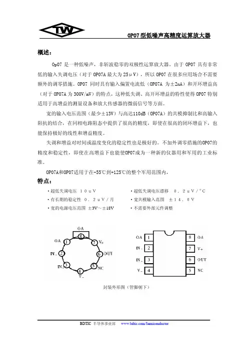
OP07型低噪声高精度运算放大器概述:Op07是一种低噪声,非斩波稳零的双极性运算放大器。
由于OP07具有非常低的输入失调电压(对于OP07A 最大为25μV),所以OP07在很多应用场合不需要额外的调零措施。
OP07同时具有输入偏置电流低(OP07A 为±2nA)和开环增益高(对于OP07A 为300V/mV)的特点,这种低失调、高开环增益的特性使得OP07特别适用于高增益的测量设备和放大传感器的微弱信号等方面。
宽的输入电压范围(最少±13V)与高达110dB(OP07A)的共模抑制比和高输入阻抗的结合,在同相电路阻态中提供了很高的精度,即使在很高的闭环增益下,也能保持极好的线性和增益精度。
失调和增益对时间或温度变化的稳定性也是极好的。
不加外调零措施的OP07的精度和稳定性,即使在高增益下也能使OP07成为一种新的仪器用和军用的工业标准。
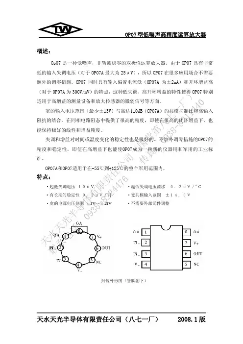
OP07A和OP07适用于在-55℃到+125℃的整个军用范围内,特点:·超低失调电压 10uV ·超低失调电压漂移 0.2uV/OC·有长期的稳定性 0.2uV/月 ·宽共模输入范围 ±14.0V ·宽的电源电压范围 ±3V ~±18V ·不需要外部元件调整封装外形图(管脚朝下)天水天光半导体有限责任公司(国营第八七一厂)联系电话:0938-******* 传真:0938-*******OP07型低噪声高精度运算放大器电路原理图:绝对最大额定值:(TA=25℃)电源电压: …………………………………………..±22V 内部功耗(注1):……………………. ………. 500mW 差模输入电压 :………………………………… …±30 V 输入电压(注3): ………………………………….±22V 输出短路持续时间 :………………………………….不限 工作温度范围(OP07A 、OP07):……. -55℃~+125℃ 储存温度范围:…………………………. -65℃~+150℃ 引线温度范围(焊接,60s ):……………………. 300℃ 注1:见最大环境温度额定值和降低系数表封装形式 额定状态下的最大环境温度 在最大环境温度以上要降低的系数 金属圆壳 80℃ 7.1mW/℃ 陶瓷双列 75℃6.7mW/℃注2:若不另作说明,绝对最大额定值既适用于封装的器件,也适用于芯片。
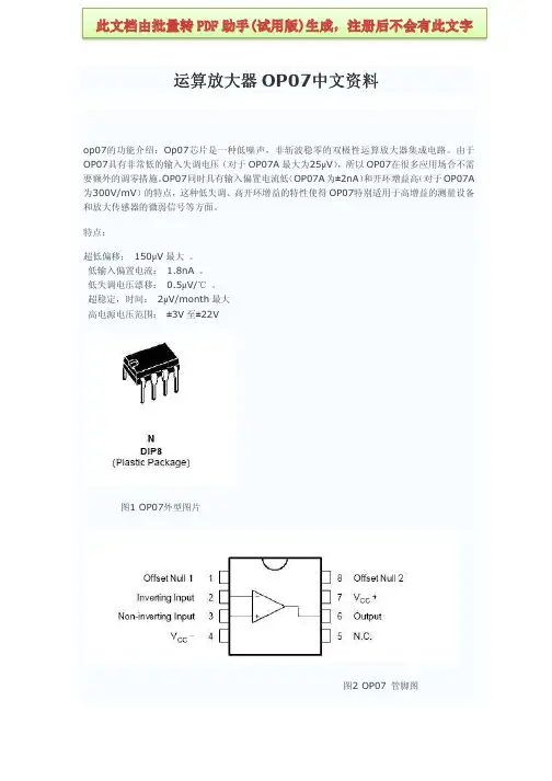
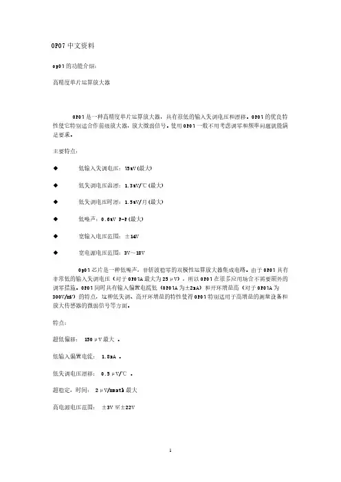
op07中文资料一、引言本文档旨在为读者提供关于OP07运算放大器的中文资料。
OP07是一种高性能精密运算放大器,被广泛应用于工业控制、仪器仪表和传感器信号调理等领域。
本文将介绍OP07的基本特性、电路应用、性能参数等内容,以帮助读者更好地了解和应用OP07。
二、OP07概述OP07是由美国ADI(Analog Devices Inc.)公司推出的一种低噪声、低失调、高增益的运算放大器。
其内部电路采用了差动输入、差动输出的架构,使其具有良好的共模抑制比和噪声性能。
OP07采用超低温漂技术,使其在温度变化较大的环境下依然能提供稳定的性能。
三、OP07特性1. 低噪声OP07的噪声系数非常低,通常在10nV/√Hz以下。
这使得OP07能够处理微弱信号并提供高信噪比的放大功能。
2. 低失调OP07具有低失调和低温漂特性,其失调电压和失调电流均较小。
这使得OP07能够准确放大输入信号,不会引入过多失真。
3. 高增益OP07的开环增益非常高,通常在100dB以上。
高增益使得OP07对输入信号的放大能力更强,可适用于高精度、低噪声的应用场景。
4. 宽电源范围OP07的电源电压范围较宽,通常可以工作在±15V的电源电压下。
这使得OP07适用于不同电源供电的应用场合。
四、OP07应用OP07广泛应用于各种需要高精度、低噪声放大的场合,下面列举了一些常见的应用示例:1. 传感器信号调理OP07可以用于处理传感器输出信号,提供高增益、低噪声的放大功能。
例如,温度传感器、压力传感器、光电传感器等信号的放大和调理。
2. 工业自动化OP07可用于工业控制中的PID控制、测量仪表和反馈控制等场合。
其高精度、低噪声的特性能够提供稳定和精确的控制。
3. 仪器仪表OP07可用于精密仪器仪表中的放大和信号调理,如电压测量仪、电流测量仪、频率计等。
其高性能可以提供准确的测量结果。
4. 数据采集OP07适用于数据采集系统中的信号放大和调理。
op07的功能介绍
op07的功能介绍:
Op07芯片是一种低噪声,非斩波稳零的双极性运算放大器集成电路。
由于OP07具有非常低的输入失调电压(对于OP07A最大为25μV),所以OP07在很多应用场合不需要额外的调零措施。
OP07同时具有输入偏置电流低(OP07A为±2nA)和开环增益高(对于OP07A为300V/mV)的特点,这种低失调、高开环增益的特性使得OP07特别适用于高增益的测量设备和放大传感器的微弱信号等方面。
特点:
超低偏移: 150μV最大。
低输入偏置电流: 1.8nA 。
低失调电压漂移: 0.5μV/℃ 。
超稳定,时间: 2μV/month最大
高电源电压范围:±3V至±22V
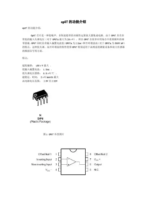
图1 OP07外型图片
图2 OP07 管脚图
OP07芯片引脚功能说明:
1和8为偏置平衡(调零端),2为反向输入端,3为正向输入端,4接地,5空脚 6为输出,7接电源+
图3 OP07内部电路图
ABSOLUTE MAXIMUM RATINGS 最大额定值
电气特性
虚拟通道连接= ± 15V ,Tamb = 25 ℃(除非另有说明)
图4 输入失调电压调零电路
应用电路图:
图5 典型的偏置电压试验电路
图6 老化电路
图7 典型的低频噪声放大电路
图8 高速综合放大器
图9 选择偏移零电路
图10 调整精度放大器
图11 高稳定性的热电偶放大器。

O P07资料OP07中文资料op07的功能介绍:高精度单片运算放大器OP07是一种高精度单片运算放大器,具有很低的输入失调电压和漂移。
OP07的优良特性使它特别适合作前级器,放大微弱信号。
使用OP07一般不用考虑调零和频率问题就能满足要求。
主要特点:◆低输入失调电压:75uV(最大)◆低失调电压温漂:1.3uV/℃(最大)◆低失调电压时漂:1.5uV/月(最大)◆低噪声:0.6uV P-P(最大)◆宽输入电压范围:±14V◆宽电源电压范围:3V~18VOp07芯片是一种低噪声,非斩波稳零的双极性运算放大器集成电路。
由于OP07具有非常低的输入失调电压OP07A最大为25μV),所以OP07在很多应用场合不需要额外的调零措施。
OP07同时具有输入偏置电流低(OP07A为和开环增益高(对于OP07A为300V/mV)的特点,这种低失调、高开环增益的特性使得OP07特别适用于高增益的测量放大传感器的微弱信号等方面。
特点:超低偏移:150μV最大。
低输入偏置电流: 1.8nA 。
低失调电压漂移:0.5μV/℃ 。
超稳定,时间:2μV/month最大高电源电压范围:±3V至±22V图1 OP07外型图片2 OP07 管脚图OP07芯片引脚功能说明:1和8为偏置平衡(调零端),2为反向输入端,3为正向输入端,4接地,5空脚 6为输出,7接电源+图3 OP0路图ABSOLUTE MAXIMUM RATINGS 最大额定值Symbol 符号Parameter参数Value数值Unit单位VCC Supply Voltage 电源电压±22 V Vid Differential Input Voltage差分输入电压±30 V Vi Input Voltage 输入电压±22 V Toper Operating Temperature 工作温度-40 to +105 ℃ Tstg Storage Temperature 贮藏温度-65 to +150 ℃电气特性虚拟通道连接= ± 15V ,Tamb = 25 ℃(除非另有说明)Symbol 符号Parameter 参数及测试条件最小典型最大Unit单位Vio Input Offset Voltage 输入失调电压0℃ ≤ Tamb ≤ +70℃ -60 150250μVLong Term Input Offset Voltage Stability-(note 1) 长期输入偏置电压的稳定性-0.4 2 μV/Mo图4 输入失调电压调零电路应用电路图:图5 典型的偏置电压试验电路图6 老化电路图7 典型的低频噪声放大电路图8 高速综合放大器图9 选择偏移零电路图10 调整精度放大器图11 高稳定性的热电偶放大器图12 精密绝对值电路。
op07cdr中⽂资料OUT+OFFSET N2IN?IN+OFFSET N1132861Features3DescriptionThese devices offer low offset and long-term stability ?Low Noiseby means of a low-noise,chopperless,?No External Components Requiredbipolar-input-transistor amplifier circuit.For most ?Replace Chopper Amplifiers at a Lower Cost applications,external components are not required for offset nulling and frequency compensation.The ? Wide Input-Voltage Range:0to ±14V (Typ)true differential input,with a wide input-voltage range ?Wide Supply-Voltage Range:±3V to ±18Vand outstanding common-mode rejection,provides maximum flexibility and performance in high-noise 2Applicationsenvironments and in noninverting applications.Low bias currents and extremely high input impedances ?Wireless Base Station Control Circuits are maintained over the entire temperature range. Optical Network Control Circuits InstrumentationDevice Information (1)Sensors and Controls PART NUMBER PACKAGE (PIN)BODY SIZEPrecision FiltersSO (8) 6.20mm ×5.30mm OP07xSOIC (8) 4.90mm ×3.91mm PDIP (8)9.81mm ×6.35mm(1)For all available packages,see the orderable addendum atthe end of the data sheet.4Simplified SchematicAn IMPORTANT NOTICE at the end of this data sheet addresses availability,warranty,changes,use in safety-critical applications,intellectual property matters and other important disclaimers.PRODUCTION DATA.找电⼦元器件上宇航军⼯OP07C,OP07DSLOS099G–OCTOBER1983–REVISED NOVEMBER2014Table of Contents9.2Functional Block Diagram (7)1Features (1)9.3Feature Description (7)2Applications (1)9.4Device Functional Modes (7)3Description (1)10Application and Implementation (8)4Simplified Schematic (1)10.1General Application (8)5Revision History (2)10.2Typical Application (8)6Pin Functions (3)11Power Supply Recommendations (10)7Specifications (4)12Layout (11)7.1Absolute Maximum Ratings (4)12.1Layout Guidelines (11)7.2Handling Ratings (4)12.2Layout Example (11)7.3Recommended Operating Conditions (4)13Device and Documentation Support (12)7.4Thermal Information (4)13.1Related Links (12)7.5Electrical Characteristics (5)13.2Trademarks (12)7.6Operating Characteristics (6)13.3Electrostatic Discharge Caution (12)8Typical Characteristics (6)13.4Glossary (12)9Detailed Description (7)14Mechanical,Packaging,and Orderable9.1Overview (7)Information (12)5Revision HistoryChanges from Revision F(January2014)to Revision G Page ?Added Applications,Device Information table,Pin Functions table,Handling Ratings table,Thermal Information table,Typical Characteristics,Feature Description section,Device Functional Modes,Application andImplementation section,Power Supply Recommendations section,Layout section,Device and DocumentationSupport section,and Mechanical,Packaging,and Orderable Information section (1)Changes from Revision E(May2004)to Revision F Page ?Deleted Ordering Information table (1)2Submit Documentation Feedback Copyright?1983–2014,Texas Instruments IncorporatedProduct Folder Links:OP07C OP07D12348765OFFSET N1IN?IN+V CC?OFFSET N2V CC+OUT NCD OR P PACKAGE(TOP VIEW)NC ?No internal connectionOP07C,OP07DSLOS099G –OCTOBER 1983–REVISED NOVEMBER 20146Pin FunctionsPin FunctionsPINTYPE DESCRIPTIONNAME NO.IN+3I Noninverting input IN–2I Inverting input NC5—Do not connectOFFSET N11I External input offset voltage adjustment OFFSET N28I External input offset voltage adjustment OUT 6O Output V CC +7—Positive supply V CC –4—Negative supplyCopyright ?1983–2014,Texas Instruments Incorporated Submit Documentation Feedback3Product Folder Links:OP07C OP07DOP07C,OP07DSLOS099G–OCTOBER1983–REVISED NOVEMBER201411Power Supply RecommendationsThe OP07is specified for operation from±3to±18V;many specifications apply from0°C to70°C.CAUTIONSupply voltages larger than±22V can permanently damage the device(see theAbsolute Maximum Ratings).Place0.1-µF bypass capacitors close to the power-supply pins to reduce errors coupling in from noisy or high impedance power supplies.For more detailed information on bypass capacitor placement,refer to the Layout Guidelines.10Submit Documentation Feedback Copyright?1983–2014,Texas Instruments IncorporatedProduct Folder Links:OP07C OP07D。
OP07中文资料op07的功能介绍:高精度单片运算放大器OP07是一种高精度单片运算放大器,具有很低的输入失调电压和漂移。
OP07的优良特性使它特别适合作前级放大器,放大微弱信号。
使用OP07一般不用考虑调零和频率问题就能满足要求。
主要特点:◆低输入失调电压:75uV(最大)◆低失调电压温漂:1.3uV/℃(最大)◆低失调电压时漂:1.5uV/月(最大)◆低噪声:0.6uV P-P(最大)◆宽输入电压范围:±14V◆宽电源电压范围:3V~18VOp07芯片是一种低噪声,非斩波稳零的双极性运算放大器集成电路。
由于OP07具有非常低的输入失调电压(对于OP07A最大为25μV),所以OP07在很多应用场合不需要额外的调零措施。
OP07同时具有输入偏置电流低(OP07A为±2nA)和开环增益高(对于OP07A为300V/mV)的特点,这种低失调、高开环增益的特性使得OP07特别适用于高增益的测量设备和放大传感器的微弱信号等方面。
特点:超低偏移:150μV最大。
低输入偏置电流: 1.8nA 。
低失调电压漂移:0.5μV/℃ 。
超稳定,时间:2μV/month最大高电源电压范围:±3V至±22V图1 OP07外型图片图2 OP07 管脚图OP07芯片引脚功能说明:1和8为偏置平衡(调零端),2为反向输入端,3为正向输入端,4接地,5空脚 6为输出,7接电源+图3 OP07内部电路图ABSOLUTE MAXIMUM RATINGS 最大额定值Symbol符号Parameter参数Value数值VCC Supply Voltage 电源电压±22Vid Differential Input Voltage差分输入电压±30Vi Input Voltage 输入电压±22Toper Operating Temperature 工作温度-40 to +105 Tstg Storage Temperature 贮藏温度-65 to +150 电气特性虚拟通道连接= ± 15V ,Tamb = 25 ℃(除非另有说明)Symbol符号Parameter 参数及测试条件最小典型最Vio Input Offset Voltage 输入失调电压0℃ ≤ Tamb ≤ +70℃ -60 1525入噪声电压 f = 1kHz-1011.5in Equivalent InputNoise Current 等效输入噪声电流f = 10Hz-0.3 0.9PA√Hzf = 100Hz-0.20.3f = 1kHz-0.1 0.2图4 输入失调电压调零电路应用电路图:图5 典型的偏置电压试验电路图6 老化电路图7 典型的低频噪声放大电路图8 高速综合放大器图9 选择偏移零电路图10 调整精度放大器图11 高稳定性的热电偶放大器图12 精密绝对值电路。