Nanoepitaxy to improve the efficiency of InGaN light-emitting diodes
- 格式:pdf
- 大小:879.96 KB
- 文档页数:4

低功率激光照射诱导的细胞外调节蛋白激酶的激活促进一氧化氮的产生冯杰;吴胜男【摘要】Low-power laser irradiation ( LPLI) , as a non-damage physical therapy, acclerrates cell survival, angiogen-esis and wound healing in which nitric oxide (NO) acts as an important contributor. NO promotes the tendency of inflammation cell, increases the synthesis and precipitation of collagen, and stimulates cell proliferation and angiogenesis. In this study, we found that LPLI boosted the production of NO, which was inhibited by blocking ERK ( Extracellular signal-regulated protein kinase, ERK) activation, indicating LPLI promoted NO generation through activating ERK. The research will supply potential strategy for the clinical application of LPLI in the treatment of wound healing.%低功率激光(632.8 nm)照射(Low-power laser irradiation,LPLI)生物组织作为一种无损伤的物理疗法,可以加速细胞生长、血管再生及伤口愈合等过程.一氧化氮( Nitric oxide,NO)是伤口愈合的关键因素之一,其促进炎性细胞的趋化,增强胶原的合成和沉积,刺激细胞增殖和新生血管生成.我们研究发现LPLI可以促进NO的产生,并且抑制细胞外调节蛋白激酶(Extracellular signal-regulated protein kinases,ERK)的活性阻碍了NO的产生,证明LPLI通过活化ERK调控NO的生成.这一研究将为低功率激光照射加速伤口愈合在临床上的应用奠定基础.【期刊名称】《激光生物学报》【年(卷),期】2012(021)004【总页数】5页(P299-303)【关键词】低功率激光照射;伤口愈合;一氧化氮;细胞外调节蛋白激酶【作者】冯杰;吴胜男【作者单位】华南师范大学生物光子学研究院激光生命科学研究所,暨激光生命科学教育部重点实验室,广东广州510631;华南师范大学生物光子学研究院激光生命科学研究所,暨激光生命科学教育部重点实验室,广东广州510631【正文语种】中文【中图分类】Q631低功率激光(632.8 nm)照射(low-power laser irradiation,LPLI)生物组织时,激光能量没有达到破坏的程度,热效应和压强效应不占主导地位,主要是通过光的生物调节和生物刺激效应,促进细胞的生存、增殖和分化[1,2],加速血液循环、促进细胞生长和组织修复,使得LPLI在许多疾病的治疗中受到越来越多的关注,如中风、炎症、血管再生和伤口愈合[3-5]。

Semiconductor Manufacturing Technology半导体制造技术Instructor’s ManualMichael QuirkJulian SerdaCopyright Prentice HallTable of Contents目录OverviewI. Chapter1. Semiconductor industry overview2. Semiconductor materials3. Device technologies—IC families4. Silicon and wafer preparation5. Chemicals in the industry6. Contamination control7. Process metrology8. Process gas controls9. IC fabrication overview10. Oxidation11. Deposition12. Metallization13. Photoresist14. Exposure15. Develop16. Etch17. Ion implant18. Polish19. Test20. Assembly and packagingII. Answers to End-of-Chapter Review QuestionsIII. Test Bank (supplied on diskette)IV. Chapter illustrations, tables, bulleted lists and major topics (supplied on CD-ROM)Notes to Instructors:1)The chapter overview provides a concise summary of the main topics in each chapter.2)The correct answer for each test bank question is highlighted in bold. Test bankquestions are based on the end-of-chapter questions. If a student studies the end-of-chapter questions (which are linked to the italicized words in each chapter), then they will be successful on the test bank questions.2Chapter 1Introduction to the Semiconductor Industry Die:管芯 defective:有缺陷的Development of an Industry•The roots of the electronic industry are based on the vacuum tube and early use of silicon for signal transmission prior to World War II. The first electronic computer, the ENIAC, wasdeveloped at the University of Pennsylvania during World War II.•William Shockley, John Bardeen and Walter Brattain invented the solid-state transistor at Bell Telephone Laboratories on December 16, 1947. The semiconductor industry grew rapidly in the 1950s to commercialize the new transistor technology, with many early pioneers working inSilicon Valley in Northern California.Circuit Integration•The first integrated circuit, or IC, was independently co-invented by Jack Kilby at Texas Instruments and Robert Noyce at Fairchild Semiconductor in 1959. An IC integrates multiple electronic components on one substrate of silicon.•Circuit integration eras are: small scale integration (SSI) with 2 - 50 components, medium scale integration (MSI) with 50 – 5k components, large scale integration (LSI) with 5k to 100kcomponents, very large scale integration (VLSI) with 100k to 1M components, and ultra large scale integration (ULSI) with > 1M components.1IC Fabrication•Chips (or die) are fabricated on a thin slice of silicon, known as a wafer (or substrate). Wafers are fabricated in a facility known as a wafer fab, or simply fab.•The five stages of IC fabrication are:Wafer preparation: silicon is purified and prepared into wafers.Wafer fabrication: microchips are fabricated in a wafer fab by either a merchant chip supplier, captive chip producer, fabless company or foundry.Wafer test: Each individual die is probed and electrically tested to sort for good or bad chips.Assembly and packaging: Each individual die is assembled into its electronic package.Final test: Each packaged IC undergoes final electrical test.•Key semiconductor trends are:Increase in chip performance through reduced critical dimensions (CD), more components per chip (Moore’s law, which predicts the doubling of components every 18-24 months) andreduced power consumption.Increase in chip reliability during usage.Reduction in chip price, with an estimated price reduction of 100 million times for the 50 years prior to 1996.The Electronic Era•The 1950s saw the development of many different types of transistor technology, and lead to the development of the silicon age.•The 1960s were an era of process development to begin the integration of ICs, with many new chip-manufacturing companies.•The 1970s were the era of medium-scale integration and saw increased competition in the industry, the development of the microprocessor and the development of equipment technology. •The 1980s introduced automation into the wafer fab and improvements in manufacturing efficiency and product quality.•The 1990s were the ULSI integration era with the volume production of a wide range of ICs with sub-micron geometries.Career paths•There are a wide range of career paths in semiconductor manufacturing, including technician, engineer and management.2Chapter 2 Characteristics of Semiconductor MaterialsAtomic Structure•The atomic model has three types of particles: neutral neutrons(不带电的中子), positively charged protons(带正电的质子)in the nucleus and negatively charged electrons(带负电的核外电子) that orbit the nucleus. Outermost electrons are in the valence shell, and influence the chemical and physical properties of the atom. Ions form when an atom gains or loses one or more electrons.The Periodic Table•The periodic table lists all known elements. The group number of the periodic table represents the number of valence shell electrons of the element. We are primarily concerned with group numbers IA through VIIIA.•Ionic bonds are formed when valence shell electrons are transferred from the atoms of one element to another. Unstable atoms (e.g., group VIIIA atoms because they lack one electron) easily form ionic bonds.•Covalent bonds have atoms of different elements that share valence shell electrons.3Classifying Materials•There are three difference classes of materials:ConductorsInsulatorsSemiconductors•Conductor materials have low resistance to current flow, such as copper. Insulators have high resistance to current flow. Capacitance is the storage of electrical charge on two conductive plates separated by a dielectric material. The quality of the insulation material between the plates is the dielectric constant. Semiconductor materials can function as either a conductor or insulator.Silicon•Silicon is an elemental semiconductor material because of four valence shell electrons. It occurs in nature as silica and is refined and purified to make wafers.•Pure silicon is intrinsic silicon. The silicon atoms bond together in covalent bonds, which defines many of silicon’s properties. Silicon atoms bond together in set, repeatable patterns, referred to asa crystal.•Germanium was the first semiconductor material used to make chips, but it was soon replaced by silicon. The reasons for this change are:Abundance of siliconHigher melting temperature for wider processing rangeWide temperature range during semiconductor usageNatural growth of silicon dioxide•Silicon dioxide (SiO2) is a high quality, stable electrical insulator material that also serves as a good chemical barrier to protect silicon from external contaminants. The ability to grow stable, thin SiO2 is fundamental to the fabrication of Metal-Oxide-Semiconductor (MOS) devices. •Doping increases silicon conductivity by adding small amounts of other elements. Common dopant elements are from trivalent, p-type Group IIIA (boron) and pentavalent, n-type Group VA (phosphorus, arsenic and antimony).•It is the junction between the n-type and p-type doped regions (referred to as a pn junction) that permit silicon to function as a semiconductor.4Alternative Semiconductor Materials•The alternative semiconductor materials are primarily the compound semiconductors. They are formed from Group IIIA and Group VA (referred to as III-V compounds). An example is gallium arsenide (GaAs).•Some alternative semiconductors come from Group IIA and VIA, referred to as II-VI compounds. •GaAs is the most common III-V compound semiconductor material. GaAs ICs have greater electron mobility, and therefore are faster than ICs made with silicon. GaAs ICs also have higher radiation hardness than silicon, which is better for space and military applications. The primary disadvantage of GaAs is the lack of a natural oxide.5Chapter 3Device TechnologiesCircuit Types•There are two basic types of circuits: analog and digital. Analog circuits have electrical data that varies continuously over a range of voltage, current and power values. Digital circuits have operating signals that vary about two distinct voltage levels – a high and a low.Passive Component Structures•Passive components such as resistors and capacitors conduct electrical current regardless of how the component is connected. IC resistors are a passive component. They can have unwanted resistance known as parasitic resistance. IC capacitor structures can also have unintentional capacitanceActive Component Structures•Active components, such as diodes and transistors can be used to control the direction of current flow. PN junction diodes are formed when there is a region of n-type semiconductor adjacent to a region of p-type semiconductor. A difference in charge at the pn junction creates a depletion region that results in a barrier voltage that must be overcome before a diode can be operated. A bias voltage can be configured to have a reverse bias, with little or no conduction through the diode, or with a forward bias, which permits current flow.•The bipolar junction transistor (BJT) has three electrodes and two pn junctions. A BJT is configured as an npn or pnp transistor and biased for conduction mode. It is a current-amplifying device.6• A schottky diode is formed when metal is brought in contact with a lightly doped n-type semiconductor material. This diode is used in faster and more power efficient BJT circuits.•The field-effect transistor (FET), a voltage-amplifying device, is more compact and power efficient than BJT devices. A thin gate oxide located between the other two electrodes of the transistor insulates the gate on the MOSFET. There are two categories of MOSFETs, nMOS (n-channel) and pMOS (p-channel), each which is defined by its majority current carriers. There is a biasing scheme for operating each type of MOSFET in conduction mode.•For many years, nMOS transistors have been the choice of most IC manufacturers. CMOS, with both nMOS and pMOS transistors in the same IC, has been the most popular device technology since the early 1980s.•BiCMOS technology makes use of the best features of both CMOS and bipolar technology in the same IC device.•Another way to categorize FETs is in terms of enhancement mode and depletion mode. The major different is in the way the channels are doped: enhancement-mode channels are doped opposite in polarity to the source and drain regions, whereas depletion mode channels are doped the same as their respective source and drain regions.Latchup in CMOS Devices•Parasitic transistors can create a latchup condition(???????) in CMOS ICs that causes transistors to unintentionally(无心的) turn on. To control latchup, an epitaxial layer is grown on the wafer surface and an isolation barrier(隔离阻障)is placed between the transistors. An isolation layer can also be buried deep below the transistors.Integrated Circuit Productsz There are a wide range of semiconductor ICs found in electrical and electronic products. This includes the linear IC family, which operates primarily with anal3og circuit applications, and the digital IC family, which includes devices that operate with binary bits of data signals.7Chapter 4Silicon and Wafer Preparation8z Semiconductor-Grade Silicon•The highly refined silicon used for wafer fabrication is termed semiconductor-grade silicon (SGS), and sometimes referred to as electronic-grade silicon. The ultra-high purity of semiconductor-grade silicon is obtained from a multi-step process referred to as the Siemens process.Crystal Structure• A crystal is a solid material with an ordered, 3-dimensional pattern over a long range. This is different from an amorphous material that lacks a repetitive structure.•The unit cell is the most fundamental entity for the long-range order found in crystals. The silicon unit cell is a face-centered cubic diamond structure. Unit cells can be organized in a non-regular arrangement, known as a polycrystal. A monocrystal are neatly arranged unit cells.Crystal Orientation•The orientation of unit cells in a crystal is described by a set of numbers known as Miller indices.The most common crystal planes on a wafer are (100), (110), and (111). Wafers with a (100) crystal plane orientation are most common for MOS devices, whereas (111) is most common for bipolar devices.Monocrystal Silicon Growth•Silicon monocrystal ingots are grown with the Czochralski (CZ) method to achieve the correct crystal orientation and doping. A CZ crystal puller is used to grow the silicon ingots. Chunks of silicon are heated in a crucible in the furnace of the puller, while a perfect silicon crystal seed is used to start the new crystal structure.• A pull process serves to precisely replicate the seed structure. The main parameters during the ingot growth are pull rate and crystal rotation. More homogeneous crystals are achieved with a magnetic field around the silicon melt, known as magnetic CZ.•Dopant material is added to the melt to dope the silicon ingot to the desired electrical resistivity.Impurities are controlled during ingot growth. A float-zone crystal growth method is used toachieve high-purity silicon with lower oxygen content.•Large-diameter ingots are grown today, with a transition underway to produce 300-mm ingot diameters. There are cost benefits for larger diameter wafers, including more die produced on a single wafer.Crystal Defects in Silicon•Crystal defects are interruptions in the repetitive nature of the unit cell. Defect density is the number of defects per square centimeter of wafer surface.•Three general types of crystal defects are: 1) point defects, 2) dislocations, and 3) gross defects.Point defects are vacancies (or voids), interstitial (an atom located in a void) and Frenkel defects, where an atom leaves its lattice site and positions itself in a void. A form of dislocation is astacking fault, which is due to layer stacking errors. Oxygen-induced stacking faults are induced following thermal oxidation. Gross defects are related to the crystal structure (often occurring during crystal growth).Wafer Preparation•The cylindrical, single-crystal ingot undergoes a series of process steps to create wafers, including machining operations, chemical operations, surface polishing and quality checks.•The first wafer preparation steps are the shaping operations: end removal, diameter grinding, and wafer flat or notch. Once these are complete, the ingot undergoes wafer slicing, followed by wafer lapping to remove mechanical damage and an edge contour. Wafer etching is done to chemically remove damage and contamination, followed by polishing. The final steps are cleaning, wafer evaluation and packaging.Quality Measures•Wafer suppliers must produce wafers to stringent quality requirements, including: Physical dimensions: actual dimensions of the wafer (e.g., thickness, etc.).Flatness: linear thickness variation across the wafer.Microroughness: peaks and valleys found on the wafer surface.Oxygen content: excessive oxygen can affect mechanical and electrical properties.Crystal defects: must be minimized for optimum wafer quality.Particles: controlled to minimize yield loss during wafer fabrication.Bulk resistivity(电阻系数): uniform resistivity from doping during crystal growth is critical. Epitaxial Layer•An epitaxial layer (or epi layer) is grown on the wafer surface to achieve the same single crystal structure of the wafer with control over doping type of the epi layer. Epitaxy minimizes latch-up problems as device geometries continue to shrink.Chapter 5Chemicals in Semiconductor FabricationEquipment Service Chase Production BayChemical Supply Room Chemical Distribution Center Holding tank Chemical drumsProcess equipmentControl unit Pump Filter Raised and perforated floorElectronic control cablesSupply air ductDual-wall piping for leak confinement PumpFilterChemical control and leak detection Valve boxes for leak containment Exhaust air ductStates of Matter• Matter in the universe exists in 3 basic states (宇宙万物存在着三种基本形态): solid, liquid andgas. A fourth state is plasma.Properties of Materials• Material properties are the physical and chemical characteristics that describe its unique identity.• Different properties for chemicals in semiconductor manufacturing are: temperature, pressure andvacuum, condensation, vapor pressure, sublimation and deposition, density, surface tension, thermal expansion and stress.Temperature is a measure of how hot or cold a substance is relative to another substance. Pressure is the force exerted per unit area. Vacuum is the removal of gas molecules.Condensation is the process of changing a gas into a liquid. Vaporization is changing a liquidinto a gas.Vapor pressure is the pressure exerted by a vapor in a closed container at equilibrium.Sublimation is the process of changing a solid directly into a gas. Deposition is changing a gas into a solid.Density is the mass of a substance divided by its volume.Surface tension of a liquid is the energy required to increase the surface area of contact.Thermal expansion is the increase in an object’s dimension due to heating.Stress occurs when an object is exposed to a force.Process Chemicals•Semiconductor manufacturing requires extensive chemicals.• A chemical solution is a chemical mixture. The solvent is the component of the solution present in larger amount. The dissolved substances are the solutes.•Acids are solutions that contain hydrogen and dissociate in water to yield hydronium ions. A base is a substance that contains the OH chemical group and dissociates in water to yield the hydroxide ion, OH-.•The pH scale is used to assess the strength of a solution as an acid or base. The pH scale varies from 0 to 14, with 7 being the neutral point. Acids have pH below 7 and bases have pH values above 7.• A solvent is a substance capable of dissolving another substance to form a solution.• A bulk chemical distribution (BCD) system is often used to deliver liquid chemicals to the process tools. Some chemicals are not suitable for BCD and instead use point-of-use (POU) delivery, which means they are stored and used at the process station.•Gases are generally categorized as bulk gases or specialty gases. Bulk gases are the relatively simple gases to manufacture and are traditionally oxygen, nitrogen, hydrogen, helium and argon.The specialty gases, or process gases, are other important gases used in a wafer fab, and usually supplied in low volume.•Specialty gases are usually transported to the fab in metal cylinders.•The local gas distribution system requires a gas purge to flush out undesirable residual gas. Gas delivery systems have special piping and connections systems. A gas stick controls the incoming gas at the process tool.•Specialty gases may be classified as hydrides, fluorinated compounds or acid gases.Chapter 6Contamination Control in Wafer FabsIntroduction•Modern semiconductor manufacturing is performed in a cleanroom, isolated from the outside environment and contaminants.Types of contamination•Cleanroom contamination has five categories: particles, metallic impurities, organic contamination, native oxides and electrostatic discharge. Killer defects are those causes of failure where the chip fails during electrical test.Particles: objects that adhere to a wafer surface and cause yield loss. A particle is a killer defect if it is greater than one-half the minimum device feature size.Metallic impurities: the alkali metals found in common chemicals. Metallic ions are highly mobile and referred to as mobile ionic contaminants (MICs).Organic contamination: contains carbon, such as lubricants and bacteria.Native oxides: thin layer of oxide growth on the wafer surface due to exposure to air.Electrostatic discharge (ESD): uncontrolled transfer of static charge that can damage the microchip.Sources and Control of Contamination•The sources of contamination in a wafer fab are: air, humans, facility, water, process chemicals, process gases and production equipment.Air: class number designates the air quality inside a cleanroom by defining the particle size and density.Humans: a human is a particle generator. Humans wear a cleanroom garment and follow cleanroom protocol to minimize contamination.Facility: the layout is generally done as a ballroom (open space) or bay and chase design.Laminar airflow with air filtering is used to minimize particles. Electrostatic discharge iscontrolled by static-dissipative materials, grounding and air ionization.Ultrapure deiniozed (DI) water: Unacceptable contaminants are removed from DI water through filtration to maintain a resistivity of 18 megohm-cm. The zeta potential represents a charge on fine particles in water, which are trapped by a special filter. UV lamps are used for bacterial sterilization.Process chemicals: filtered to be free of contamination, either by particle filtration, microfiltration (membrane filter), ultrafiltration and reverse osmosis (or hyperfiltration).Process gases: filtered to achieve ultraclean gas.Production equipment: a significant source of particles in a fab.Workstation design: a common layout is bulkhead equipment, where the major equipment is located behind the production bay in the service chase. Wafer handling is done with robotic wafer handlers. A minienvironment is a localized environment where wafers are transferred on a pod and isolated from contamination.Wafer Wet Cleaning•The predominant wafer surface cleaning process is with wet chemistry. The industry standard wet-clean process is the RCA clean, consisting of standard clean 1 (SC-1) and standard clean 2 (SC-2).•SC-1 is a mixture of ammonium hydroxide, hydrogen peroxide and DI water and capable of removing particles and organic materials. For particles, removal is primarily through oxidation of the particle or electric repulsion.•SC-2 is a mixture of hydrochloric acid, hydrogen peroxide and DI water and used to remove metals from the wafer surface.•RCA clean has been modified with diluted cleaning chemistries. The piranha cleaning mixture combines sulfuric acid and hydrogen peroxide to remove organic and metallic impurities. Many cleaning steps include an HF last step to remove native oxide.•Megasonics(兆声清洗) is widely used for wet cleaning. It has ultrasonic energy with frequencies near 1 MHz. Spray cleaning will spray wet-cleaning chemicals onto the wafer. Scrubbing is an effective method for removing particles from the wafer surface.•Wafer rinse is done with overflow rinse, dump rinse and spray rinse. Wafer drying is done with spin dryer or IPA(异丙醇) vapor dry (isopropyl alcohol).•Some alternatives to RCA clean are dry cleaning, such as with plasma-based cleaning, ozone and cryogenic aerosol cleaning.Chapter 7Metrology and Defect InspectionIC Metrology•In a wafer fab, metrology refers to the techniques and procedures for determining physical and electrical properties of the wafer.•In-process data has traditionally been collected on monitor wafers. Measurement equipment is either stand-alone or integrated.•Yield is the percent of good parts produced out of the total group of parts started. It is an indicator of the health of the fabrication process.Quality Measures•Semiconductor quality measures define the requirements for specific aspects of wafer fabrication to ensure acceptable device performance.•Film thickness is generally divided into the measurement of opaque film or transparent film. Sheet resistance measured with a four-point probe is a common method of measuring opaque films (e.g., metal film). A contour map shows sheet resistance deviations across the wafer surface.•Ellipsometry is a nondestructive, noncontact measurement technique for transparent films. It works based on linearly polarized light that reflects off the sample and is elliptically polarized.•Reflectometry is used to measure a film thickness based on how light reflects off the top and bottom surface of the film layer. X-ray and photoacoustic technology are also used to measure film thickness.•Film stress is measured by analyzing changes in the radius of curvature of the wafer. Variations in the refractive index are used to highlight contamination in the film.•Dopant concentration is traditionally measured with a four-point probe. The latest technology is the thermal-wave system, which measures the lattice damage in the implanted wafer after ion implantation. Another method for measuring dopant concentration is spreading resistance probe. •Brightfield detection is the traditional light source for microscope equipment. An optical microscope uses light reflection to detect surface defects. Darkfield detection examines light scattered off defects on the wafer surface. Light scattering uses darkfield detection to detectsurface particles by illuminating the surface with laser light and then using optical imaging.•Critical dimensions (CDs) are measured to achieve precise control over feature size dimensions.The scanning electron microscope is often used to measure CDs.•Conformal step coverage is measured with a surface profiler that has a stylus tip.•Overlay registration measures the ability to accurately print photoresist patterns over a previously etched pattern.•Capacitance-voltage (C-V) test is used to verify acceptable charge conditions and cleanliness at the gate structure in a MOS device.Analytical Equipment•The secondary-ion mass spectrometry (SIMS) is a method of eroding a wafer surface with accelerated ions in a magnetic field to analyze the surface material composition.•The atomic force microscope (AFM) is a surface profiler that scans a small, counterbalanced tip probe over the wafer to create a 3-D surface map.•Auger electron spectroscopy (AES) measures composition on the wafer surface by measuring the energy of the auger electrons. It identifies elements to a depth of about 2 nm. Another instrument used to identify surface chemical species is X-ray photoelectron spectroscopy (XPS).•Transmission electron microscopy (TEM) uses a beam of electrons that is transmitted through a thin slice of the wafer. It is capable of quantifying very small features on a wafer, such as silicon crystal point defects.•Energy-dispersive spectrometer (EDX) is a widely used X-ray detection method for identifying elements. It is often used in conjunction with the SEM.• A focused ion beam (FIB) system is a destructive technique that focuses a beam of ions on the wafer to carve a thin cross section from any wafer area. This permits analysis of the wafermaterial.Chapter 8Gas Control in Process ChambersEtch process chambers••The process chamber is a controlled vacuum environment where intended chemical reactions take place under controlled conditions. Process chambers are often configured as a cluster tool. Vacuum•Vacuum ranges are low (rough) vacuum, medium vacuum, high vacuum and ultrahigh vacuum (UHV). When pressure is lowered in a vacuum, the mean free path(平均自由行程) increases, which is important for how gases flow through the system and for creating a plasma.Vacuum Pumps•Roughing pumps are used to achieve a low to medium vacuum and to exhaust a high vacuum pump. High vacuum pumps achieve a high to ultrahigh vacuum.•Roughing pumps are dry mechanical pumps or a blower pump (also referred to as a booster). Two common high vacuum pumps are a turbomolecular (turbo) pump and cryopump. The turbo pump is a reliable, clean pump that works on the principle of mechanical compression. The cryopump isa capture pump that removes gases from the process chamber by freezing them.。

(要求翻译与毕业设计(论文)相关的外文文献两篇,且3000单词以上/ 篇,将译文附在原文之后)第一篇:[ 所译外文资料:①作者:Taeil Jung②书名(或论文题目):Nano-structured InGaN Light-Emitting Diodesfor Solid-State Lighting③出版社(或刊物名称或可获得地址):All Rights Reserved.④出版时间(或卷期号):2009.⑤所译起止页码:Nano-structured InGaN Light-Emitting Diodesfor Solid-State LightingSolid-state lighting can potentially reduce the electricity consumption by 25%. It requires high efficiency light-emitting diodes across the visible spectrum. GaN and related materials have direct band gap across the entire visible spectrum and are ideal for future solid-state lighting applications. However, materials defects, polarization charges, and total internal reflection have thus far limited the efficiencies of InGaN LEDs, in particular InGaN LEDs in the green/yellow wavelength range, which are critical in achieving highly efficient LED luminaries with an excellent color-rendering indexIn this Thesis, we have developed and demonstrated that novel in situ nanostructured GaN processes in MOCVD are effective in improving the efficiencies of InGaN LEDs. InGaN LEDs grown on quasi-planar semi-polar GaN templates were proven to exhibit three times higher internal quantum efficiencies and negligible quantum confined Stark effect using selective area epitaxy. InGaN LEDs grown on nanostructured semi-polar GaN templates are also effective to improve the internal quantum efficiency by 31%. The same in situ processes are also effective in reducing the defect density by an order of magnitude and increasing the photon extraction efficiency as a factor of two.The in situ processes include in situ silane treatment and high temperature overgrowth. Both processes require only standard MOCVD tools and hence are cost effective and suitable for mass-production. In situ silane treatment treatsc-plane GaN samples with silane under ammonia environment, generating nano-scale truncated cone structures with up to 200 nm scale. These truncated cone structures can be subsequently transformed into pyramidal nanostructures comprising of only (10-11) and (11-22) semipolar planes using high temperature overgrowth. These processes were applied to both InGaN active region and the LED surface to improve the internal quantum efficiency and the photon extraction efficiency, respectively. Extensive materials, device, and optical characterizations have been carried out in this research.1.1 Gallium Nitride Materials for Optoelectronic ApplicationsGallium nitride based materials, including GaN, AlN, InN, and their alloys, are excellent candidates for short-wavelength optoelectronic applications. Their direct bandgaps extend from ultraviolet to near-infrared. In addition, they exhibit high mechanical and thermal stabilities compared to other III-Vsemi-conductors, making them especially suitable for high-power andhigh-temperature operations. In recent years, breakthroughs in p-type doping and defect reduction have led to the commercialization of GaN based laser diodes, light-emitting diodes (LEDs), high electron mobility transistors (HEMT) and hydrogen detectors. Despite these advances, many technological challenges such as green gap and substrate growths still remain.Perhaps one of the most important applications for GaN based materials is solidstate lighting (SSL). Worldwide, lighting constitutes 20% of electricity consumption while its efficiency is much lower than 25%. In contrast, efficiency of space heating has exceeded 90%. To this end, the development of highly efficient and reliable LEDs for solid-state lighting has been very active in both industry and academia in the past few years. It is projected by the US Department of Energy that by 2015, if successful, solidstate lighting can reduce the overall electricity consumption by 25%.Unlike GaAs and InP based semi-conductors, GaN based materials have suffered from a high density of defects due to very limited availability of lattice-matched GaN substrates. Up to now, most GaN based optoelectronic devices have been fabricated using hetero-epitaxy on foreign substrates such as sapphire (Al2O3), silicon carbide (SiC), and aluminum nitride (AlN), and in a very small percentage on silicon. Because of large lattice mismatch, GaN grown on these substrates often exhibits a high density of threading dislocations, typically on the order of 108 – 1010 /cm2. These defects are still one of the major limiting factors for the performance of GaN based optoelectronic devices, acting as non-radiative recombination and scattering centers. Achievement of lower defect density would also improve device reliability, resulting in a longer lifetime. Various defect reduction approaches, such as epitaxial lateral over-growth (ELOG), have been demonstrated and some of the details will be discussed in Chap.1.3.1. As part of this thesis, we have explored a novel approach to using nano-structured GaN to effectively lower the threading dislocation density.Among various epitaxial techniques that have been developed for GaN based materials, metal-organic chemical vapor deposition (MOCVD) is the leading technology. The typical growth temperature for GaN materials is around 1000 to 1200°C. This high growth temperature is necessary to improve the crystal quality and is a result of low cracking efficiency of the nitrogen source, ammonia (NH3), at a low temperature. In Chapter 2, I will summarize my contributions to successfully ramp up an MOCVD tool for the epitaxial growth of GaN LEDs for this research.1.2 InGaN LEDs for Solid-State LightingThe basic component for SSL is a white-light LED. As shown in Figure 1-1, itcan be achieved by mixing various color components, which can be generated either from the direct output of individual LEDs or from color-conversion materials, such as phosphor. To date, commercially available white-light LEDs usually consist of a blue emitter and a yellow phosphor plate. It has been shown that InGaN based blue LEDs could achieve external quantum efficiency in excess of 70% [1, 2]. However, this di-chromatic configuration typically has a poor color rendering index due to the lack of green and red components. The phosphor conversion process also limits the overall luminous efficiency due to energy loss during downconversion. To achieve luminous efficiency in excess of 200 lm/W and a color rendering index (CRI) in excess of 90, which is required for general illumination, a further improvement in blue LED efficiency and the use of tetra-chromatic configuration (blue + green + yellow + red) is necessary [3].* Unfortunately, the efficiency of both InGaN and AlInGaP LEDs decreases significantly in the green-yellow (500 - 580 nm) range. This efficiency gap is also known as “green gap”. Because AlInGaP materials have indirect bandgaps in this wavelength range, to achieve high-efficiency SSL, it is crucial to significantly improve the luminousNote that a trichromatic (e.g. blue + green + red) source cannot achieve a CRI > 90. efficiency of green and yellow InGaN LEDs. In this thesis, we will address these challenges using nano-structured GaN.Figure 1-1. Illustration of various potential white-light LEDs configurations (after Ref. [4]).1.3Limiting Factors for InGaN LEDs EfficiencyTo date, the efficiencies of InGaN LEDs are still limited by materials defects, polarization charges, and photon trapping. In this Section, we will briefly review the state of theart and overview how this research helps address these limitations.1.3.1 Materials DefectsAs mentioned before, the high defect density in GaN based materials grown on foreignsubstrates increases the non-radiative recombination rate and lowers the radiative efficiency. To date, several techniques have been demonstrated to improve the crystal quality and reduce the threading dislocation (TD) density of the GaN layer. Substrate pretreatmentat the growth temperature in an ammonia environment, also known as nitridation [5-7], has been shown to be critical for high quality GaN epilayers. The TD density of a typical GaN layer grown on c-plane sapphire substrate can be reduced to 108/cm2 [8] by employing the combination of a low temperature (LT; 450 - 600 °C)nucleation layer (NL) and a short annealing at the growth temperature to change the phase of the as-grown NL from cubic to hexagonal [9-11]. As will be discussed in Chapter 2, careful optimization of these low temperature growth sequences can significantly alter the subsequent GaN template growth. To this end, a home-made optical in situ monitoring tool (reflectometry) was established and will be discussed extensively in Chapter 2.In addition low temperature buffer growth, epitaxial lateral overgrowth (ELOG) which is a variation of selective area epitaxy (SAE) has been introduced [12, 13] to further lower the TD density by an order of magnitude to below 107/cm2. Variations of ELOG including pendeo- (from the Latin : hang on or suspended from) epitaxy (PE) [14] and multi-step ELOG are also effective to further reduce the TD density. Additional techniques such as TiN nano-porous network [15] and anodic aluminum oxide nano-mask [16] have also been proposed and demonstrated. All these methods, however, require ex situ processing and hence will add complexity and cost to the manufacturing. In this thesis, we will explore and generalize an in situ silane treatment approach to effectively lowering the TD density by an order of magnitude.1.3.2 Polarization ChargesDue to the non-cubic symmetry of GaN materials, compressively-strained active regions in InGaN LEDs exhibit both spontaneous and piezoelectric polarization charges. These polarization charges induce a strong internal electric field (IEF), typically on the order of MV/cm, in the active region, resulting in both efficiency droop at a high injection current density and the decrease of radiative efficiency with an increasing emission wavelength. The IEF can separate electrons from holes and increase electron leakage, resulting in low internal quantum efficiency (IQE) and efficiency droop [17], respectively. The suppression of the IEF, which is expected to increase IQE and the current density at which efficiency droop occurs, can be achieved by reducing the lattice mismatch in hetero-structures or growing them on semi-polar (e.g. {10-11} and {11-22}) and non-polar (e.g. a-plane and m-plane) surfaces. Because indium incorporation is more difficult on non-polar planes than on semi-polar planes, it is more advantageous to fabricate long-wavelength green-yellow LEDs on semi-polar planes to suppress the IEF.At least three approaches to fabricating semi-polar InGaN LEDs have been reported thus far. These include the growth of a GaN epilayer on spinel substrates [18], on bulk GaN substrates [19-27], and on the sidewalls of pyramidal or ridge GaN structures created on planar polar GaN surfaces using SAE [28-35]. GaN grown on spinel substrates have so far exhibited a high density of threading dislocations and stacking faults, thereby compromising the potential improvement of efficiency from the lowering of IEF. The use of bulk semi-polar GaN substrates has demonstrated the advantage of a lower IEF for the enhanced efficiency of green and yellow LEDs [25, 26]. However, limitations such as prohibitively high wafer cost and small substrate size need to be resolved before this approach can become more practical. On the other hand, the SAE technique can create semi-polar planes on polar GaN surfaces.High quality polar GaN films have been fabricated from a variety of substrates including sapphire, 6H-SiC, and bulk GaN by MOCVD. Using growth rate anisotropy and three-dimensional growth, different semi-polar and non-polar GaN planes can be generated on c-plane GaN [13]. In Chapter 3, we will show that high quality InGaN multiple quantum wells (MQWs) which exhibit IQE as large as a factor of three compared to polar MQWs can be grown on pyramidal GaN microstructures. This approach, however, requires ex situ patterning processes and does not easily produce a planar structure for electrical contacts. In this thesis, a new semi-polar LED structure is investigated, which is enabled by a novel epitaxial nanostructure, namely the nanostructured semi-polar (NSSP) GaN, which can be fabricated directly on c-plane GaN but without the issues of the SAE technique mentioned above [36]. NSSP GaN also eliminates the issues of excessive defects for GaN grown on spinel substrates and lowers the cost of using bulk semi-polar GaN substrates. As we will show later, the surface of NSSP GaN consists of two different semi-polar planes: (10-11) and (11-22). Therefore it is expected that InGaN active regions fabricated on NSSP GaN can exhibit a low IEF, and hence much improved IQE.1.3.3 Photon ExtractionAfter photons are generated from the active region in LEDs, they need to escape the device in order to be useful. When light travels from a medium with a higher refractive index to a medium with a lower refractive index, total internal reflection (TIR) occurs at the interface. In InGaN LEDs, photons experiencing TIR at LED surfaces can be re-absorbed by the active region or trapped in the device due to a wave-guiding effect as shown in Figure 1-2. In a simple InGaN LED, only 4% of photons generated from the active region can escape from each device surface. It has been shown that surface textures on LED surfaces can greatly reduce TIR and improve photon extraction efficiency as illustrated in Figure 1-2. To date, many surface texturing techniques such as photonic crystal structures [37] and photo-electrochemical etching of GaN surfaces [38] have been introduced. Notably, the photo-electrochemical etching of nitrogen-terminated GaN surface has been successfully implemented into commercial blue LEDs [2]. However, these approaches all require additional ex situ patterning processes which add significant costs.In this thesis, we investigate an in situ process to fabricate nano-structured GaN surfaces on LEDs which effectively improves the photon extraction efficiency. Figure 1-2. Light traveling within waveguides (left) with a smooth interface and (right) with a rough interface (after [39]).1.4 Organization of the ThesisThe objective of this thesis is to investigate cost-effective nanofabrication techniques that can significantly improve the efficiency of the state-of-the-art InGaN LEDs in both blue and green/yellow ranges for high performance solid-state lighting. The organization of this thesis is as follows.In Chapter 2, a summary of the MOCVD techniques for InGaN LEDs is given. In Chapter 3, we study the dependence of InGaN LED IQE on {10-11} semi-polar planes using SAE. In Chapter 4, fabrication and characterization of novel andcost-effective nano-structured GaN templates will be described. Using in situ silane treatment (ISST) and high temperature overgrowth (HTO), the formation of nano-scale inverted cone structures and nano-structured semi-polar (NSSP) templates has been obtained. In Chapter 5, we study InGaN semi-polar LEDs based on NSSP templates. An improvement of internal quantum efficiency is demonstrated.A green semi-polar InGaN LED grown on a c-plane substrate is also demonstrated. In Chapter 6, current spreading in NSSP InGaN LEDs will be discussed. In Chapter 7, the application of ISST for theimprovement of photon extraction efficiency of an InGaN LED will be discussed. In Chapter 8, we will summarize and make suggestions for future work.2.1 Gallium Nitride GrowthAs mentioned in the Introduction, gallium nitride (GaN) and related alloys are excellent candidates for future solid-state lighting. To date, III-nitride epitaxial growth has been limited by the lack of sufficiently large single crystal substrate for homoepitaxial growth. Therefore, the growth of GaN and related materials has been largely based on hetero-epitaxy using hydride vapor phase epitaxy (HVPE), metal organic chemical vapor deposition (MOCVD), and molecular beam epitaxy (MBE). Among these techniques, MOCVD is the leading technology due to the advantages on material quality, scalability, and cost [40]. The material quality of GaN grown by MOCVD has been excellent owing to its relatively high growth temperature (1000 - 1200°C) [41, 42].To date, various substrate materials including sapphire (Al2O3), silicon carbide (SiC), and silicon have been studied for GaN growth (Table 2-1). Although GaN substrates have been recently introduced in markets through bulk material growth on foreign substrates using HVPE and laser cutting along specific crystal planes, the cost has been prohibitively high. On the other hand, GaN grown on c-plane (0001) sapphire substrate exhibits stable growth over a wide range of growth conditions despite high dislocation density at the interface between thesubstrate and epitaxial layer. In this research, I have helped ramping up an MOCVD system together with Dr. Hongbo Yu. In this Chapter, I will summarize the MOCVD technologies and defect reduction strategies for InGaN light-emitting diodes (LEDs) epitaxy that will be used throughout this Thesis.2.1.1 GaN Growth Using MOCVDDue to a large lattice mismatch between GaN and sapphire, it is important to contain the defects near the GaN/sapphire interface such that the defect density can be minimized in the device region. Such optimization is achieved using in situ reflectometry [44, 45]. A home-made reflectometry system shown in Figure 2-1 was established in our 3 x 2” Thomas-Swan Close-Coupled Showerhead (CCS) MOCVD system. White light is reflected from the sample surface and monitored by a spectrometer during the growth. The reflectivity is sensitive to both the surface morphology and the epitaxial layer structure.Figure 2-1. Illustration of a home-made in situ reflectometry system integrated into the MOCVD system.Figure 2-2. Typical growth conditions for GaN templates used in this research.Typical growth conditions for GaN templates used in this research are summarized in Figure 2-2 and Table 2-2. Unless otherwise mentioned, c-plane sapphire substrates were used. The five steps outlined in Table 2-2, including high temperature (HT) cleaning, nitridation, low temperature (LT) nucleation, annealing of LT nucleation layer, and HT GaN growth, are crucial for high quality GaN epilayer.Figure 2-3 and Table 2-3 show the corresponding in situ reflectometry signal.In the following, we will describe how the reflectometry signal can be used to optimize the GaN template growth. Unless otherwise mentioned, we will refer to the reflectometry signal shown in Figure 2-3.Figure 2-3. In situ reflectometry trace of GaN template growth (Sample ID : UM-S07- 254). The highlighted areas correspond to important sub-steps during the epitaxy.2.1.1.1 High Temperature CleaningInitially, as the sample temperature is ramped up, the reflectivity increases due to the increase of the refractive index of the sample. Kim et al. has thoroughly studied the effect of initial thermal cleaning on the sapphire substrate andexperimentally demonstrated that this thermal treatment can effectively reduce the surface roughness of the substrate [46]. Generally, the flat surface is preferred for the GaN nuclei to be formed uniformly, which is critical to the crystal quality of the final GaN epilayer. The specific condition for the HT cleaning should be optimized by examining the treatment temperature and time. In our GaN growth, the optimal treatment temperature and time were set to be 1075 °C and 5 minutes, respectively. Moreover, HT surface annealing can effectively eliminate surface moisture.2.1.1.2 NitridationNitridation [5, 7] is the process of NH3 preflow under hydrogen (H2) ambient to prepare the surface for growth. During nitridation, NH3 reacts with the surface oxygen atoms on the sapphire substrate. Due to the replacement of the oxygen atoms by the nitrogen atoms and the diffusion of the nitrogen atoms into a certain depth, the exposed surface becomes a smooth amorphous state. Because this change of surface morphology is on the order of tens of angstrom, the corresponding reflectivity change is not significant. It has been shown that with a proper nitridation condition, GaN epilayers with lower dislocation density and better electrical and optical properties can be achieved [7]. However, as mentioned above, suitable combination of reactor conditions such as temperature, treatment time, and NH3 flow rate must be considered. In our GaN growth, the nitridation was optimized at 530 °C for a total of 210 seconds under 3 slm of NH3 flow.2.1.1.3 Low Temperature NucleationAs mentioned in Section 1.3.1, several approaches have been introduced to reduce the threading dislocation (TD) density in growing the GaN template. Specifically, the use of low temperature nucleation layer (LT NL) has been shown to be simple yet effective. A threading dislocation density as low as 108/cm2 has been reported [8].As GaN is nucleated on sapphire, the cubic phase islands are first formed at a temperature of 450 - 600 °C. These islands are subsequently transformed into the wurtzite phase [8]. The increase of the reflectivity during the LT NL growth is attributed to the increase of reflection from the flat top surfaces of nuclei. Basically, we know that the reflection from GaN is about twice stronger than that from sapphire due to the difference in refractive indices. As the islands become denser (i.e. the growth time of LT NL becomes longer), total reflection from the top surface of nuclei becomes up to 200% of reflection from sapphire substrate assuming that the entire surface is covered by GaN islands. Even though the islands are not coalesced completely to form a crystalline layer, this is still possible because the distances between the adjacent islands are too small compared to the optical wavelength. Once the reflectance exceeds twice that of the sapphire (as shown in Figure 2-3), the islands continue to coalesce further, which results in larger GaN grains and a thicker NL. Here, the size of the nucleation islands and the thickness of the NL are critical to obtain high quality GaN epilayer. To show that, we have compared a series of GaN templates with different NL conditions. All conditions were kept the same† except the growth time of the LT NL was varied,resulting in different LT NL thicknesses. The thickness of the LT NL was extrapolated by analyzing the reflectometry data as the reflection ratio at the end of LT NL growth to the sapphire substrate (RLT NL / RSapphire). The qualities of the GaN templates were characterized using photoluminescence (PL) and x-ray diffraction (XRD). From these results, the best GaN template quality can be obtained when RLT NL / RSapphire is around 2.6 which corresponds to a 40nm thick NL, at the given growth conditions.† LT NL growth temperature = 530°C, V/III = 9140, LT NL annealing time = 420 seconds, HT GaN growth temperature = 1040°C, V/III = 1230, growth time = 4300 seconds.Figure 2-4. The comparison of GaN template qualities with respect to the reflection ratio between the LT NL surface and the sapphire substrate.2.1.1.4 Annealing of Low Temperature Nucleation LayerIn GaN hetero-epitaxy with a large lattice mismatch, the initial growth on the surface follows the Volmer Weber model [47], i.e. GaN island growth dominates. In order to obtain smooth GaN templates, these islands need to be transformed into the layer-by-layer growth mode using an NL annealing process. During annealing, the substrate temperature is gradually increased up to around 1030 - 1050 °C under NH3 overpressure. Temperature ramping rate, reactor pressure, and NH3 flow can control the NL decomposition rate, which determines the surface roughness at the end of the annealing process [48, 49]. In Figure 2-3, after point (h) at which LT NL annealing begins, slight increase of reflectance is normally observed. The increase continues until around 800 °C at which GaN decomposition process starts to occur. Once the reflection intensity peaks, it begins to drop due to the increase in surface roughness. Initially randomly distributed islands start to be transformed into relatively uniform islands due to the decomposition of the NL and the migration of the gallium ad-atoms.During the annealing process, the reflectivity first decreases due to the increase of surface roughness. Further annealing results in a slight increase of reflectivity because at a higher temperature, the surface morphology becomes smoother. However, if we anneal the surface even further, the surface roughness increases again, which results in the decrease of reflection intensity [48, 49]. This phenomenon can be explained by considering the volume of the GaN islands. At the transition point ((k) in Figure 2-3), the volume of the islands per unit area becomes the highest which is preferable for the subsequent HT GaN growth. As a rule of thumb, the position of this (reflectometry trace) shoulder is dominated by the highest temperature of the annealing process [50]. In summary, the goal of the low temperature nucleation and the subsequent annealing is to achieve a surface morphology with proper density and sizes of the islands for the following HT GaN growth.As shown in Figure 2-5, even a slight change of the island distribution caused by a slight difference of the NL thickness and temperature ramping rate (Table 2-4) can result in a significant difference in the following HT GaN growth under the same conditions. In general, it takes longer for an NL with a rougher surface and smaller islands to be transformed into the 2D growth mode. The conditions to achieve high crystal quality GaN on sapphire are mostly related to the growth and annealing of the LT NL.2.1.1.5 HT GaN GrowthAs soon as the sapphire surface is covered with suitable volume, uniformity, thickness, and density of GaN islands, HT GaN growth can be followed. This HT GaN itself can be divided into two parts (Figure 2-6). Part I corresponds to the initial stage of HT GaN growth when the growth mode is transitioned from 3D to 2D, which affects the crystal quality significantly. In part II, GaN epilayer becomes thicker because the growth mode as well as growth condition is stabilized for 2Dmode. Several strategies to control the GaN growth in each regime will be briefly discussed in the following.The growth in part I is a buffer step to prepare a surface suitable for HT GaN growth. During this step, the oscillation of the reflectometry signal becomes increasingly obvious. Initially, the reflectivity continues to drop due to the increase of surface roughness induced by the coagulations of the islands, i.e. 3D growth. As time goes by, the 3D growth mode is suppressed and the 2D growth mode is enhanced. Once the surface becomes flattened due to the enhanced 2D growth, layer by layer growth of GaN begins, which causes the reflectivity to increase. The duration of this part of growth can be optimized by tweaking the reactor pressure, V/III ratio, and growth rate [51, 52]. For example, in the case of a low V/III ratio, it takes longer to recover the reflection intensity, which implies that the change of the growth mode (3D 2D) occurs more slowly. The reflectivity recovery time is critical to oscillation amplitude in part II. In general, a larger oscillation amplitude corresponds to a better crystal quality.The part II of the HT GaN growth is stable in a wide range of growth conditions because the growth occurs in a mass transfer limited region. Nevertheless, several key factors will still affect the crystalline structure, including the growth temperature, trimethyl-gallium (TMG) flow, NH3 flow, V/III ratio, and reactor pressure. As shown in Figure 2-7, the growth rate increases as the group III flow increases but decreases as the V/III ratio and growth temperature increase. The。

科学家科用:“微孔”提升锂电池性能
无
【期刊名称】《功能材料信息》
【年(卷),期】2011(008)006
【摘要】美国西北大学的一个科研小组日前宣称,他们通过技术可以提高锂离子电池的性能,不仅充电速度变快,电池维持时间也变长,而且电力更足。
据悉,该小组在关注能源相关材料的国际期刊《先进能源材料》上,发表了名为《平面空穴制成高功率硅一石墨烯复合电极用于锂离子电池》的论文。
【总页数】1页(P49-49)
【作者】无
【作者单位】人民网
【正文语种】中文
【中图分类】TM912
【相关文献】
1.韩科学家开发新型锂电池充是速度提升120倍 [J], 无;
2.韩科学家开发新型锂电池充电速度提升120倍 [J], 无
3.锂电池聚丙烯微孔隔膜孔隙品质提升的研究 [J], 刘志伟; 陈俊生; 陈先亮; 曾伟嘉; 张伟文
4.韩科学家开发新型锂电池充电速度提升120倍 [J],
5.美国科学家发现全氟聚醚可提升锂电池安全性 [J],
因版权原因,仅展示原文概要,查看原文内容请购买。

In the notsodistant future, the concept of transportation has evolved to an unprecedented level with the advent of the Universal Nano Car. This revolutionary vehicle is not just a mode of transport its a testament to human ingenuity and technological advancement. Heres an overview of what makes the Universal Nano Car a marvel of modern engineering.Design and StructureThe Universal Nano Car is crafted using advanced nanotechnology, which allows it to be incredibly lightweight yet incredibly strong. Its exterior is composed of nanomaterials that can morph into various shapes and sizes, adapting to the needs of the user and the environment.Environmental ImpactOne of the most striking features of this car is its commitment to sustainability. Powered by a hybrid system that combines solar energy with a nanofuel cell, the Universal Nano Car produces zero emissions, making it an ecofriendly choice for the environmentally conscious driver.Safety FeaturesIncorporating the latest in AI and sensor technology, the Universal Nano Car is equipped with an array of safety features. It can detect potential hazards and adjust its course to avoid collisions. The cars nanostructure also has the ability to absorb impact, ensuring the safety of its passengers in the event of an accident.CustomizationThe cars nanomorphing capabilities extend to its interior, allowing users to customize the seating arrangements, storage compartments, and even the dashboard layout to suit their preferences. This level of personalization ensures that every journey is a comfortable and tailored experience.ConnectivityWith seamless integration of IoT Internet of Things, the Universal Nano Car stays connected to the digital world. It can sync with smart devices, provide realtime traffic updates, and even order goods and services on the go. The cars AI assistant can manage schedules, make reservations, and offer personalized recommendations based on thedrivers habits and preferences.Autonomous DrivingThe Universal Nano Car is fully autonomous, capable of navigating complex road systems without human intervention. Its AI system learns from its environment and improves its driving efficiency over time, making it a reliable and efficient mode of transport.Energy EfficiencyThe cars energy consumption is minimal due to its lightweight design and advanced energy management system. It can harvest energy from various sources, including solar panels on the roof and kinetic energy from braking, ensuring that it is always ready for the next journey.CostEffectivenessDespite its advanced features, the Universal Nano Car is surprisingly costeffective. Its low maintenance requirements, combined with the reduced need for fuel, make it an economical choice for consumers.ConclusionThe Universal Nano Car represents the pinnacle of automotive innovation, blending cuttingedge technology with practicality and sustainability. Its not just a vehicle its a glimpse into a future where transportation is smart, safe, and environmentally responsible. As we continue to push the boundaries of whats possible, the Universal Nano Car stands as a symbol of our progress and our commitment to a better tomorrow.。
AEIS考试培训解析南大研发比化疗更快治癌新法 新加坡是我们国家留学的热门,AEIS真题也逐渐走进公众的视野。
所以很多中小学留学生都会选择新加坡AEIS考试留学,那么下面AEIS考试培训老师为大家介绍的是直接把药物注入细胞内层杀癌南大研发比化疗更快治癌新法。
用化疗治疗癌症,体内的健康细胞会连同癌细胞一起被消除,导致患者更加虚弱,但未来数年内可能出现针对性更强、疗效更好的新疗法。
南洋理工大学一组研究员利用磁铁和超声波,把抗癌药打入癌细胞内层,治疗时间比化疗短了40%。
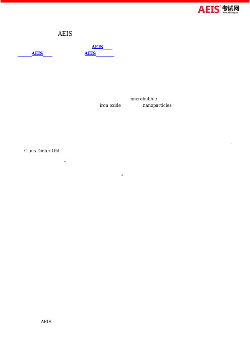
研究员制作出体积只有红血球十分之一的微型气泡(microbubble),然后在外层附上一层抗癌药和氧化铁(iron oxide)纳米颗粒(nanoparticles)。
他们以老鼠做试验,把气泡注射入移植到鼠身上的癌肿瘤后,再放一块磁铁在肿瘤外,就能把附着了氧化铁的气泡吸引到肿瘤四周。
接着,用超声波致使老鼠体内的气泡剧烈颤动,并释放强大能量。
这股能量把抗癌药直接射入癌细胞内层,过程只须百分之一秒。
这项研究由南大化学与生物医学工程学院助理教授徐臣杰博士和南大数理科学学院副院长克劳斯戴德·欧(Claus-Dieter Ohl)副教授联合率领的研究团队负责。
徐臣杰受访时说:“我们研究出能在数毫秒之内,把药物颗粒射入肿瘤内层的方法,这是前所未见的。
药物可嵌入至少50个细胞层的深度,也就是200微米,约头发直径的一倍。
” 在化疗过程中,注入病患血管内的抗癌药会同时杀死癌细胞和健康细胞,药物也无法深入细胞内层,因此体内可能残留一些癌细胞导致肿瘤复发。
此外,部分药物也会通过肺和肝脏排出体外,疗效有限。
南大的新疗法针对性比化疗更强,抗癌药直接命中癌细胞,治疗时间可缩短40%。
此外,健康细胞不会受到破坏,所用的氧化铁和超声波也对人体无害。
不过,这种疗法较适合晚期癌症病患,因为癌肿瘤位置比初期癌症更为集中,这样才能清楚放置磁铁的位置,以吸引药物气泡。
细胞膜仿生铁-硅纳米颗粒用于增强声动力癌症治疗摘要:近年来,癌症治疗已经成为许多研究人员所关注的焦点。
科学家们一直在寻找新的治疗方法,以期提高癌症治疗的效果。
细胞膜仿生铁-硅纳米颗粒作为一种新型的治疗方法,受到了众多研究人员的关注。
本文旨在探寻细胞膜仿生铁-硅纳米颗粒的治疗机制及其在增强声动力癌症治疗中的应用。
关键词:细胞膜仿生铁-硅纳米颗粒、癌症治疗、声动力治疗、治疗机制、临床应用随着科技的不断发展,人们对癌症治疗效果的期望也越来越高。
声动力治疗作为一种新型的癌症治疗方法,其利用声波和化疗药物合作,使药物在细胞内得以快速渗透和吸收。
而细胞膜仿生铁-硅纳米颗粒则成为了这项技术的重要支撑。
细胞膜仿生铁-硅纳米颗粒作为一种新型的药物载体,其表面可覆盖人体细胞的膜,从而在治疗过程中模拟人体自然状态,与细胞表面形成较强的黏附力,能够将药物高效稳定地释放在细胞内,提高药物在体内的生物利用度,加强对癌细胞的打击效果。
此外,细胞膜仿生铁-硅纳米颗粒具有高度的生物相容性和生物降解性,可以降低药物在人体内的副作用,对治疗患者的健康和安全具有极大的帮助。
而细胞膜仿生铁-硅纳米颗粒的临床应用也在不断地拓展。
通过声动力治疗手段,将细胞膜仿生铁-硅纳米颗粒与肿瘤靶向治疗相结合,可以在药物的作用下,直接杀死癌细胞。
同时,在治疗中可以根据患者的情况进行调整,减少对患者的副作用,提高治疗效果。
细胞膜仿生铁-硅纳米颗粒的成熟与发展,为声动力癌症治疗带来了希望。
继续研究和探索这一新型药物载体的性质和特征,对于提高癌症治疗效果、降低药物副作用有着非常重要的意义。
总之,细胞膜仿生铁-硅纳米颗粒以其独特的优势,在癌症治疗领域引起了广泛的关注。
在未来的研究中,我们希望能够通过不断地探索和创新,将其最大限度地应用到临床治疗中,为患者带来更多的福音。
细胞膜仿生铁-硅纳米颗粒作为一种新型的药物载体,在癌症治疗领域具有广阔的应用前景。
其主要具有以下优势:1. 高效稳定的药物释放能力:细胞膜仿生铁-硅纳米颗粒表面可覆盖人体细胞的膜,与细胞表面形成较强的黏附力,从而可以将药物高效稳定地释放在细胞内,提高药物在体内的生物利用度,加强对癌细胞的打击效果。
专利名称:萘醌磷酰胺类化合物及其在作为细胞铁死亡诱导剂中的用途
专利类型:发明专利
发明人:尹玉新,宁显玲,齐海龙
申请号:CN201710160679.4
申请日:20170317
公开号:CN107118231A
公开日:
20170901
专利内容由知识产权出版社提供
摘要:本发明公开了一系列萘醌磷酰胺类化合物及其在作为细胞铁死亡诱导剂中的用途。
所述的萘醌磷酰胺类化合物具有通式I所示的结构。
研究表明,该化合物能够诱导细胞发生铁死亡,进而达到抑制细胞,特别是肿瘤细胞增殖的目的。
本发明提出了一种新型的细胞铁死亡诱导剂,也为肿瘤疾病的治疗提供了一种新的技术手段。
申请人:北京大学
地址:100191 北京市海淀区学院路38号北京大学医学部
国籍:CN
代理机构:北京科龙寰宇知识产权代理有限责任公司
更多信息请下载全文后查看。
2006年12月第32卷第12期北京航空航天大学学报Journa l o f Be iji ng U nivers it y of A eronauti cs and A stronauti cs D ecember 2006V o.l 32 N o 112收稿日期:2006-05-15基金项目:国家科技攻关计划资助项目(2005DFBA0005)作者简介:姚 璐(1982-),女,浙江宁波人,硕士生,Lh64@buaa .edu .cn.低强度超声波改善微生物燃料电池产电效能姚 璐 李正龙(北京航空航天大学材料科学与工程学院,北京100083)刘 红(北京航空航天大学生物工程系,北京100083)摘 要:微生物燃料电池(M FC s ,M icr obia lFue lC ells)可在处理有机废水的同时获得电能,但生物体系缓慢的电子传递速率是其发展的瓶颈.为了寻求提高M FC s 工作效率的途径,建立了2个有效容积为1.5L,电极面积160c m 2的单室MFCs ,设置为超声波强化反应器和对照反应器,进行对比试验.结果表明,采用强度为0.2W /c m 2、频率33k H z 、超声间隔为83h 的超声波对反应器辐照10m i n ,在反应后期(运行2880h 后)M FC s 与对照反应器相比最大功率密度提高了6%,一个运行周期产生的总电量增加了46.5%;设置超声的反应器库仑效率(CE ,Coulo m bic E ffic i e ncy)比对照反应器提高了25.7%.超声波强化反应器中水的pH 值最小值比对照p H 值最小值低0.2,超声波辐照的反应器氧化还原电位(ORP ,Ox idation Reduction Po tentia l)最小值低于对照反应器ORP 最小值34.8mV.2个反应器3000m i n 对化学需氧量(COD,Che m ica lOxygen De m and)的净化效率都达到72.9%,超声波对COD 去除贡献不明显,并从低强度超声波对微生物作用的过程方面分析了上述现象.关 键 词:微生物燃料电池;超声波;葡萄糖;功率密度中图分类号:X 703.1文献标识码:A 文章编号:1001-5965(2006)12-1472-05Im prove el e ctri c it y generati o n ofm i c robi a l f ue l ce ll s by l o w i n t ens ity ultrasoundY ao LuLi Zheng l o ng(School ofM ateri als Science and Engi n eeri ng ,Beiji ng U n i vers it y of Aeronau tics and Astronau tics ,Beiji ng 100083,C h i na)Liu H ong(Dep t .of B i o l og i cal Eng i neeri ng ,Beijing Un i versit y ofAeronauti cs and As tronau tics ,B eiji ng 100083,Ch i na)Abstract :It is possi b le to produce e lectricity i n m icrobial fuel cells(MFCs)w h ile acco mp lish i n g b i o log ica l w aste w ater treat m en,t but sl o w electron transference li m its the develop m ent ofM FC s .To i m prove the e lectric-i ty generati o n ,t w o si m ilar si n g le cha m beredMFCs w ere bu il,t wh ich had the available vo l u m e 1.5L ,and each electr ode area w as 160c m 2.One w as irradiated by u ltrasound ,the other used as contro.l The M FC s w as in -duced by u ltrasound at 33kH z i n 10m in w it h the u ltrasound i n tensities of 0.2W /c m 2every 83hours .The re -su lt sho w s that i n the end of t h e reaction(about 2880h),the m ax i m um po w er density o f the u ltrasound trea-t m ent reactor i n creases by 6%co m paring w ith that of the contr o ,l and the tota l coulo m b increases by 46.5%i n one reacti o n cycle .The ultrasound treat m ent reactor c s Cou lo mb ic efficiency(CE )is 25.7%higher t h an that o f t h e contro.l M oreover ,i n theMFCs w ith u ltrasound ,the lo w est pH ofw aste w ater is l o w er than that i n t h e con -tro,l and the lo w est ox idati o n reducti o n potential(ORP)of reacto r is lo w er by 34.8mV.I n 3000m in t h e t w o reactors c re m ova l rate o f che m ica l oxygen de m and(COD )a ll reaches to 72.9%.The u ltrasound irradiation doesn c t i n crease the re m oval rate of COD obv iously .The explanation o f these differences w as given according to the influence of l o w intensity u ltrasound to the m icr oorgan i s m s .Key wor ds :m icr obia l fue l cells(M FC s);u ltrason ic ;g l u cose ;po w er generati o n微生物燃料电池(M FC s,M icrobia lFuelC ells)可用来处理宇宙飞船上的生物排泄物,同时产生的电能可为额定电压较低的仪器供电.在宇航条件下,每人每天如果排出22g尿素,就能够获得47W的电能,电能虽然不高,但足以为宇宙飞船上额定电压较低的小型仪器供电[1].MFCs在特殊微生物的帮助下,利用酶或者微生物作为催化剂,将化学能转化为电能.在解决环境问题的同时,获得高质量的能源[2].但是,生物体系缓慢的电子传递速率使得M FC s的产电效率较低,成为M FCs发展的瓶颈[3].低强度超声波可通过强化微生物活性来提高污水、污泥的生物处理效率[4-7],但是利用其促进MFCs效能的研究未见报道.本文通过试验,研究了低强度超声波对MFCs 的产电效率、最大功率密度、库仑效率和污水化学需氧量(COD,Che m i c alOxygen De m and)去除率的影响,并依据超声波对微生物作用的机理进行了解释.1试验材料与方法1.1污泥与人工配水污泥:取自高碑店污水处理厂厌氧消化池,污泥浓度(M LVSS)为5g/L,p H值约为7,每个反应器中加入300mL.人工配水:分别取矿物质溶液和维他命溶液各12.5mL,加入盐溶液中,继续加水到985mL,加入磷酸盐调整p H值为7.0.盐溶液、矿物质溶液、维他命溶液采用文献[8]配方.1.2MFCs的构造和工作条件采用2个单极室MFCs,一个设置超声波发生器进行辐照处理,另一个为对照.2个反应器的构造和运行参数相同(表1),设置超声波反应器如图1所示,超声波辐照参数见表2.表1M FC s构造和运行参数参数数值外形尺寸/c m25.5@11.4@24.7有效容积/mL1515有效电极面积/c m2160电极材料40%碳载铂电极质子交换膜材料Nafion膜质子交换膜面积/c m2160反应温度/e30污泥浓度(M LVSS)/(g#L-1)5换水制度产电稳定后,间歇进水,每隔83h用人工配水更换反应器中1/3的上清液图1超声波强化M FCs反应器示意图表2超声波辐照参数频率/k H z超声波强度/(W#c m-2)辐照时间/m i n辐照间隔/h330.210831.3分析测试方法和计算方法COD测试采用美国HAC H测定仪,150e消解2h后用硫酸亚铁铵滴定;M L VSS按照标准方法测试[9].根据电池功率密度随外接电阻变化特性(见图2),选择最佳外接电阻R=1008.使用万用表测定电阻两端电压,并使用数据采集系统(P MD-1608FS)将其储存.功率密度P=UIA.其中,U为电压,V;I为电流,A;A为MFCs阳极的面积,m2.产电能力W=Q t0P#A d t,其中t为时间,h,本文一周期为83h.库仑效率[10-11]G CE=C EX/C TH@100%.其中C EX为给定时间间隔内通过电阻的总电量,C EX=Q t i0U i R d t;C TH为去除COD理论产电量,C TH=F b M v.F为法拉第常数,96485C/m o l;b为单位COD理论产生电子数,按每摩尔C OD(葡萄糖)产生4m ol电子计算;M为污水中COD去除量,m o l;v为进水量,L;R为外接电阻,8.图2电池功率密度随外接电阻变化曲线2结果及讨论2.1低强度超声波辐射对MFC s的作用试验采用间歇式进水,图3为超声波强化整1473第12期姚璐等:低强度超声波改善微生物燃料电池产电效能个过程各个产电周期的电压曲线,图4为试验初期(反应器运行稳定后114h 内)、中期(114h~1968h)和后期(1968h~2880h 后)选取有代表性的3组反应周期(进水周期)的产电特性与对照比较.图3和图4可见,超声波强化初期,两反应器产电没有明显差异.设置超声的反应器最大电压为510.9mV,最大功率密度为163.1mW /m 2;对照最大电压为547.2mV,最大功率密度为187.1m W /m 2.超声波强化中期,两反应器的产电性能出现较明显差异,设置超声的反应器最大电压为563.2mV,最大功率密度为198.7m W /m 2;对照最大电压为544.9mV,最大功率密度为185.6m W /m 2.由于功率密度随COD 的增加而增加,试验使用的COD 为500~800m g /L ,相对M i n [10]研究中利用6000~8000mg /L 的COD 产生的最大功率密度可达到225mW /m 2较低,而功率密度差异不大,所以反应器产电能力较高.同时两反应器的能量利用率也出现了一定差异,设置超声反应器的库仑效率为56.6%,比对照提高5.8%.超声波强化后期,设置超声的反应器产电效能显著高于对照,最大电压为545.0mV,最大功率密度为185.6m W /m 2,而对照的最大电压为529.3mV,最大功率密度为175.1mW /m 2.设置超声的反应器产能与对照相比提高了46.5%,设置超声的反应器G CE 提高到72.3%,比对照提高25.57%.M i n [10]的实验中G CE 达到10%~30%,在I eropou l o s[11]的实验中比较3种MFCs 反应器,G CE 为38.1%,45.7%,87.4%,以乙酸为底物的MFCs 的G CE 可达到63%~78%[12],因此试验得到的G CE 相对达到了较高值.不同运行阶段低强度超声波强化M FC s 的效果见表3.可见低强度超声波辐照对M FCs 产电能力有改善作用,而且长时间运行后此作用更显著.图3超声波强化对微生物燃料产电整个过程的影响a 超声波强化初期b 超声波强化中期c 超声波强化后期图4 超声波强化对微生物燃料产电特性的影响表3 低强度超声波强化M FC s 的效果反应时期反应器电压最大值/V 功率密度最大值/(mW #m -2)一周期产能/10-2(W #h)库仑效率/%与对照相比产能提高百分比/%与对照相比库仑效率提高百分比/%初期超声波强化510.9163.170.648.0对照547.2187.172.348.0-2.40中期超声波强化563.2198.765.756.6对照544.9185.664.453.52.1 5.8后期超声波强化545.0185.658.272.3对照529.3175.139.757.646.525.51474北京航空航天大学学报 2006年按照M arcus 和Soti n 理论,电子传递速率是由电势差、重组能和电子供体与受体之间的距离决定的[7],决定生物燃料电池输出功率密度的主要因素是相关的电子传递过程,因此生物体系缓慢的电子传递速率是生物燃料电池发展的瓶颈[13],酶分子蛋白质的外壳也会对从活性中心到电极的直接电子传递产生屏蔽作用[14].而低强度超声波可以有效提高酶的活性,促进细胞的生长与生物合成,以及改变细胞膜和细胞壁的结构[15],可提高细胞膜通透性[16].短时间低强超声波的机械应力可以在细胞表面瞬间造成细小损伤,该损伤伤口很小,容易被自身修复,在其修复过程中,酶的分泌增多,细胞繁殖加快,新陈代谢活性增强[17].因为改变了污水中微生物细胞活性和改善了细胞膜的通透性,使得电子能够更容易地穿透酶分子蛋白质的外壳到达电池阳极,所以本文采用的低强度超声波(0.2W /c m 2)对MFCs 具有增强产电能力的效果.试验结果表明,低强度超声波对M FC s 的强化是一个持续的、长期的过程,长期的低强度超声波间歇作用促使反应器中的微生物产生了一定程度的驯化和进化,使得微生物更适应在处理污水中有机物的同时产电.2.2 反应后期超声波强化对反应器的影响2.2.1 低强度超声波对p H 值的影响M FC s 是利用微生物在厌氧环境下降解有机污染物时产生电子转移的产电装置.有机物的厌氧消化过程有电子和质子的转移,电子(质子)经过传递体系后需要最终电子受体(最终受氢体)来接受.在厌氧消化过程中,有机物仅发生部分氧化,其产物是低分子有机物.在此过程中p H 值和氧化还原电位(ORP)是2个非常关键的因素[18].对比反应后期较有代表性的一个反应周期两反应器p H 值的变化如图5所示.图5 超声波强化对M FCs 中p H 值的影响图5显示设置超声的反应器pH 值(最小为6.1)要明显低于对照(最小为6.3),这说明经低强度超声波强化后的反应器中有机物释放质子和电子的速度加快,因此表现为更低的p H 值.2.2.2 低强度超声波对COD 的影响对比反应后期较有代表性的一个反应周期两反应器COD(C r 浓度)值的变化如图6所示.图6 超声波强化对M FCs 中C OD 值的影响图6可见两反应器3000m in 对COD 的净化效率达到72.9%,说明M FC s 可以在处理污水的同时产生电能.但是两反应器对COD 的去除效果并没有显著的差异,产生这种现象的原因是MFCs 的工作在厌氧消化过程的产氢产酸阶段,强化的结果使反应体系中的游离质子浓度增加,从而p H 值降低,但COD 去除效率变化并不显著.由于刘红研究利用低强度超声波提高厌氧活性污泥结果显示超声波对COD 去除率有明显贡献[7],而本试验得到不同的结果,分析可能由于超声作用主要提高了MFCs 的电子转移速率,表现为电池产电能力的增加,因此对COD 去除率贡献不明显.2.2.3 低强度超声波对ORP 的影响对比反应后期较有代表性的一个反应周期两反应器ORP 值的变化如图7所示.图7 超声波强化对M FC s 的OR P 值的影响图7中设置超声的反应器最小ORP 值(-420.2mV )要明显低于对照反应器(-385.4mV ).厌氧微生物的生存要求较低的ORP 值环境的原因是它们的一些脱氢酶系包括辅酶I 、铁氧还蛋白和黄素蛋白等要求低的ORP值环境才能保持活性.周洪波等人[19]的研究发现,氧化还原电位对发酵产物有强烈影响.在p H值为6,ORP 值为-550~-300mV 时,乙酸和乳1475第12期 姚 璐等:低强度超声波改善微生物燃料电池产电效能酸是主要产物,丁酸浓度随ORP值的升高而降低,而丙酸和甲酸浓度随ORP值升高而增加.说明MFCs的电子传递主要集中于厌氧消化过程的产氢产酸阶段,而超声波强化使产氢产酸反应速度提高,因此表现为更低的pH值和ORP值.图中对照反应器的ORP值在反应末期相对超声强化有明显上升,推测由于超声波改善了厌氧污泥活性,提高了污泥厌氧程度,所以保持ORP值较低的时间较长.3结论1)长期的间歇低强度超声波辐照对提高M FCs的产电能力有明显的效果,在反应后期最大功率密度达到185.6mW/m2,比对照反应器提高了6%,一个进水周期的总产电量提高46.5%;2)低强度超声波辐照降低了M FC s中的p H 值和ORP值,但是对COD的去除率影响不显著;3)M FC s在产电能的同时可以对污水进行有效净化,C OD去除率可达到72.9%,显示了MFCs 巨大的应用潜力.参考文献(References)[1]成都市科学技术学会科普知识大全.微生物燃料电池[EB/0L].h ttp://www.cdk j x.co m/w eb4/extens i ve/sho w ne w s.as p?n e w si d=730[2]L i u H ong,R a mnarayanan R,Logan B.Producti on of electri citydu ri ng w aste w ater treat m ent u si ng a si ngle cha m ber m i crob i al f u-el cell[J].Environ SciT echno,l2004,38:2281-2285[3]W illner I,K atz E.Integrati on of layered redox p rot eins and con-ducti ve s upport s for b ioelectron ic appli cati ons[J].Ange w Che mInt E d,2000,39:1180-1184[4]W ood B E,A l drich H C,Ingra m L O.U l trasound sti m u l atesethanol p roducti on duri ng t h e si m u lt aneou s scarification and f er-m en t ati on of m i xed w aste office paper[J].B iotechnol Prog,1997,13:232-237[5]S chlaf er O,Onyeche T,Bor m ann H,et a.l U l trasound sti m u l ationof m icro-organ is m s f or enhan ced b i odegradati on[J].U ltras onics,2002,40(1-8):25-29[6]刘红,何韵华,张山立,等.微污染水源水处理中超声波强化生物降解有机污染物研究[J].环境科学,2004,25(3):57-60L i u H ong,H e Yunhua,Zh ang Sh an l,i et a.l Organ i c poll u tantsb iodegradati on i n m i cro-poll u ted w at er enh anced by u ltras on ic[J].Env i ronm en tal S ci en ce,2004,25(3):57-60(i n Ch-i nese)[7]刘红,闫怡新,王文燕,等.低强度超声波改善污泥活性[J].环境科学,2005,26(4):124-128L i u H ong,Y an Y i x i n,W angW enyan,et a.l I m prove m en t of the acti v i ty of acti vated sl udge by l ow i ntens it y u ltrasound[J].E nv-ironm ental S ci ence,2005,26(4):124-128(i n Ch i nes e)[8]L i u H,Logan B E.E lectrici ty gen erati on u si ng an air-cat hodes i ngl e cha m berm i crob i al f uel cell i n the p resen ce and ab s en ce ofa proton exchange m e mb ran e[J].Env i ron m en tal Science andTechnol ogy,2004,38:4040-4046[9]高廷耀,顾国维.水污染控制工程(下册)[M].北京:高等教育出版社,1999:177-187Gao T i ngyao,Gu Guo w e.i W ater polluti on contro l engi n eeri ng (second vol um e)[M].B eiji ng:H i gh er Educati on Pres s,1999:177-187(i n Ch i n ese)[10]M i n B,K i m J R,Logan B E.E lectrici ty gen erati on fro m s w i new aste w ater us i ng m icrob i al fuel cell s[J].W ater Research,2005,39:4961-4968[11]Ieropou los I A,Greenm ana J,M el hu i sh C,et a.l C o m parati ves t udy of three types ofm i crob i al f u el cell[J].En z yme and M-icrob i a lTechn ol ogy,2005,37:238-245[12]Oh S E,M i n B,Logan B E.C athode perfor m an ce as a f actori n electri city gen erati on i n m icrob ial fuel cell s[J].E nviron S ciT echno,l2004,38:4900-4904[13]L i u H,Cheng S,Logan B E.Po w er generati on i n f ed-batchm i crob i al f u el cells as a f unction of i on ic strength,te m perat u re,and reactor con fi gurati on[J].Environ Sci Techno,l2005,39(14):5488-5493[14]M arcu s R A,Suti n N.E l ectron tran sf ers i n ch e m istry and bio-logy[J].B ioch i m B iophys Acta,1985,811(3):265-322 [15]P i ttW G,Ross S A.U ltrasound i n creases t he rate of bacteri alcell gro w t h[J].B i otechno lProg,2003,19(3):1038-1044 [16]时兰春,王伯初,杨艳红,等.低强度超声波在生物技术中应用的研究进展[J].重庆大学学报,2005,25(10):139-142Sh i Lanchun,W ang Bochu,Yang Y anhong,et a.l A pp licati onof l o w i ntens it y u ltras ound to b iot echnol ogy[J].Jou r n al of Chongqing Un i versit y,2005,25(10):139-142(i n Ch i n ese) [17]戴传云,王伯初.低功率超声波对微生物发酵的影响[J].重庆大学学报,2003,26(2):15-17DaiChu anyun,W ang B ochu.E ffect of l o w energy u ltrason i c ont h em icroorgan is m fer m en tati on[J].Journal of Chongq i ng Un-iversity,2003,26(2):15-17(i n C h i nese)[18]李刚,杨立中,欧阳峰.厌氧消化过程控制因素及pH和Eh的影响分析[J].西南交通大学学报,2001,10(5):2258-2272Li Gang,Y ang L iz hong,Ouyang Feng.C ontrol fact ors of an ae-rob i c d i ges ti on and eff ect of pH and Eh[J].J ou rnal of Sou t h-w est Jiaot ong Un ivers i ty,2001,10(5):2258-2272(i n Ch-inese)[19]周洪波,Cord-Ruw isch R,陈坚.产酸相中氧化还原电位控制及其对葡萄糖厌氧发酵产物的影响[J].中国沼气,2000,18(4):20-23Zhou H ongbo,Cord-Ruw i sch R,Ch en J i an.The strategy of red-ox potenti al control and it s i n fl uen ce on anaerob ic f er m entati onof g l ucose i n aci dogen ic react or[J].Ch i na B i ogas,2000,18(4):20-23(i n Ch i n ese)(责任编辑:文丽芳)1476北京航空航天大学学报2006年。
《阴离子-π型AIE光敏剂光动力抗癌和抗菌研究》篇一阴离子-π型E光敏剂光动力抗癌和抗菌研究摘要:本文重点研究了阴离子-π型E(聚集诱导发光)光敏剂在光动力抗癌和抗菌领域的应用。
通过合成新型的E光敏剂,并对其性能进行深入研究,为光动力疗法(PDT)在癌症治疗和抗菌领域提供了新的思路和方法。
一、引言随着科技的发展,光动力疗法在医学领域的应用越来越广泛。
其中,E光敏剂因其独特的发光性质,在生物成像、光动力治疗等方面展现出巨大的潜力。
本文着重探讨阴离子-π型E光敏剂在光动力抗癌和抗菌方面的研究进展。
二、阴离子-π型E光敏剂的合成与性质本部分主要介绍阴离子-π型E光敏剂的合成方法和其物理化学性质。
该类光敏剂分子结构中含有的特殊基团赋予其优异的E 效应和光物理性质,如良好的光稳定性、低毒性等。
三、光动力抗癌研究1. 机制探讨:阴离子-π型E光敏剂在光照条件下,能够产生单线态氧等活性氧物质,进而对癌细胞产生杀伤作用。
此外,该类光敏剂还能通过调节细胞内环境,影响癌细胞的生长和转移。
2. 实验研究:本部分通过细胞实验、动物模型等方式,验证了阴离子-π型E光敏剂在光动力抗癌方面的有效性。
实验结果显示,该类光敏剂能够显著抑制肿瘤的生长,且对正常组织细胞的损伤较小。
3. 临床应用前景:结合临床数据和实验结果,分析该类E光敏剂在光动力抗癌领域的应用前景和潜在优势。
四、光动力抗菌研究1. 机制探讨:阴离子-π型E光敏剂对细菌也具有显著的杀伤作用。
该类光敏剂能够破坏细菌的细胞膜结构,进而导致细菌死亡。
此外,该类光敏剂还能产生一定的抗真菌作用。
2. 实验研究:通过体外实验和实际运用案例,探讨了该类E 光敏剂在抗菌领域的实际应用效果。
实验结果表明,该类光敏剂对多种细菌和真菌均有良好的杀灭作用,且对环境友好,无耐药性问题。
3. 应用拓展:结合当前抗菌领域的需求和挑战,分析阴离子-π型E光敏剂在抗菌领域的潜在应用方向和拓展领域。
五、结论与展望本文通过对阴离子-π型E光敏剂在光动力抗癌和抗菌方面的研究,证明了该类光敏剂在生物医学领域的巨大潜力。
Nanoepitaxy to improve the efficiency of InGaN light-emitting diodes K. Y. Zang, S. J. Chua, J. H. Teng, N. S. Ang, A. M. Yong et al.Citation: Appl. Phys. Lett. 92, 243126 (2008); doi: 10.1063/1.2949983View online: /10.1063/1.2949983View Table of Contents: /resource/1/APPLAB/v92/i24Published by the American Institute of Physics.Related ArticlesDroop improvement in blue InGaN/GaN multiple quantum well light-emitting diodes with indium graded last barrierAppl. Phys. Lett. 99, 233501 (2011)Voltage modulated electro-luminescence spectroscopy to understand negative capacitance and the role of sub-bandgap states in light emitting devicesJ. Appl. Phys. 110, 114509 (2011)Junction temperature measurement of light emitting diode by electroluminescenceRev. Sci. Instrum. 82, 123101 (2011)Enhanced efficiency in high-brightness fluorescent organic light emitting diodes through triplet management APL: Org. Electron. Photonics 4, 260 (2011)Enhanced efficiency in high-brightness fluorescent organic light emitting diodes through triplet management Appl. Phys. Lett. 99, 223303 (2011)Additional information on Appl. Phys. Lett.Journal Homepage: /Journal Information: /about/about_the_journalTop downloads: /features/most_downloadedInformation for Authors: /authorsNanoepitaxy to improve the efficiency of InGaN light-emitting diodes K.Y.Zang,a͒S.J.Chua,b͒J.H.Teng,N.S.S.Ang,A.M.Yong,and S.Y.ChowInstitute of Materials Research and Engineering,3Research Link,Singapore117602,Singapore and Centre for Optoelectronics,Department of Electrical and Computer Engineering,National University of Singapore,2Engineering Drive3,Singapore117576,Singapore͑Received18February2008;accepted24May2008;published online20June2008͒InGaN/GaN blue light-emitting diode͑LED͒structures are grown on nanoepitaxial lateralovergrown͑NELO͒GaN template on sapphire substrates by metal organic chemical vapordeposition.Nanopore arrays in SiO2film are fabricated on the underlying GaN using anodicalumina as etch masks,resulting in a nanoporous SiO2mask layer with an average nanoporediameter and interpore distance of60and110nm,respectively.The LED on NELO GaNdemonstrates low defect density,which is revealed by cross-sectional transmission electronmicroscopy.More importantly,the LED on NELO GaN demonstrates a higher output power,oneorder of magnitude higher at80mA,and an enhancement of the emission efficiency compared tothat of the LED on planar GaN.This is mainly attributed to the improvement of light extractionefficiency by random scattering at the interface of the nanoporous SiO2mask.The nanoporous SiO2mask acts as both a threading dislocation reduction layer and a light scattering layer to enhance bothinternal quantum efficiency and external light extraction efficiency.The use of NELO methodimproves both internal quantum efficiency and external quantum efficiency for III-nitrides basedoptoelectronic devices.©2008American Institute of Physics.͓DOI:10.1063/1.2949983͔III-V nitride compound semiconductors͑GaN,InGaN, and AlGaN͒are a major material system in the development of high efficiency ultraviolet͑UV͒,blue,green,and white light-emitting diodes͑LEDs͒and laser diodes͑LDs͒for a variety of applications including general illumination,bio-logical sensors,and data storage.1Though commercial products are already available,ob-taining high efficiency is still one of the big challenges for GaN based optoelectronic devices.The efficiency of InGaN-based LEDs is dependent on internal quantum efficiency ͑int͒and the light extraction efficiency͑out͒.To increase the internal quantum efficiency,threading dislocation͑TD͒density in GaN and InGaN layers needs to be reduced.InGaN and GaN have a high density of TDs ͑ϳ109cm−2͒,because of the large difference in thermal co-efficient of expansion and lattice constant between the GaN and foreign substrates.Although blue LEDs exhibit rela-tively high internal quantum efficiency͑int͒despite the presence of high density of TDs due to the carrier localiza-tion in InGaN,1study shows that the light emission effi-ciency becomes more sensitive to the nonradiative recombi-nation centers at the TDs when shortening the emission wavelength since there is much weaker carrier localization.2,3 Thus,eliminating TDs is essential for high efficient and re-liable optoelectronic and electronic nitride-based devices.4 Epitaxial lateral overgrowth͑ELO͒has been demon-strated as an effective way to reduce the TD density to 106cm−2.5–8UV LEDs and blue LDs with improved effi-ciency have been demonstrated on ELO GaN.9,10However, device has to be fabricated on the wing regions of conven-tional ELO GaN.Also,due to the carrier localization in the InGaN multiple quantum wells͑MQWs͒,it did not appear to act effectively on the efficiency of blue LEDs.To increase the light extraction efficiency͑out͒,as dis-cussed by several researchers,patterned substrate,11,12rough-ening the surface of p-GaN,patterning the p-GaN surface with photonic crystal structures,and roughening GaN inter-face with an in situ SiN x interlayer13were used.14,15The directions of the propagation of light can be changed from regular to random through random scattering at a rough in-terface to enhance the light extraction efficiency of LEDs.We have demonstrated the growth of high quality GaN layers by metalorganic chemical vapor deposition͑MOCVD͒on ordered nanoporous SiO2mask using nanoepitaxial lateral overgrowth͑NELO͒.The NELO GaN exhibits better surface morphology,low TD density,and better optical properties.16 In this letter,we report on the InGaN-based LEDs fab-ricated on the NELO GaN layer.The blue LEDs on NELO GaN showed a reduced TD density,a higher output power, and improved light emission efficiency compared to the con-trol LED.Interestingly,the results indicate that the nano-porous SiO2mask at the interface acts as not only a disloca-tion reduction layer,but also,more importantly,it acts as a scattering layer that enhances the light extraction efficiency of visible light-emitting devices.The LED structures were grown on sapphire substrates using MOCVD.A2m thick Si doped GaN underlying layer wasfirst grown at1050°C.Next,short-range ordered close packed nanopore arrays in SiO2film were fabricated on the underlying GaN by inductively coupled plasma etching using anodic alumina͑AAO͒templates as etch masks,result-ing in a nanoporous SiO2mask layer with an average pore diameter and interpore distances of60and110nm,respec-tively.An n-type NELO GaN layer was then grown over the nanoporous SiO2layer on the surfaces of n-GaN/sapphire ͑0001͒.The detailed NELO GaN growth technique and AAO fabrication technology were described elsewhere.17 InGaN/GaN MQWs active layers comprising of four pairs of3nm thick InGaN well layers and5nm thick GaN barrier layers were then grown on the n-type NELO GaN at a tem-a͒Electronic mail:ky-zang@.sg.b͒Electronic mail:elecsj@.sg.APPLIED PHYSICS LETTERS92,243126͑2008͒0003-6951/2008/92͑24͒/243126/3/$23.00©2008American Institute of Physics92,243126-1perature of 755°C and a chamber pressure of 100Torr.Fol-lowing the InGaN MQWs growth,p -type GaN were then grown at a temperature of 1020°C and a pressure of 60Torr.Trimethylgallium ͑TMGa ͒,trimethylindium ͑TMIn ͒and NH 3were used as the Ga,In,and N sources,respec-tively.SiH 4and Cp 2Mg were used as dopant sources for n -type and p -type,respectively.Figure 1͑a ͒shows the sche-matic of an InGaN LED structure on NELO GaN and Fig.1͑b ͒shows the corresponding cross-sectional scanning elec-tron microscope ͑SEM ͒image of the nanoporous SiO 2mask located between the NELO GaN and the GaN template.A LED on a nonpatterned GaN layer on sapphire substrates was also grown simultaneously as a control sample.The LED chips were fabricated as follows.Parts of the p -GaN and MQWs were first etched to expose the n -type GaN layer and to form a mesa.A 5nm /5nm thick Ni /Au metal layer was annealed at air ambient to form the p metal contact and a 10nm /150nm /20nm /100nm Ti /Al /Ti /Au metal layer was used as n metal contact.The LED chips with the size of ϳ300ϫ300m 2were characterized using two probes for current injection at room temperature.Figure 2shows cross-sectional transmission electron mi-croscopy ͑TEM ͒images of the InGaN MQWs region.The dislocation density in the MQWs and the underlying NELO GaN is greatly reduced by approximately two orders of mag-nitude compared to that of the control sample,which is also consistent with the result of the atomic force microscopy.It can be estimated from the image that the thicknesses of the well and the barrier are ϳ30and 50Å,respectively.The image contrast shows a sharp and flat interface between theInGaN and GaN epilayers,which indicate the good quality of the sample and show good uniformity in the InGaN wells.The dislocations in the InGaN MQWs are known to be non-radiative recombination centers,leading to low quantum ef-ficiency,especially in InGaN based UV-LEDs.The reduction of defects in InGaN MQWs grown on NELO GaN offers a reduced number of nonradiative recombination centers so as to increase the internal quantum efficiency for the future GaN or InGaN-based LEDs.Figure 3shows the room temperature electrolumines-cence ͑EL ͒spectra of the LED on NELO GaN and that on planar GaN at a forward current of 20mA.The peak wave-length and the full width at half maximum of the emission spectra of the LED on NELO were 436and 17.3nm,respec-tively,and that of the control LED were 441and 23.8nm,respectively.The intensity from the LED on NELO GaN is one order of magnitude higher than the emission from the control LED.The results show that EL emission was consid-erably higher in the LED on NELO GaN.In addition,the peak wavelength of the LED on NELO is shorter than that of LED grown on planar GaN.The result is consistent with the photoluminescence results and the high resolution x-ray dif-fraction measurement,probably due to the stress state in the underlying GaN template.Figure 4shows the output power of both LEDs as a function of the forward current.The blue InGaN LED on NELO demonstrates a much higher light output power than that on planar GaN on sapphire.Surpris-ingly,this result is contrary to the result of LED grown on ELO.Nakamura and co-workers reported that InGaN-based blue LEDs on ELO demonstrate the same output power as that on sapphire.9,18However,our blue InGaN LED on NELO shows a much higher output power than the LED grown on planar GaN on sapphire.We believe that,besides the benefit of the reduction in the number of nonradiative recombination centers associated with TDs,another factor contributes more to the enhancement of the output power in our sample.It is known that the low light extraction efficiency of LEDs is due to the fact that a major fraction of internal emitted light is guided and confined inside the LEDsandFIG.1.͑Color online ͒͑a ͒Schematic of an InGaN MQW LED grown on nanoepitaxial lateral overgrown ͑NELO ͒GaN;͑b ͒cross-sectional SEM im-age of InGaN /GaN MQW LED on NELO GaN.The inset is an enlarged SEM image near the nanoporous SiO 2mask.The arrows indicate the nano-SiO 2mask ͑dark contrast at the interface ͒.FIG.2.Cross-sectional TEM images of InGaN MQWs grown on ͑a ͒NELO GaN and on ͑b ͒control planar GaN.InGaN MQWs grown on NELO GaN show sharp interfaces and reduction of TD density compared to the control sample.The inset is a high resolution TEM image of InGaN MQWs on NELO GaN.The thicknessed of the well and the barrier are estimated to be 30and 50Å,respectively.FIG.3.͑Color online ͒Room temperature EL spectra of LED grown on NELO GaN and LED grown on planar GaN at a forward injection current of 20mA,revealing a higher light emission efficiency of the LED on NELO GaN.This is partially due to the reduction of the TD density.The inset images are the photographs of light emission from the EL device at a for-ward current 20mA.finally is lost by absorption.In our case,the nanopore arrays in SiO 2mask at the interface serve as a scattering center,which will enhance the light-extraction efficiency of light-emitting devices.From the cross-sectional SEM image shown in Fig.1,GaN nanorods are grown through the nan-opore windows of the SiO 2mask,with diameter of ϳ60nm and the distance between the nanorods ϳ110nm,as short-range ordered arrays inside the SiO 2mask.The directions of the propagation of light could be changed from regular to random at the interface of the GaN nanorod arrays in the nanoporous SiO 2mask,leading to the enhancement of light extraction in the visible region.Tu et al.also observed the improvement of the LED emission efficiency by random scattering of light on the SiN x nanomask.13It is noted that the SiO 2mask can also be designed and fabricated as a pho-tonic crystal structure,which is beneficial to further im-proved output efficiency for better device performance.14In summary,blue InGaN /GaN MQW LEDs were grown by MOCVD on the reduced-defect density NELO GaN and on a planar GaN layer on sapphire substrates.The blue InGaN /GaN LED on NELO GaN showed a reduction of defect density of about two orders of magnitude.The emis-sion efficiency and output power of a LED on NELO GaN using nanoporous a SiO 2mask are much higher than those of a control LED.The increase in light output is due to animprovement in the light extraction efficiency caused by ran-dom scattering at the rough interface of the GaN nanorod arrays in the nanoporous SiO 2mask and the reduction of the TDs.NELO,using a periodic nanoporous SiO 2mask,is ben-eficial for high efficient LEDs in two ways:one is its effec-tiveness in reducing the TD densities,and the other is the formation of a nanoporous SiO 2layer acting as a light scat-tering layer,which enhances the light extraction efficiency.1S.Nakamura,S.Pearton,and G.Fasol,The Blue Laser Diode ͑Springer,Berlin,2000͒.2H.Amano,S.Takanami,M.Iwaya,S.Kamiyama,and I.Akasaki,Phys.Status Solidi A 195,491͑2003͒.3N.Sharma,P.Thomas,D.Tricker,and C.Humphreys,Appl.Phys.Lett.74,2319͑1999͒.4F.A.Ponce,D.B.Bour,W.Gootz,and P.J.Wright,Appl.Phys.Lett.68,57͑1996͒.5S.Nakamura,M.Senoh,S.Nagahama,N.Iwasa,T.Yamada,T.Matsushita,H.Kiyoku,Y .Sugimuto,T.Kozaki,H.Umemoto,M.Sano,and K.Chocho,Appl.Phys.Lett.72,211͑1998͒.6A.Sakai,H.Sunakawa,A.Kimura,and ui,Appl.Phys.Lett.76,442͑2000͒.7O.Nam,M.Bremser,T.S.Zheleva,and R.F.Davis,Appl.Phys.Lett.71,2638͑1997͒.8A.Chakraborty,S.Keller,C.Meier,B.A.Haskell,S.Keller,P.Waltereit,S.P.DenBaars,S.Nakamura,J.S.Speck,and U.K.Mishra,Appl.Phys.Lett.86,031901͑2005͒.9T.Mukai and S.Nakamura,Jpn.J.Appl.Phys.,Part 138,5735͑1998͒.10S.Nakamura,M.Senoh,S.Nagahama,T.Matsushita,H.Kiyoku,Y .Sugimoto,T.Kozaki,H.Umemoto,M.Sano,and T.Mukai,Jpn.J.Appl.Phys.,Part 238,L226͑1999͒.11A.Bell,R.Liu,F.A.Ponce,H.Amano,I.Akasaki and D.Cherns,Appl.Phys.Lett.82,349͑2003͒.12K.Tadatomo,H.Okagawa,Y .Ohuchi,T.Tsunekawa,Y .Imada,M.Kato and T.Taguchi,Jpn.J.Appl.Phys.,Part 240,L583͑2001͒;I.Schnitzer,E.Yablonovitch,C.Caneau,T.J.Gmitter,and A.Scherer,Appl.Phys.Lett.63,2174͑1993͒;M.Yamada,T.Mitani,Y .Narukawa,S.Shioji,I.Niki,S.Sonobe,K.Deguchi,M.Sano and T.Mukai,Jpn.J.Appl.Phys.,Part 241,L1431͑2002͒.13R.-C.Tu,C.-C.Chuo,S.-M.Pan,Y .-M.Fan,C.-E.Tsai,T.-C.Wang,C.-J.Tun,G.-C.Chi,B.-C.Lee,and C.-P.Lee,Appl.Phys.Lett.83,3608͑2003͒.14T.N.Oder,K.H.Kim,J.Y .Lin,and H.X.Jiang,Appl.Phys.Lett.84,466͑2004͒.15C.F.Lin,J.H.Zheng,Z.J.Yang,J.J.Dai,D.Y .Lin,C.Y .Chang,i,and C.S.Hong,Appl.Phys.Lett.88,083121͑2006͒.16K.Y .Zang,Y .D.Wang,S.J.Chua,and L.S.Wang,Appl.Phys.Lett.87,193106͑2005͒.17Y .D.Wang,K.Y .Zang,S.J.Chua,S.Tripathy,H.L.Zhou,and C.G.Fonstad,Appl.Phys.Lett.88,211908͑2006͒.18T.Mukai,K.Takekawa,and S.Nakamura,Jpn.J.Appl.Phys.,Part 237,L839͑1998͒.FIG.4.Relative output power of LEDs as a function of forward current.LEDs on NELO GaN show a much higher output power,which is attributed principally to the light extraction enhancement by random scattering at the interface of the nanoporous SiO 2masks.。