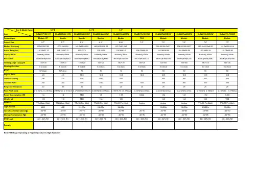
LCD量产规格书
- 格式:xls
- 大小:49.50 KB
- 文档页数:2
Product Description: 65" Full HD Color TFT-LCD ModuleAUO Model Name: P645HW03 V0Customer Part No. / Project Name:Customer Signature AU Optronics Corp.Approved by: PM HeadMichael GoanReviewed by: RD HeadReviewed by: Project LeaderMingyu WuPrepared by: PMAntonio Kuo NoteRev.1.0Date: 2010/07/28Product Functional Specification65" Full HD Color TFT-LCD ModuleModel Name: P645HW03 V0(*) Preliminary Specification() Final Specification Note: This specification is subject to change without notice.Contents NoCONTENTSRECORD OF REVISIONS1 GENERAL DESCRIPTION2 ABSOLUTE MAXIMUM RATINGS3 ELECTRICAL SPECIFICATION3.1 SIGNAL ELECTRIACL CHARACTERISTICS3.2 SIGNAL INTERFACE CONNECTOR3.3 SIGNAL TIMING SPECIFICATION3.4 SIGNAL TIMING WAVEFORM3.5 COLOR INPUT DATA REFERENCE3.6 BACK LIGHT POWER SPECIFICATION3.7 POWER SEQUENCE4 OPTICAL SPECIFICATION5 MECHANICAL CHARACTERISTICS6 PACKING7 RELIABILITY TEST8 INTERNATIONAL STANDARD9 PRECAUTIONSReData Page Items New Description Remark v.0.0 2010/4/20 First Draft1.0 2010/0728 5 Total Power Consumption 440 => 4037~20 3. Electrical Specification New format with modified datahighlighted in red21 Response time 6.5 ms=>8 ms25~26 Drawing Front & Rear views in 1 frame=> Front& Rear views in separate frames1. General DescriptionThis specification applies to the 65 inch Color TFT-LCD Module P645HW03 V0. This LCD module has a TFT active matrix type liquid crystal panel 1920x1080 pixels, and diagonal size of 64.5 inch. This module supports Full HD mode (non-interlace).Each pixel is divided into Red, Green, and Blue sub-pixels or dots which are arranged in vertical stripes. Gray scale or the brightness of the sub-pixel color is determined by 10-bit gray scale signal for each dot.The P645HW03 V0 has been designed to apply the 10-bit 2-channel LVDS interface method. It is intended to support displays where high brightness, wide viewing angle, and high color depth are important.The P645HW03 V0 is RoHS verified which can be distinguished on panel label.General InformationItems Specification Unit NoteActive Screen Size 64.5 inches DiagonalDisplay Area 1428.48 (H) x 803.52 (V) mmOutline Dimension 1482.4(V) x 862.0(H) x 58.9(D) mm With inverterDriver Element a-Si TFT active matrixDisplay Colors 1073.4M (10-bit) colorsColor Gamut 72 % NTSCNumber of Pixels 1920 x 1080 pixelPixel Arrangement RGB vertical stripePixel Pitch 0.744 mmDisplay Mode Transmissive, Normally BlackSurface Treatment Anti-glare, 3HTotal Power Consumption 403(typ.) W include BLU & Signal Life Time (minimum) 50,000 hours 1RoHS RoHS complianceDisplay Orientation Portrait/Landscape enableNote 1: The life is determined as the time at which luminance of the lamp is 50% compared to that of initial value at the typical lamp current on condition of horizontally continuous operating at25±2°C.2. Absolute Maximum RatingsThe followings are maximum values which, if exceeded, may cause faulty operation or damage to the unit:Item Symbol Min. Max Unit Note Logic/LCD Drive Voltage V CC-0.3 +14.0 V 1Input Voltage of Signal V IN-0.3 +4.0 V 1BLU Input Voltage V DDB-0.3 +27.0 V 1On/Off control voltage V BLON-0.3 +5.5 V 1Operating Temperature T OP0 +50 °C 2Operating Humidity H OP10 90 %RH 2Storage Temperature T ST-20 +60 °C 2Storage Humidity H ST10 90 %RH 2Open Lamp Voltage V FB-0.3 +3.6 VPanel Surface Temperature T SUR- +65 °C 2Note 1: If operate over spec but under absolute maximum rating, duration must be < 50ms.Note 2: Maximum Wet-Bulb should be 39°C and no condensation. The relative humidity must not exceed 80% non-condensing at temperatures of 40°C or less. At temperatures greater than40°C, the wet bulb temperature must not exceed 39°C. When operate at low temperatures,the brightness of CCFL will drop and the life time of CCFL will be reduced.3. Electrical SpecificationThe P645HW03 V0 requires two power inputs. One is employed to power the LCD electronics and to drive the TFT array and liquid crystal. The second input which powers the CCFL, is typically generated by an inverter.3.1 Signal Electrical Characteristics 3.1.1: DC CharacteristicsValueParameterSymbol Min. Typ. Max Unit Note Power Supply Input Voltage V DD 10.8 12 13.2 V DC Power Supply Input Current I DD -- 0.58 TBD A 1 Power Consumption P C -- 6.96 TBD Watt 1 Inrush CurrentI RUSH -- -- TBD A 2 Input Differential Voltage∣V ID ∣200 400 600 mV DC 3 Differential Input High Threshold Voltage V TH +100 -- +300 mV DC 3 Differential Input Low Threshold Voltage V TL -300 -- -100 mV DC 3 LVDS InterfaceInput Common Mode VoltageV ICM 1.1 1.25 1.4 V DC 3 Input High Threshold Voltage V IH (High) 2.7 -- 3.3 V DC 4 CMOS InterfaceInput Low Threshold VoltageV IL (Low)--0.6V DC43.1.2: AC CharacteristicsValueParameterSymbol Min. Typ. Max Unit Note Receiver Clock : Spread Spectrum Modulation rangeFclk_ss Fclk -3% -- Fclk +3% MHz 5 Receiver Clock : Spread SpectrumModulation frequencyFss30 -- 200 KHz5LVDSInterfaceReceiver Data Input MargintRMG -0.4--0.4ns 6Note :1. V DD = 12.0V, Fv = 60Hz, Fclk= 82MHz , 25 , Test Pattern : White Pattern ℃ 2. Measurement condition : Rising time = 400usDD3. V ICM = 1.25VID |V IC G N 0VL V D S -L V D S +4. The measure points of V IH and V IL are in LCM side after connecting the System Board and LCM.5. LVDS Receiver Clock SSCG (Spread spectrum clock generator) is defined as below figuresFclk Fclk__ss ss((max max))Fclk Fclk__ss ss((min min))Fclk6. Receiver Data Input MarginRatingParameterSymbol Min Type Max Unit Note Input Clock Frequency Fclk Fclk (min) -- Fclk (max) MHz T=1/Fclk Input Data Position0 tRIP1 -|tRMG| 0 |tRMG| ns Input Data Position1 tRIP0 T/7-|tRMG| T/7 T/7+|tRMG| ns Input Data Position2 tRIP6 2T/7-|tRMG| 2T/7 2T/7+|tRMG| ns Input Data Position3 tRIP5 3T/7-|tRMG| 3T/7 3T/7+|tRMG| ns Input Data Position4 tRIP4 4T/7-|tRMG| 4T/7 4T/7+|tRMG| ns Input Data Position5 tRIP3 5T/7-|tRMG| 5T/7 5T/7+|tRMG| ns Input Data Position6 tRIP26T/7-|tRMG|6T/76T/7+|tRMG|ns3.2 Signal Interface ConnectionsLCD connector: FI-RE51S-HF (Manufactured by JAE)Mating connector: FI-RE51S-HL (Manufactured by JAE)No. Symbol Description No. Symbol Description1 VCC +12V Power Supply 27 RXEN1 LVDS Even pixel data input pair 1(-)2 VCC +12V Power Supply 28 RXEP1 LVDS Even pixel data input pair 1(+)3 VCC +12V Power Supply 29 RXEN2 LVDS Even pixel data input pair 2(-)4 VCC +12V Power Supply 30 RXEP2 LVDS Even pixel data input pair 2(+)5 VCC +12V Power Supply 31 GND Ground6 GND Ground 32 RXENCLK LVDS Even pixel clock input pair(-)7 GND Ground 33 RXEPCLK LVDS Even pixel clock input pair(+)8 GND Ground 34 GND Ground9 GND Ground 35 RXEN3 LVDS Even pixel data input pair 3(-)10 RXON0 LVDS Odd pixel data input pair 0(-) 36 RXEP3 LVDS Even pixel data input pair 3(+)11 RXOP0 LVDS Odd pixel data input pair 0(+) 37 RXEN4 LVDS Even pixel data input pair 4(-)12 RXON1 LVDS Odd pixel data input pair 1(-) 38 RXEP4 LVDS Even pixel data input pair 4(+)13 RXOP1 LVDS Odd pixel data input pair 1(+) 39 GND Ground14 RXON2 LVDS Odd pixel data input pair 2(-) 40 NC No connected15 RXOP2 LVDS Odd pixel data input pair 2(+) 41 NC No connected16 GND Ground 42 NC No connected17 RXONCLK LVDS Odd pixel clock input pair(-) 43 NC No connected18 RXOPCLK LVDS Odd pixel clock input pair(+) 44 NC No connected19 GND Ground 45 LVDSORD Select LVDS data order: High or NC → NSLow → JEIDA20 RXON3 LVDS Odd pixel data input pair 3(-) 46 Reserved AUO Internal Use Only21 RXOP3 LVDS Odd pixel data input pair 3(+) 47 Reserved AUO Internal Use Only22 RXON4 LVDS Odd pixel data input pair 4(-) 48 Reserved AUO Internal Use Only23 RXOP4 LVDS Odd pixel data input pair 4(+) 49 Reserved AUO Internal Use Only24 GND Ground 50 Reserved AUO Internal Use Only25 RXEN0 LVDS Even pixel data input pair 0(-) 51 Reserved AUO Internal Use Only26 RXEP0 LVDS Even pixel data input pair 0(+)Note 1: All GND (ground) pins should be connected together and should also be connected to the LCD’s metal frame.Note 2: All V DD (power input) pins should be connected together.Note 3: All NC (no connection) pins should be open without voltage input.Model Name: P645HW03 V0 Product SpecificationLVDS Option = Open/High(3.3V)P re v io u s C y c le C lo c kNSC u rre n t C y c le N e x t C y c leC H x_0+ C H x_0-R1R0G0R5R4R3R2R1R0G0C H x_1+ C H x_1-G2G1B1B0G5G4G3G2G1B1C H x_2+ C H x_2-B3B2DENANAB5B4B3B2DEC H x_3+ C H x_3-R7R6NAB7B6G7G6R7R6NAC H x_4+ C H x_4-R9R8NAB9B8G9G8R9R8NANote: x = 1, 2, 3, 4…LVDS Option = Low(GND)P re v io u s C y c le C lo c kJEIDAC u rre n t C y c le N e x t C y c leC H x_0+ C H x_0-R5R4G4R9R8R7R6R5R4G4C H x_1+ C H x_1-G6G5B5B4G9G8G7G6G5B5C H x_2+ C H x_2-B7B6DENANAB9B8B7B6DEC H x_3+ C H x_3-R3R2NAB3B2G3G2R3R2NAC H x_4+ C H x_4-R1R0NAB1B0G1G0R1R0NANote: x = 1, 2, 3, 4…©Copyright AU Optronics Corp. 2010 All Rights Reserved No Reproduction and Redistribution AllowedP645HW 03 V0Page 11/34Model Name: P645HW03 V0 Product Specification3.3 Signal Timing SpecificationThis is the signal timing required at the input of the user connector. All of the interface signal timing should be satisfied with the following specifications for its proper operation.Timing Table (DE only Mode) Signal Item Period Vertical Section Active Blanking Period Horizontal Section Active Blanking Clock Vertical Frequency Horizontal Frequency Notes: (1) Display position is specific by the rise of DE signal only. Horizontal display position is specified by the rising edge of 1 DCLK after the rise of 1 DE, is displayed on the left edge of the screen. (2)Vertical display position is specified by the rise of DE after a “Low” level period equivalent to eight times of horizontal period. The 1 data corresponding to one horizontal line after the rise of 1 DE is displayed at the top line of screen. (3)If a period of DE “High” is less than 1920 DCLK or less than 1080 lines, the rest of the screen displays black. (4)The display position does not fit to the screen if a period of DE “High” and the effective data period do not synchronize with each other.st st st stSymbol Tv Tdisp (v) Tblk (v) Th Tdisp (h) Tblk (h) Fclk=1/Tclk Fv FhMin. 1090Typ. 1125 1080Max 1480Unit Th Th10 103045 1100 960400 1325Th Tclk Tclk70 50 47 60140 74.25 60 67.5365 82 63 73Tclk MHz Hz KHzFrequency Frequency Frequency©Copyright AU Optronics Corp. 2010 All Rights Reserved No Reproduction and Redistribution AllowedP645HW 03 V0Page 12/34Model Name: P645HW03 V0 Product SpecificationTv Tblk(v) Th DE Tdisp(v)M pixelRGB DataInvalid DataLine NLine 1Line 2Line 3Line 4Line NInvalid DataN L in eCLK Tclk Th Tdisp(h) DETblk(h)CH1Pixel M-7Pixel M-5Pixel M-3Pixel M-1Invalid DataPixel 1Pixel 3Pixel 5Pixel 7Pixel 9Pixel 11Pixel M-5Pixel M-3Pixel M-1Invalid DataPixel 1Pixel 3CH2Pixel M-6Pixel M-4Pixel M-2Pixel MInvalid DataPixel 2Pixel 4Pixel 6Pixel 8Pixel 10Pixel 12Pixel M-4Pixel M-2Pixel MInvalid DataPixel 2Pixel 4©Copyright AU Optronics Corp. 2010 All Rights Reserved No Reproduction and Redistribution Allowed3.4 Signal Timing WaveformP645HW 03 V0Page 13/34Model Name: P645HW03 V0 Product Specification3.5 Color Input Data ReferenceThe brightness of each primary color (red, green, and blue) is based on the 10-bit gray scale data input for the color; the higher the binary input, the brighter the color. The table below provides a reference for color versus data input.Input Color Data REDColorGREEN LSB MSB LSB MSBBLUE LSBMSBR9 R8 R7 R6Black Red(1023) Green(1023) Basic Color Blue(1023) Cyan Magenta Yellow White RED(000) RED(001) RED ---RED(1022) RED(1023) GREEN(000) GREEN(001) GREEN ---GREEN(1022) GREEN(1023) BLUE(000) BLUE(001) BLUE ------BLUE(1022) BLUE(1023)R5 R4 R3 R2 R1 R0 G9 G8 G7 G6 G5 G4 G3 G2 G1 G0 B9 B8 B7 B6 B5 B4 B3 B2 B1 B0 0 1 0 0 0 1 1 1 0 0 0 1 0 0 0 1 1 1 0 0 0 1 0 0 0 1 1 1 0 0 0 1 0 0 0 1 1 1 0 0 0 1 0 0 0 1 1 1 0 0 0 1 0 0 0 1 1 1 0 1 0 0 1 0 1 0 1 1 0 0 0 0 1 0 1 0 1 1 0 0 0 0 1 0 1 0 1 1 0 0 0 0 1 0 1 0 1 1 0 0 0 0 1 0 1 0 1 1 0 0 0 0 1 0 1 0 1 1 0 0 0 0 1 0 1 0 1 1 0 0 0 0 1 0 1 0 1 1 0 0 0 0 1 0 1 0 1 1 0 0 0 0 1 0 1 0 1 1 0 0 0 0 0 1 1 1 0 1 0 0 0 0 0 1 1 1 0 1 0 0 0 0 0 1 1 1 0 1 0 0 0 0 0 1 1 1 0 1 0 0 0 0 0 1 1 1 0 1 0 0 0 0 0 1 1 1 0 1 0 0 0 0 0 1 1 1 0 1 0 0 0 0 0 1 1 1 0 1 0 0 0 0 0 1 1 1 0 1 0 0 0 0 0 1 1 1 0 1 0 00 1 0 0 0 1 1 1 0 00 1 0 0 0 1 1 1 0 00 1 0 0 0 1 1 1 0 00 1 0 0 0 1 1 1 0 01 1 0 01 1 0 01 1 0 01 1 0 01 1 0 01 1 0 01 1 0 01 1 0 01 1 0 00 1 0 00 0 0 00 0 0 00 0 0 00 0 0 00 0 0 00 0 0 00 0 0 00 0 0 00 0 0 00 0 0 10 0 0 00 0 0 00 0 0 00 0 0 00 0 0 00 0 0 00 0 0 00 0 0 00 0 0 00 0 0 00 0 0 00 0 0 00 0 0 00 0 0 00 0 0 00 0 0 00 0 0 00 0 0 00 0 0 00 0 0 01 1 0 01 1 0 01 1 0 01 1 0 01 1 0 01 1 0 01 1 0 01 1 0 01 1 0 00 1 0 00 0 0 00 0 0 00 0 0 00 0 0 00 0 0 00 0 0 00 0 0 00 0 0 00 0 0 00 0 0 00 00 00 00 00 00 00 00 00 00 00 00 00 00 00 00 00 00 00 00 01 11 11 11 11 11 11 11 11 10 1©Copyright AU Optronics Corp. 2010 All Rights Reserved No Reproduction and Redistribution AllowedP645HW 03 V0Page 14/34Model Name: P645HW03 V0 Product Specification3.6 Backlight Power Specification Electrical Specification(Ta=25±5 C, Turn-on after 60mins) Spec Item Input Voltage Input Current Input Power Inrush Current Operating Frequency Symbol VDDB IDDB PDDB IRUSH FBL ON On/Off control voltage VBLON OFF On/Off control current Internal PWM Dimming Control Voltage Internal PWM Dimming Control Current Internal PWM Dimming Ratio External PWM Control Voltage External PWM Control Current External PWM Duty ratio External PWM Frequency IBLON MAX V_IPWM MIN I_IPWM VDDB=24V VDDB=24V 0 0 2 VDC mADC VDDB=24V VDDB=24V 0 0 3.0 0.8 1.5 3.3 mA VDC Condition Min VDDB=24V VDDB=24V VDDB=24V VDDB=24V21.6 15.5oUnit Typ24.0 16.5 396Note 1 1 2 -Max26.4 17.5 431 26.3 TBDVDC ADC W ADC KHz335 TBD422-5.5 VDC-R_IPWMVDDB=24V30 2 0 0 30 140180100 3.3%-MAX VDDB=24V V_EPWM MIN I_EPWM D_EPWM F_EPWM VDDB=24V VDDB=24V VDDB=24V VDDB=24VVDC 0.8 2 100 240 mADC % Hz -©Copyright AU Optronics Corp. 2010 All Rights Reserved No Reproduction and Redistribution AllowedP645HW 03 V0)Page 15/34Note 1 : Dimming ratio= 100% (MAX) Ta=25±5 , Turn on for 45minutes Note 2 : Measurement condition Rising time = 20ms (VDDB : 10%~90%);℃(Model Name: P645HW03 V0 Product Specification Backlight Connector Pin Configuration 1. Input specificationC/BCN1 of Master board: S14B-PH-SM3-TB (JST) or equivalent Pin No 1 2 3 4 5 6 7 8 9 10 11 12 Symbol VDDB VDDB VDDB VDDB VDDB BLGND BLGND BLGND BLGND BLGND NC VBLON Description Operating Voltage Supply, +24V DC regulated Operating Voltage Supply, +24V DC regulated Operating Voltage Supply, +24V DC regulated Operating Voltage Supply, +24V DC regulated Operating Voltage Supply, +24V DC regulated Ground and Current Return Ground and Current Return Ground and Current Return Ground and Current Return Ground and Current Return No connect Backlight On/Off: Open/High(+3.3V) for BL on, Low(GND) for BL off External PWM Dimming Control input; 13 PDIM(1)Open/High (3.3V/100% Duty) for 100% Lum Internal PWM Dimming Control Input: Open/High (3.3V) for 100% Lum; GND for 30% Lum14PDIM Selection(2,3)Dimming mode Selection. Low(GND)/Open: External PWM dimming; High(3.3V): Internal PWM dimming.Note 1: PDIM is PWM duty control input for +3.3V TTL level signal or DC voltage by Pin 14 input. This input signal is (a) continuous pulse signal with +3.3V, 100% duty (i.e. +3.3V, DC level), backlight should perform 100% luminance. Duty ratio of this input signal should be proportional relationship in certain range of control without any©Copyright AU Optronics Corp. 2010 All Rights Reserved No Reproduction and Redistribution Allowed P645HW 03 V0 Page 16/34Model Name: P645HW03 V0 Product Specification kind of inherent side effect like waterfall effect on screen. Guaranteed duty range and dimming ratio should be specified with supplementary measurement result. Note 2: Pin 14 is the selection pin for dimming control method; if this pin is connected to High , PDIM (Pin 13) input should have DC level signal. Therefore the inverter should have SAW Tooth Wave Generator to generate internal PWM signal. If Pin 14 is connected to GND/open, PDIM (Pin 13) input should have external PWM signal.Note 3: Pin 14 selection vs Pin 13 control function table: Pin 13 (Default: Open/High 100%) Pin 14 = GND / open Pin 14 = High External PWM (AC signal control duty) Internal PWM (DC power control duty)CN1 of slave board: S12B-PH-SM3-TB (JST) or equivalent Pin No 1 2 3 4 5 6 7 8 9 10 11 12 Symbol VDDB VDDB VDDB VDDB VDDB VDDB BLGND BLGND BLGND BLGND BLGND BLGND Description Operating Voltage Supply, +24V DC regulated Operating Voltage Supply, +24V DC regulated Operating Voltage Supply, +24V DC regulated Operating Voltage Supply, +24V DC regulated Operating Voltage Supply, +24V DC regulated Operating Voltage Supply, +24V DC regulated Ground and Current Return Ground and Current Return Ground and Current Return Ground and Current Return Ground and Current Return Ground and Current Return©Copyright AU Optronics Corp. 2010 All Rights Reserved No Reproduction and Redistribution AllowedP645HW 03 V0Page 17/34Model Name: P645HW03 V0 Product SpecificationCN10 of Master board: S3B-ZR-SM3A-TF (JST) Pin NO. 1 2 3 Note : Open Lamp Detection Configuration: Signal name FB1 FB2 GND Description Feedback pin 1 (Sensor open lamp signal) Feedback pin 2 (Sensor open lamp signal) GRONDLamp status Normal 1 lamp open(FB1, FB2) (L,L) (L,H)Remark No Open Lamp Inverter still work and send alarm signal continually.2~3 lamps open(H,L)Inverter still work and send alarm signal continually.4 lamps open3.7 Power Sequence Power Sequence of LCD90% 90% 10% 10%Pow er Supply For LCD VD D (+ 12 V )G NDInterface Signal ( LV DS Data & CLK )G NDon/ Backlight on / off control signal ( VBLO N )GNDCM O S Interface SignalG NDParameter Min. t1 t2 0.4 0.1 Type. ----P645HW 03 V0©Copyright AU Optronics Corp. 2010 All Rights Reserved No Reproduction and Redistribution Allowed≧(H,H)Inverter shut down10%t1t2t5t6t7Valid D atat3t4t8t9Values Unit Max. 30 50 ms msPage 18/34Model Name: P645HW03 V0 Product Specification t3 t4 t5 t6 t7 t8 t9 450 0*1-----------------------*2ms ms ms ms ms ms ms0 --500 10 0--50 ---Note: (1) t4=0 : concern for residual pattern before BLU turn off. (2) t6 : voltage of VDD must decay smoothly after power-off. (Customer system decide this value) Apply the lamp voltage within the LCD operating range. When the backlight turns on before the LCD operation or the LCD turns off before the backlight turns off, the display may momentarily become abnormal. Caution: The above on/off sequence should be applied to avoid abnormal function in the display. In case of handling, make sure to turn off the power when you plug the cable into the input connector or pull the cable out of the connector.©Copyright AU Optronics Corp. 2010 All Rights Reserved No Reproduction and Redistribution AllowedP645HW 03 V0Page 19/34Model Name: P645HW03 V0 Product SpecificationPower Sequence of Inverter90%24V(typ.)90%Power Input for BLU (VDDB)10%T1T2T5Dimming Control Signal (V_IPWM,V_EPWM) T3 T4BLU On/Off Enable (VBLON)Dip condition for InverterPower Input for BLU (VDDB)T6VDDB(typ.)*0.8Parameter T1 T2 T3 T4 T5 T6Values Min. 20 500 250 0 1 -Typ. ------Max. -----10Unit ms ms ms ms ms ms©Copyright AU Optronics Corp. 2010 All Rights Reserved No Reproduction and Redistribution AllowedP645HW 03 V0Page 20/34Model Name: P645HW03 V0 Product Specification4. Optical SpecificationOptical characteristics are determined after the unit has been ‘ON’ and stable for approximately 60 minutes in a dark environment at 25° The values specified are at an approximate distance 50cm from the LCD surface at a C. viewing angle of φ and θ equal to 0° .Test condition:(Ta=25±5 C, Turn-on after 60mins) Parameter Contrast Ratio Surface Luminance (White) Luminance Variation Response Time (Average) Rising Time Falling Time Color Coordinates Red Rx Ry Green Gx Gy Blue Bx By White Wx Wy Viewing Angle x axis, right(φ=0° ) x axis, left(φ=180° ) y axis, up(φ=90° ) y axis, down (φ=270° ) θr θl θu θd ----89 89 89 89 ----degree degree degree degree Typ.-0.03 TBD TBD TBD TBD TBD TBD 0.28 0.29(Contrast Ratio>10)oSymbol Min. CR LWH δWHITE(9P) TR Tr Tf 3000 550 ---Values Typ. 4000 700 -8 15 8 Max --1.3 -25 10UnitNotes 1cd/m22 3ms ms ms5 (Gray to Gray)4 4Typ.+0.036 6 6 6©Copyright AU Optronics Corp. 2010 All Rights Reserved No Reproduction and Redistribution AllowedP645HW 03 V0Page 21/34Model Name: P645HW03 V0 Product Specification Note: 1. Contrast Ratio (CR) is defined mathematically as: Surface Luminance with all” white” pixels Contrast Ratio(CR) = Surface Luminance with all “black” pixels2. Surface luminance is luminance value at point 1 across the LCD surface 50cm from the surface with all pixels displaying white. From more information see Fig. 4-2. When VDDB = 24V, IDDB = 12.5 A. LWH=Lon1, Where Lon1 is the luminance with all pixels displaying white at center 1 location.2 1 435Fig.4-2 Optical measurement point3. The variation in surface luminance, δWHITE is defined under 100% brightness as: δWHITE(5P)=Maximum(Lon1, Lon2,…,Lon5)/Minimum(Lon1, Lon2,…Lon5)4. Response time is the time required for the display to transition from white(L255) to black(L0) (Decay Time, TrD=Tf) and from black(L0) to white(L255) (Rise Time, TrR=Tr). For additional information see Fig. 4-3.Fig.4-3 Response time©Copyright AU Optronics Corp. 2010 All Rights Reserved No Reproduction and Redistribution AllowedP645HW 03 V0Page 22/34Model Name: P645HW03 V0 Product Specification5. The response time is defined as the following figure and shall be measured by switching the input signal among 0%, 25%, 50%, 75%, 100% luminance. For additional information see Fig. 4-4. 0% 0% 25% 50% 75% 100% t: 25%-0% t: 50%-0% t: 75%-0% t: 100%-0% t: 50%-25% t: 75%-25% t: 100%-25% t: 75%-50% t: 100%-50% t: 100%-75% 25% t: 0%-25% 50% t: 0%-50% t: 25%-50% 75% t: 0%-75% t: 25%-75% t: 50%-75% 100% t: 0%-100% t: 25%-100% t: 50%-100% t: 75%-100%Fig.4-4 Response time 6. Viewing angle is the angle at which the contrast ratio is greater than 10. The angles are determined for the horizontal or x axis and the vertical or y axis with respect to the z axis which is normal to the LCD surface. For more information see Fig. 4-5. (Optical measurement by SR3)Fig.4-5 Viewing Angle Definition©Copyright AU Optronics Corp. 2010 All Rights Reserved No Reproduction and Redistribution AllowedP645HW 03 V0Page 23/34Model Name: P645HW03 V0 Product Specification5. Mechanical CharacteristicsThe contents provide general mechanical characteristics for the model P645HW03 V0. Detailed mechanical drawings are shown in the following pages.Horizontal (typ.) Outline Dimension Vertical (typ.) Depth (typ.) Bezel Opening Area Horizontal (typ.) Vertical (typ.) Horizontal Vertical 30 KG (Max)1482.4 mm 862.0 mm 58.9mm (with inverter) 1440.6mm 814.6 mm 1428.48 mm 803.52 mmActive Display Area Weight©Copyright AU Optronics Corp. 2010 All Rights Reserved No Reproduction and Redistribution AllowedP645HW 03 V0Page 24/34Model Name: P645HW03 V0 Product Specification 2D Drawing (Front)©Copyright AU Optronics Corp. 2010 All Rights Reserved No Reproduction and Redistribution AllowedP645HW 03 V0Page 25/34Model Name: P645HW03 V0 Product Specification 2D Drawing (Rear)©Copyright AU Optronics Corp. 2010 All Rights Reserved No Reproduction and Redistribution AllowedP645HW 03 V0Page 26/34Model Name: P645HW03 V0 Product Specification Packing6. Reliability TestNo 1 2 3 4 Test Item High temperature storage test Low temperature storage test Condition Ta=60 , 300hr judge Ta=-20 , 300hr judgeHigh temperature operation test Ta=50 , 300hr judge Low temperature operation test Ta=-5 , 300hr judge Vibration test (with carton) Drop test (with carton) Wave form: Random Vibration level: 1.5G RMS, Bandwidth: 10~200Hz Duration: X, Y, Z (30min each direction) Bottom flats:25.4 cm (ASTMD4169-I)56©Copyright AU Optronics Corp. 2010 All Rights Reserved No Reproduction and Redistribution AllowedP645HW 03 V0℃ ℃ ℃ ℃Page 27/34Model Name: P645HW03 V0 Product Specification7. International Standard7.1 Safety(1) UL60065,2003, Underwriters Laboratories, Inc. (AUO file number : E204356) Audio, video and similar electronic apparatus, safety requirement (2) UL60950-1,2003, Underwriters Laboratories, (AUO file number : E204356) Standard for safety of information technology equipment including electrical business equipment (3) EN60065 (4) EN60950 (5) IEC 60065, European Committee for Electro technical Standardization (CENELEC) Audio, video and similar electronic apparatus, safety requirement (6) IEC 60950-1: European Committee for Electrotechnical Standardization (CENELEC) European Standard for safety of information technology equipment including electrical business equipment7.2 EMC(1) ANSI C63.4 “Methods of Measurement of Radio-Noise Emissions from Low-Voltage Electrical and Electrical Equipment in the Range of 9kHz to 40GHz. “American National standards Institute(ANSI), 1992 (2) C.I.S.P.R “Limits and Methods of Measurement of Radio Interface Characteristics of Information Technology Equipment.” International Special committee on Radio Interference. (3) EN 55022 “Limits and Methods of Measurement of Radio Interface Characteristics of Information Technology Equipment.” European Committee for Electrotechnical Standardization. (CENELEC), 1998©Copyright AU Optronics Corp. 2010 All Rights Reserved No Reproduction and Redistribution AllowedP645HW 03 V0Page 28/34。
7寸LCD规格书Product SpecificationsCustomerDescription 7” TFT LCD ModuleModel Name LS700AT9001Date 2009/07/06Doc. No.Revision 04Customer ApprovalDateThe above signature represents that the product specifications, testing regulation, and warranty in the specifications are acceptedEngineeringCheck Date Prepared DateYang 2009.07.062009.07.06 SimonHead Office & Factory : No. 12, Nanke 8th Rd., T ainan Science-Based Industrial Park, Taiwan, 74144 R.O.C.TEL: +886-6-5889980FAX: +886-6-5051522CONTENTSNo. ITEM PAGE REVISION 3OF0 RECORD1 SUMMARY 42 FEATURES 4SPECIFICATIONS 43 GENERAL4 ABSOLUTERATINGS 4MAXIMUMCHARACTERISTICS 55 ELECTRICALCHARATERISTICS 66 DC7 ACCHARACTERISTICS 6-8CHARATERISTIC9-118 OPTICAL9 INTERFACE12-13DIAGRAM 1410 BLOCKASSURANCE1411 QUALITYDRAWING 15~1612 OUTLINE13 PACKAGEINFORMATION1714 PRECAUTIONS 18-19RECORD OF REVISIONSRevision Date PageDescription01 2008/12/10 All New Creation02 2009/05/13 4Add the Front Polarizer Type in the table of general specifications.5Add Max. Current Value into the table ofBacklight Driving for Power Consumption. 5 Fine tune Operating Conditions 6 Fine tune AC Timing Characteristics 03 2009/05/27 8 Add 7.5 Power On / Off Sequence 042009/07/069Modify 8. OPTICAL CHARATERISTIC7 Modify 7.4 Reset Timing 8 Modify 7.5 Power On / Off Sequence1. SUMMARYLS700AT9001 is a transmissive type color active matrix liquid crystal display (LCD), which uses amorphous thin film transistor (TFT) as switching devices. This panel has a 7.0 inches diagonally measured active display area with SVGA (800 RGB x 600) resolution. The following describes the features of this product.2. FEATURESz 7” (diagonal) inch configuration z SVGA (800×600 pixels) resolution3. GENERAL SPECIFICATIONSParameter Specifications Unit LCD size 7(Diagonal) Inch Display mode Normally white, Transmissive type Number of Pixel 800 RGB x 600 Dot Display Color 262k color Active area 141.60(H) x 106.20(V) mm Pixel Pitch 59 (H) x 177 (V) um Pixel Configuration RGB-StripeNTSC 45 % Interface Digital 18bit RGB Polarizer Type(the Front) Anti-Glare Type View Angle L/R/U/D (CR>10) 70,70,50,70 Degree View Angle direction 6 o’clock Outline Dimension 154 (H) x119.2 (V) x 5.1 (D) mm Weight (135) gOperation -10~70℃Temperature RangeStorage -20~80℃4. ABSOLUTE MAXIMUM RATINGSItem Symbol Condition Min. Max. Unit RemarkVcc GND =0 -0.3 6 V -AVDD, GND =0 -0.3 13.5 V - V GH GND =0 -0.3 +42 V -Power Voltage V GL GND =0 VGH-42 +0.3 V -Note :1. All of the voltages listed above are with respective to GND=VSSA=0V2. Device is subject to be damaged permanently if stresses beyond those absolute maximum ratings listed above.5. ELECTRICAL CHARACTERISTICS 5.1. Operating conditions:5.2. Backlight Driving for Power ConsumptionParameter Symbol Min. Typ. Max. Unit Remark LED current I LED - 120 150 mA Note 1 LED voltage V LED 9.0 9.9 - V LED Life Time -10000--HrNote 2ValuesItem SymbolMin. Typ.Max. Unit NoteDigital Power Supply Voltages VCC3.0 3.3 3.6 VDigital Supply Current ConsumptionIVCC - 3040 mA Black Pattern Analog Power Supply Voltage AVDD10.51213.5VAnalog Supply Current ConsumptionIAVDD - 3646 mA Black Pattern Gate Driver Positive Supply VoltageVGH 14 1720 VGate Driver Positive Supply CurrentIVGH - 1 2 mA Black Pattern Gate Driver Negative Supply VoltageVGL -8 -7 -6 VGate Driver Negative Supply CurrentIVGL - 1 2 mA Black Pattern Common Electrode Driving VoltageVCOM - 4.3- V Black PatternInput Logic Signal High ThresholdVIH 0.8Vcc- Vcc VInput Logic Signal Low Threshold VIL 0 - 0.2Vcc VInput levev V1~V5 Vref1 0.4AVDD - AVDD-0.1V Gamma correctionvoltage input Input levev V6~V10 Vref20.1-0.6AVDDVGamma correction voltage input6. DC CHARATERISTICSRatingParameter Symbol Min. Typ. Max.Unit ConditionLow level input voltage V IL 0 - 0.2VCC VHight level input voltage V IH 0.8VCC - VCC V7. AC CHARATERISTICS7.1 AC Timing Characteristics7.2 AC Timing DiagramsSpec.Parameter Symbol Min. Typ. Max.UnitCLK Frequency Fcph - 39.79- MHz CLK Period T cph - 25.13- ns CLK Pulse Duty Tcwh 40 50 60 % DE Period T DEH +T DEL 1000 1056 - Tcph DE Pulse Width T DH - 800 - Tcph DE Frame Blanking T HS 10 28 110 T DEH +T DEL DE Frame Width T EP - 600 - T DEH +T DEL Data Setup Time Tdsu 6 - - ns Data Hold Time Tdhd 6 - - ns DEN Setup Time Tesu 6 - - ns7.3 Data input format7.4 Reset Timing90%RESETBAVDD T>1msVCC7.5 Power On / Off SequenceVCCAVDD Power for LCDT5T3T4<1sT210ms<t1<t210ms<=""></t1<t210ms VGLVGH T1Data SignalGND 100ms<t5,t6< bdsfid="233" p=""></t5,t6<> T4T6Timing Specification:8. OPTICAL CHARATERISTICTa=25±2, ILED=℃120mANote 1: Definition of viewing angle rangeFig. 8-1 Definition of viewing angleItem Symbol Condition Min Typ Max Unit Note TR - 5 10ms Response time TF Θ=0- 15 20ms (2) Contrast ratio CRAt optimizedviewing angle300 400 - - (3) Wx 0.26 0.31 0.36Color Chromaticity White Wy Θ=00.28 0.33 0.38(4) ΘR - 70 -Hor.ΘL - 70 -φH - 50 -Viewing AngleVer.φL CR 10≧ - 70 -Degree (5) Brightness - - (200)250 -cd/m 2 Centerof DisplayNote 2: Test equipment setup:After stabilizing and leaving the panel alone at a driven temperature for 10 minutes, themeasurement should be executed. Measurement should be executed in a stable, windless, and dark room. Optical specifications are measured by Topcon BM-7 luminance meter 1.0° field of view at a distance of 50cm and normal direction.Fig. 8-2 Optical measurement system setupNote 3: Definition of Response time:The response time is defined as the LCD optical switching time interval between “White” state and“Black” state. Rise time, Tr, is the time between photo detector output intensity changed from 90﹪to 10﹪. And fall time, Tf, is the time between photo detector output intensity changed from10﹪to 90﹪.Note 4: Definition of contrast ratio:The contrast ratio is defined as the following expression.Luminance measured when LCD on the “White” state Contrast ratio (CR)=Luminance measured whe n LCD on the “Black” stateNote 5: White Vi = V i50 ± 1.5VBlack Vi = V i50 ± 2.0V“±” means that the analog input signal swings in phase with VCOM signal.“±” means that the analog input signal swings out of phase with VCOM signal.The 100% transmission is defined as the transmission of LCD panel when all the input terminals of module are electrically opened.Note 6: Definition of color chromaticity (CIE 1931)Color coordinates measured at the center point of LCDNote 7: Measured at the center area of the panel when all theinput terminals of LCD panel are electrically opened.9. INTERFACE9.1. LCM PIN DefinitionPinSymbol I/OFunctionRemark1 NC - NC2 NC - NC3 NC - NC4 NC - NC5 NC - NC6 GND I Power Ground7 EDGSL IDefine Input Clock Polarity.When EDGSL=L, Latch Data By Rising Edge of CLK. ( Default Pull Low) When EDGSL=H, CLK Polarity is Inverted, Latch Data by Falling Edge of CLK.8 VCC I Digital Power Supply (+3.3V) 9 V9 I Gamma voltage level 9 10 VGL I Gate OFF power supply voltage 11 V2 I Gamma voltage level 2 12 VGH I Gate ON power supply voltage 13 V6 I Gamma voltage level 614 RESETB I Hardware Global Reset. Low Active. (Default Pull high) 15VCOMICommon electrode voltage input16 GND I Power Ground 17AVDDIAnalog Power Supply18 NC - NC 19 NC - NC 20 V8 I Gamma voltage level 8 21 V5I Gamma voltage level 5 22V3IGamma voltage level 323 GND I Power ground 24R5IRed data (MSB)25 R4 I Red data 26 R3 I Red data 27 R2 I Red data 28 R1 I Red data30 GND I Power ground 31 GND I Power ground 32 G5 I Green data (MSB) 33 G4 I Green data 34 G3 I Green data 35 G2 I Green data 36 G1 I Green data 37 G0 I Green data (LSB)38 DE I Input Data Enable Control.When DE Mode. Active High To Enable Data Input. (Default Pull Low) 39 NC - NC40 GND I Power ground41 DCLK I Clock Signal Input.When CLK=H, User Can Input Different Polarity CLK By EDGSL Setting.When CLK=L, User Can Select CLK Rising Or Dual Edge To Latch By EDGSLSetting.42 VCC I Digital Power Supply (+3.3V)43 NC - NC 44 NC - NC 45B5IBlue data (MSB)46 B4 I Blue data 47 B3 I Blue data 48 B2 I Blue data 49 B1 I Blue data 50 B0 I Blue data (LSB) 51 NC I NC52 V1 I Gamma voltage level 1 53 V4 I Gamma voltage level 4 54 V7 I Gamma voltage level 7 55V10IGamma voltage level 1056 NC - NC 57 NC - NC 58 AVDD I Analog Power Supply59 GND I Power ground60 VCOMICommon electrode voltage input10. BLOCK DIAGRAM11. QUALITY ASSURANCE ***** T a = Ambient TemperatureNote1: The test samples have recovery time for 2 hours at room temperature before thefunction check. In the standard conditions, there is no display function NG issue occurred.Note2: All the cosmetic specifications are judged before the reliability stress.No. Test Items Test Condition REMARK1 High Temperature Storage Test Ta=80 Dry 240h ℃2 Low Temperature Storage Test Ta=-20 Dry 240h ℃3 High Temperature Operation Test T a=70 Dry 240h ℃ 4Low Temperature Operation Test Ta=-10 Dry 240h ℃ 5High Temperature and High HumidityOperation TestTa=60 90%RH 240h ℃ 6 Electro Static Dis charge Test 150pF, 330Ω, ±8KV(Contact)/±15KV(Air), 5 points/panel,5 times/pointNon-operation 7 Thermal Shock Test -10(0.5h) ~ ℃70(0.5h) / 100℃cycles(Dry)8 Vibration Test Sine wave, 10 ~ 500 ~ 10Hz,1.5G, 0.37oct/min 3 axis, 1hour/axis Non-operation9 Mechanical Shock TestHalf sine wave, 180G, 2ms one shock of each six faces(I.e. run 180G 2ms for all six faces)Non-operation 1st ~ 60th12. OUTLINE DRAWING13. PACKAGE INFORMATION14. PRECAUTIONSPlease pay attention to the following when you use this TFT LCD panel with IC and FPC14.1 MOUNTING PRECAUTIONS(1) You must mount a module using arranged in four corners or four sides.(2) You should consider the mounting structure so that uneven force (ex. Twisted stress) is notapplied to the module.And the case on which a module is mounted should have sufficient strength so that external force is not transmitted directly to the module.(3) Please attach a transparent protective plate to the surface in order to protect the polarizer.Transparent protective plate should have sufficient strength in order to the resist external force.(4) You should adopt radiation structure to satisfy the temperature specification.(5) Acetic acid type and chlorine type materials for the cover case are not describe becausethe former generates corrosive gas of attacking the polarizer at high temperature and the latter causes circuit break by electro-chemical reaction.(6) Do not touch, push or rub the exposed polarizers with glass, tweezers or anything harderthan HB pencil lead. And please do not rub with dust clothes with chemical treatment.Do not touch the surface of polarizer for bare hand or greasy cloth. (Some cosmetics are determined to the polarizer)(7) When the surface becomes dusty, please wipe gently with adsorbent cotton or other softmaterials like chamois soaks with petroleum benzene. Normal-hexane is recommended for cleaning the adhesives used to attach front / rear polarizers. Do not use acetone, toluene andalcohol because they cause chemical damage to the polarizer.(8) Wipe off saliva or water drops as soon as possible. Their long time contact with polarizercauses deformations and color fading.(9) Do not open the case because inside circuits do not have sufficient strength.14.2 OPERATING PRECAUTIONS(1) The spike noise causes the mis-operation of circuits. It should be lower than followingvoltage:V=±200mV(Over and under shoot voltage)(2) Response time depends on the temperature. (In lower temperature, it becomes longer.)(3) Brightness depends on the temperature. (In lower temperature, it becomes lower)And in lower temperature, response time (required time that brightness is stable after turned on) becomes longer.(4) Be careful for condensation at sudden temperature change. Condensation makes damageto polarizer or electrical contacted parts. And after fading condensation, smear or spot will occur.(5) When fixed patterns are displayed for a long time, remnant image is likely to occur.(6) Module has high frequency circuits. Sufficient suppression to the electromagneticinterference shall be done by system manufacturers. Grounding and shielding methods may be important to minimize the interference.14.3 ELECTROSTATIC DISCHARGE CONTROLSince a module is composed of electronic circuits, it is not strong to electrostatic discharge.Make certain that treatment persons are connected to ground through wristband etc. And don’t touch interface pin directly.14.4 PRECAUTIONS FOR STRONG LIGHT EXPOSUREStrong light exposure causes degradation of polarizer and color filter.(1) Store them in a dark place. Do not expose the module to sunlight or fluorescent light. Keep℃℃the temperature between 5 and 35 at normal humidity.(2) The polarizer surface should not come in contact with any other object. It is recommendedthat they be stored in the container in which they were shipped.14.6 HANDLING PRECAUTIONS FOR PROTECTION FILM(1) When the protection film is peeled off, static electricity is generated between the film andpolarizer. This should be peeled off slowly and carefully by people who are electrically grounded and with well ion-blown equipment or in such a condition, etc.(2) The protection film is attached to the polarizer with a small amount of glue. Is apt to remainon the polarizer. Please carefully peel off the protection film without rubbing it against the polarizer.(3) When the module with protection film attached is stored for a long time, sometimes thereremains a very small amount of glue still on the polarizer after the protection film is peeled off.(4) You can remove the glue easily. When the glue remains on the polarizer surface or itsvestige is recognized, please wipe them off with absorbent cotton waste or other soft material like chamois soaked with normal-hexane.。
分辨率[/color:2dbdab5f40]目前市面上LCD显示器可以买得到的大概有以下几种分辨率:XGA: 1024×768SXGA: 1280×1024UXGA: 1600×1200液晶显示器的分辨率是用来表示它可以显示的点的数目,这是一个固定值,没有办法调整的,同样的尺寸之下,分辨率越高则可以显示的画面越细致。
假设你买了一个XGA分辨率的显示器,则你的桌面千万不要设定成其它分辨率比如说800×600,因为在这种情况之下计算机实际上是把一个800×600的画面拉伸成1024×768的画面,桌面的像素和显示器的像素不是一一对应,而是液晶显示器的多个像素点来显示桌面的一个像素,结果就是看到一个比较模糊的画面。
正确的做法就是,买了什么分辨率的显示器,桌面就设定成那个分辨率——当然,游戏中的情况例外。
● DVI接口(Digital Visual Interface)[/color:2dbdab5f40]计算机处理的是数字信号,处理完之后送出来的也是数字信号。
但是传统的CRT显示器使用的是模拟信号,因此为了与CRT显示器沟通,送到显示器的信号必须先转换成模拟的才能使用。
所以一般显卡的输出(D-sub,就是有15pin的那个小接口)送的则也是模拟信号。
相比来讲,LCD显示器使用的是数字信号,但是为了与一般显卡兼容,所以会被设计成可以接收D-sub接头送出来的模拟信号,然后再把这个模拟信号转换成数字信号去处理与显示。
可这里就产生一个问题了。
因为不论是从数字转模拟或从模拟转数字,一定都会有信号的遗失。
因此为了与CRT兼容这个“愚蠢的”理由,LCD显示器进行了两次本来不必要的信号损失。
造成的结果就是,看到的画面会有一点点模糊,而其实LCD原本的能力可以显示得更清楚。
由于这两年液晶显示器开始热卖,显卡厂商也开始推出可以直接输出数字视讯的显卡,也就是多了一个叫作DVI(Digital Visual Interface)的接口,如果你买一个有DVI接口的显卡,再买一个有DVI接口的LCD 显示器,这时LCD显示器所显示的清晰程度才是LCD原本所设计出来的显示效果。
TFT LCD Approval Specification MODEL NO.: M220Z1-P03記錄工作審核角色投票2007-10-03 15:36:28 CST PMMDDirectorcs_lee(李志聖/56510/44926)Director Accept- CONTENTS -REVISION HISTORY ------------------------------------------------------- 3 1. GENERAL DESCRIPTION ------------------------------------------------------- 41.1 OVERVIEW1.2 FEATURES1.3 APPLICATION1.4 GENERAL SPECIFICATIONS1.5 MECHANICAL SPECIFICATIONS2. ABSOLUTE MAXIMUM RATINGS ------------------------------------------------------- 52.1 ABSOLUTE RATINGS OF ENVIRONMENT (BASED ON CMO MODULE M220Z1-L03)2.2 ABSOLUTE RATINGS OF ENVIRONMENT (OPEN CELL)2.3 ELECTRICAL ABSOLUTE RATINGS (OPEN CELL)3. ELECTRICAL CHARACTERISTICS ------------------------------------------------------- 7 3.1 TFT LCD OPEN CELL3.2 Vcc POWER DIP CONDITION4. BLOCK DIAGRAM ------------------------------------------------------- 94.1 TFT LCD OPEN CELL5. INPUT TERMINAL PIN ASSIGNMENT ------------------------------------------------------- 105.1 TFT LCD MODULE5.2 LVDS DATA MAPPING TABLE5.3 COLOR DATA INPUT ASSIGNMENT6. INTERFACE TIMING ------------------------------------------------------- 136.1 INPUT SIGNAL TIMING SPECIFICATIONS6.2 POWER ON/OFF SEQUENCE7. OPTICAL CHARACTERISTICS ------------------------------------------------------- 157.1 TEST CONDITIONS7.2 OPTICAL SPECIFICATIONS7.3 FLICKER ADJUSTMENT8. PACKAGING ------------------------------------------------------- 20 8.1 PACKING SPECIFICATIONS8.2 PACKING METHOD9. DEFINITION OF LABELS ------------------------------------------------------- 22 9.1 OPEN CELL LABEL9.2 CARTON LABEL10. PRECAUTIONS ------------------------------------------------------- 23 10.1 ASSEMBLY AND HANDLING PRECAUTIONS10.2 SAFETY PRECAUTIONS11. MECHANICAL DRAWING ------------------------------------------------------- 24REVISION HISTORYVersion Date Section DescriptionVer. 2.0 Ver. 2.1 April, 10 ’07Sep, 06, ‘07-2.33.27.38.29.1M220Z1-P03 Approval Specifications was first issued.Delete Logic Input Voltage itemChapter 3.1.2 change to Chapter 3.2Modify Note(6) Optical measuring distance from 5 to 500mmModify Packing MethodModify Serial ID ‘s Description1. GENERAL DESCRIPTION1.1 OVERVIEWThe M220Z1-P03 is a 22-inch wide TFT LCD cell with driver ICs and a30-pins-2ch-LVDS circuit board.The product supports 1680 x 1050 WSXGA+(16:10 wide screen)mode and can display up to 16.7Mcolors. The backlight unit is not built in.1.2 FEATURES- Super wide viewing angle- High contrast ratio- Fast response time- High color saturation- WSXGA+ (1680 x 1050 pixels) resolution- DE (Data Enable) only mode- LVDS (Low Voltage Differential Signaling) interface- RoHS Compliance1.3 APPLICATION- TFT LCD Monitor- TFT LCD TV- Workstation & desktop monitor- Display terminals for AV application1.4 GENERAL SPECIFICATI0NSItem SpecificationUnitNote Diagonal Size 22.0 inchActive Area 473.76 (H) x 296.10 (V) mm (1)Driver Element a-si TFT active matrix - -Pixel Number 1680 x R.G.B. x 1050 pixel -Pixel Pitch 0.282 (H) x 0.282 (V) mm -Pixel Arrangement RGB vertical stripe - -Display Colors 16.7M color -Transmissive Mode Normally White - -Surface Treatment Hard coating (3H), Anti-glare (Haze 25%) - -1.5 MECHANICAL SPECIFICATIONSItem Min.Typ.Max.UnitNote Weight - -615 g -I/F connector mounting position The mounting inclination of the connector makesthe screen center within ±0.5mm as the horizontal.(2)Note (1) Please refer to the attached drawings for more information of front and back outline dimensions.(2) Connector mounting position+/- 0.5mm2. ABSOLUTE MAXIMUM RATINGS2.1 ABSOLUTE RATINGS OF ENVIRONMENT (BASED ON CMO MODULE M220Z1-L03)ValueUnit Note Item SymbolMin. Max.Storage Temperature T ST -20 +60 ºC (1)(2)(1),Operating Ambient Temperature T OP 0 +50 ºCNote (1) Temperature and relative humidity range is shown in the figure below.(a) 90 %RH Max. (Ta ≦ 40 ºC).(b) Wet-bulb temperature should be 39 ºC Max. (Ta > 40 ºC).condensation.(c)NoNote (2) T he temperature of panel display surface area should be 0 ºC Min. and 60 ºC Max.2.2 ABSOLUTE RATINGS OF ENVIRONMENT (OPEN CELL)High temperature or humidity may reduce the performance of panel. Please store LCD panel within the specified storage conditions.Storage Condition: With packing.Storage temperature range: 25±5 ºC.Storage humidity range: 50±10%RH.Shelf life: 30days2.3 ELECTRICAL ABSOLUTE RATINGS (OPEN CELL)ValueUnit Note Item SymbolMin MaxPower Supply Voltage V CC -0.3 +5.5 V (1) Note (1) Permanent damage might occur if the module is operated at conditions exceeding the maximum values.3. ELECTRICAL CHARACTERISTICS3.1 TFT LCD OPEN CELL Ta = 25 ± 2 ºCValueParameter SymbolMin. Typ. Max.Unit NotePower Supply Voltage Vcc 4.5 5.0 5.5 V - Ripple Voltage V RP - -- 250mV - Rush Current I RUSH - -- 3 A (2)White - 630 819 mA (3)a Black - 1170 1521 mA (3)bPower Supply Currentf V = 75Hz,Vcc=4.5Vlcc - 1330 1729 mA (4)LVDS differential input voltage Vid 200 - 600 mV LVDS common input voltage Vic -- 1.2 -- VNote (1) The module is recommended to operate within specification ranges listed above for normalfunction.Note (2) Measurement Conditions:Vcc rising time is 470μsSWVcc+5.0VNote (3) The specified power supply current is under the conditions at Vcc = 5.0 V, Ta = 25 ± 2 ºC, f v = 60Hz, whereas a power dissipation check pattern below is displayed.Note (4) The specified power supply current is under the conditions at Vcc = 4.5 V, Ta = 25 ± 2 ºC, f v = 75Hz, whereas a power dissipation check pattern (Black Pattern) below is displayed.3.2 Vcc Power Dip Condition:Dip condition: ms Td V Vcc V 20,5.40.4≤≤≤Active Areaa. White PatternActive Areab. Black PatternActive AreaBlack Pattern4. BLOCK DIAGRAM4.1 TFT LCD OPEN CELL5. INPUT TERMINAL PIN ASSIGNMENT5.1 TFT LCD MODULEPin Name Description1 RXO0- Negative LVDS differential data input. Channel O0 (odd)2 RXO0+ Positive LVDS differential data input. Channel O0 (odd)3 RXO1- Negative LVDS differential data input. Channel O1 (odd)4 RXO1+ Positive LVDS differential data input. Channel O1 (odd)5 RXO2- Negative LVDS differential data input. Channel O2 (odd)6 RXO2+ Positive LVDS differential data input. Channel O2 (odd)7 GND Ground8 RXOC- Negative LVDS differential clock input. (odd)9 RXOC+ Positive LVDS differential clock input. (odd)10 RXO3- Negative LVDS differential data input. Channel O3(odd)11 RXO3+ Positive LVDS differential data input. Channel O3 (odd)12 RXE0- Negative LVDS differential data input. Channel E0 (even)13 RXE0+ Positive LVDS differential data input. Channel E0 (even)14 GND Ground15 RXE1- Negative LVDS differential data input. Channel E1 (even)16 RXE1+ Positive LVDS differential data input. Channel E1 (even)17 GND Ground18 RXE2- Negative LVDS differential data input. Channel E2 (even)19 RXE2+ Positive LVDS differential data input. Channel E2 (even)20 RXEC- Negative LVDS differential clock input. (even)21 RXEC+ Positive LVDS differential clock input. (even)22 RXE3- Negative LVDS differential data input. Channel E3 (even)23 RXE3+ Positive LVDS differential data input. Channel E3 (even)24 GND Ground25 NC Not connection, this pin should be open.26 NC Not connection, this pin should be open.27 AGMODE AGMODE should be tied to ground or open.28 Vcc +5.0V power supply29 Vcc +5.0V power supply30 Vcc +5.0V power supplyNote (1) Connector Part No.: 093G30-B0001A(STARCONN) or FI-XB30SSL-HF(JAE) or EQUIVALENT.Note (2) Mating Connector Part No.:FI-X30H ; FI-X30C* ; FI-X30M* ; FI-X30HL(-T),FI-X30C*L(-T) [JAE] Note (3) The first pixel is odd.Note (4) Input signal of even and odd clock should be the same timing.5.2 LVDS DATA MAPPING TABLEoutput D7 D6 D4 D3 D2 D1 D0 LVDSLVDS Channel E0Dataorder EG0 ER5 ER4 ER3 ER2 ER1 ER0output D18 D15 D14 D13 D12 D9 D8 LVDSLVDS Channel E1Dataorder EB1 EB0 EG5 EG4 EG3 EG2 EG1output D26 D25 D24 D22 D21 D20 D19 LVDSLVDS Channel E2Dataorder DE NA NA EB5 EB4 EB3 EB2output D23 D17 D16 D11 D10 D5 D27 LVDSLVDS Channel E3Data order NA EB7 EB6 EG7 EG6 ER7 ER6output D7 D6 D4 D3 D2 D1 D0 LVDSLVDS Channel O0order OG0 OR5 OR4 OR3 OR2 OR1 OR0 DataLVDSoutput D18 D15 D14 D13 D12 D9 D8 LVDS Channel O1order OB1 OB0 OG5 OG4 OG3 OG2 OG1 DataLVDSoutput D26 D25 D24 D22 D21 D20 D19 LVDS Channel O2order DE NA NA OB5 OB4 OB3 OB2 Dataoutput D23 D17 D16 D11 D10 D5 D27 LVDSLVDS Channel O3Data order NA OB7 OB6 OG7 OG6 OR7 OR65.3 COLOR DATA INPUT ASSIGNMENTThe brightness of each primary color (red, green and blue) is based on the 8-bit gray scale data input forthe color. The higher the binary input, the brighter the color. The table below provides the assignment ofcolor versus data input.Data SignalRed Green Blue ColorR7R6 R5 R4 R3R2R1R0G7G6G5G4G3G2G1G0 B7 B6 B5 B4 B3B2B1B0Basic Colors BlackRedGreenBlueCyanMagentaYellowWhite111111111111111111111111111111111111111111111111111111111111111111111111111111111111111111111111Gray Scale Of Red Red(0) / DarkRed(1)Red(2)::Red(253)Red(254)Red(255)::111::111::111::111::111::1111::111::11::::::::::::::::::::::::::::::::Gray Scale Of Green Green(0) / DarkGreen(1)Green(2)::Green(253)Green(254)Green(255)::::::::::::::::::111::111::111::111::111::1111::111::11::::::::::::::::Gray Scale Of Blue Blue(0) / DarkBlue(1)Blue(2)::Blue(253)Blue(254)Blue(255)::::::::::::::::::::::::::::::::::111::111::111::111::111::1111::111::11Note (1) 0: Low Level Voltage, 1: High Level Voltage6. INTERFACE TIMING6.1 INPUT SIGNAL TIMING SPECIFICATIONSThe input signal timing specifications are shown as the following table and timing diagram.UnitNoteMax.Typ.Symbol Min.Signal ItemFrequency Fc 50 59.5 82 MHz -ns-13.416.8Period TcLVDS ClockHigh Time Tch - 4/7 - Tc -Time Tcl - 3/7 - Tc -LowSetup Time Tlvs 600 - - ps - LVDS DataHold Time Tlvh 600 - - ps -Frame Rate Fr 50 60 76 Hz Tv=Tvd+TvbTh1195-1080Total Tv1060Vertical Active Display Term1050Th -1050Display Tvd1050Th -Tv-TvdTv-Tvd30Blank TvbTcTh=Thd+Thb1000Total Th890920Horizontal Active Display Term840Display ThdTc -840840Th-ThdTc -Th-Thd80Blank ThbNote:(1) Because this module is operated by DE only mode, Hsync and Vsync input signals should be set to low logic level or ground. Otherwise, this module would operate abnormally.INPUT SIGNAL TIMING DIAGRAM6.2 POWER ON/OFF SEQUENCETo prevent a latch-up or DC operation of LCD module, the power on/off sequence should follow the conditions shown in the following diagram.Power ON/OFF SequenceNote.(1) The supply voltage of the external system for the module input should be the same as the definition of Vcc.(2) Please apply the lamp voltage within the LCD operation range. When the backlight turns on before the LCDoperation of the LCD turns off, the display may, instantly, function abnormally.(3) In case of VCC = off level, please keep the level of input signals on the low or keep a high impedance.(4) T4 should be measured after the module has been fully discharged between power on/off periods.(5) Interface signal shall not be kept at high impedance when the power is on.7. OPTICAL CHARACTERISTICS7.1 TEST CONDITIONSItem Symbol Value UnitAmbient Temperature Ta 25±2 oC Ambient Humidity Ha 50±10 %RH Supply Voltage V CC 5.0 V Input Signal According to typical value in "3. ELECTRICAL CHARACTERISTICS" Inverter Current I L 7.0 mA Inverter Driving Frequency F L 61 KHz7.2 OPTICAL SPECIFICATIONSThe relative measurement methods of optical characteristics are shown as below. The following items should be measured under the test conditions described in 7.1 and stable environment shown in Note (6).Item Symbol Condition Min.Typ. Max. Unit NoteRcx 0.650- RedRcy0.330 - Gcx 0.285- Green Gcy 0.575 - Bcx 0.145- BlueBcy0.101 - Wcx 0.320- Color Chromaticity WhiteWcyθx =0°, θY =0° CS-1000TStandard light source “C”Typ - 0.030.356 Typ +0.03 - (0),(6)Center Transmittance T% 5.2 5.8 --- % (1), (8)Contrast Ratio CR θx =0°, θY =0°CS-1000T, CMO BLU 7001000 --- - (1), (3)T R --- 1.3 2.2 msResponse Time T Fθx =0°, θY =0°--- 3.7 5.8 ms (4) Transmittance uniformity δT%θx =0°, θY =0°USB2000--- - (1), (7)θx +75 85 --- Horizontalθx - 75 85 --- θY +70 80 --- Viewing Angle VerticalθY - CR ≥10 USB2000 70 80 --- Deg.(1), (2)(6)7.3 Flicker Adjustment(1) Adjustment Pattern: 2H1V checker pattern as follows.(2) Adjustment Method:Flicker should be adjusted by turning the volume for flicker adjustment by the ceramic driver. It is adjusted to the point with least flickering of the whole screen. After making it surely overrun at once, it should be adjusted to the optimum point.Note (0) Light source is the standard light source “C” which is defined by CIE and driving voltages are based on suitable gamma voltages. The calculating method is as following:1. Measure Module’s and BLU’s spectrums. White is without signal input and R, G, B are with signalinput. BLU(for M220Z1-L03) is supplied by CMO.2. Calculate cell’s spectrum.3. Calculate cell’s chromaticity by using the spectrum of standard light source “C”Note (1) Light source is the BLU which is supplied by CMO and driving voltages are based on suitable gamma voltages.Note (2) Definition of Viewing Angle (θx, θy):Note (3) Definition of Contrast Ratio (CR):The contrast ratio can be calculated by the following expression.Contrast Ratio (CR) = L255 / L0L255: Luminance of gray level 255L 0: Luminance of gray level 0CR = CR (5)CR (X) is corresponding to the Contrast Ratio of the point X at Figure in Note (7).Note (4) Definition of Response Time (T R , T F ):Note (5) Definition of Luminance of White (L C ):Measure the luminance of gray level 255 at center point L C = L (5)L (x) is corresponding to the luminance of the point X at Figure in Note (7).Note (6) Measurement Setup:The LCD module should be stabilized at given temperature for 20 minutes to avoid abrupt temperature change during measuring. In order to stabilize the luminance, the measurement should be executed after lighting Backlight for 20 minutes in a windless room.100%90%10%0%OpticalCS-1000TField of View = 2º500mmLCD LCD Panel Center of the ScreenLight Shield Room(Ambient Luminance < 2 lux)USB2000Note (7) Definition of Transmittance Variation (δT%):Measure the transmittance at 9 pointsδT% =Note (8) Definition of Transmittance (T%):Module is without signal input.Maximum [L (1), L (2),……….L (12), L (9)]Minimum [L (1), L (2),…… ….L (12), L (9)]Luminance of LCD moduleLuminance of backlight* 100%Transmittance =Active AreaV e r t i c a l L i n e: Test Point X=1 to 98. PACKAGING8.1 PACKING SPECIFICATIONS(1) 15 open cells / 1 Box(2) Box dimensions: 650 (L) X 550 (W) X 385 (H) mm(3) Weight: approximately17.6Kg(15 open cells per box)8.2 PACKING METHOD(1) Carton Packing should have no failure in the following reliability test itemsTest Item Test Conditions NotePacking Vibration ISTA STANDARDRandom, Frequency Range: 1 – 200 HzTop & Bottom: 30 minutes (+Z), 10 min (-Z),Right & Left: 10 minutes (X)Back & Forth 10 minutes (Y)Non Operation(2) Packing method.9. DEFINITION OF LABELS 9.1 CMO OPEN CELL LABELThe barcode nameplate is pasted on each OPEN CELL as illustration for CMO internal control.Barcode definition: Serial ID: CM-22Z13-X-X-X-XX-L-XX-L-YMD-NNNNCode MeaningDescription CM Supplier codeCMO=CM 22Z13 Model numberM220Z1-P03=22Z13 X Revision codeC1:1 ,C2:2…… XSource driver IC code X Gate driver IC code Century=1, CLL=2, Demos=3, Epson=4, Fujitsu=5, Himax=6, Hitachi=7, Hynix=8, LDI=9, Matsushita=A, NEC=B, Novatec=C, OKI=D, Philips=E, Renasas=F, Samsung=G, Sanyo=H, Sharp=I,TI=J, Topro=K, Toshiba=L, Windbond=MXX Cell location Tainan, Taiwan=TNL Cell line # 0~12=1~CXX Module location Tainan, Taiwan=TNL Module line # 0~12=1~CYMD Year, month, day Year: 2001=1, 2002=2, 2003=3, 2004=4…Month: 1~12=1, 2, 3, ~, 9, A, B, CDay: 1~31= 1, 2, 3, ~, 9, A, B, C, ~, T, U, VNNNN Serial numberManufacturing sequence of product9.2 CARTON LABELThe barcode nameplate is pasted on each box as illustration, and its definitions are as following explanation(a) Model Name: M220Z1 –P03(b) Carton ID: CMO internal control(c) Quantities: 15 pcs10. PRECAUTIONS10.1 ASSEMBLY AND HANDLING PRECAUTIONS(1) Do not apply rough force such as bending or twisting to the product during assembly.(2) To assemble backlight or install module into user’s system can be only in clean working areas. Thedust and oil may cause electrical short or worsen the polarizer.(3) It is not permitted to have pressure or impulse on the module because the LCD panel will bedamaged.(4) Always follow the correct power sequence when the product is connecting and operating. This canprevent damage to the CMOS LSI chips during latch-up.(5) Do not pull the I/F connector in or out while the module is operating.(6) Use a soft dry cloth without chemicals for cleaning, because the surface of polarizer is very soft andeasily scratched.(7) It is dangerous that moisture come into or contacted the product, because moisture may damage theproduct when it is operating.(8) High temperature or humidity may reduce the performance of module. Please store this product withinthe specified storage conditions.(9) When ambient temperature is lower than 10ºC may reduce the display quality. For example, theresponse time will become slowly.10.2 SAFETY PRECAUTIONS(1) If the liquid crystal material leaks from the panel, it should be kept away from the eyes or mouth. Incase of contact with hands, skin or clothes, it has to be washed away thoroughly with soap.(2) After the product’s end of life, it is not harmful in case of normal operation and storage.11. MECHANICAL DRAWING。
触摸屏2.4寸液晶规格书SPECIFICATION FORTFT LCD MODULEMODEL NO: DST2401PH CUSTOMER:(2.41 INCH SINGLE TFT MODULE)This module uses ROHS material Customer Approval:ISSUED DATE: 2008/06/17RECORDS OF REVISIONDATE REF.PAGEPARAGRAPHDRAWING No. REVISEDNo.SUMMARY REMARK2008/06/17 ALL A FIRST ISSUE Contents1 Introduction-------------------------------------------- 42 General specification------------------------------------- 53 Mechanical drawing-------------------------------------- 64 Absolute maximum ratings--------------------------------- 75 Typical Electrical characteristics-----------------------------76 B/L Characteristics-------------------------------------- 77 Optical characteristics ------------------------------------88 Interface Pin Function------------------------------------ 119 Block diagram ------------------------------------------1210 Caution -----------------------------------------------1311 LCM quality criteria---------------------------------------1312 Packing method-----------------------------------------191. Introduction1.1 Scope of applicationThis specification applies to the Negative type TFT transmissive dotmatrix LCD module that is supplied by SHENZHEN DISPLAYSUNOPTECH TECHNOLOGY CO., LTD. This LCD module should be designed for mobile phone use.LCD specification: Duty 1/320, Dots 240xRGBx320.As to basic specification of the driver IC, refer to the IC (ILI9325)specification and data book.All material & processing of the LCD module should be Lead Free.TFT features:Single display structure (thickness Max3.0mm):2.41 TFT MODULE+FPC+BL+TP;Transmissive Negative Type LCD240 dot-segment and 320 dot-common outputs; FULL 262k Color TFT LCD ;One bare chip with gold bump (COG) TECH;16BITS 80 parallel series interface;1.3 Applications:Mobile phone2. General specificationvalueUNIT ITEM StandardLCD type TFT Negative Transmissive --- Number of Dots 240(RGB)*320 DotsDot Pitch(W*H) 0.153*0.153 mmActive Area 36.72*48.96 mmGlass Area(W*H) 40.52*57.46 mmLCD duty 1/240LCD bias /Viewing Direction 12 O’clockControll IC ILI9325Module42.72*60.26*3.0 mmSize(W*H*T)APPROX.WEIGHT TBD g Back Light White LED 3. Mechanical drawing4. Absolute Maximum RatingsITEM SYMBOL MIN MAX UNITS Power Supply Voltage (1) VDD-0.3 +4.0 V Power Supply Voltage (2) VGH +9.0 +16.5 V Power Supply Voltage (3) VGL-16.5 -4.0 V Input Voltage VI -0.3 VDD+0.3 V Operating Temperature Topr-20 70 Storage Temperature Tstg-30 80 ℃NOTENotes:1. If the LSI is used above these absolute maximum ratings,it may become permanently damaged. Using the LSI within the following electrical characteristics limit is strongly recommended for normal operation. If these electrical characteristic conditions are also exceeded, the LSI will malfunction and cause poor reliability.2. VDD, G ND must be maintained3.DC characteristics and AC characteristics of shipping chips and shipping wafer are guaranteed at 85℃.5. Typical Electrical CharacteristicsITEM SYMBOL CONDITIONSMIN TYP MAX UNITSVGH 9.0 -- 16.5TFT LCDVGL At 25℃-16.5 -- -4Power-supply voltageFor LCDVDD-GND - 2.8 3.3V IH “High” level0.8VDD ― VDD Input voltage for LCDV IL “Low” levelGND ― 0.2VDD VSupply current forLCDVDD VDD =2.8V ―-- 14 mANote 1: The supply voltage for VLCD has to be adjusted by software.6. B/L CharacteristicsPARAMETER SYMBO L MIN TYP MAX UNITSCONDITION Lamp Voltage V L -- 3.2 3.3 V Back Light-- 3200 -- -- Cd/㎡Each ILED=15mA※ LEDs in 4- parallel of B/L module ※ PWM control.7. Optical CharacteristicsSPECIFICATIONSITEMSYMBOL CONDITIONSMIN.TYP.MAXUNIT NOTEBrightness B 150 220 -- cd/m 2 Contrast Ratio CR 100 120 -- -- Response TimeTr+Tf -- 25 40 msX R-- 0.593 RedY R 0.333 X G--0.314 Green Y G0.545 X B-- 0.138 BlueY B 0.160 X W-- 0.314 CIEColorcoordinate WhiteY W Viewingnormal angle 0.345X θ+ 40 -- -- Hor.X θ? 40 -- -- Y θ+35 -- --Viewing AngleVer.Y θ?Center CR>=10 15 Deg.UniformityUn8085%Note 2: Definition of contrast ratio CR: Note 3: Definition of response time (T R, T F)8. Interface Pin FunctionNO. SYMBOL Description I/O1 DB0 Data Bus I/O2 DB1 Data Bus I/O3 DB2 Data Bus I/O4 DB3 Data Bus I/O5 GND1 GND POWER SUPPLY6 VCC1 A Power supply for the internal logic circuit POWERSUPPLY7 /CS Chip selection input pin: Active "L"8 RS LCD registor selector I9 /WR Write I10 /RD Read I11 NC -----I12 X+ Touch panel interface-13 Y+ Touch panel interface-14 X- Touch panel interface-15 Y- Touch panel interface-16 LEDA Backlight positive input pin-17 LEDK1 Backlight negative input pin-18 LEDK2 Backlight negative input pin-19 LEDK3 Backlight negative input pin-20 LEDK4 Backlight negative input pin-21 NC ------I22 DB4 Data Bus I/O23 DB8 Data Bus I/O24 DB9 Data Bus I/O25 DB10 Data Bus I/O26 DB11 Data Bus I/O27 DB12 Data Bus I/O28 DB13 Data Bus I/O29 DB14 Data Bus I/O30 DB15 Data Bus I/O31 /RESET Reset signal: Active “L”I32 VCI A Power supply for step-up circuit and power supply circuit POWER SUPPLY33 VCC2 A Power supply for the internal logic circuit POWER SUPPLY34 GND GND POWER SUPPLY35 DB5 Data Bus I/O36 DB6 Data Bus I/O37 DB7 Data Bus I/O9. Block DiagramRESETWR,RD,RS DB0-DB15 GNDVCI,VCC,IOVCC CS10. Caution10.1 Handling of LCM. Be sure to ground the body when handling the LCM.. Don’t give external shock. Don’t apply excessive force on the surface.. Liquid in LCD is hazardous substance. Must not lick and swallow.When the liquid is attach to your hand, skin, cloth etc. Wash it outthoroughly and immediately.. Don’t operate it above the absolute maximum rating.. Don’t disassemble the LCM10.2 Storage.Store in an ambient temperature of 5℃ to 45℃,and in a relative humidity of 40% to 60%. Don’t expose to sunlight or intensive ultraviolet rays. Storage in a clean environment, free from dust, active gas, and solvent.. Store in anti-static electricity container.. Store without any physical load.11.LCM Quality Criteria11.1 RELIABILITY TESTNO ITEM CONDITION STANDARD1 High temp. Storage 70℃, 48hrs No function failure detected.2 Low temp. Storage -20℃, 48hrs No function failure detected.3 High temp. & High60℃, 90%, 48hrs No function failure detected.humidity operation4 H igh temp. Operation 60℃, 48hrs No function failure detected.5 Low temp. Operation -10℃, 48hrs No function failure detected.6 Thermal shock -20℃, 30min~70℃, 30min,No function failure detected.10 cycles.The reliability items will be fully performed in new sample qualification.The reliability status will be tested as monitor during mass production. The individual reliability test shall be managed by lot. Moreover, the individual reliability item shall be decided accordingreliability plan.11.2VISUAL & ELECTRONIC INSPECTION STANDARD11.2.1Inspection conditionsTest and measurement are performed under the following conditions, unless otherwise specified.Test conditions:Temperature 20+/-15℃Humidity 65+/-20% RHPressure 860~1060 hPa(mm bar)Viewing Angle: Normal to the Front Surface Fluorescent lamp: 20w; viewing distance 30~50cm 20 WM Power Lamp Normal line Upper PolarizerGlassBottom Polarizer11.2.2 DefinitionA Zone: Effective ViewingB Zone: Non-effective Viewing11.2.3 Quality Level:According to: ANSI Z 1.4 NORMAL LEVEL II Major Minor0.40 0.65ITEMMajorDots Open, short, missDots Pinhole, deformationColor tone Color unevenness, refer to limited sampleSolderingappearanceCold solder,MinorPolarizing plate Black spot, white spot, scratch, crackCriteria (functional items) Number 1234ItemsNon operationalMiss operatingMissing dotContrast irregularCriteria(mm)FailFailFailRefer to the limited sample4.05.0ScratchSoldering appearance1.0 scratch for LCD2.0 Scratch for PCBFollow the requirements of IPC-060 for the soldering quality. Length Width AcceptableL<2.0 W≤0.01 IgnoreL≥5.0 W≤0.01 3L≥3.0 0.01<="" p="">W> 0.05 0Length Width AcceptableL>3.0 0L≤3.00.5<w≤3.0< p="">1L>3.0 1L≤3.0 W≤0.5 311.3 Safety instructions:10.3.1If the LCD panel breaks, be careful not to get the liquid crystal to touch you skin.10.3.2 If the liquid crystal touches your skin or clothes, please wash it off immediately by usingsoap and water.11.4 Handling10.4.1 Avoid static electricity which can damage the LSI.10.4.2 Do not remove the panel or frame from the module.10.4.3 The polarizing plate of the display is very fragile. So, please handle it very carefully.10.4.4 Do not wipe the polarizing plate with a dry cloth, as it may easily scratch the surface the plate.10.4.5 Do not use ketonic solvent & aromatic solvent. Use a soft cloth soaked with a cleaning naphtha solvent.10.4.6 The color tone of display and background on LCD has the possibility to be changed in thestorage temperature range.10.4.7 Pay attention to the working environment, as the element may be destroyed by static electricity.--Be sure to ground human body and electric appliance during work.--Avoid working in a dry environment to minimize the generations of static electricity.--Static electricity may be generated when the protective film is fast peeled off.11.5 Operation instructions:It is recommended to drive the LCD within the specified voltage limits, try to adjust the operating voltage for the optimal contrast, the color and contrast of LCD panel will varies at differenttemperature, adjust the operating voltage for the optimal contrast.The response time of the LC fluid is considerably longer response at low temperatures than that in the normal operating temperature range.Do not operate the LCD at the environments over the specified conditions, this may cause damage on the LCD and shorten the lifetime.11.6 Storage instructions:10.6.1Keep the LCD panel at a temperature of 15℃~35℃ and at a relative humidity of 65% or less for long-term storage.10.6.2 Keep the LCD panel away from high temperature (>40℃) and high humidity (>80%)environment for long-term storage.10.6.3 Store away from direct sunlight and fluorescent light for long term storage, store the LCDpanel in a dark place or cover it with black clothes, avoid to cover something or make marks on part of the LCD panel when exposing to light for long time.10.6.4 Do not store the LCD panels in the environments over the specified storage conditions.12. Packing method</w≤3.0<>。
1 of 24 A116XW02 V0 Document Version : 0.22 of 24 A116XW02 V0 Document Version : 0.2Record of RevisionVersion and Date Page0.0 2010/03/17 All133 of 24 A116XW02 V0 Document Version : 0.24 of 24A116XW02 V0 Document Version : 0.21) 2) Be sure to connector.3) or spots.4) 5) hard surface.6) Since CMOS 7) 8) 9) 10)2. General DescriptionA116XW02 V0 is a Color Active Matrix Liquid Crystal Display composed of a TFT LCD panel, a driver circuit, and LED backlight system. The screen format is intended to support the 16:9 HD, 1366(H) x768(V) screen and 262k/16.2M colors (RGB 6-bits/6-bits+FRC data driver) with5 of 24 A116XW02 V0 Document Version : 0.22.2 Optical CharacteristicsThe optical characteristics are measured under stable conditions at 25ItemWhite LuminanceILED= 300mA6 of 24 A116XW02 V0 Document Version : 0.27 of 24A116XW02 V0 Document Version : 0.2 Note 1Note 2Note 38 of 24A116XW02 V0 Document Version : 0.23. Functional Block DiagramThe following diagram shows the functional block of the 11.6 inches wide Color TFT/LCD 30 Pin one channel Module9 of 24 A116XW02 V0 Document Version : 0.24. Absolute Maximum RatingsAn absolute maximum rating of the module is as following:4.1 Absolute Ratings of TFT LCD ModuleItemLogic/LCD Drive Voltage10 of 24 A116XW02 V0 Document Version : 0.25. Electrical Characteristics5.1 TFT LCD Module5.1.1 Power SpecificationInput power specifications are as follows;3.3V90%Vin rising time11 of 24 A116XW02 V0 Document Version : 0.25.2 Backlight Unit5.2.1 LED characteristics1st Line 768th LineNote: Output signals from any system shall be low or Hi-Z state when VDD is off.DOTCLK DE T HB DE T VD Input Data Invaild Data Invaild Data8. Mechanical Characteristics9. Shipping and Packing 9.1 Shipping Label Format。
目錄簡介Page 01 -特性-產品圖片產品規格-LCD規格/電氣特性Page 02 硬體資訊-外殼端子/接線示意圖Page 03 硬體操作說明- CF CARD內容使用說明Page 05軟體操作說明-軟體資訊Page 06 - QCM320 HMT STD RS485 (Ver1.0)軟體Page 06- VCM-CF TTY-Terminal (R5)軟體Page 14 外殼取付資訊-金屬殼裝尺寸圖示QCM-320 LCD Page 15寰茂科技有限公司Tel.: +886-2-2274-1347 Fax.: +886-2-2273-3014簡介QCM-320 COLOR LCD顯示器控制模組,為利用科技產品,創新設計,應用在電梯。
不同於一般的LED點陣與七段顯示器,它可控制LCD變換上下指示圖形, 數字樣式與高解析圖片。
可顯示時間、日期,並可固定顯示簡易訊息資訊,如公司名稱或建築物名稱…等。
特性採用TFT LED 背光模組、背光省電模式可依需求開啟或關閉:日期、星期、時間顯示,並可使用RS-232連線與PC校正日期時間!! 可在PC使用軟體工具上傳圖片、設定編排樣式及樓層對應編碼表…等特殊訊息顯示功能圖片儲存記憶裝置使用CF CARD產品圖片產品規格LCD規格LCD型式Color TFT LCDLCD背光型式LEDLCD顯示區域(m/m) 154.3 x 94.3mm / 7” (16:9)LCD解析度800 x 3(RGB) x 480LCD Dot size 0.0635(W) x 0.1905(H) mmLCD顯示色64K全彩規格供應電壓DC12V消耗電流900mA at DC 12V直流突波電壓保護Yes工作溫度0~60℃輸入訊號介面RS-485 / CAN BUS (Transceiver:TJA1040)(PARALLEL BINARY/GRAY CODE: Need I/O Module)下載通訊埠RS-232 圖片儲存方式CF CARD 更換圖片限制64張外殼Yes外殼端子/接線示意圖正面示意圖:背面示意圖:左側上側輸入接點位置示意圖左側端子示意圖規格:CF CARD SOCKET TYPE2 使用推桿推進,即可彈出CF CARD 。
V
V
V 欧值mm 版
mm\
**
/
mm/
HZ
/
UA
制表/日期: 审核/日期:批准/日期:
LCD量产规格书
项目基本信息:产品型号投料数量客户型号工作温度存储温度产品类型显示模式正显-半透
Voff=
Von=
封口方向驱动条件Duty
Bias
Vop
参考样品基本工艺条件:
工序:
项目:内容:
工序:项目:ITO玻璃类型Ω/□摩擦:摩擦角度/视角ITO玻璃厚度 mm
框胶型号版本
电极型号版本边框胶排版模数、方式银点型号版本喷粉型号最小线宽、线距mm
印点胶材料Top凸版型号版本数量排版留边
TOP型号/浓度热压:热压压力Mpa PI凸版型号版本版
上片尺寸下片尺寸
液晶简称
再配向温度/时间
液晶配比手性剂
整平方式/封口胶面偏光片型号封口胶:长/高
面偏光片尺寸㎜磨边面偏光片角度°磨角底偏光片型号钻孔底偏光片尺寸㎜版本/引脚个数
底偏光片角度°
Pitch/频率/电流贴片偏差样品(测试)电压型号/UV胶/次数丝印方式和颜色喷码:内容/位置纸箱
印网型号版本Pin长度/个数吸塑盒
盖子
泡沫盖
隔条
版本号码:修改内容:
表
备注信息:
包装:
表面丝印:装Pin:电检:形状加工:
整平点胶:贴片:
片/盒片/箱
印框:曝光:
灌液晶:印PI:切割:印Top:喷粉:印点:PI型号/浓度。