小功率功放电路图
- 格式:doc
- 大小:753.00 KB
- 文档页数:12
小功率功放电路图
2011年07月04日11:00 作者:电子发烧友用户评论(2)
关键字:小功率(9)功放电路图(10)
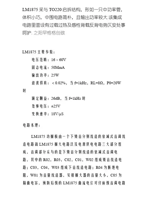
小功率功放电路图如下图所示。
本音频信号放大器主要用于频带为300Hz~3400Hz范围内,它可广泛用于通讯机中的公务联络,也可用于小型音响、收录机、收音机放大,以及其它音频故障接收信号。
工作原理
电路原理如图所示。
本放大器由三极管VT1、VT2、VT3、变压器T1、T2及相关元件组成。
微弱的信号ui由输入变压器T1,感应的信号送到前置放大器VT1的基极进行放大,其集电极将放大信号送到变压器T2,T2的作用能使单端变成双端,则T2的次级绕制的两组分别送至由三极管VT2和VT3组成的单端推换式放大电路,工作于甲乙类状态。
经耦合电容C5、C6送到扬声器BL,BL发出放大后的音频信号。
技术指标:
电源电压- 6 - 12 VDC
输出功放- 1 W, 8 Ohm
采用6V供电时其静态功耗只有24mW
输入-输出配置
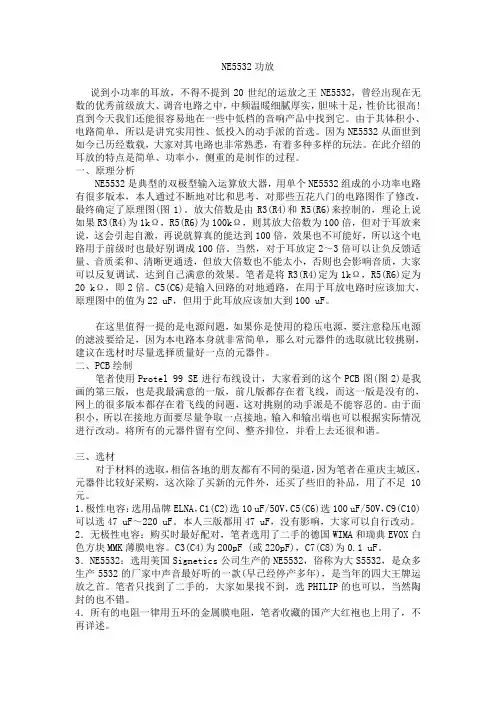
LM386功放电路图:
LM386小功率功放电路报目单:
LM386功放电路PCB图:
TDA2822双声道小功率功放电路图
TDA2822是小功率集成功放,其特点是:工作电压低,低于1.8V时仍能正常工作,集成度高,外围元件少,音质好。
TDA2822广泛应用于收音机、随身听、耳机放大器等小功率功放电路中。
如图1所示为TDA2822用于立体声功放的典型应用电路。
图中,R1,R2是输入偏置电阻,C1,C2是负反馈端的接地电容气,C6,C7是输出耦合电容,R3,C4和R4,C5是高次谐波抑制电路,用于防止电路振荡。
如图2所示为TDA2822用于立体声耳机的应用电路。
图1 TDA2822用于立体声功放的应用电路
图2 TDA2822用于立体声耳机的应用电路
电路原理:
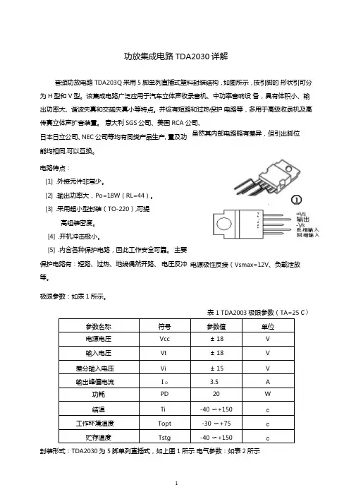
该功放电路如图5-100所示,用了两只TDA2030集成电路做为功率放大;另用一只TL082构成有源伺服电路,TDA2030内部设有过热,过压及输出适中保护,其外围电路元件少,装调十分方便。
有源伺服电路的加入使电路工作更加稳定,同时使失真减至最小。
另外,
元件选择:
小功率音频放大器MC34119电路原理:
迷你音箱:2W放大器电路(Mini-box 2W Amplifier)
双向Parts:
P1 = 10K Log.Potentiometer
R1,R2 = 33K 1/4W Resistors
R3 = 33R 1/4W Resistor
R4 = 15K 1/4W Resistor
R5,R6 = 1K 1/4W Resistors
R7 = 680R 1/4W Resistor
R8 = 120R 1/2W Resistor
R9 = 100R 1/2W Trimmer Cermet
C1,C2 = 10΅F 63V Electrolytic Capacitors
C3 = 100΅F 25V Electrolytic Capacitor
C4,C7 = 470΅F 25V Electrolytic Capacitors
C5 = 47pF 63V Ceramic Capacitor
C6 = 220nF 63V Polyester Capacitor
C8 = 1000΅F 25V Electrolytic Capacitor
D1 = 1N4148 75V 150mA Diode
Q1 = BC560C 45V 100mA PNP Low noise High gain Transistor
Q2 = BC337 45V 800mA NPN Transistor
Q3 = TIP31A 60V 4A NPN Transistor
Q4 = TIP32A 60V 4A PNP Transistor
SW1 SPST switch
SPKR 3-5 Watt Loudspeaker, 8, 4 or 2 Ohm impedance
Device purpose:
This amplifier was designed to be self-contained in a small loudspeaker box. It can be feed by Walkman, Mini-Disc and CD players, computers and similar devices having line or headphone output. Of course, in most cases you'll have to make two boxes to obtain stereo.
The circuit was deliberately designed using no ICs and in a rather old-fashioned manner in order to obtain good harmonic distortion behaviour and to avoid hard to find components. The amplifier(s) can be conveniently supplied by a 12V wall plug-in transformer. Closing SW1 a bass-boost is provided but, at the same time, volume control must be increased to compensate for power loss at higher frequencies.
In use, R9 should be carefully adjusted to provide minimal audible signal cross-over distortion consistent with minimal measured quiescent current consumption; a good compromise is to set the quiescent current at about 10-15 mA.
To measure this current, wire a DC current meter temporarily in series with the collector of Q3.
Technical data:
Output power: 1.5 Watt RMS @ 8 Ohm, 2.5 Watt @ 4 Ohm, 3.5 Watt @ 2 Ohm (1KHz sinewave) Sensitivity: 100mV input for 1.5W output @ 8 Ohm
Frequency response: 30Hz to 20KHz -1dB
Total harmonic distortion @ 1KHz & 10KHz: Below 0.2% @ 8 Ohm 1W, below 0.3% @ 4 Ohm 2W, below 0.5% @ 2 Ohm 2W.。