苏民峰《峰生水起》精读卡全
- 格式:pdf
- 大小:2.51 MB
- 文档页数:6
名著阅读卡模板
一、书名:《XXX》
二、作者:[XXXXX]
三、出版年份:XXXX年
四、主要人物:XXX、XXX、XXX等
五、主题思想:本书通过讲述XXX等人的故事,探讨了XXXXXX主题,表达了XXXXXXX思想。
六、情节概述:本书主要讲述了XXX因为XXXXXX 而踏上了XXXXXX的旅程,期间遭遇了XXXXXX等事件,最终实现了XXXXXX目标。
七、名言佳句:
1. XXXX
2. XXXX
3. XXXX
八、阅读感悟:通过阅读本书,我深入地认识到了XXXXXX,也深刻地感受到了XXX的勇气和决心。
这本书让我思考了XXXXXX问题,对于我的成长和发展有很大的启示。
九、推荐指数:五颗星(最高为五颗星)
十、相关评论:
1. XXXX说:“这是一本非常值得一读的名著。
”
2. XXXX认为:“这本书不仅情节吸引人,更重要的是它传达了一种积极向上的思想。
”。
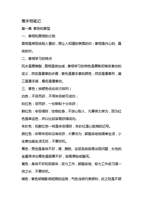
看手相笔记第一集掌色和掌型一、掌相和面相的分别面相是表现给别人看的,想让人知道的表面的你;掌相是内心的、真实的你。
二、掌相学习的特点风水是要推敲,面相是做加减,掌相学习的特色是要熟知每条掌纹的定义,然后是看掌的步骤:首先是看手掌的颜色,然后是看掌形,第三是看手指,最后是看掌纹。
三、掌色(按颜色优劣依次排列)白色:不劳而获,不用辛劳就可成功;粉红色:劳而获,一份耕耘十分收获;鲜红色:辛劳得财,性格较急,不放心别人、凡事亲力亲为,因为红色是幸运色,所以比较容易获得成功。
朱砂色:和鲜红色一样是辛劳得财,朱砂红是心脏病的记号。
瘀红色:非常辛劳却没有收获,大事勿为,脚踏实地地简单生活,小生意也能生活无忧,不要投机。
青色:男性是身体不好,肾、膀胱、泌尿系统容易出现问题,女性的金星带浮出青色是肠胃不好,容易便秘或腹泻。
黄色:身体不好和劳碌命,劳力工作,脚踏实地、努力工作或习得一技之长,不要投机。
暗色:掌色明暗影响短期的运势,气色浅明代表顺利,反之则是不顺利。
四、掌型1.原始型掌:手掌厚、硬、阔、色红(像猩猩的手掌)。
长期从事稳定的工作,表面懦弱怕事,当压力过大时会失去理性,露出凶性。
2.方形掌:手掌、指甲形方,手指粗而整齐,长期从事手工或技术型工作,较实际,实事求是,生活一板一眼,是一个负责人的好丈夫,但生活较少情趣。
3.长方形掌:有活力,懂得享受生活,有生活情趣,喜欢安定的生活。
4.圆形掌:善于把握机会,懂得享受生活,性格多变,意志力不足,容易随波逐流。
手腕圆滑,拇指到达或超过食指第三节时,做事头头是道,容易在恶劣的环境中冲破困难而成功,反之则是则是执行力不足,想事情天下无敌,做起事却无能为力。
五、实践总结左手看30岁以前,右手看30岁以后哦;手掌气色,左手看过去一年,右手看未来一年。
腮骨宽大有力,面相叫“纸老虎”,外表精明强干,内心脆弱。
六、案例1.圆形掌,拇指太短,实行力不足,下巴斜是性格冲动,性格冲动加上决心不足,就是急于做事,但是转头就后悔,无法善后。


DS90LV048A3V LVDS Quad CMOS Differential Line ReceiverGeneral DescriptionThe DS90LV048A is a quad CMOS flow-through differential line receiver designed for applications requiring ultra low power dissipation and high data rates.The device is de-signed to support data rates in excess of 400Mbps (200MHz)utilizing Low Voltage Differential Signaling (LVDS)technology.The DS90LV048A accepts low voltage (350mV typical)dif-ferential input signals and translates them to 3V CMOS out-put levels.The receiver supports a TRI-STATE ®function that may be used to multiplex outputs.The receiver also supports open,shorted and terminated (100Ω)input fail-safe.The re-ceiver output will be HIGH for all fail-safe conditions.The DS90LV048A has a flow-through pinout for easy PCB layout.The EN and EN *inputs are ANDed together and control the TRI-STATE outputs.The enables are common to all four re-ceivers.The DS90LV048A and companion LVDS line driver (eg.DS90LV047A)provide a new alternative to high power PECL/ECL devices for high speed point-to-point interface applications.Featuresn >400Mbps (200MHz)switching ratesn Flow-through pinout simplifies PCB layout n 150ps channel-to-channel skew (typical)n 100ps differential skew (typical)n 2.7ns maximum propagation delay n 3.3V power supply designn High impedance LVDS inputs on power down n Low Power design (40mW 3.3V static)n Interoperable with existing 5V LVDS driversn Accepts small swing (350mV typical)differential signal levelsn Supports open,short and terminated input fail-safe n Conforms to ANSI/TIA/EIA-644Standardn Industrial temperature operating range (-40˚C to +85˚C)nAvailable in SOIC and TSSOP packageConnection DiagramFunctional DiagramENABLESINPUTS OUTPUT EN EN*R IN+−R IN−R OUT HL or OpenV ID ≥0.1V H V ID ≤−0.1V L Full Fail-safe OPEN/SHORT or TerminatedHAll other combinations of ENABLE inputs X ZTRI-STATE ®is a registered trademark of National Semiconductor Corporation.Dual-in-LineDS100888-1Order Number DS90LV048ATM,DS90LV048ATMTCSee NS Package Number M16A,MTC16July 1999DS90LV048A 3V LVDS Quad CMOS Differential Line Receiver©1999National Semiconductor Corporation Absolute Maximum Ratings(Note1)If Military/Aerospace specified devices are required, please contact the National Semiconductor Sales Office/ Distributors for availability and specifications.Supply Voltage(V CC)−0.3V to+4V Input Voltage(R IN+,R IN−)−0.3V to3.9V Enable Input Voltage(EN,EN*)−0.3V to(V CC+0.3V) Output Voltage(R OUT)−0.3V to(V CC+0.3V) Maximum Package Power Dissipation+25˚CM Package1025mW MTC Package866mW Derate M Package8.2mW/˚C above+25˚C Derate MTC Package 6.9mW/˚C above+25˚C Storage Temperature Range−65˚C to+150˚C Lead Temperature Range Soldering(4sec.)+260˚C Maximum Junction Temperature+150˚C ESD Rating(Note10)(HBM,1.5kΩ,100pF)≥10kV (EIAJ,0Ω,200pF)≥1200VRecommended Operating ConditionsMin Typ Max Units Supply Voltage(V CC)+3.0+3.3+3.6V Receiver Input Voltage GND+3.0V Operating Free AirTemperature(T A)−4025+85˚CElectrical CharacteristicsOver Supply Voltage and Operating Temperature ranges,unless otherwise specified.(Notes2,3)Symbol Parameter Conditions Pin Min Typ Max Units V TH Differential Input High Threshold V CM=+1.2V,0.05V,2.95V(Note13)R IN+,+100mV V TL Differential Input Low Threshold R IN−−100mV VCMR Common-Mode Voltage Range VID=200mV pk to pk(Note5)0.1 2.3V I IN Input Current V IN=+2.8V V CC=3.6V or0V−10±5+10µAV IN=0V−10±1+10µAV IN=+3.6V V CC=0V-20±1+20µA V OH Output High Voltage I OH=−0.4mA,V ID=+200mV R OUT 2.7 3.3VI OH=−0.4mA,Input terminated 2.7 3.3VI OH=−0.4mA,Input shorted 2.7 3.3V V OL Output Low Voltage I OL=2mA,V ID=−200mV0.050.25V I OS Output Short Circuit Current Enabled,V OUT=0V(Note11)−15−47−100mA I OZ Output TRI-STATE Current Disabled,V OUT=0V or V CC−10±1+10µAV IH Input High Voltage EN,EN*2.0V CC VV IL Input Low Voltage GND0.8V I I Input Current V IN=0V or V CC,Other Input=V CC orGND−10±5+10µA V CL Input Clamp Voltage I CL=−18mA−1.5−0.8V I CC No Load Supply CurrentReceivers EnabledEN=V CC,Inputs Open V CC915mA I CCZ No Load Supply Current EN=GND,Inputs Open15mAReceivers DisabledSwitching CharacteristicsOver Supply Voltage and Operating Temperature ranges,unless otherwise specified.(Notes3,4,7,8)Symbol Parameter Conditions Min Typ Max Units t PHLD Differential Propagation Delay High to Low C L=15pF 1.2 2.0 2.7ns t PLHD Differential Propagation Delay Low to High V ID=200mV 1.2 1.9 2.7ns t SKD1Differential Pulse Skew|t PHLD−t PLHD|(Note6)(Figure1and Figure2)00.10.4ns t SKD2Differential Channel-to-Channel Skew;same device(Note7)00.150.5ns t SKD3Differential Part to Part Skew(Note8) 1.0ns t SKD4Differential Part to Part Skew(Note9) 1.5ns t TLH Rise Time0.5 1.0ns t THL Fall Time0.35 1.0ns 2Switching Characteristics(Continued)Over Supply Voltage and Operating Temperature ranges,unless otherwise specified.(Notes3,4,7,8)Symbol Parameter Conditions Min Typ Max Units t PHZ Disable Time High to Z R L=2kΩ814nst PLZ Disable Time Low to Z C L=15pF814nst PZH Enable Time Z to High(Figure3and Figure4)914nst PZL Enable Time Z to Low914nsf MAX Maximum Operating Frequency(Note14)All Channels Switching200250MHzNote1:“Absolute Maximum Ratings”are those values beyond which the safety of the device cannot be guaranteed.They are not meant to imply that the devices should be operated at these limits.The table of“Electrical Characteristics”specifies conditions of device operation.Note2:Current into device pins is defined as positive.Current out of device pins is defined as negative.All voltages are referenced to ground unless otherwise speci-fied.Note3:All typicals are given for:V CC=+3.3V,T A=+25˚C.Note4:Generator waveform for all tests unless otherwise specified:f=1MHz,Z O=50Ω,t r and t f(0%to100%)≤3ns for R IN.Note5:The VCMR range is reduced for larger VID.Example:if VID=400mV,the VCMR is0.2V to2.2V.The fail-safe condition with inputs shorted is not supported over the common-mode range of0V to2.4V,but is supported only with inputs shorted and no external common-mode voltage applied.A VID up to V CC−0V may be applied to the R IN+/R IN−inputs with the Common-Mode voltage set to V CC/2.Propagation delay and Differential Pulse skew decrease when VID is increased from 200mV to400mV.Skew specifications apply for200mV≤VID≤800mV over the common-mode range.Note6:t SKD1is the magnitude difference in differential propagation delay time between the positive going edge and the negative going edge of the same channel Note7:t SKD2,Channel-to-Channel Skew is defined as the difference between the propagation delay of one channel and that of the others on the same chip with any event on the inputs.Note8:t SKD3,part to part skew,is the differential channel-to-channel skew of any event between devices.This specification applies to devices at the same V CC, and within5˚C of each other within the operating temperature range.Note9:t SKD4,part to part skew,is the differential channel-to-channel skew of any event between devices.This specification applies to devices over recommended operating temperature and voltage ranges,and across process distribution.t SKD4is defined as|Max−Min|differential propagation delay.Note10:ESD Rating:HBM(1.5kΩ,100pF)≥10kVEIAJ(0Ω,200pF)≥1200VNote11:Output short circuit current(I OS)is specified as magnitude only,minus sign indicates direction only.Only one output should be shorted at a time,do not exceed maximum junction temperature specification.Note12:C L includes probe and jig capacitance.Note13:V CC is always higher than R IN+and R IN−voltage.R IN−and R IN+are allowed to have a voltage range−0.2V to V CC−VID/2.However,to be compliant with AC specifications,the common voltage range is0.1V to2.3VNote14:f MAX generator input conditions:t r=t f<1ns(0%to100%),50%duty cycle,differential(1.05V to1.35V peak to peak).Output criteria:60/40%duty cycle, V OL(max0.4V),V OH(min2.7V),Load=15pF(stray plus probes).Parameter Measurement InformationDS100888-3FIGURE1.Receiver Propagation Delay and Transition Time Test CircuitDS100888-4FIGURE2.Receiver Propagation Delay and Transition Time Waveforms3Parameter Measurement Information(Continued)Typical ApplicationApplications InformationGeneral application guidelines and hints for LVDS drivers and receivers may be found in the following application notes:LVDS Owner’s Manual (lit #550062-001),AN808,AN977,AN971,AN916,AN805,AN903.LVDS drivers and receivers are intended to be primarily used in an uncomplicated point-to-point configuration as is shown in Figure 5.This configuration provides a clean signaling en-vironment for the fast edge rates of the drivers.The receiver is connected to the driver through a balanced media which may be a standard twisted pair cable,a parallel pair cable,or simply PCB traces.Typically,the characteristic impedance ofthe media is in the range of 100Ω.A termination resistor of 100Ω(selected to match the media),and is located as close to the receiver input pins as possible.The termination resis-tor converts the driver output (current mode)into a voltage that is detected by the receiver.Other configurations are possible such as a multi-receiver configuration,but the ef-fects of a mid-stream connector(s),cable stub(s),and other impedance discontinuities as well as ground shifting,noise margin limits,and total termination loading must be taken into account.DS100888-5C L includes load and test jig capacitance.S 1=V CC for t PZL and t PLZ measurements.S 1=GND for t PZH and t PHZ measurements.FIGURE 3.Receiver TRI-STATE Delay Test CircuitDS100888-6FIGURE 4.Receiver TRI-STATE Delay WaveformsBalanced SystemDS100888-7FIGURE 5.Point-to-Point Application4Applications Information(Continued)The DS90LV048A differential line receiver is capable of de-tecting signals as low as100mV,over a±1V common-mode range centered around+1.2V.This is related to the driver off-set voltage which is typically+1.2V.The driven signal is cen-tered around this voltage and may shift±1V around this cen-ter point.The±1V shifting may be the result of a ground potential difference between the driver’s ground referenceand the receiver’s ground reference,the common-mode ef-fects of coupled noise,or a combination of the two.The ACparameters of both receiver input pins are optimized for arecommended operating input voltage range of0V to+2.4V(measured from each pin to ground).The device will operatefor receiver input voltages up to V CC,but exceeding V CC willturn on the ESD protection circuitry which will clamp the busvoltages.The DS90LV048A has a flow-through pinout that allows foreasy PCB layout.The LVDS signals on one side of the de-vice easily allows for matching electrical lengths of the differ-ential pair trace lines between the driver and the receiver aswell as allowing the trace lines to be close together to couplenoise as common-mode.Noise isolation is achieved with theLVDS signals on one side of the device and the TTL signalson the other side.Power Decoupling Recommendations:Bypass capacitors must be used on power e highfrequency ceramic(surface mount is recommended)0.1µFand0.001µF capacitors in parallel at the power supply pinwith the smallest value capacitor closest to the device supplypin.Additional scattered capacitors over the printed circuitboard will improve decoupling.Multiple vias should be usedto connect the decoupling capacitors to the power planes.A10µF(35V)or greater solid tantalum capacitor should beconnected at the power entry point on the printed circuitboard between the supply and ground.PC Board considerations:Use at least4PCB layers(top to bottom);LVDS signals,ground,power,TTL signals.Isolate TTL signals from LVDS signals,otherwise the TTLmay couple onto the LVDS lines.It is best to put TTL andLVDS signals on different layers which are isolated by apower/ground plane(s)Keep drivers and receivers as close to the(LVDS port side)connectors as possible.Differential Traces:Use controlled impedance traces which match the differen-tial impedance of your transmission medium(ie.cable)andtermination resistor.Run the differential pair trace lines asclose together as possible as soon as they leave the IC(stubs should be<10mm long).This will help eliminate re-flections and ensure noise is coupled as common-mode.Infact,we have seen that differential signals which are1mmapart radiate far less noise than traces3mm apart sincemagnetic field cancellation is much better with the closertraces.In addition,noise induced on the differential lines ismuch more likely to appear as common-mode which is re-jected by the receiver.Match electrical lengths between traces to reduce skew.Skew between the signals of a pair means a phase differ-ence between signals which destroys the magnetic field can-cellation benefits of differential signals and EMI will result.(Note the velocity of propagation,v=c/Er where c(thespeed of light)=0.2997mm/ps or0.0118in/ps).Do not relysolely on the autoroute function for differential traces.Care-fully review dimensions to match differential impedance andprovide isolation for the differential lines.Minimize the num-ber or vias and other discontinuities on the line.Avoid90˚turns(these cause impedance discontinuities).Use arcs or45˚bevels.Within a pair of traces,the distance between the two tracesshould be minimized to maintain common-mode rejection ofthe receivers.On the printed circuit board,this distanceshould remain constant to avoid discontinuities in differentialimpedance.Minor violations at connection points are allow-able.Termination:Use a termination resistor which best matches the differen-tial impedance or your transmission line.The resistor shouldbe between90Ωand130Ω.Remember that the currentmode outputs need the termination resistor to generate thedifferential voltage.LVDS will not work without resistor termi-nation.Typically,connecting a single resistor across the pairat the receiver end will suffice.Surface mount1%to2%resistors are best.PCB stubs,component lead,and the distance from the termination to thereceiver inputs should be minimized.The distance betweenthe termination resistor and the receiver should be<10mm(12mm MAX)Probing LVDS Transmission Lines:Always use high impedance(>100kΩ),lowcapacitance(<2pF)scope probes with a wide bandwidth(1GHz)scope.Improper probing will give deceiving results.Cables and Connectors,General Comments:When choosing cable and connectors for LVDS it is impor-tant to remember:Use controlled impedance media.The cables and connec-tors you use should have a matched differential impedanceof about100Ω.They should not introduce major impedancediscontinuities.Balanced cables(e.g.twisted pair)are usually better thanunbalanced cables(ribbon cable,simple coax.)for noise re-duction and signal quality.Balanced cables tend to generateless EMI due to field canceling effects and also tend to pickup electromagnetic radiation a common-mode(not differen-tial mode)noise which is rejected by the receiver.For cable distances<0.5M,most cables can be made towork effectively.For distances0.5M≤d≤10M,CAT3(cat-egory3)twisted pair cable works well,is readily availableand relatively inexpensive.Fail-Safe Feature:The LVDS receiver is a high gain,high speed device thatamplifies a small differential signal(20mV)to CMOS logiclevels.Due to the high gain and tight threshold of the re-ceiver,care should be taken to prevent noise from appearingas a valid signal.The receiver’s internal fail-safe circuitry is designed tosource/sink a small amount of current,providing fail-safeprotection(a stable known state of HIGH output voltage)forfloating,terminated or shorted receiver inputs.1.Open Input Pins.The DS90LV048A is a quad receiverdevice,and if an application requires only1,2or3re-ceivers,the unused channel(s)inputs should be leftOPEN.Do not tie unused receiver inputs to ground orany other voltages.The input is biased by internal highvalue pull up and pull down resistors to set the output toa HIGH state.This internal circuitry will guarantee aHIGH,stable output state for open inputs. 5Applications Information(Continued)2.Terminated Input.If the driver is disconnected (cable unplugged),or if the driver is in a TRI-STATE or power-off condition,the receiver output will again be in a HIGH state,even with the end of cable 100Ωtermination resis-tor across the input pins.The unplugged cable can be-come a floating antenna which can pick up noise.If the cable picks up more than 10mV of differential noise,the receiver may see the noise as a valid signal and switch.To insure that any noise is seen as common-mode and not differential,a balanced interconnect should be used.Twisted pair cable will offer better balance than flat rib-bon cable.3.Shorted Inputs.If a fault condition occurs that shortsthe receiver inputs together,thus resulting in a 0V differ-ential input voltage,the receiver output will remain in a HIGH state.Shorted input fail-safe is not supported across the common-mode range of the device (GND to 2.4V).It is only supported with inputs shorted and no ex-ternal common-mode voltage applied.External lower value pull up and pull down resistors (for a stronger bias)may be used to boost fail-safe in the presence of higher noise levels.The pull up and pull down resistors should be in the 5k Ωto 15k Ωrange to minimize loading and waveform distortion to the driver.The common-mode bias point should be set to approximately 1.2V (less than 1.75V)to be compatible with the internal circuitry.Pin DescriptionsPin Description2,3,6,7R IN+Non-inverting receiver input pin 1,4,5,8R IN−Inverting receiver input pin 10,11,14,R OUTReceiver output pin1516ENReceiver enable pin:When EN is low,the receiver is disabled.When EN is high and EN*is low or open,the receiver is enabled.If both EN and EN*are open circuit,then the receiver is disabled.9EN*Receiver enable pin:When EN*is high,the receiver is disabled.When EN*is low or open and EN is high,the receiver isenabled.If both EN and EN*are open circuit,then the receiver is disabled.13V CC Power supply pin,+3.3V ±0.3V 12GNDGround pinOrdering InformationOperating Package Type/Order NumberTemperature Number −40˚C to +85˚C SOP/M16A DS90LV048ATM −40˚C to +85˚CTSSOP/MTC16DS90LV048ATMTC Typical Performance CurvesOutput High Voltage vs Power Supply VoltageDS100888-12Output Low Voltage vs Power Supply VoltageDS100888-13 6Typical Performance Curves(Continued)Output Short Circuit Current vsPower Supply VoltageDS100888-14Output TRI-STATE Current vsPower Supply VoltageDS100888-15Differential Transition Voltage vsPower Supply VoltageDS100888-16Power Supply Currentvs FrequencyDS100888-17Power Supply Current vsAmbient TemperatureDS100888-18Differential Propagation Delay vsPower Supply VoltageDS100888-19 7Typical Performance Curves(Continued)Differential Propagation Delay vs Ambient TemperatureDS100888-20Differential Propagation Delay vs Differential Input VoltageDS100888-21Differential Propagation Delay vs Common-Mode Voltage DS100888-22Differential Skew vs Power Supply VoltageDS100888-23Differential Skew vs Ambient Temperature DS100888-24Transition Time vs Power Supply VoltageDS100888-25 8Typical Performance Curves(Continued)Transition Time vsAmbient TemperatureDS100888-269Physical Dimensions inches(millimeters)unless otherwise noted16-Lead(0.150"Wide)Molded Small Outline Package,JEDECOrder Number DS90LV048ATMNS Package Number M16A10Physical Dimensions inches(millimeters)unless otherwise noted(Continued)LIFE SUPPORT POLICYNATIONAL’S PRODUCTS ARE NOT AUTHORIZED FOR USE AS CRITICAL COMPONENTS IN LIFE SUPPORT DEVICES OR SYSTEMS WITHOUT THE EXPRESS WRITTEN APPROVAL OF THE PRESIDENT AND GENERAL COUNSEL OF NATIONAL SEMICONDUCTOR CORPORATION.As used herein:1.Life support devices or systems are devices orsystems which,(a)are intended for surgical implantinto the body,or(b)support or sustain life,andwhose failure to perform when properly used inaccordance with instructions for use provided in thelabeling,can be reasonably expected to result in asignificant injury to the user.2.A critical component is any component of a lifesupport device or system whose failure to performcan be reasonably expected to cause the failure ofthe life support device or system,or to affect itssafety or effectiveness.National SemiconductorCorporationAmericasTel:1-800-272-9959Fax:1-800-737-7018Email:support@National SemiconductorEuropeFax:+49(0)180-5308586Email:europe.support@Deutsch Tel:+49(0)180-5308585English Tel:+49(0)180-5327832Français Tel:+49(0)180-5329358Italiano Tel:+49(0)180-5341680National SemiconductorAsia Pacific CustomerResponse GroupTel:65-2544466Fax:65-2504466Email:sea.support@National SemiconductorJapan Ltd.Tel:81-3-5639-7560Fax:81-3-5639-7507 16-Lead(0.100"Wide)Molded Thin Shrink Small Outline Package,JEDECOrder Number DS90LV048ATMTCNS Package Number MTC16DS90LV048A3VLVDSQuadCMOSDifferentialLineReceiver National does not assume any responsibility for use of any circuitry described,no circuit patent licenses are implied and National reserves the right at any time without notice to change said circuitry and specifications.。

一本到位名著精读精练
一本到位名著精读精练,是指通过对名著的深入阅读和精心练习,达到对其内容和精华的全面理解和掌握。
名著是指在文学、哲学、历史和社会等领域中,具有深远影响和不朽价值的作品。
在进行名著精读精练时,需要注意以下几点:
1.全面了解名著的背景和作者的生平,了解其写作背景和社会背景,有助于深入理解作品的内涵和价值。
2.注重文本分析和理解,深入思考作品中的情节、人物、主题等要素,挖掘其深层次的含义。
3.注重练习,通过写作、讲解、复述等方式,深化对作品的理解和掌握,让自己在实践中不断提高。
4.注重与他人的交流和讨论,通过与他人的沟通和交流,了解不同的观点和解读方式,进一步加深对作品的理解。
在名著精读精练的过程中,需要注意的是,不要被作品的表面现象所迷惑,要深入挖掘作品背后的思想和内涵,从而真正理解和掌握作品的精华。
同时,要注意遵循个人兴趣和能力的发展方向,选择适合自己的名著进行精读精练。
总之,名著精读精练是提高自身素养和文化水平的重要途径,通过深入理解和掌握名著的内容和精华,不仅能够提高个人的思维能力和品味,也能够为个人的成长和发展打下坚实的基础。
- 1 -。
男命女命岁运男命2330洞门无锁钥闺门深似海半空明月稀2441雪浪震天鼓便是一闲人应不染红尘一枕清风静扁舟在下行2331月在清波底年来十二月酒醒何处去2542掌中秋月扇维舟向柳边月长日西沉柳岸晚风轻举动好风生2332商山秦岭花花果一时新商山採药去2643流转运元气开向三冬雪回首四面隔意望作神仙阴阳有准绳2744两羊排山崖披烟看钩栈2845登山延木设桃吐落阳花2433元宵好灯烛紫燕语离情将军预断桥3340一点浮云翳却向五更明新巢重引子谋为何计策鸿羽逐风飞2534三年不言道牛女星方度梅花雪下开2241舟放浪波翻梦传说旁求谁家度浪生巳自压群芳洞庭风送雁2635观鼎取其象花上莺声急苍鹰与良犬2342华亭鸣鹤唳稼穑下艰难东风叹短长须日渐从游云月出西山2736结绳代书契革故取鼎新骏马已登途2443琴上挂田租八卦未曾成婚姻事非偶阻防蹄暂住移人于河东2837华渚星虹动罗帐怕霜侵凤鸣在高岗2544虎兕出于押海棠云雨飞云外衣裳冷百鸟皆集视征夫不能行2938鸿毛飞白雪惟愿日长好用扇作飞帘2645轩辂飏清风羊角上清霄旬西还自东粪尘如风卷虚心皆自贯3039鱼虾北海过葛藟系穋木凿井得逢泉2746乘舟渡日月海水变桑田前程自由期先劳而后畅天表厌烟波2140惟鱼与熊掌清沟自澄清生义人所欲3342岩畔青松树二者岂能兼莫使决污泥二者岂能兼根磐石上生2241虎皮包干戈江天欲暮时蝴蝶上天飞2243金波浸明月华山未归马惆怅神仙侣寻花去上苑雷电捧天星【注解】商山:山名,在今陕西商县东,相传秦末汉初东园公、绮里季、夏黄公、甪里四人曾隐居商山,这里亦含隐士之意。
本节标题所谓 “新补”者,原书既题“宋华山希夷先生陈抟著、康节尧夫先生雍述,明覃怀史应选念冲甫校订”,“新补”则当为明念翁所为;以下四部原标题均无“新补”二字,当为漏刻。
3332自牖看天心春分酒一壶雪满芳郊外2344蜂酿百花酒咫尺天颜近明月人千里此心惟是忧其甘与世殊2233月出四更静要知天不晓定前须向日长天雁字横月色转三更何在更登楼2334海裳三月开梅子坠金凤马过危桥上雨洗胭脂脸不见钗头凤提防脚下空2445竹花开石上2435白露结珠花明珠生老蚌OOOOO结果不生笋东边太阳上莫戏绿杨津OOOOO2546点火八九渊2536绣针为铁柱铁磐与铜盒得薪又无米匮中有龟玉江海暗中灜相刚方稳当恍惚又忧惶2647寸阴惟我惜2637二气包鳌极天边问明月夜深闻雷声稼穑为君爱五行犹未分已度又还圆疑有所思时3344泰宇清明地2738花笺黑水染仙曲何人和扁舟兼得舫无言独履霜空有五云飞玉箫吹夜寒向后飞出常2245云电斗星见2839赤电闪红旗月中丹桂子蛇蟠当道上石路马蹄轻黑云拖铁骑开处待秋风进退自为忧2346北斗日中见2940巫山千里远郑北春风生禽蟹脕云谷斯言传古今欲听鸟声音霜雪摧蒲柳振羽欲飞时2447初生嫩松柏3041龙舟争胜负东风蒲柳花画舫过洪波栽向雪霜中欲定一时名西风何太急棹短难得渡2548惟我有用禾3142樲棘共梧檟鲍鱼混芝兰桂林无雨露一井供万灶取养在场师馨香依旧在山泽有风云3346芧屋蒿供祭3334物均衡斗正杨朱恶修身闹吏听驻笛百神皆享之益寡亦裒多难遇天仙子躁进恐无由2247烟霞朝日食吾道不雷同2348去敲天上鼓跣足履冰霜2449红添绿减处2235龙蛇争一室云开月色新猛虎居林丛鸟啼三月天飞向百花丛阴晴犹未保笑吼自生风3348丘陵势自殊【注解】樲;音二,古指酸枣树。
封面
这是封面的内容,包括书名、作者、出版社、出版日期等信息。
目录
以下是本书的目录:
1.第一章 1.1 节标题 1.1.1 子节标题 1.1.2 子节标题 1.2 节标题
1.2.1 子节标题 1.2.2 子节标题
2.第二章 2.1 节标题 2.1.1 子节标题 2.1.2 子节标题 2.2 节标题
2.2.1 子节标题 2.2.2 子节标题
3.第三章 3.1 节标题 3.1.1 子节标题 3.1.2 子节标题 3.2 节标题
3.2.1 子节标题 3.2.2 子节标题
前言
在工作和生活中,我们经常会遇到各种问题和挑战,面对复杂多变的情况,我们需要不断学习和提升自己的能力,以应对未来的挑战。
本书旨在通过对一些实际问题的分析和解决方法的介绍,帮助读者了解和掌握相关知识和技能,提高工作和生活的质量。
本书内容主要包括以下几个方面:
1.xxx
2.xxx
3.xxx
在本书写作过程中,我们充分参考了相关的资料和文献,并借鉴了一些成功案例和经验,同时还请了一些专家和从业者进行了专业性的讲解和评价,以保证本书的准确性和实用性。
最后,我们真诚地感谢所有对本书写作和出版做出贡献的人员和机构,希望本书能够为读者提供实用的帮助和指导。
自然科学普及读物有机高分子材料集萃向海洋要淡水现代社会的水危机水是人类赖以生存的基本物质。
人可以7~10天不进食,却不能不饮水。
要知道,人体总重量的70%是水,血液中的含水量更高,达83%。
世界各国的工业化给人类带来了物质文明,但也产生了负面影响。
人是人类社会最宝贵的财富,但人口的猛增也给地球带来了沉重的负担。
就拿水来说,由于工业的发展和人口的猛增,地球已发生了水危机。
早在1972年,联合国在瑞典斯德哥尔摩召开人类环境会议,许多国家的代表在会上都提到城市缺水和水严重污染的问题。
会议纪要中也写道:“遍及世界的许多地区,由于工业膨胀和每人消费量的提高,需水量已增加到超过天然来源的境地……”如果我们乘坐在宇宙飞船上,居高临下看地球,就可以看到:西欧最大的河流——全长1320千米的莱茵河,由于沿岸各国污染物的排入,已成了“欧洲最大的下水道”,河水变成红褐色,鱼类大量死亡;美国号称“百川之父”的密西西比河,其流域面积达美国大陆的1/4,也处于危机之中;被俄罗斯人称为“母亲河”的伏尔加河,几乎接受了该国一半的污水。
再看看发展中国家,我们也无法乐观:南美洲拥有的世界第一长度和第一大水量的亚马孙河被污染着;被印度人敬为“圣河”的恒河,曾因受污染而导致几万人患黄疸病,许多人因此死亡。
人口的急增是水危机的又一重大原因。
据科学家测算,每人每天约需饮用清洁水5升,加上其他生活用水,共需几百升。
1830年世界人口是10亿,1930年增加到20亿,1960年达到30亿,1975年已有40亿,1990年高达53亿,预计到2000年世界人口至少达63亿。
而据世界卫生组织的调查,早在70年代中期,世界上就已有70%的人得不到安全、卫生的水了。
如此算来,很快就会有90%以上的人饮用不到安全、卫生的水。
到那时,说“水贵如油”毫不过分。
根本的出路:海水淡化让我们还是在宇宙飞船上往下看,你会看到:地球表面的70.8%被水覆盖着,总水量达13.56亿立方千米。