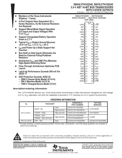
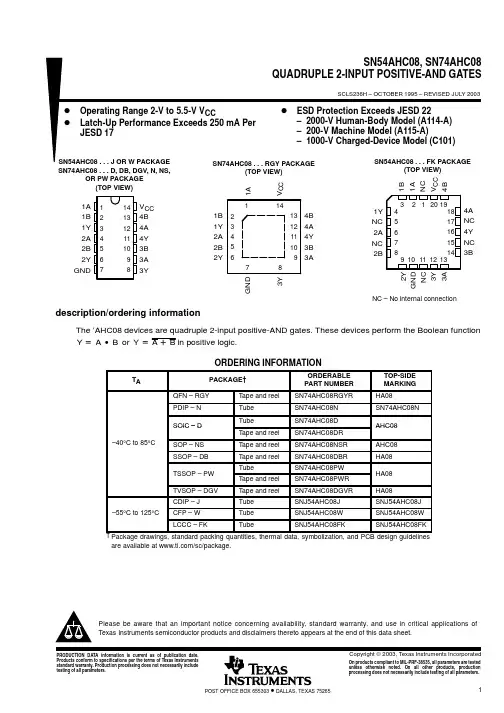
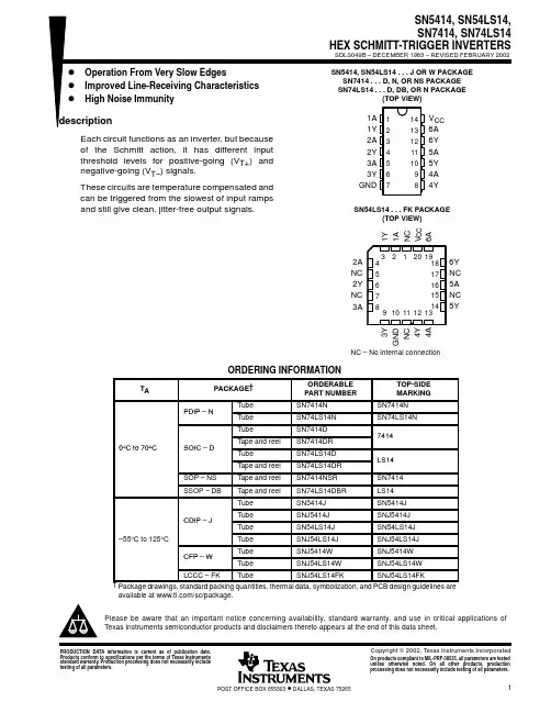
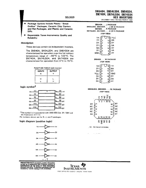
SNJ54LVCH244AW中文资料
- 格式:pdf
- 大小:642.38 KB
- 文档页数:23
TA –40°C to 85°C –55°C to 125°C
ORDERING INFORMATION
PACKAGE (1)
ORDERABLE PART NUMBER
QFN – RGY
Reel of 1000
SN74LVCH244ARGYR
SOIC – DW
Tube of 25 Reel of 2000
• Operate From 1.65 V to 3.6 V
• Inputs Accept Voltages to 5.5 V
• Max tpd of 5.9 ns at 3.3 V • Typical VOLP (Output Ground Bounce)
<0.8 V at VCC = 3.3 V, TA = 25°C • Typical VOHV (Output VOH Undershoot)
元器件交易网
SN54LVCH244A, SN74LVCH244A OCTAL BUFFERS/DRIVERS WITH 3-STATE OUTPUTS
SCES009O – JULY 1995 – REVISED FEBRUARY 2007
FEATURES
These devices are organized as two 4-bit line drivers with separate output-enable (OE) inputs. When OE is low, these devices pass data from the A inputs to the Y outputs. When OE is high, the outputs are in the high-impedance state.
Active bus-hold circuitry holds unused or undriven inputs at a valid logic state. Use of pullup or pulldown resistors with the bus-hold circuitry is not recommended.
Tube of 85
SNJ54LVCH244AW
LCCC – FK
Tube of 55
SNJ54LVCH244AFK
TOP-SIDE MARKING LCH244A
LVCH244A
LVCH244A LCH244A LVCH244A
LCH244A
LCH244A SNJ54LVCH244AJ SNJ54LVCH244AW SNJ54LVCH244AFK
SN74LVCH244APW
TSSOP – PW
Reel of 2000
SN74LVCH244APWR
Reel of 250
SN74LVCH244APWT
TVSOP – DGV
Reel of 2000
SN74LVCH244ADGVR
CDIP – J
Tube of 20
SNJ54LVCH244AJ
CFP – W
Please be aware that an important notice concerning availability, standard warranty, and use in critical applications of Texas Instruments semiconductor products and disclaimers thereto appears at the end of this data sheet.
20 VCC 19 2OE 18 1Y1 17 2A4 16 1Y2 15 2A3 14 1Y3 13 2A2 12 1Y4 11 2A1
1 1A1 2 2Y4 3 1A2 4 2Y3 5 1A3 6 2Y2 7 1A4 8 2Y1 9
10
20 19 2OE 18 1Y1 17 2A4 16 1Y2 15 2A3 14 1Y3 13 2A2 12 1Y4
SN74LVCH244A . . . RGY PACKAGE (TOP VIEW)
SN54LVCH244A . . . FK PACKAGE (TOP VIEW)
2Y4 1A1 1OE VCC 2OE
1OE VCC
1OE 1 1A1 2 2Y4 3 1A2 4 2Y3 5 1A3 6 2Y2 7 1A4 8 2Y1 9 GND 10
Inputs can be driven from either 3.3-V or 5-V devices. This feature allows the use of these devices as translators in a mixed 3.3-V/5-V system environment.
112Y1 GND 2A1Fra bibliotek1Y4 2A2
3 2 1 20 19
1A2 4
18 1Y1
2Y3 5
17 2A4
1A3 6
16 1Y2
2Y2 7
15 2A3
1A4 8
14 1Y3
9 10 11 12 13
GND 2A1
DESCRIPTION/ORDERING INFORMATION
The SN54LVCH244A octal buffer/line driver is designed for 2.7-V to 3.6-V VCC operation, and the SN74LVCH244A octal buffer/line driver is designed for 1.65-V to 3.6-V VCC operation.
– 200-V Machine Model (A115-A)
– 1000-V Charged-Device Model (C101)
SN54LVCH244A . . . J OR W PACKAGE SN74LVCH244A . . . DB, DBQ, DGV, DW,
NS, OR PW PACKAGE (TOP VIEW)
To ensure the high-impedance state during power up or power down, OE should be tied to VCC through a pullup resistor; the minimum value of the resistor is determined by the current-sinking capability of the driver.
3 2Y4
2
Submit Documentation Feedback
元器件交易网
SN54LVCH244A, SN74LVCH244A OCTAL BUFFERS/DRIVERS WITH 3-STATE OUTPUTS
SCES009O – JULY 1995 – REVISED FEBRUARY 2007
These devices are fully specified for partial-power-down applications using Ioff. The Ioff circuitry disables the outputs, preventing damaging current backflow through the devices when they are powered down.
Absolute Maximum Ratings(1)
over operating free-air temperature range (unless otherwise noted)
VCC Supply voltage range
VI
Input voltage range(2)
VO
Voltage range applied to any output in the high-impedance or power-off state(2)
>2 V at VCC = 3.3 V, TA = 25°C • Support Mixed-Mode Signal Operation on All
Ports (5-V Input/Output Voltage With 3.3-V VCC)
• Ioff Supports Partial-Power-Down Mode Operation
INPUTS
OE
A
L
H
L
L
H
X
OUTPUT Y
H L Z
1 1OE
LOGIC DIAGRAM (POSITIVE LOGIC)
19 2OE
2 1A1
18 1Y1
11 2A1
9 2Y1
1A2 4
16 1Y2
2A2 13
7 2Y2
1A3 6
14 1Y3
2A3 15
5 2Y3
1A4 8
12 1Y4
2A4 17
Continuous current through VCC or GND
DB package(4)
DBQ package(4)
DGV package(4)
θJA Package thermal impedance
DW package(4) NS package(4)
PW package(4)
RGY package(5)
Copyright © 1995–2007, Texas Instruments Incorporated
元器件交易网
SN54LVCH244A, SN74LVCH244A OCTAL BUFFERS/DRIVERS WITH 3-STATE OUTPUTS