BSS119GEG中文资料
- 格式:pdf
- 大小:91.89 KB
- 文档页数:8
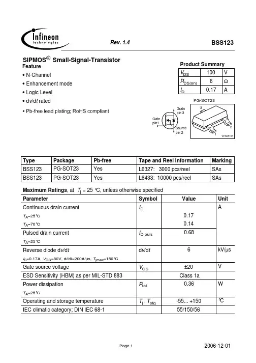
SIPMOS Small-Signal-TransistorProduct SummaryV DS100V R DS(on)6ΩI D0.17AFeature • N-Channel• Enhancement mode • Logic Level• d v /d tratedPG-SOT23123VPS05161Marking sSHType Package Pb-free Tape and Reel Information BSS119PG-SOT23YesL6327: 3000 pcs/reelMaximum Ratings , at T j = 25 °C, unless otherwise specified ParameterSymbol Value Unit Continuous drain currentT A =25°C T A =70°CI D0.170.13APulsed drain currentT A =25°CI D puls0.68Reverse diode d v /d tI S =0.17A, V DS =80V, d i /d t =200A/µs, T jmax =150°Cd v /d t 6kV/µs Gate source voltage V GS ±20V Power dissipationT A =25°CP tot0.36W Operating and storage temperature T j , T stg-55... +150°CIEC climatic category; DIN IEC 68-155/150/56Thermal CharacteristicsParameter Symbol Values Unitmin.typ.max. CharacteristicsThermal resistance, junction - ambientat minimal footprintR thJS--350K/WElectrical Characteristics, at T j = 25 °C, unless otherwise specifiedParameter Symbol Values Unitmin.typ.max. Static CharacteristicsDrain-source breakdown voltageV GS=0, I D=250µAV(BR)DSS100--V Gate threshold voltage, V GS = V DSI D=50µAV GS(th) 1.3 1.8 2.3Zero gate voltage drain current V DS=100V, V GS=0, T j=25°CV DS=100V, V GS=0, T j=150°C I DSS--0.050.50.15µAGate-source leakage currentV GS=20V, V DS=0I GSS-10100nA Drain-source on-state resistanceV GS=4.5V, I D=0.13 AR DS(on)- 4.910ΩDrain-source on-state resistanceV GS=10V, I D=0.17AR DS(on)- 3.46Electrical Characteristics, at T j = 25 °C, unless otherwise specifiedParameter Symbol Conditions Values Unitmin.typ.max. Dynamic CharacteristicsTransconductance g fs V DS≥2*I D*R DS(on)max,I D=0.13A0.080.17-SInput capacitance C iss V GS=0, V DS=25V,f=1MHz -6078pFOutput capacitance C oss-8.611.2 Reverse transfer capacitance C rss- 3.1 4.1Turn-on delay time t d(on)V DD=50V, V GS=10V,I D=0.17A, R G=6Ω- 2.74nsRise time t r- 3.1 4.6Turn-off delay time t d(off)-9.314Fall time t f-2740Gate Charge CharacteristicsGate to source charge Q gs V DD=80V, I D=0.17A-0.080.12nC Gate to drain charge Q gd-0.76 1.1Gate charge total Q g V DD=80V, I D=0.17A,V GS=0 to 10V- 1.67 2.5Gate plateau voltage V(plateau)V DD=80V, I D = 0.17 A - 3.4-V Reverse DiodeInverse diode continuousforward currentI S T A=25°C--0.17AInv. diode direct current, pulsed I SM--0.68 Inverse diode forward voltage V SD V GS=0, I F = I S-0.8 1.2VReverse recovery time t rr V R=50V, I F=l S,d i F/d t=100A/µs -21.732.5nsReverse recovery charge Q rr-1015nC1 Power dissipation P tot = f (T A)BSS119Ptot2 Drain currentI D = f (T A)parameter: V GS≥ 10 VBSS119ID3 Safe operating areaI D = f ( V DS )parameter : D = 0 , T= 25 °C3ID4 Transient thermal impedanceZ thJA = f (t p)parameter : D = t p/T101010101010310K/WBSS119ZthJA5 Typ. output characteristicI D = f (V DS)parameter: T j = 25 °C, V GSID6 Typ. drain-source on resistanceR DS(on) = f (I D)parameter: T j = 25 °C,V GSRDS(on)7 Typ. transfer characteristicsI D= f ( V GS ); V DS≥ 2 x I D x R DS(on)maxparameter: T j = 25 °CID8 Typ. forward transconductanceg fs = f(I D)parameter: T j = 25 °Cgfs9 Drain-source on-state resistance R DS(on) = f (T j )parameter : I D = 0.17 A, VGS = 10 VBSS119R D S (o n )10 Typ. gate threshold voltage VGS(th) = f (T j )parameter: V GS = V DS ; I D=50µAV G S (th )11 Typ. capacitances C = f (V DS )parameter: V GS =0, f =1 MHz, T j = 25 °CC12 Forward character. of reverse diode I F = f (V SD )parameter: TI F13 Typ. gate chargeV GS = f (Q G ); parameter: V DS ,I D = 0.17 A pulsed, T j= 25 °CBSS119V G S14 Drain-source breakdown voltageV (BR)DSS = f (T j)BSS119V (B R )D S SPublished byInfineon Technologies AG,Bereichs KommunikationSt.-Martin-Strasse 53,D-81541 München© Infineon Technologies AG 1999All Rights Reserved.Attention please!The information herein is given to describe certain components and shall not be considered as warranted characteristics.Terms of delivery and rights to technical change reserved.We hereby disclaim any and all warranties, including but not limited to warranties of non-infringement, regarding circuits, descriptions and charts stated herein.Infineon Technologies is an approved CECC manufacturer.InformationFor further information on technology, delivery terms and conditions and prices please contact your nearest Infineon Technologies Office in Germany or our Infineon Technologies Reprensatives worldwide (see address list). WarningsDue to technical requirements components may contain dangerous substances.For information on the types in question please contact your nearest Infineon Technologies Office.Infineon Technologies Components may only be used in life-support devices or systems with the expresswritten approval of Infineon Technologies, if a failure of such components can reasonably be expected tocause the failure of that life-support device or system, or to affect the safety or effectiveness of that deviceor system Life support devices or systems are intended to be implanted in the human body, or to supportand/or maintain and sustain and/or protect human life. If they fail, it is reasonable to assume that the healthof the user or other persons may be endangered.。