SiT1552数据手册-SiTime低功耗高精度32.768kHz温补晶振
- 格式:pdf
- 大小:1.22 MB
- 文档页数:12
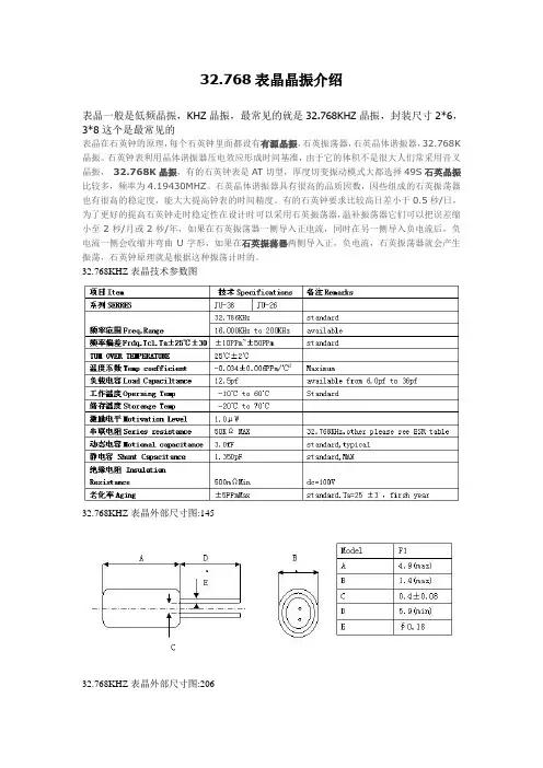
32.768表晶晶振介绍
表晶一般是低频晶振,KHZ晶振,最常见的就是32.768KHZ晶振,封装尺寸2*6,3*8这个是最常见的
表晶在石英钟的原理,每个石英钟里面都设有有源晶振,石英振荡器,石英晶体谐振器,32.768K 晶振。
石英钟表利用晶体谐振器压电效应形成时间基准,由于它的体积不是很大人们常采用音叉晶振,32.768K晶振,有的石英钟表是AT切型,厚度切变振动模式大都选择49S石英晶振比较多,频率为4.19430MHZ。
石英晶体谐振器具有很高的品质因数,因些组成的石英振荡器也有很高的稳定度,能大大提高钟表的时间精度。
有的石英钟要求比较高日差小于0.5秒/日,为了更好的提高石英钟走时稳定性在设计时可以采用石英振荡器,温补振荡器它们可以把误差缩小至2秒/月或2秒/年,如果在石英振荡器一侧导入正电流,同时在另一侧导入负电流后,负电流一侧会收缩并弯曲U字形,如果在石英振荡器两侧导入正,负电流,石英振荡器就会产生振荡,石英钟原理就是根据这种振荡计时的。
32.768KHZ表晶技术参数图
32.768KHZ表晶外部尺寸图:145
32.768KHZ表晶外部尺寸图:206
32.768KHZ表晶久尺寸图308。

32.768khz 温补晶振电路
32.768kHz温补晶振电路通常由一个晶体振荡器和一些辅助元件组成,其目的是为了稳定地提供32.768kHz的时钟信号。
这个信号广泛应用于各种数字集成电路中,如实时时钟(RTC)等,作为计时基准。
以下是一个基本的32.768kHz温补晶振电路的组成部分:
1. 晶体:核心元件是石英晶体,它具有非常高的Q值,可以产生3
2.768kHz 的振荡频率。
2. 反相器:通常采用CMOS反相器,它为晶体提供偏置,使晶体工作在饱和区,以获得较大的增益。
3. 负载电容:C1和C2是晶体的负载电容,与反相器一起形成一个负阻,为晶体提供振荡所需的能量。
4. 温度补偿电容:C3和C4是温度补偿电容,通常连接到晶体的两个端子,以稳定其振荡频率。
5. 电阻:R1和R2是电阻,用于降低对晶体的驱动能量,防止晶体振坏或出现异常。
6. 反相器:inv2对invl的输出波形进行整形并驱动负载。
在实际应用中,为了确保32.768kHz温补晶振电路的稳定性,通常需要接上一个电容来稳定其振荡频率。
这是因为石英晶体的振荡频率受到外界环境温度、机械振动等因素的影响,容易发生波动和漂移。
通过加入一个适当的电容,可以形成一个谐振回路,使得晶振的振荡频率在一定范围内保持稳定。
此外,32.768kHz温补晶振电路具有体积小、功耗低等优点,被广泛应用于各种小型电子设备中,如腕表、电子计时器、温度计、LCD屏幕驱动器等的时钟电路中。

NXP
电源管理IC > AC/DC转换器> 医用电源转换器> TEA1552T
TEA1552T DCM或QR模式下具有高压启动的反激控制Production 器;125kHzf-osc(h);可输出待机信号
GreenChipll是第二代绿色环保开关电源(SMPS)控制器IC,可直接使用整流后的全电压市电工作。
高集成度使电源应用只需极少的外部器件,因而经济有效。
专用内置绿色能特性可满足各种功率水平的高效运行需求。
这适用于高功率水平的准谐振工作,以及中等功率水平谷底开关的固定频率工作。
在低功耗(待机)水平,该系统在降频模式下工作,仍具有谷底检测。
恩智浦专用的高压BCD800工艺使得直接从整流过的市电电压启动成为可能,这种方式既有效又环保。
第二低压BICMOS芯片用于高速精确保护与控制。
使用GreenChipII控制IC可以轻松设计高效、可靠的电源。
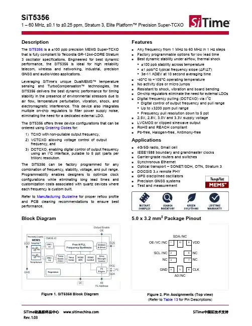
SiT53561 – 60 MHz, ±0.1 to ±0.25 ppm, Stratum 3, Elite Platform™ Precision Super-TCXODescriptionThe SiT5356 is a ±100 ppb precision MEMS Super-TCXO that is fully compliant to Telcordia GR-1244-CORE Stratum 3 oscillator specifications. Engineered for best dynamic performance, the SiT5356 is ideal for high reliability telecom, wireless and networking, industrial, precision GNSS and audio/video applications.L everaging SiTime’s unique DualMEMS™ temperature sensi ng and TurboCompensation™ technolog ies, the SiT5356 delivers the best dynamic performance for timing stability in the presence of environmental stressors due to air flow, temperature perturbation, vibration, shock, and electromagnetic interference. This device also integrates multiple on-chip regulators to filter power supply noise, eliminating the need for a dedicated external LDO.The SiT5356 offers three device configurations that can be ordered using Ordering Codes for:1)TCXO with non-pullable output frequency,2)VCTCXO allowing voltage control of outputfrequency, and3)DCTCXO, enabling digital control of output frequencyusing an I2C interface, pullable to 5 ppt (parts pertrillion) resolution.The SiT5356 can be factory programmed for any combination of frequency, stability, voltage, and pull range. Programmability enables designers to optimize clock configurations while eliminating long lead times and customization costs associated with quartz devices where each frequency is custom built.Refer to Manufacturing Guideline for proper reflow profile and PCB cleaning recommendations to ensure best performance. Features⏹Any frequency from 1 MHz to 60 MHz in 1 Hz steps ⏹Factory programmable options for low lead time⏹Best dynamic stability under airflow, thermal shock▪±100 ppb stability across temperature▪±1 ppb/ C typical frequency slope (ΔF/ΔT)▪3e-11 ADEV at 10 second averaging time⏹-40°C to +105°C operating temperature⏹No activity dips or micro jumps⏹Resistant to shock, vibration and board bending⏹On-chip regulators eliminate the need for external LDOs ⏹Digital frequency pulling (DCTCXO) via I2C▪Digital control of output frequency and pull range ▪Up to ±3200 ppm pull range▪Frequency pull resolution down to 5 ppt⏹ 2.5V, 2.8V, 3.0V and 3.3V supply voltage⏹LVCMOS or clipped sinewave output⏹RoHS and REACH compliant⏹Pb-free, Halogen-free, Antimony-free Applications⏹4G/5G radio, Small cell⏹IEEE1588 boundary and grandmaster clocks⏹Carrier-grade routers and switches⏹Synchronous Ethernet⏹Optical transport – SONET/SDH, OTN, Stratum 3⏹DOCSIS 3.x remote PHY⏹GPS disciplined oscillators⏹Precision GNSS systems⏹Test and measurementBlock DiagramFigure 1. SiT5356 Block Diagram 5.0 x 3.2 mm2 Package PinoutOE / VC / NC12345678910SCL / NCNCGNDNCNCVDDCLKA0 / NCSDA / NCFigure 2. Pin Assignments (Top view) (Refer to Table 13for Pin Descriptions)Ordering InformationThe following part number guide is for reference only. To customize and build an exact part number, use theSiTime Part Number Generator. To validate the part number, use the SiTime Part Number Decoder.Notes:1. “-“ corresponds to the default rise/fall time for LVCMOS output as specified in Table 1 (Electrical Characteristics). Contact SiTime for other rise/fall time optionsfor best EMI.2. Bulk is available for sampling onlyTABLE OF CONTENTSDescription (1)Features (1)Applications (1)Block Diagram (1)5.0 x 3.2 mm2 Package Pinout (1)Ordering Information (2)Electrical Characteristics (4)Device Configurations and Pin-outs (10)Pin-out Top Views (10)Test Circuit Diagrams for LVCMOS and Clipped Sinewave Outputs (11)Waveforms (13)Timing Diagrams (14)Typical Performance Plots (15)Architecture Overview (19)Frequency Stability (19)Output Frequency and Format (19)Output Frequency Tuning (19)Pin 1 Configuration (OE, VC, or NC) (20)Device Configurations (20)TCXO Configuration (20)VCTCXO Configuration (21)DCTCXO Configuration (22)VCTCXO-Specific Design Considerations (23)Linearity (23)Control Voltage Bandwidth (23)FV Characteristic Slope K V (23)Pull Range, Absolute Pull Range (24)DCTCXO-Specific Design Considerations (25)Pull Range and Absolute Pull Range (25)Output Frequency (26)I2C Control Registers (28)Register Descriptions (28)Register Address: 0x00. Digital Frequency Control Least Significant Word (LSW) (28)Register Address: 0x01. OE Control, Digital Frequency Control Most Significant Word (MSW) (29)Register Address: 0x02. DIGITAL PULL RANGE CONTROL[14] (30)Serial Interface Configuration Description (31)Serial Signal Format (31)Parallel Signal Format (32)Parallel Data Format (32)I2C Timing Specification (34)I2C Device Address Modes (35)Schematic Example (36)Dimensions and Patterns (37)Layout Guidelines (38)Manufacturing Guidelines (38)Electrical CharacteristicsAll Min and Max limits are specified over temperature and rated operating voltage with 15 pF output load unless otherwise stated. Typical values are at 25°C and 3.3V Vdd.Table 1. Output CharacteristicsTable 1. Output Characteristics (continued)Table 2. DC CharacteristicsTable 3. Input CharacteristicsNote:3. APR = PR – initial tolerance – 20-year aging – frequency stability over temperature. Refer to Table 17 for APR with respect to other pull range options.Table 5. Jitter & Phase Noise – Clipped Sinewave, -40 to 85 °CTable 7. Jitter & Phase Noise – Clipped Sinewave, -40 to 105 °CTable 8. Absolute Maximum LimitsAttempted operation outside the absolute maximum ratings may cause permanent damage to the part.Actual performance of the IC is only guaranteed within the operational specifications, not at absolute maximum ratings.Note:4. Exceeding this temperature for an extended period of time may damage the device.Table 9. Thermal Considerations[5]Note:5. Measured in still air.Table 10. Maximum Operating Junction Temperature[6]Note:6. Datasheet specifications are not guaranteed if junction temperature exceeds the maximum operating junction temperature.Table 11. Environmental ComplianceDevice Configurations and Pin-outsTable 12. Device ConfigurationsPin-out Top ViewsOE/NC12345678910NC NC GNDNC NC VDD CLKNCNCFigure 3. TCXOVC 12345678910NC NC GNDNC NC VDD CLKNCNCFigure 4. VCTCXOOE / NC 12345678910 SCL NC GNDNC NC VDD CLKA0 / NCSDAFigure 5. DCTCXOTable 13. Pin DescriptionNotes:7. In OE mode for noisy environments, a pull-up resistor of 10 kΩ or less is recommended if pin 1 is not externally driven. If pin 1 needs to be left floating, use the NC option.8. A 0.1 μF capacitor in parallel with a 10 μF capacitor are required between Vdd and GND. The 0.1 μF capacitor is recommended to place close to the device, and place the 10 μF capacitor less than 2 inches away.9. All NC pins can be left floating and do not need to be soldered down.Test Circuit Diagrams for LVCMOS and Clipped Sinewave OutputsFigure 6. LVCMOS Test Circuit (OE Function)Figure 7. Clipped Sinewave Test Circuit (OE Function)for AC and DC MeasurementsVC FunctionFigure 8. LVCMOS Test Circuit (VC Function)VC FunctionFigure 9. Clipped Sinewave Test Circuit (VC Function)for AC and DC MeasurementsNC FunctionFigure 10. LVCMOS Test Circuit (NC Function)NC FunctionFigure 11. Clipped Sinewave Test Circuit (NC Function)for AC and DC MeasurementsTest Circuit Diagrams for LVCMOS and Clipped Sinewave Outputs (continued)FunctionFigure 12. LVCMOS Test Circuit (I2C Control), DCTCXO modeFunction2C Control), DCTCXO mode for AC and DC MeasurementsFigure 13. Clipped Sinewave Test Circuit (IFigure 14. Clipped Sinewave Test Circuit for Phase Noise Measurements, Applies to All Configurations(NC Function shown for example only)Note:10.SDA is open-drain and may require pull-up resistor if not present in I2C test setup.Waveforms90 % Vdd 50 % Vdd10 % VddFigure 15. LVCMOS Waveform Diagram[11]Figure 16. Clipped Sinewave Waveform Diagram[11]Note:11.Duty Cycle is computed as Duty Cycle = TH/Period.Timing DiagramsVdd Pin CLK OutputT_start: Time to start from power-offFigure 17. Startup Timing T_oe: Time to re-enable the clock outputFigure 18. OE Enable Timing (OE Mode Only)Typical Performance PlotsFigure 19. ADEV (±0.1 ppm)Figure 20. TDEV (0.1 Hz loop bandwidth, ±0.1 ppm)Figure 21. MTIE (0.1 Hz loop bandwidth, ±0.1 ppm)Figure 22. Frequency vs Temperature (±0.1 ppm), 105°CFigure 23. Freq. vs. Temp. Slope (ΔF/ΔT), ±0.1 ppm deviceFigure 24. VCTCXO frequency pull characteristicFigure 25. 1-day aging rate (to 62 days), ±0.1 ppm deviceFigure 26. Drift over 30 days relative to the first readingTypical Performance Plots (continued)Figure 27. Load sensitivity (±0.1 ppm )Figure 28. VDD sensitivity (±0.1 ppm)Figure 31. IDD TCXO (LVCMOS)Figure 32. IDD VCTCXO (LVCMOS)Figure 33. T_phj, RMS Random, (DC)TCXO (LVCMOS)Figure 34. Period Jitter, RMS (LVCMOS)Figure 35. IDD DCTCXO (LVCMOS)Figure 36. T_phj, RMS Random, VCTCXO (LVCMOS)Figure 37. DCTCXO frequency pull characteristicFigure 38. Rise Time (Clipped Sinewave)Figure 39. IDD TCXO (Clipped Sinewave)Figure 40. IDD VCTCXO (Clipped Sinewave)Figure 41. T_phj, RMS Random, (DC)TCXO (Clipped Sine)Figure 42. IDD DCTCXO (Clipped Sinewave)Figure 43. T_phj, RMS Random, VCTCXO (Clipped Sine)Figure 44. Duty Cycle (Clipped Sinewave)Architecture OverviewBased on SiTime’s innovative Elite Platform™, the SiT5356 delivers exceptional dynamic performance, i.e. resilience to environmental stressors such as shock, vibration, and fast temperature transients. Underpinning the Elite platform are SiTime’s unique DualMEMS™temperature sensing architecture and TurboCompensation™ technologies. DualMEMS is a noiseless temperature compensation scheme. It consists of two MEMS resonators fabricated on the same die substrate. The TempFlat™resonator is designed with a flat frequency characteristic over temperature whereas the temperature sensing resonator is by design sensitive to temperature changes. The ratio of frequencies between these two resonators provides an accurate reading of the resonator temperature with 20 µK resolution.By placing the two MEMS resonators on the same die, this temperature sensing scheme eliminates any thermal lag and gradients between resonator and temperature sensor, thereby overcoming an inherent weakness of legacy quartz TCXOs.The DualMEMS temperature sensor drives a state-of-the-art CMOS temperature compensation circuit. The TurboCompensation design, with >100 Hz compensation bandwidth, achieves a dynamic frequency stability that is far superior to any quartz TCXO. The digital temperature compensation enables additional optimization of frequency stability and frequency slope over temperature within any chosen temperature range for a given system design.Figure 45. Elite ArchitectureThe Elite platform also incorporates a high resolution, low noise frequency synthesizer along with the industry standard I2C bus. This unique combination enables system designers to digitally control the output frequency in steps as low as 5 ppt and over a wide range up to ±3200 ppm. For more information regarding the Elite platform and its benefits please visit:⏹SiTime's breakthroughs section⏹TechPaper:DualMEMS Temperature Sensing Technology ⏹TechPaper:DualMEMS Resonator TDC Functional OverviewThe SiT5356 is designed for maximum flexibility with an array of factory programmable options, enabling system designers to configure this precision device for optimal performance in a given application.Frequency StabilityThe SiT5356 comes in two factory-trimmed stability grades that are optimized for different applications. Both Stratum 3+ and Stratum 3 devices are compliant with Stratum 3 stability of ±4.6 ppm over 20 years.Table 14. Stability Grades vs. Ordering Codes⏹Stratum 3+ grade with ΔF/ΔT of ±3.5 ppb/︒C isengineered to provide significantly better performancethan legacy quartz TCXOs in time and phasesynchronization applications such as IEEE1588, smallcells, and 5G C-RAN (cloud RAN).⏹Stratum 3 grade is designed to replace classicStratum 3 TCXOs in applications such as SyncE withbetter dynamic performance and shorter lead time. Output Frequency and FormatThe SiT5356 can be factory programmed for an outputfrequency without sacrificing lead time or incurring an upfront customization cost typically associated with custom-frequency quartz TCXOs.The device supports both LVCMOS and clipped sinewave output. Ordering codes for the output format are shown below: Table 15. Output Formats vs. Ordering CodesOutput Frequency TuningIn addition to the non-pullable TCXO, the SiT5356 can also support output frequency tuning through either an analog control voltage (VCTCXO), or I2C interface (DCTCXO). The I2C interface enables 16 factory programmed pull-range options from ±6.25 ppm to ±3200 ppm. The pull range can also be reprogrammed via I2C to any supported pull-range value.Refer to Device Configuration section for details.Pin 1 Configuration (OE, VC, or NC)Pin 1 of the SiT5356 can be factory programmed to support three modes: Output Enable (OE), Voltage Control (VC), or No Connect (NC).Table 16. Pin Configuration OptionsWhen pin 1 is configured as OE pin, the device output is guaranteed to operate in one of the following two states:⏹Clock output with the frequency specified in the partnumber when Pin 1 is pulled to logic high⏹Hi-Z mode with weak pull down when pin 1 is pulled tologic low.When pin 1 is configured as NC, the device is guaranteed to output the frequency specified in the part number at all times, regardless of the logic level on pin 1.In the VCTCXO configuration, the user can fine-tune the output frequency from the nominal frequency specified in the part number by varying the pin 1 voltage. The guaranteed allowable variation of the output frequency is specified as pull range. A VCTCXO part number must contain a valid pull-range ordering code. Device ConfigurationsThe SiT5356 supports 3 device configurations –TCXO,VCTCXO, and DCTCXO. The TCXO and VCTCXO options are directly compatible with the quartz TCXO and VCTCXO. The DCTCXO configuration provides performance enhancement by eliminating VCTCXO’s sensitivity to control voltage noise with an I2C digital interface for frequency tuning.Figure 46. Block Diagram – TCXOTCXO ConfigurationThe TCXO configuration generates a fixed frequency output, as shown in Figure 46. The frequency is specified by the user in the frequency field of the device ordering code and then factory programmed. Other factory programmable options include supply voltage, output types (LVCMOS or clipped sinewave), and pin 1 functionality (OE or NC).Refer to the Ordering Information section at the end of the datasheet for a list of all ordering options.A VCTCXO, shown in Figure 47, is a frequency control device whose output frequency is an approximately linear function of control voltage applied to the voltage control pin. VCTCXOs have a number of use cases including the VCO portion of a jitter attenuation/jitter cleaner PLL Loop.The SiT5356 achieves a 10x better pull range linearity of <0.5% via a high-resolution fractional PLL compared with 5% to 10% typical of quartz VCTCXOs that rely on pulling a resonator. By contrast, quartz-based VCTCXOs change output frequency by varying the capacitive load of a crystal resonator using varactor diodes, which results in poor linearity.Figure 47. Block Diagram – VCTCXO Note that the output frequency of the VCTCXO is proportional to the analog control voltage applied to pin 1. Because this control signal is analog and directly controls the output frequency, care must be taken to minimize noise on this pin.The nominal output frequency is factory programmed per the customer’s request to 6 digits of precision and is defined as the output frequency when the control voltage equals Vdd/2. The maximum output frequency variation from this nominal value is set by the pull range, which is also factory programmed to the customer’s desired value and specified by the ordering code. The Ordering Information section shows all ordering options and associated ordering codes. Refer to VCTCXO-Specific Design Considerations for more information on critical VCTCXO parameters including pull range linearity, absolute pull range,control voltage bandwidth, and Kv.The SiT5356 offers digital control of the output frequency, as shown in Figure 48. The output frequency is controlled by writing frequency control words over the I2C interface. There are several advantages of DCTCXOs relative to VCTCXOs:1)Frequency control resolution as low as 5 ppt. Thishigh resolution minimizes accumulated time error insynchronization applications.2)Lower system cost – A VCTCXO may need a Digital toAnalog Converter (DAC) to drive the control voltageinput. In a DCTXCO, the frequency control is achieveddigitally by register writes to the control registers viaI2C, thereby eliminating the need for a DAC.3)Better noise immunity –The analog signal used todrive the voltage control pin of a VCTCXO can besensitive to noise, and the trace over which the signalis routed can be susceptible to noise coupling from thesystem. The DCTCXO does not suffer from analognoise coupling since the frequency control isperformed digitally through I2C.Figure 48. Block Diagram4)No frequency-pull non-linearity – The frequency pullingis achieved via fractional feedback divider of the PLL, eliminating any pull non-linearity concerns typical of quartz-based VCTCXOs. This improves dynamic performance in closed-loop applications.5)Programmable wide pull range –The DCTCXOpulling mechanism is via the fractional feedback divider and is therefore not constrained by resonator pullability as in quartz-based solutions. The SiT5356 offers 16 frequency pull-range options from ±6.25ppm to ±3200ppm, providing system designers great flexibility.Refer to DCTCXO-Specific Design Considerations for more information on critical DCTCXO parameters including pull range, absolute pull range, frequency output, and I2Ccontrol registers.VCTCXO-Specific Design ConsiderationsLinearityIn any VCTCXO, there will be some deviation of the frequency-voltage (FV) characteristic from an ideal straight line. Linearity is the ratio of this maximum deviation to the total pull range, expressed as a percentage. Figure 49 below shows the typical pull linearity of a SiTime VCTCXO. The linearity is excellent (1% maximum) relative to most quartz offerings because the frequency pulling is achieved with a PLL rather than varactor diodes.Figure 49. Typical SiTime VCTCXO LinearityControl Voltage BandwidthControl voltage b andwidth, sometimes called “modulation r ate” or “modulation b andwidth”, indicates how fast a VCO can respond to voltage changes at its input. The ratio of the output frequency variation to the input voltage variation, previously denoted by K V, has a low-pass characteristic in most VCTCXOs. The control voltage bandwidth equals the modulating frequency where the output frequency deviation equals 0.707 (e.g. -3 dB) of its DC value, for DC inputs swept in the same voltage range.For example, a part with a ±6.25 ppm pull range and a 0-3V control voltage can be regarded as having an average KV of 4.17 ppm/V (12.5 ppm/3V = 4.17 ppm/V). Applying an input of 1.5V DC ± 0.5V (1.0 V to 2.0V) causes an output frequency change of 4.17 ppm (±2.08 ppm). If the control voltage bandwidth is specified as 10 kHz, the peak-to-peak value of the output frequency change will be reduced to 4.33 ppm/√2 or 2.95 ppm, as the frequency of the control voltage change is increased to 10 kHz.FV Characteristic Slope K VThe slope of the FV characteristic is a critical design parameter in many low bandwidth PLL applications. The slope is the derivative of the FV characteristic –the deviation of frequency divided by the control voltage change needed to produce that frequency deviation, over a small voltage span, as shown below:inoutV VfK∆∆=It is typically expressed in kHz/Volt, MHz/Volt, ppm/Volt, or similar units. This s lope is usually called “K V” based on terminology used in PLL designs.The extreme linear characteristic of the SiTime SiT5356 VCTCXO family means that there is very little K V variation across the whole input voltage range (typically <1%), significantly reducing the design burden on the PLL designer. Figure50below illustrates the typical K V variation.Figure 50. Typical SiTime K V VariationPull Range, Absolute Pull RangePull range (PR) is the amount of frequency deviation that will result from changing the control voltage over its maximum range under nominal conditions.Absolute pull range (APR) is the guaranteed controllable frequency range over all environmental and aging conditions. Effectively, it is the amount of pull range remaining after taking into account frequency stability, tolerances over variables such as temperature, power supply voltage, and aging, i.e.:agingstability F F PR APR --=where stability F is the device frequency stability due to initial tolerance and variations on temperature, power supply, and load.Figure 51 shows a typical SiTime VCTCXO FV characteristic. The FV characteristic varies with conditions, so that the frequency output at a given input voltage can vary by as much as the specified frequency stability of the VCTCXO. For such VCTCXOs, the frequency stability and APR are independent of each other. This allows very wide range of pull options without compromising frequency stability.Figure 51. Typical SiTime VCTCXO FV Characteristic The upper and lower control voltages are the specified limits of the input voltage range as shown in Figure 51 above. Applying voltages beyond the upper and lower voltages do not result in noticeable changes of output frequency. In other words, the FV characteristic of the VCTCXO saturates beyond these voltages. Figures 1 and 2 show these voltages as Lower Control Voltage (VC_L) and Upper Control Voltage (VC_U).Table 17 below shows the pull range and corresponding APR values for each of the frequency vs. temperature ordering options.Table 17. VCTCXO Pull Range, APR Options [12] Typical unless specified otherwise. Pull range (PR) is ±6.25 ppm.Notes:12.APR includes initial tolerance, frequency stability vs. temperature, and the corresponding 20-year aging.DCTCXO-Specific Design ConsiderationsPull Range and Absolute Pull RangePull range and absolute pull range are described in theprevious section. Table 18 below shows the pull range andcorresponding APR values for each of the frequency vs.temperature ordering options.Table 18. APR Options[13]Notes:13.APR includes initial tolerance, frequency stability vs. temperature, and the corresponding 20-year aging.Output FrequencyThe device powers up at the nominal operating frequency and pull range specified by the ordering code. After power-up both pull range and output frequency can be controlled via I2C writes to the respective control registers. The maximum output frequency change is constrained by the pull range limits.The pull range is specified by the value loaded in the digital pull-range control register. The 16 pull range choices are specified in the control register and range from ±6.25ppm to ±3200ppm.Table 19 below shows the frequency resolution versus pull range programmed valueTable 19. Frequency Resolution versus Pull RangeThe ppm frequency offset is specified by the 26 bit DCXO frequency control register in two’s complement format as described in the I2C Register Descriptions. The power up default value is 00000000000000000000000000b which sets the output frequency at its nominal value (0 ppm). To change the output frequency, a frequency control word is written to 0x00[15:0] (Least Significant Word) and 0x01[9:0] (Most Significant Word). The LSW value should be written first followed by the MSW value; the frequency change is initiated after the MSW value is written.Figure 52. Pull Range and Frequency Control WordFigure 52shows how the two’s complement signed value of the frequency control word sets the output frequency within the ppm pull range set by 0x02:[3:0]. This example shows use of the ±200 ppm pull range. Therefore, to set the desired output frequency, one just needs to calculate the fraction of full scale value ppm, con vert to two’s complement binary, and then write these values to the frequency control registers.The following formula generates the control word value: Control word value = RND((225-1) × ppm shift from nominal/pull range), where RND is the rounding function which rounds the number to the nearest whole number. Two examples follow, assuming a ±200 ppm pull range: Example 1:⏹Default Output Frequency = 19.2 MHz⏹Desired Output Frequency = 19.201728 MHz (+90 ppm) 225-1 corresponds to +200 ppm, and the fractional value required for +90 ppm can be calculated as follows.⏹90 ppm / 200 ppm × (225-1) = 15,099,493.95.Rounding to the nearest whole number yields 15,099,494 and converting to two’s complement gives a binary value of 111001100110011001100110, or E66666 in hex.Example 2:⏹Default Output Frequency = 10 MHz⏹Desired Output Frequency = 9.998 MHz (-50 ppm) Following the formula shown above,⏹(-50 ppm / 200 ppm) × (225-1) = -8,388,607.75. Rounding this to the nearest whole number results in-8,388,608.Converting this to two’s complement binary results in 11100000000000000000000000, or 3800000 in hex. To summarize, the procedure for calculating the frequency control word associated with a given ppm offset is as follows:1)Calculate the fraction of the half-pull range needed.For example, if the total pull range is set for ±100 ppmand a +20 ppm shift from the nominal frequency isneeded, this fraction is 20 ppm/100 ppm = 0.22)Multiply this fraction by the full-half scale word value,225-1 = 33,554,431, round to the nearest wholenumber, and convert the result to two’s complementbinary. Following the +20ppm example, this value is0.2 × 33,554,431 = 6,710,886.2 and rounded to6,710,886.3)Write the two’s complement binary value starting withthe Least Significant Word (LSW) 0x00[16:0],followed by the Most Significant Word (MSW),0x01[9:0]. If the user desires that the output remainsenabled while changing the frequency, a 1 must alsobe written to the OE control bit 0x01[10] if the devicehas software OE Control Enabled.It is important to note that the maximum Digital Control update rate is 38 kHz regardless of I2C bus speed.I2C Control RegistersThe SiT5356 enables control of frequency pull range, frequency pull value, and Output Enable via I2C writes to the control registers. Table 20 below shows the register map summary, and detailed register descriptions follow.Table 20. Register Map SummaryRegister DescriptionsRegister Address: 0x00. Digital Frequency Control Least Significant Word (LSW)。
•Extensive portfolio •Enables longer battery life •Ultra-small footprint• B etter performance and higher stabilityin harsh environments• P rogrammable, instant samples,shorter lead timeMEMS Timing Solutions forMobile and IoTA small part fromSiTime runs a big part of your worldSiT1532 Oscillatorsand SiT1566, SiT1572, SiT1576, SiT1580 TCXOs•Smallest footprint | 1.5 x 0.8 mm chip scale package•Drives multiple loads | Optimized BOM & smaller form factor •High integration | Optimized BOM & smaller form factorSmartphone & Mobile AccessoriesMEMS Timing Improves Mobile and IoTSiT1569, SiT8021 Oscillators and SiT1566, SiT1580 TCXOs• 3 ppm stability | Higher accuracy enables longer sleep mode •Smallest footprint | 1.5 x 0.8 mm chip scale package•1 Hz to 2.5 MHz frequency | Wide range of custom frequenciesStylus & TabletsSiT1532, SiT1534, SiT1580 Oscillators and SiT1552 TCXOs•Low power | < 1 µa, NanoDrive™ output to optimize swing •Smallest footprint | 1.5 x 0.8 mm chip scale package •High robustness | Immune to small molecular gassesFitness TrackerSiT1532 Oscillatorsand SiT1552, SiT1580 TCXOs•Low power | < 1 µa, NanoDrive™ output to optimize swing •Smallest footprint | 1.5 x 0.8 mm chip scale package •High robustness | Immune to small molecular gassesSmart WatchSiT1532, SiT1579 Oscillators and SiT1576 TCXOs•Smallest footprint | 1.5 x 0.8 mm chip scale package •Drives multiple loads | Optimized BOM•1 Hz to 2.5 MHz frequency | Wide range of custom frequenciesGlasses/VRSiT1532, SiT1579 Oscillators and SiT1576, SiT1580 TCXOs• 1 Hz to 2.5 MHz frequency | Wide range of custom frequencies •Package options | 1.5 x 0.8 mm CSP , QFN, SoT23•High reliability | Low DPPMRemote SensingMEMS Timing Outperforms QuartzSmallest Size, Lower BOMBest 32 kHz StabilitySiT153x MEMS XOMeasuredLower PowerMEMS XODrive Multiple LoadsLow Power FeatureMEMS XOSiT153x 25°C Stability SpecField Programmable Oscillators – Always AvailableEasy-to-use programming kit•••。
32.786晶振参数一、晶振参数概述晶体振荡器,或简称晶振,是一个重要的电子元件,主要用于产生振荡频率。
其工作原理基于晶体在受到物理冲击或电场变化时,会产生机械振动,这种振动又会产生电场变化,进而形成电压输出。
晶振的参数是描述其性能和特性的重要指标,对于其应用和选择具有重要意义。
二、晶振的主要参数1.频率范围:指晶振所能产生的振荡频率范围。
不同的晶振有不同的频率范围,根据应用需求选择合适的频率范围是关键。
2.精度:指晶振的输出频率的准确性。
一般来说,晶振的频率精度越高,其性能越好。
3.温度稳定性:指晶振在温度变化下的频率稳定性。
温度稳定性是衡量晶振性能的重要指标,对于需要高精度频率源的应用尤为重要。
4.负载电容:指晶振在实际应用中所需的最小电容值。
负载电容会影响晶振的输出频率,因此在实际应用中需要特别注意。
5.激励电平:指驱动晶振的电压或电流大小。
过大的激励电平可能会损坏晶振,过小的激励电平则可能导致晶振无法正常工作。
6.输出波形:指晶振输出的信号波形。
一般来说,晶振输出的波形为正弦波或方波。
三、晶振的测试与验证为了确保晶振的性能和可靠性,需要进行一系列的测试与验证。
这些测试包括但不限于:1.频率精度测试:通过专用测试设备对晶振的输出频率进行测量,以评估其精度。
2.温度稳定性测试:在不同的温度环境下测试晶振的频率变化情况,以评估其在不同温度下的性能。
3.负载电容测试:测量晶振在不同负载电容下的输出频率,以确定其最佳工作条件。
4.激励电平测试:测量晶振在不同激励电平下的性能表现,以确定其正常工作范围。
5.长期老化测试:长时间运行晶振以评估其性能随时间的退化程度,这是确保晶振可靠性必不可少的环节。
通过以上测试与验证,可以对晶振的性能有一个全面、深入的了解,从而为其应用和选择提供可靠的依据。
四、晶振的应用与选择晶振的应用非常广泛,如通信、导航、电子测量、自动控制等领域。
在选择晶振时,需要考虑以下因素:1.应用需求:不同的应用对晶振的性能要求不同,应根据实际需求进行选择。
【SITIME中国区样品与大批量现货量产中心 - 深圳扬兴科技有限公司】www.yxc.hk SiT1566 1.2mm2 Micropower, 5 ppm, Low-Jitter 32.768 kHz Super TCXO5°C/sec Temp Ramp Frequency Response 10°C/sec Temp Ramp Frequency Response ~10°C/sec ~5°C/sec [3] [3] 3 Hz Temp Comp Refresh Rate 3 Hz Temp Comp Refresh Rate For temperature ramps >5°C/sec, the frequency accuracy is limited by the update rate of the temperature compensation path (see the 5°C/sec and 10°C/sec plots. Contact Factory for applications that require improved dynamic performance. Note: 3. Measured relative to 32.768 kHz. Rev. 0.7 Page 6 of 8 【SITIME中国区样品与大批量现货量产中心 - 深圳扬兴科技有限公司】www.yxc.hk SiT1566 1.2mm2 Micropower, 5 ppm, Low-Jitter 32.768 kHz Super TCXO– Dimensions (Unit: mm 1.55 x 0.85 mm CSP 1.54 ±0.04 Recommended Land Pattern (Unit: mm 0.84 ±0.04 #4 #3 #3 0.315 ±0.015 #4 #4 #3 #1 #2 #2 #1 #1 #2 Recommend 4-mil (0.1mm stencilthickness Manufacturing Guidelines 1 2 3 4 No Ultrasonic or Megasonic cleaning: Do not subject SiT1566 to an ultrasonic or megasonic cleaning environment. Permanent damage or long term reliability issues may occur. Applying board-level underfill and overmold is acceptable and will not impact the reliability of the device. Reflow profile, per JESD22-A113D. For additional manufacturing guidelines and marking/tape-reel instructions, click on the following link:/component/docman/doc_download/243-manufacturing-notes-for-sitimeoscillators Rev. 0.7 Page 7 of 8 【SITIME中国区样品与大批量现货量产中心 - 深圳扬兴科技有限公司】www.yxc.hk SiT1566 1.2mm2 Micropower, 5 ppm, Low-Jitter 32.768 kHz Super TCXO566AI-JE-DCC-32.768S Part Family “SiT1566” Revision Letter “A”: is the revision Temperature Range “C”: Extended Commercial, -20 to 70ºC “I”: lndustrial, -40 to 85ºC Output Clock Frequency (kHz 32.768 kHz Packaging “S”: 8 mm Tape & Reel, 10ku reel “D”: 8 mm Tape & Reel, 3ku reel “E”: 8 mm Tape & Reel, 1ku reel Samples in cut Tape Package Size “J”: 1.5 mm x 0.8 mm CSP All-Inclusive Over Temp Stability “E”: ±5 ppm LVCMOS Output Revision History Revision 0.1 0.7 Release Date 6/30/15 3/11/16 Change Summary Advanced datasheet initial release Preliminary datasheet initial release © SiTime Corporation 2016. The information contained herein is subject to change at any time without notice. SiTime assumes no responsibility or liability for any loss, damage or defect of a Product which is caused in whole or in part by (i use of any circuitry other than circuitry embodied in a SiTime product, (ii misuse or abuse including static discharge, neglect or accident, (iii unauthorized modification or repairs which have been soldered or altered during assembly and are not capable of being tested by SiTime under its normal test conditions, or (iv improper installation, storage, handling, warehousing or transportation, or (v being subjected to unusual physical, thermal, or electrical stress. Disclaimer: SiTime makes no warranty of any kind, express or implied, with regard to this material, and specifically disclaims any and all express or implied warranties, eitherin fact or by operation of law, statutory or otherwise, including the implied warranties of merchantability and fitness for use or a particular purpose, and any implied warranty arising from course of dealing or usage of trade, as well as any common-law duties relating to accuracy or lack of negligence, with respect to this material, any SiTime product and any product documentation. Products sold by SiTime are not suitable or intended to be used in a life support application or component, to operate nuclear facilities, or in other mission critical applications where human life may be involved or at stake. All sales are made conditioned upon compliance with the critical uses policy set forth below. CRITICAL USE EXCLUSION POLICY BUYER AGREES NOT TO USE SITIME'S PRODUCTS FOR ANY APPLICATION OR IN ANY COMPONENTS USED IN LIFE SUPPORT DEVICES OR TO OPERATE NUCLEAR FACILITIES OR FOR USE IN OTHER MISSION-CRITICAL APPLICATIONS OR COMPONENTS WHERE HUMAN LIFE OR PROPERTY MAY BE AT STAKE. SiTime owns all rights, title and interest to the intellectual property related to SiTime's products, including any software, firmware, copyright, patent, or trademark. The sale of SiTime products does not convey or imply any license under patent or other rights. SiTime retains the copyright and trademark rights in all documents, catalogs and plans supplied pursuant to or ancillary to the sale of products or services by SiTime. Unless otherwise agreed to in writing by SiTime, any reproduction, modification, translation, compilation, or representation of this material shall be strictly prohibited. Rev. 0.7 Page 8 of 8。
二颗“高精确度、低功耗、小体积”32.768Khz 温补晶体振荡器TCXO 二颗32.768Khz 温补晶体振荡器TCXO的应用方案 DSK321STD 32.768Khz TCXO是上海唐辉电子有限公司目前面向市场推出的一款小体积、高精确度、低功耗的RTC温度补偿石英晶振。
对于目前兴起的智能穿戴市场以及物联网市场、智能医疗、手持式设备、智慧能源等领域来说,DSK321STD这颗产品给工程师们提供了一个非常不错的参考选择。
以智能穿戴产品为例,一般来说需要两个32.768kHz的参考时钟,一个用于MCU的RTC;一个用于蓝牙芯片的睡眠时钟。
如果使用晶体谐振器则需要采用两颗32.768Khz。
由于DSK321STD是一个时钟石英晶体振荡器,它可以很容易驱动两个负载,体现了该产品的优越性。
DSK321STD 32.768Khz TCXO的优势如下:1、采用数字温度补偿方式2、高精确度+/-5ppm(-40-+85°C)、+/-3.8ppm(-10-+60°C)3、低功耗4、宽工作电压范围(2.0V-5.5V)5、宽工作温度(-40-+105°C)6、小体积封装3.2*2.5mm7、无需防湿包装管理8、符合AEC-Q100标准主要参数如下:DSK321STD 32.768Khz实物图:DSK321STD 32.768Khz温度曲线图:DSK321STD 32.768Khz TCXO从2013年底问世以来,在唐辉电子的大力推广之下,目前已经有诸多典型的应用案例,与一些知名品牌的MCU匹配使用:1、德州仪器TI的 MSP430系列2、意法STmicro的STM32系列3、日本瑞萨Renesas的RL78系列4、 Microchip额PIC18/MCP794xx系列5、 Energy Micro的EFG32系列6、 Fujitsu的MB89xx/MB951xx系列7、 NXPDE LPC11xx系列8、 Freescale的L4x/L5x系列第二颗32.768Khz简介如下。
32.786晶振参数-回复什么是32.786晶振参数?32.786晶振参数是指用于数字系统中的一种晶体振荡器。
晶体振荡器是一种电子元件,它能够产生一个稳定的频率信号,并常被用于时钟系统、通信系统以及计算机等领域。
而32.786晶振则代表着这个晶振器所产生的频率为32.786kHz。
为什么使用32.786晶振参数?在数字系统中,时钟信号是十分重要的,它是决定整个系统工作速度以及正确运行的关键因素之一。
因此,选择一个适当的时钟源对于数字系统的稳定性和可靠性至关重要。
而32.786晶振参数则因其特殊的频率,适用于一些特定的应用场景。
一种常见的情况是,在一些精密的计算和测量场合,需要使用高分辨率的时钟源。
由于32.786晶振的频率较低且稳定性较高,因此能够满足这种高精度测量的要求。
在一些频率发生器、信号处理以及高精度测量仪器中,32.786晶振参数的应用相对较为常见。
另外,32.786晶振也广泛应用于实时时钟(Real-Time Clock)芯片中。
实时时钟用于提供系统时间和日期等功能,它需要一个稳定的时钟源。
而32.786kHz频率的晶振能够提供足够精度的时钟信号,用于满足实时时钟芯片的要求。
如何选择和设计32.786晶振参数?选择和设计32.786晶振参数首先需要考虑系统对时钟源的要求。
在选择晶振频率时,要综合考虑系统的精度、功耗以及成本等因素。
如果系统对精度要求较高,可以选择较高频率的晶振;如果系统对功耗要求较高,可以选择较低频率的晶振。
而32.786kHz频率的晶振则位于较低频谱,其优势在于功耗较低、成本相对较低且能满足一些特定应用场景的要求。
设计32.786晶振参数还需要考虑其他一些因素,例如晶振的工作温度范围、振荡器的稳定性以及电路的布局和封装等。
晶振的工作温度范围需要与系统环境相匹配,以确保晶振在各种温度条件下都能稳定工作。
晶振的稳定性是指晶振在各种环境条件下频率稳定性的能力,通常用ppm(百万分之一)来表示。