OB6563_Datasheet_Highray_071113
- 格式:pdf
- 大小:388.35 KB
- 文档页数:13

o T l
圖3 OB6561P 功能框圖1. 主要公式為便於理解功率因數校正變換器的設計,本節給出了系統開關頻率、功率器件的有效電流、輸出紋波電壓等重要參數的理論計算公式。
為簡化分析過程,作如下假設:A 所有功率開關、二極管、電感器、電容器等等均為理想元件。
B 由於功率開關的開關頻率遠遠高於輸入交流電壓頻率,故認爲在一個開關周期内,交流輸入電
壓和輸出電壓均為恆定值。
C 輸入交流電壓,電流為理想的正弦波,功率因數等於1.1基本等式根據基本的電工學原理,可以得出交流輸入端的幾個基本等式:交流輸入電壓V 2in(RMS) eq. 1)
交流輸入電流有效值in(RMS)
in(avg)V P =
eq. 2)
交流輸入電流
O
n -r
i g h t
C
o n
f i d
e n t
i a
l T
o y
c n -
T e
圖6 同樣根據電工學原理,鋸齒波的有效電流與峰值電流之比是3
D
,在一個開關周期内流經功率開關)sin(ωt ∗。

GENERAL DESCRIPTIONOB6663L integrates a transition mode power factor correction (TM PFC) controller and a Quasi-Resonant (QR) controller in one chip. The controller provides a cost effective solution for optimizing the power factor of LED lighting application power supply. QR provides higher efficiency and lower EMI compared to conventional PWM system. OB6663L provides high level integration and high performance than conventional PFC/PWM system. The built-in dual output control for TM PFC optimizes power conversion efficiency with reduced system cost. Separate analog ground (AGND) and power ground (PGND) provide better noise immunity. OB6663L features many built-in green functions to optimize power conversion efficiency at all power levels. This holds for QR operation at high power levels, as well as PFM operation at lower powerlevels, and ‘Extended Burst Mode’ operation at very low power or zero power (Standby) levels. At low power levels, OB6663L automatically turns off the PFC stage. In this way, low standby (<0.2W) together with low system cost can be achieved. OB6663L offers comprehensive protection coverage including VCC Under Voltage Lockout (UVLO), Cycle-by-Cycle Current Limiting for PFC and QR Stage (OCP), Output Over Voltage Protection for PFC and QR Stage (OVP), Open Loop Protection for PFC and QR Stage (OLP), Programmable Brownout Protection (BOP), Programmable Over Temperature Protection (OTP), Built-in Soft Start in QR Stage, VCC Zener Clamp, Gate Clamp, Pin Floating Protection, and External Latch Triggering, etc. OB6663L is offered in SOP-16 packages.FEATURES■ Integrated Transition Mode (TM) PFC Controller and Quasi-Resonant (QR) PWMController■ Built-in Dual Output PFC Control ■ Multi-Mode Operation for QR Stage■ Separate AGND and PGND Provide Better Noise Immunity ■ Analog Multiplier with Built-in THD Optimizer for PFC Stage■ Line Feed-forward Compensation for PFC Stage■ Enhanced Dynamic Response for PFC Stage ■ Less than 200mW Standby Power Consumption ■ Minimum QR Short Circuit Power Consumption ■ Audio Noise Free Operation PROTECTIONS ■ Precise Output Over Voltage Protection (OVP) for Both Converters ■ Open Loop Protection (OLP) for Both Converters■ Cycle-by-Cycle Current Limiting for Both Converters ■ 125KHz Max Frequency Clamping for QR Converter, and 240Khz for PFC converter ■ Programmable Brownout Protection (BOP)■ External Programmable Over Temperature Protection (OTP)■ External Latch Triggering for Both Converters ■ Minimum OFF time for Ringing Suppression ■ Maximum ON Time Limit for QR Converter ■ Built-in 4ms Soft Start for QR Converter ■ Internal Leading Edge Blanking for Both Converters ■ All Pin Floating Protection■ 1A Gate Drive Capability APPLICATIONSOffline AC/DC flyback converter for■ Power Adaptor and Open-frame SMPS ■ LCD Monitor/TV/PC ■ NotebookOn -B ri gh tCo n f i de n ti al to 合明光电TYPICAL APPLICATIONnoGENERAL INFORMATIONOrdering Information Part Number OB6663LQP 16 Pin SOP, Pb free in Tube OB6663LQPA 16 Pin SOP, Pb free in T&R Note: All Devices are offered in Pb-free Package if nototherwise noted.n -B ri n f i de nMarking InformationDescriptionIZero current detection input. When activated, a new PFC switchingcycle starts.I/O Input of multiplier. Connected to line voltage after bridge diodes via aresistor divider to provide sinusoidal reference voltage to the PFCcurrent loop. This pin is also used for brownout detection.3 INV IInverting input of the error amplifier (EA). The information at the outputof the PFC stage is fed to the pin through a resistor divider.I/O Output of EA. A compensation network is placed between COMP andAGND to achieve stability of the voltage control loop and ensure highpower factor and low THD.This pin is connected to AGND via a 20K Ohm resistor. Chip analog ground.I/OQR stage feedback input from the opto-coupler. The voltage of this pin controls the mode of QR operation in one of the three modes: Quasi-Resonant (QR), Pulse Frequency Modulation (PFM), and Burst Mode (BM).QR stage current sense input pin.I/OThis pin is connected to ground via a NTC resistor, external overtemperature protection.11 DEM IInput from QR auxiliary winding for demagnetization timing. This pin isalso used for QR over voltage protection.Chip power supply pin. QR stage totem pole gate driver output. PFC stage totem pole gate driver output. Chip power ground pin for PFC and QR gate driver PFC current sense input.RECOMMENDED OPERATING CONDITIONVCC Supply VoltageCo n f i de n ti aELECTRICAL CHARACTERISTICScurrent under normal operationTr_pfc PFC_OUT rising time Tf_pfc PFC_OUT falling timeQR Over Load Protection (QR OLP)Power Limiting FBPackage Mechanical Data:Dimensions In Millimeters Dimensions In Inches SymbolMin Max Min Max A1.350 1.750 0.053 0.069 A1 0.100 0.250 0.004 0.010 B ri gh t Co n f i de n ti al to 合明光电。

December 2010Doc ID 16116 Rev 41/43L6563SEnhanced transition-mode PFC controllerFeatures■Tracking boost function■Fast “bidirectional” input voltage feedforward (1/V 2 correction)■Interface for cascaded converter's PWM controller■Remote ON/OFF control■Accurate adjustable output overvoltage protection■Protection against feedback loop disconnection (latched shutdown)■Inductor saturation protection ■Low (≤ 100 µA) start-up current ■ 6 mA max. operating bias current■1% (@ T J = 25 °C) internal reference voltage ■-600/+800 mA totem pole gate driver with active pull-down during UVLO■SO14 package ApplicationsPFC pre-regulators for:■High-end AC-DC adapter/charger ■Desktop PC, server, Web server■IEC61000-3-2 or JEITA-MITI compliant SMPS, in excess of 400 WContents L6563SContents1Description . . . . . . . . . . . . . . . . . . . . . . . . . . . . . . . . . . . . . . . . . . . . . . . . . 62Maximum ratings . . . . . . . . . . . . . . . . . . . . . . . . . . . . . . . . . . . . . . . . . . . . 72.1Absolute maximum ratings . . . . . . . . . . . . . . . . . . . . . . . . . . . . . . . . . . . . . 72.2Thermal data . . . . . . . . . . . . . . . . . . . . . . . . . . . . . . . . . . . . . . . . . . . . . . . 7 3Pin connection . . . . . . . . . . . . . . . . . . . . . . . . . . . . . . . . . . . . . . . . . . . . . . 8 4Electrical characteristics . . . . . . . . . . . . . . . . . . . . . . . . . . . . . . . . . . . . 11 5Typical electrical performance . . . . . . . . . . . . . . . . . . . . . . . . . . . . . . . . 156Application information . . . . . . . . . . . . . . . . . . . . . . . . . . . . . . . . . . . . . 236.1Overvoltage protection . . . . . . . . . . . . . . . . . . . . . . . . . . . . . . . . . . . . . . . 236.2Feedback failure protection (FFP) . . . . . . . . . . . . . . . . . . . . . . . . . . . . . . 246.3Voltage feedforward . . . . . . . . . . . . . . . . . . . . . . . . . . . . . . . . . . . . . . . . . 246.4THD optimizer circuit . . . . . . . . . . . . . . . . . . . . . . . . . . . . . . . . . . . . . . . . 276.5Tracking boost function . . . . . . . . . . . . . . . . . . . . . . . . . . . . . . . . . . . . . . . 286.6Inductor saturation detection . . . . . . . . . . . . . . . . . . . . . . . . . . . . . . . . . . 306.7Power management/housekeeping functions . . . . . . . . . . . . . . . . . . . . . . 31 7Application examples and ideas . . . . . . . . . . . . . . . . . . . . . . . . . . . . . . 35 8Package mechanical data . . . . . . . . . . . . . . . . . . . . . . . . . . . . . . . . . . . . 39 9Ordering codes . . . . . . . . . . . . . . . . . . . . . . . . . . . . . . . . . . . . . . . . . . . . 41 10Revision history . . . . . . . . . . . . . . . . . . . . . . . . . . . . . . . . . . . . . . . . . . . 422/43Doc ID 16116 Rev 4L6563S List of table List of tableTable 1.Absolute maximum ratings. . . . . . . . . . . . . . . . . . . . . . . . . . . . . . . . . . . . . . . . . . . . . . . . . . 7 Table 2.Thermal data. . . . . . . . . . . . . . . . . . . . . . . . . . . . . . . . . . . . . . . . . . . . . . . . . . . . . . . . . . . . . 7 Table 3.Pin description . . . . . . . . . . . . . . . . . . . . . . . . . . . . . . . . . . . . . . . . . . . . . . . . . . . . . . . . . . . 8 Table 4.Electrical characteristics. . . . . . . . . . . . . . . . . . . . . . . . . . . . . . . . . . . . . . . . . . . . . . . . . . . 11 Table 5.Summary of L6563S idle states . . . . . . . . . . . . . . . . . . . . . . . . . . . . . . . . . . . . . . . . . . . . . 34 Table 6.SO14 mechanical data. . . . . . . . . . . . . . . . . . . . . . . . . . . . . . . . . . . . . . . . . . . . . . . . . . . . 39 Table 7.Ordering information. . . . . . . . . . . . . . . . . . . . . . . . . . . . . . . . . . . . . . . . . . . . . . . . . . . . . . 41 Table 8.Document revision history . . . . . . . . . . . . . . . . . . . . . . . . . . . . . . . . . . . . . . . . . . . . . . . . . 42Doc ID 16116 Rev 43/43List of figure L6563S List of figureFigure 1.Block diagram. . . . . . . . . . . . . . . . . . . . . . . . . . . . . . . . . . . . . . . . . . . . . . . . . . . . . . . . . . . . 1 Figure 2.Pin connection . . . . . . . . . . . . . . . . . . . . . . . . . . . . . . . . . . . . . . . . . . . . . . . . . . . . . . . . . . . 8 Figure 3.Typical system block diagram. . . . . . . . . . . . . . . . . . . . . . . . . . . . . . . . . . . . . . . . . . . . . . . 10 Figure 4.IC consumption vs VCC . . . . . . . . . . . . . . . . . . . . . . . . . . . . . . . . . . . . . . . . . . . . . . . . . . . 15 Figure 5.IC consumption vs TJ. . . . . . . . . . . . . . . . . . . . . . . . . . . . . . . . . . . . . . . . . . . . . . . . . . . . . 15 Figure 6.Vcc Zener voltage vs TJ. . . . . . . . . . . . . . . . . . . . . . . . . . . . . . . . . . . . . . . . . . . . . . . . . . . 15 Figure 7.Start-up and UVLO vs TJ . . . . . . . . . . . . . . . . . . . . . . . . . . . . . . . . . . . . . . . . . . . . . . . . . . 15 Figure 8.Feedback reference vs TJ . . . . . . . . . . . . . . . . . . . . . . . . . . . . . . . . . . . . . . . . . . . . . . . . . 16 Figure 9.E/A output clamp levels vs TJ. . . . . . . . . . . . . . . . . . . . . . . . . . . . . . . . . . . . . . . . . . . . . . . 16 Figure 10.UVLO saturation vs TJ . . . . . . . . . . . . . . . . . . . . . . . . . . . . . . . . . . . . . . . . . . . . . . . . . . . . 16 Figure 11.OVP levels vs TJ . . . . . . . . . . . . . . . . . . . . . . . . . . . . . . . . . . . . . . . . . . . . . . . . . . . . . . . . 16 Figure 12.Inductor saturation threshold vs TJ. . . . . . . . . . . . . . . . . . . . . . . . . . . . . . . . . . . . . . . . . . . 17 Figure 13.Vcs clamp vs TJ . . . . . . . . . . . . . . . . . . . . . . . . . . . . . . . . . . . . . . . . . . . . . . . . . . . . . . . . . 17 Figure 14.ZCD sink/source capability vs TJ . . . . . . . . . . . . . . . . . . . . . . . . . . . . . . . . . . . . . . . . . . . . 17 Figure 15.ZCD clamp level vs TJ . . . . . . . . . . . . . . . . . . . . . . . . . . . . . . . . . . . . . . . . . . . . . . . . . . . . 17 Figure 16.TBO clamp vs TJ . . . . . . . . . . . . . . . . . . . . . . . . . . . . . . . . . . . . . . . . . . . . . . . . . . . . . . . . 18 Figure 17.VVFF - VTBO dropout vs TJ. . . . . . . . . . . . . . . . . . . . . . . . . . . . . . . . . . . . . . . . . . . . . . . . 18 Figure 18.IINV - ITBO current mismatch vs TJ. . . . . . . . . . . . . . . . . . . . . . . . . . . . . . . . . . . . . . . . . . 18 Figure 19.IINV - ITBO mismatch vs ITBO current. . . . . . . . . . . . . . . . . . . . . . . . . . . . . . . . . . . . . . . . 18 Figure 20.R discharge vs TJ. . . . . . . . . . . . . . . . . . . . . . . . . . . . . . . . . . . . . . . . . . . . . . . . . . . . . . . . 19 Figure 21.Line drop detection threshold vs TJ . . . . . . . . . . . . . . . . . . . . . . . . . . . . . . . . . . . . . . . . . . 19 Figure 22.VMULTpk - VVFF dropout vs TJ. . . . . . . . . . . . . . . . . . . . . . . . . . . . . . . . . . . . . . . . . . . . . 19 Figure 23.PFC_OK threshold vs TJ . . . . . . . . . . . . . . . . . . . . . . . . . . . . . . . . . . . . . . . . . . . . . . . . . . 19 Figure 24.PFC_OK FFD threshold vs TJ . . . . . . . . . . . . . . . . . . . . . . . . . . . . . . . . . . . . . . . . . . . . . . 20 Figure 25.PWM_LATCH high saturation vs TJ. . . . . . . . . . . . . . . . . . . . . . . . . . . . . . . . . . . . . . . . . . 20 Figure 26.RUN threshold vs TJ. . . . . . . . . . . . . . . . . . . . . . . . . . . . . . . . . . . . . . . . . . . . . . . . . . . . . . 20 Figure 27.PWM_STOP low saturation vs TJ . . . . . . . . . . . . . . . . . . . . . . . . . . . . . . . . . . . . . . . . . . . 20 Figure 28.Multiplier characteristics @ VFF = 1 V . . . . . . . . . . . . . . . . . . . . . . . . . . . . . . . . . . . . . . . . 21 Figure 29.Multiplier characteristics @ VFF = 3 V . . . . . . . . . . . . . . . . . . . . . . . . . . . . . . . . . . . . . . . . 21 Figure 30.Multiplier gain vs TJ . . . . . . . . . . . . . . . . . . . . . . . . . . . . . . . . . . . . . . . . . . . . . . . . . . . . . . 21 Figure 31.Gate drive clamp vs TJ. . . . . . . . . . . . . . . . . . . . . . . . . . . . . . . . . . . . . . . . . . . . . . . . . . . . 21 Figure 32.Gate drive output saturation vs TJ . . . . . . . . . . . . . . . . . . . . . . . . . . . . . . . . . . . . . . . . . . . 22 Figure 33.Delay to output vs TJ . . . . . . . . . . . . . . . . . . . . . . . . . . . . . . . . . . . . . . . . . . . . . . . . . . . . . 22 Figure 34.Start-up timer period vs TJ. . . . . . . . . . . . . . . . . . . . . . . . . . . . . . . . . . . . . . . . . . . . . . . . . 22 Figure 35.Output voltage setting, OVP and FFP functions: internal block diagram . . . . . . . . . . . . . . 23 Figure 36.Voltage feedforward: squarer-divider (1/V2) block diagram and transfer characteristic . . 25 Figure 37.RFF·CFF as a function of 3rd harmonic distortion introduced in the input current. . . . . . . 26 Figure 38.THD optimizer circuit . . . . . . . . . . . . . . . . . . . . . . . . . . . . . . . . . . . . . . . . . . . . . . . . . . . . . 27 Figure 39.THD optimization: standard TM PFC controller (left side) and L6563S (right side) . . . . . . 28 Figure 40.Tracking boost block. . . . . . . . . . . . . . . . . . . . . . . . . . . . . . . . . . . . . . . . . . . . . . . . . . . . . . 30 Figure 41.Tracking output voltage vs Input voltage characteristic with TBO . . . . . . . . . . . . . . . . . . . 30 Figure 42.Effect of boost inductor saturation on the MOSFET current and detection method . . . . . . 31 Figure 43.Interface circuits that let dc-dc converter's controller IC drive L6563S in burst mode . . . . 32 Figure 44.Interface circuits that let the L6563S switch on or off a PWM controller. . . . . . . . . . . . . . . 32 Figure 45.Interface circuits for power up sequencing when dc-dc has the SS function . . . . . . . . . . . 33 Figure 46.Interface circuits for actual power-up sequencing (master PFC) . . . . . . . . . . . . . . . . . . . . 33 Figure 47.Brownout protection (master PFC). . . . . . . . . . . . . . . . . . . . . . . . . . . . . . . . . . . . . . . . . . . 34 Figure 48.Demonstration board EVL6563S-100W, wide-range mains: electrical schematic . . . . . . . 35 4/43Doc ID 16116 Rev 4L6563S List of figure Figure 49.L6563S 100 W TM PFC demonstration board: compliance to EN61000-3-2 standard . . . 36 Figure 50.L6563S 100 W TM PFC demonstration board: compliance to JEITA-MITI standard. . . . . 36 Figure 51.L6563S 100 W TM PFC demonstration board: input current waveform @230-50 Hz - 100 W load . . . . . . . . . . . . . . . . . . . . . . . . . . . . . . . . . . . . . . . . . . . . . . . . . . . . . . . . . . . . . . . . . . . . . . 36 Figure 52.L6563S 100W TM PFC demonstration board: input current waveform @100 V-50 Hz - 100 W load . . . . . . . . . . . . . . . . . . . . . . . . . . . . . . . . . . . . . . . . . . . . . . . . . . . . . . . . . . . . . . . . . . . . . . 36 Figure 53.EVL6563S-250W TM PFC demonstration board: electrical schematic . . . . . . . . . . . . . . . 37 Figure 54.EVL6563S-400W FOT PFC demonstration board: electrical schematic . . . . . . . . . . . . . . 37 Figure 55.EVL6563S-ZRC200W 200W PFC pre-regulator with ripple-free input current: electrical sche-matic . . . . . . . . . . . . . . . . . . . . . . . . . . . . . . . . . . . . . . . . . . . . . . . . . . . . . . . . . . . . . . . . . . . . . . 38 Figure 56.Package dimensions. . . . . . . . . . . . . . . . . . . . . . . . . . . . . . . . . . . . . . . . . . . . . . . . . . . . . . 40Doc ID 16116 Rev 45/43Description L6563S 1 DescriptionThe L6563S is a current-mode PFC controller operating in transition mode (TM). Comingwith the same pin-out as its predecessor L6563, it offers improved performance andadditional functions.The highly linear multiplier, along with a special correction circuit that reduces crossoverdistortion of the mains current, allows wide-range-mains operation with an extremely lowTHD even over a large load range.The output voltage is controlled by means of a voltage-mode error amplifier and an accurate(1% @ T J = 25 °C) internal voltage reference. Loop’s stability is optimized by the voltagefeedforward function (1/V2 correction), which in this IC uses a proprietary technique thatconsiderably improves line transient response as well in case of mains both drops andsurges (“bidirectional”).Additionally, the IC provides the option for tracking boost operation, i.e. the output voltage ischanged tracking the mains voltage.The device includes disable functions suitable for remote ON/OFF control both in systemswhere the PFC pre-regulator works as a master and in those where it works as a slave. Inaddition to an overvoltage protection able to keep the output voltage under control duringtransient conditions, the IC is provided also with a protection against feedback loop failuresor erroneous settings. Other on-board protection functions allow that brownout conditionsand boost inductor saturation can be safely handled.An interface with the PWM controller of the DC-DC converter supplied by the PFC pre-regulator is provided: the purpose is to stop the operation of the converter in case ofanomalous conditions for the PFC stage (feedback loop failure, boost inductor’s coresaturation, etc.) and to disable the PFC stage in case of light load for the DC-DC converter,so as to make it easier to comply with energy saving norms (Blue Angel, EnergyStar,Energy2000, etc.).The totem-pole output stage, capable of 600 mA source and 800 mA sink current, is suitablefor big MOSFET or IGBT drive. This, combined with the other features and the possibility tooperate with ST’s proprietary Fixed-Off-Time control, makes the device an excellent solutionfor SMPS up to 400 W that need to be compliant with EN61000-3-2 and JEIT A-MITIstandards.6/43Doc ID 16116 Rev 4L6563S Maximum ratingsDoc ID 16116 Rev 47/432 Maximum ratings2.1Absolute maximum ratings2.2 Thermal dataTable 1.Absolute maximum ratingsSymbol Pin ParameterValue Unit Vcc 14IC supply voltage (Icc = 20 mA)self-limited V ---1, 3, 7Max. pin voltage (I pin =1 mA)Self-limited V ---2, 4 to 6, 8, 10Analog inputs and outputs-0.3 to 8V V PWM_STOP 9Analog output -0.3 to VccV I PWM_STOP9Max. sink current3mA I ZCD 11Zero current detector max. current -10 (source)10 (sink)mA VFF pin 5Maximum withstanding voltage range test condition: CDF-AEC-Q100-002 “human body model”Acceptance criteria: “normal performance”+/- 1250V Other pins1 to 4 6 to 14+/- 2000VTable 2.Thermal dataSymbol ParameterValue Unit R thJA Max. thermal resistance, junction-to-ambient 120°C/W Ptot Power dissipation @T A = 50 °C 0.75W T J Junction temperature operating range -40 to 150°C T stgStorage temperature-55 to 150°CPin connection L6563S8/43Doc ID 16116 Rev 43 Pin connectionTable 3.Pin descriptionn°NameFunction1INVInverting input of the error amplifier. The information on the output voltage of the PFC pre-regulator is fed into the pin through a resistor divider.The pin normally features high impedance but, if the tracking boost function is used, an internal current generator programmed by TBO (pin 6) is activated. It sinks current from the pin to change the output voltage so that it tracks the mains voltage.2COMPOutput of the error amplifier. A compensation network is placed between this pin and INV (pin 1) to achieve stability of the voltage control loop and ensure high power factor and low THD. T o avoid uncontrolled rise of the output voltage at zero load, when the voltage on the pin falls below 2.4 V the gate driver output will be inhibited (burst-mode operation).3MULTMains input to the multiplier. This pin is connected to the rectified mains voltage via a resistor divider and provides the sinusoidal reference to the current loop. The voltage on this pin is used also to derive the information on the RMS mains voltage.4CSInput to the PWM comparator. The current flowing in the MOSFET is sensed through a resistor, the resulting voltage is applied to this pin and compared with an internal reference to determine MOSFET’s turn-off.A second comparison level at 1.7 V detects abnormal currents (e.g. due to boost inductor saturation) and, on this occurrence, activates a safety procedure that temporarily stops the converter and limits the stress of the power components.5VFFSecond input to the multiplier for 1/V 2 function. A capacitor and a parallel resistor must beconnected from the pin to GND. They complete the internal peak-holding circuit that derives the information on the RMS mains voltage. The voltage at this pin, a dc level equal to the peak voltage on pin MULT (3), compensates the control loop gain dependence on the mains voltage. Never connect the pin directly to GND but with a resistor ranging from 100 k Ω (minimum) to 2 M Ω (maximum).6TBOT racking boost function. This pin provides a buffered VFF voltage. A resistor connected between this pin and GND defines a current that is sunk from pin INV (#1). In this way, the output voltage is changed proportionally to the mains voltage (tracking boost). If this function is not used leave this pin open.L6563S Pin connectionDoc ID 16116 Rev 49/437PFC_OKPFC pre-regulator output voltage monitoring/disable function. This pin senses the outputvoltage of the PFC pre-regulator through a resistor divider and is used for protection purposes. If the voltage on the pin exceeds 2.5 V the IC stops switching and restarts as the voltage on the pin falls below 2.4 V . However, if at the same time the voltage of the INV pin falls below 1.66V , a feedback failure is assumed. In this case the device is latched off and the pin PWM_LA TCH (#8) is asserted high. Normal operation can be resumed only by cycling Vcc bringing its value lower than 6V before to move up the Turn on threshold.If the voltage on this pin is brought below 0.23 V the IC is shut down. T o restart the IC the voltage on the pin must go above 0.27 V . This can be used as a remote on/off control input.8PWM_LA TCH Output pin for fault signaling. During normal operation this pin features high impedance. If a feedback failure is detected (PFC_OK > 2.5 V and INV< 1.66V) the pin is asserted high.Normally, this pin is used to stop the operation of the dc-dc converter supplied by the PFC pre-regulator by invoking a latched disable of its PWM controller. If not used, the pin will be left floating.9PWM_STOPOutput pin for fault signaling. During normal operation this pin features high impedance. If the IC is disabled by a voltage below 0.8 V on pin RUN (#10) the voltage on the pin is pulled to ground. Normally, this pin is used to temporarily stop the operation of the dc-dc convertersupplied by the PFC pre-regulator by disabling its PWM controller. A typical usage of thisfunction is brownout protection in systems where the PFC pre-regulator is the master stage. If not used, the pin will be left floating.10RUNRemote ON/OFF control. A voltage below 0.8V shuts down (not latched) the IC and brings its consumption to a considerably lower level. PWM_STOP is asserted low. The IC restarts as the voltage at the pin goes above 0.88 V . Connect this pin to pin VFF (#5) either directly or through a resistor divider to use this function as brownout (AC mains undervoltage) protection.11ZCD Boost inductor’s demagnetization sensing input for transition-mode operation. A negative-going edge triggers MOSFET’s turn-on.12GND Ground. Current return for both the signal part of the IC and the gate driver.13GDGate driver output. The totem pole output stage is able to drive power MOSFET’s and IGBT’s with a peak current of 600 mA source and 800 mA sink. The high-level voltage of this pin is clamped at about 12 V to avoid excessive gate voltages.14VccSupply voltage of both the signal part of the IC and the gate driver. Sometimes a small bypass capacitor (0.1 µF typ.) to GND might be useful to get a clean bias voltage for the signal part of the IC.Table 3.Pin description (continued)n°NameFunctionPin connection L6563S10/43Doc ID 16116 Rev 44 ElectricalcharacteristicsT J = -25 to 125 °C, V CC = 12 V, C O = 1 nF between pin GD and GND, C FF = 1 µF andR FF = 1 MΩ between pin VFF and GND; unless otherwise specified.Table 4.Electrical characteristicsSymbol Parameter Test condition Min.Typ.Max.Unit Supply voltageVcc Operating range After turn-on10.322.5V Vcc On Turn-on threshold(1)111213V Vcc Off Turn-off threshold(1)8.79.510.3V Vcc restart Vcc for resuming from latch OVP latched567V Hys Hysteresis 2.3 2.7V V Z Zener voltage Icc = 20 mA22.52528V Supply currentI start-up Start-up current Before turn-on, Vcc = 10 V90150µAI q Quiescent current After turn-on, V MULT = 1 V45mAI CC Operating supply current@ 70 kHz5 6.0mAI qdis Idle state quiescent current V PFC_OK > V PFC_OK_S ANDV INV < V PFC_OK – V FFD180280µAV PFC_OK < V PFC_OK_D ORV RUN < V DIS1.52.2mAI q Quiescent current V PFC_OK > V PFC_OK_S ORV COMP < 2.3 V2.23mAMultiplier inputI MULT Input bias current V MULT = 0 to 3 V-0.2-1µAV MULT Linear operation range0 to 3V V CLAMP Internal clamp level I MULT = 1 mA99.5VΔVcs ΔV MULT Output max. slopeV MULT =0 to 0.4 V, V VFF = 0.8 VV COMP = Upper clamp2.2 2.34V/VK M Gain (2)V MULT = 1 V, V COMP = 4 V0.3750.450.5251/V Error amplifierV INV Voltage feedback input threshold T J = 25 °C 2.475 2.5 2.525V 10.3 V < Vcc < 22.5 V (3) 2.455 2.545Line regulation Vcc = 10.3 V to 22.5 V25mVI INV Input bias current TBO open, V INV = 0 to 4 V-0.2-1µA V INVCLAMP Internal clamp level I INV = 1 mA89VDoc ID 16116 Rev 411/43Gv Voltage gain Open loop6080dB GB Gain-bandwidth product1MHzI COMP Source current V COMP = 4 V, V INV = 2.4 V24mA Sink current V COMP = 4 V, V INV = 2.6 V 2.5 4.5mAV COMP Upper clamp voltage I SOURCE = 0.5 mA 5.7 6.2 6.7V Burst-mode voltage(3) 2.3 2.4 2.5 Lower clamp voltage I SINK = 0.5 mA (3) 2.1 2.25 2.4Current sense comparatorI CS Input bias current V CS = 01µAt LEB Leading edge blanking100150250ns td(H-L)Delay to output100200300nsV CSclamp Current sense reference clamp V COMP = Upper clamp,V MULT =1 V V VFF = 1 V1.0 1.08 1.16VVcs ofst Current sense offset V MULT = 0, V VFF = 3 V4070mV V MULT = 3 V, V VFF = 3 V20Boost inductor saturation detectorV CS_th Threshold on current sense(3) 1.6 1.7 1.8VI INV E/A input pull-up current After V CS > V CS_th, before restarting51013µA PFC_OK functionsI PFC_OK Input bias current V PFC_OK = 0 to 2.6 V-0.1-1µA V PFC_OK_C Clamp voltage I PFC_OK = 1 mA99.5V V PFC_OK_S OVP threshold(1) voltage rising 2.435 2.5 2.565V V PFC_OK_R Restart threshold after OVP(1) voltage falling 2.34 2.4 2.46V V PFC_OK_D Disable threshold(1) voltage falling 0.120.35V V PFC_OK_D Disable threshold(1) voltage falling T J = 25 °C0.170.230.29V V PFC_OK_E Enable threshold(1) voltage rising0.150.38V V PFC_OK_E Enable threshold(1) voltage rising Tj = 25 °C0.210.270.32VV FFD Feedback failure detectionthreshold (V INV falling)V PFC_OK > V PFC_OK_S 1.61 1.66 1.71mVZero current detectorV ZCDH Upper clamp voltage I ZCD = 2.5 mA 5.0 5.7V V ZCDL Lower clamp voltage I ZCD = - 2.5 mA-0.300.3VV ZCDA Arming voltage(positive-going edge)1.1 1.4 1.9VTable 4.Electrical characteristics (continued)Symbol Parameter Test condition Min.Typ.Max.Unit12/43Doc ID 16116 Rev 4V ZCDT Triggering voltage(negative-going edge)0.50.70.9VI ZCDb Input bias current V ZCD = 1 to 4.5 V1µA I ZCDsrc Source current capability-2.5-4mA I ZCDsnk Sink current capability 2.55mA Tracking boost functionΔV Dropout voltage V VFF-V TBO I TBO = 0.2 mA-2020mVI TBO Linear operation 00.2mAI INV-I TBO current mismatch I TBO = 25 µA to 0.2mA-5.5+1.0%I INV-I TBO current mismatch I TBO = 25 µA to 0.2mAT J = 25 °C-4.0+0%V TBOclamp Clamp voltage(3) V VFF = 4 V 2.93 3.1VI TBO_Pull Pull-up current V TBO = 1 VV FF =V MULT = 0 V2μAPWM_STOPI leak High level leakage current V PWM_STOP = Vcc1µAV L Low level I PWM_STOP = 0.5 mA1V RUN functionI RUN Input bias current V RUN = 0 to 3 V-1µAV DIS Disable threshold(3) voltage falling0.7450.80.855V V EN Enable threshold(3) voltage rising0.8450.880.915V Start-up timert START_DEL Start-up delay First cycle after wake-up255075µst START Timer period75150300µs Restart after V CS > V CS_th150300600Voltage feedforwardV VFF Linear operation range0.83VΔV Dropout V MULTpk-V VFF Vcc< Vcc On800mV Vcc > or = to Vcc On20ΔV VFF Line drop detection threshold Below peak value4070100mVΔV VFF Line drop detection threshold Below peak valueT J = 25 °C507090mVR DISCH Internal discharge resistor T J = 25 °C7.51012.5kΩ520Table 4.Electrical characteristics (continued)Symbol Parameter Test condition Min.Typ.Max.UnitDoc ID 16116 Rev 413/4314/43Doc ID 16116 Rev 4V VFFLinear operation range0.83VPWM_LATCHI leakLow level leakage current V PWM_LATCH = 0-1µA V H High level I PWM_LA TCH = -0.5 mA 4.5V V H High level I PWM_LA TCH = -0.25 mA Vcc = Vcc Off2.5V V H High levelI PWM_LA TCH = -0.25 mA Vcc = Vcc Off T J = 25 °C2.8VGate driverV OL Output low voltage I sink = 100 mA 0.6 1.2V V OH Output high voltage I source = 5 mA9.810.3V I srcpk Peak source current -0.6A I snkpk Peak sink current 0.8At f Voltage fall time 3060ns t r Voltage rise time 45110ns V OclampOutput clamp voltage I source = 5 mA; Vcc = 20 V 101215V UVLO saturationVcc= 0 to V CCon , I sink = 2 mA1.1V1.Parameters tracking each other2.The multiplier output is given by:3.Parameters tracking each otherTable 4.Electrical characteristics (continued)Symbol ParameterTest conditionMin.Typ.Max.Unit5 Typical electrical performanceDoc ID 16116 Rev 415/4316/43Doc ID 16116 Rev 4Doc ID 16116 Rev 417/4318/43Doc ID 16116 Rev 4Doc ID 16116 Rev 419/4320/43Doc ID 16116 Rev 4Figure 28.Multiplier characteristicsFigure 29.Multiplier characteristicsDoc ID 16116 Rev 421/4322/43Doc ID 16116 Rev 4L6563S Application informationDoc ID 16116 Rev 423/436 Application information6.1 Overvoltage protectionNormally, the voltage control loop keeps the output voltage Vo of the PFC pre-regulatorclose to its nominal value, set by the ratio of the resistors R1 and R2 of the output divider. A pin of the device (PFC_OK) has been dedicated to monitor the output voltage with aseparate resistor divider (R3 high, R4 low, see Figure 35). This divider is selected so that the voltage at the pin reaches 2.5 V if the output voltage exceeds a preset value, usually larger than the maximum Vo that can be expected.Example: V O = 400 V , V OX = 434 V . Select: R3 = 8.8 M Ω; then: R4 = 8.8 M Ω ·2.5/(434-2.5) = 51 k Ω.When this function is triggered, the gate drive activity is immediately stopped until the voltage on the pin PFC_OK drops below 2.4 V. Notice that R1, R2, R3 and R4 can be selected without any constraints. The unique criterion is that both dividers have to sink a current from the output bus which needs to be significantly higher than the bias current of both INV and PFC_OK pins.。

©On-Bright Electronics Confidential Preliminary D atasheetOB_DOC_DS_3619A00GENERAL DESCRIPTIONOB3619A is a high power factor, low THD, and highly integrated buck regulator with advanced features to provide high efficiency control and high precision constant current output for LED lighting applications.The proprietary CC control scheme is used and the system can achieve high power factor with constant on-time control scheme. Quasi-resonant (QR) operation and clamping frequency greatly improves the system efficiency. The advanced start-up technology is used to meet the start-up time requirement (<0.5s). The constant output current is compensated for tolerance of transformer inductance variation.OB3619A offers comprehensive protection coverage with auto-recovery features including LED open loop protection, LED short circuit protection, cycle-by-cycle current limiting, built-in leading edge blanking, VDD under voltage lockout (UVLO), etc.OB3619A is offered in SOT23-6 package.FEATURES⏹ High PF (>0.9) ⏹ Low THD (<15%)⏹ High precision constant current regulation atuniversal AC input ⏹ Fast start-up (<0.5s)⏹ Low system cost and high efficiency ⏹ Quasi-resonant operation ⏹ Programmable CC regulation ⏹ LED short circuit protection ⏹ LED open loop protection ⏹ Cycle-by-cycle current limiting⏹ Built-in leading edge blanking (LEB)⏹ VDD under voltage lockout with hysteresis ⏹ VDD over voltage protection⏹ Over temperature protection (OTP) ⏹ Thermal fold-back controlAPPLICATIONS⏹ LED lightingTYPICAL APPLICATIONOt cf i de nt i al to 柏睿GENERAL INFORMATIONPin ConfigurationThe pin map is shown as below for SOT23-6.Ordering Information Note: All Devices are offered in Pb-free Package if not otherwise noted.Package Dissipation Rating Package R θJA (℃/W) SOT23-6 200Absolute Maximum Ratings Parameter Value VDD Voltage -0.3 to 40V Gate Voltage -0.3 to 40V CS Input Voltage -0.3 to 7V FB Input Voltage -0.3 to 7V COMP Voltage -0.3 to 7V Min/Max OperatingJunction Temperature T J -40 to 150 ℃Min/Max StorageTemperature T stg -55 to 150 ℃Lead Temperature(Soldering, 10secs)260 ℃Note: Stresses beyond those listed under “absolute maximumratings” may cause permanent damage to the device. These are stress ratings only, functional operation of the device at these or any other conditions beyond those indicated under “recommended operating conditions” is not implied. Exposure to absolute maximum-rated conditions for extended periods may affect device reliability.Part Number Description OB3619AMP SOT23-6, Pb-free, T&R OB3619A X XPackageHigh PF, Low THD, Buck LED Lighting ControllerM:SOT23-6Package Pb free P:Pb freePacking Blank:Tube A: Tape/ReelOn -B r i gh t co n f i de nt i al to 柏睿Marking InformationTERMINAL ASSIGNMENTSPin NumPin NameI/O Description1 FB IVoltage feedback from auxiliary winding. Connected to resistor divider from auxiliary winding reflecting output voltage.2 GND P Power Ground.3 VDD P Power supply Input.4 GATE O Gate driver output for power MOSFET. 5CSICurrent sensing terminal.6 CMP OLoop compensation pin. A capacitor is connected between CMP andGND.On -B r i gh t co n f i de nt i al to柏睿BLOCK DIAGRAMCSGNDVDDOn -B r i gh t 睿ELECTRICAL CHARACTERISTICS(TA = 25℃, VDD=20V, if not otherwise noted) Symbol Parameter Test ConditionsMinTyp. MaxUnitSupply Voltage (VDD) Section I start-up Start up current VDD=UVLO(OFF)-1V 3 7 uA I op Operation currentVDD=20V, no loading 0.4 0.6 mAUVLO(OFF) VDD under voltage lockout exit 16 18 20VUVLO(ON) VDD under voltage lockout enter7 8 9V VDD_OVP VDD Over Voltage Protection 30 3234 V Current Sense Input SectionTLEBLEB time0.4us FB>0.25V 1.05 1.1 1.15VVth_ocp Over Current ThresholdFB<=0.25V 0.5 VFB Input SectionVout_ovp Output Over Voltage Protection 1.42 1.5 1.58V Vout_scp Output Short Circuit Protection0.25VQR Section Fmax Maximum Clamping Frequency 150 KHz Toff_maxMaximum Off Time100us CS>0.15V 2 usToff_min Minimum Off Time CS<=0.15V 0.5 usTon_max Maximum On Time 25 usError Amplifier Section Vref Error Amplifier ReferenceVoltage0.196 0.200 0.204VGmError AmplifierTransconductance40 uSVclamp_cmpCMP Pin Down_clamp Voltage1.0VGate Driver SectionVol Output Low LevelIout=10mA 1 V Voh Output High LevelIout=10mA 6 V VclampOutput Up-Clamping Voltage101214V Tr Rising Edge Time Cl =1nF 90 ns Tf Falling Edge Time Cl =1nF 30 nsOTP Section T TFThermal regulation threshold145℃OTP Over Temperature Protection170 ℃On -B r i gh t co n f i de nt i al to柏睿CHARACTERIZATION PLOTSOn -f i de nt i al toOPERATION DESCRIPTIONOB3619A is a high power factor, low THD, and highly integrated buck regulator with advanced features to provide high efficiency control and high precision constant current output for LED lighting applications.OB3619A works at Quasi-Resonant operation with maximum working frequency clamping, which can improve the efficiency of LED lighting system design.Start up ControlThe advanced start-up technology is used in OB3619A to meet the start-up time requirement (<0.5s). Low start-up current is designed in OB3619A so that VDD could be charged up above UVLO threshold with small charging current.At the startup, the capacitor at CMP pin is pulled up quickly. OB3619A operates at open loop and over-current protection is set cycle-by-cycle until it senses the output voltage by FB pin up to about 0.6V. After that OB3619A operates in close loop and the transconductance of error amplifier is set to 40uS (typical).LED Constant Current RegulationOB3619A uses the constant current control method to accurately control the LED current. It detects LED current and forces the average LED current equals to the ratio of reference voltage to resistance at CS pin as shown in the equation below:Rcs — the sensing resistor connected between the MOSFET source and the GND pin of IC. Vref — the internal reference voltage.PFC and THDThe duration of the turn on period ton is generated by comparing an internal fixed saw-tooth wave with the voltage on the CMP pin. During steady state operation, the voltage on the CMP pin Vcmp is slowly varying due to a large external capacitor connected at the CMP pin, therefore the turn on time ton is constant. In a buck topology, constant turn on time and quasi-resonant operation provide high power factor (PF) and low total harmonic distortion (THD).Current Sensing and Leading Edge Blanking Cycle-by-Cycle current limiting (OCP) is offered in OB3619A. The switching current is detected by a sense resistor connected between the CS pin and GND. An internal leading edge blanking circuit chops off the sense voltage spike at initial MOSFET on state due to snubber diode reverse recovery so that the external RC filter is no longerrequired. The current limit comparator is disabled at this blanking time and thus the external MOSFET cannot be turned off during this blanking time.Quasi-Resonant OperationOB3619A performs quasi-resonant detection through FB pin by monitoring the voltage activity on the auxiliary windings in series with external resistors. When the stored energy of the transformer is fully released to the output, the voltage at FB pin decreases. When FB pin voltage falls below 0.05V (typical), an internal FB comparator is triggered and a new PWM switching cycle is initiated following the FB triggering. VDD Over Voltage ProtectionVDD is supplied with transformer auxiliary winding output. When VDD is higher than 32V (typical), VDD OVP protection is triggered and GATE is shut down, and the device enters power on startup sequence thereafter.Thermal Fold-back ProtectionOB3619A provides thermal fold-back function to control LED output current. When temperature is up to 145℃(typical) and the output current of system will be adjusted according to the sensed temperature. The output current will be reduce to about half of the setting value at 165℃(typical). Over temperature protection is offered in OB3619A. When temperature rises above 170℃ (typical), the device will stop working.LED Short Circuit ProtectionWhen LED string is short, the positive plateau of auxiliary winding voltage is also near zero and the FB voltage is low. If the voltage at FB pin is lower than a threshold of approximately 0.25V (typical), the IC will work at minimum frequency and the threshold voltage of OCP is reduced to 0.5V (typical). The power dissipation is greatly reduced in this way.LED Open Circuit ProtectionWhen the LED string open circuit happens, the positive plateau of auxiliary winding voltage increases and the FB pin voltage is high. If the voltage at FB pin is higher than a threshold of approximately 1.5V (typical), the IC will shut down and enter power on startup sequence thereafter. Gate DriverThe GATE pin is connected to the gate of an external power switch. An internal 12V (typical) clamp is added for MOSFET gate protection at high VDD voltage. When VDD voltage drops below UVLO (ON), the GATE pin is internally pulled low to maintain the off state.cs refLED R V I On -B r i gh t co n f i de nt i al to 柏睿PACKAGE MECHANICAL DATADimensions In Millimeters Dimensions In Inches Symbol MinMax Min Max A 1.0001.450 0.039 0.057 A1 0.0000.150 0.000 0.006 A2 0.900 1.300 0.035 0.051b0.3000.500 0.012 0.020 c 0.080 0.220 0.003 0.009D 2.800 3.020 0.110 0.119E 1.500 1.726 0.059 0.068 E1 2.6003.0000.1020.118e0.950 (BSC)0.037 (BSC)e1 1.800 2.000 0.071 0.079 L0.300 0.6000.0120.024 θ 0º 8º 0º 8ºOn -B r i gh t co n f i de nt i al to柏睿IMPORTANT NOTICERIGHT TO MAKE CHANGESOn-Bright Electronics Corp. reserves the right to make corrections, modifications, enhancements, improvements and other changes to its products and services at any time and to discontinue any product or service without notice. Customers should obtain the latest relevant information before placing orders and should verify that such information is current and complete.WARRANTY INFORMATIONOn-Bright Electronics Corp. warrants performance of its hardware products to the specifications applicable at the time of sale in accordance with its standard warranty. Testing and other quality control techniques are used to the extent it deems necessary to support this warranty. Except where mandated by government requirements, testing of all parameters of each product is not necessarily performed.On-Bright Electronics Corp. assumes no liability for application assistance or customer product design. Customers are responsible for their products and applications using On-Bright’s components, data sheet and application notes. To minimize the risks associated with customer products and applications, customers should provide adequate design and operating safeguards.LIFE SUPPORTOn-Bright Electronics Corp.’s products are not designed to be used as components in devices intended to support or sustain human life. On-bright Electronics Corp. will not be held liable for any damages or claims resulting from the use of its products in medical applications.MILITARYOn-Bright Electronics Corp.’s products are not designed for use in military applications. On-Bright Electronics Corp. will not be held liable for any damages or claims resulting from the use of its products in military applications.On -B r i gh t co n f i de nt i al to 柏睿。


L6563IntroductionL6563 is a high-voltage resonant controller designed for offline flyback converters. It is specifically designed to drive the primary side of the transformer in order to provide an isolated output voltage in a variety of applications. The L6563 incorporates several protection features and control capabilities to ensure reliable operation and efficient power conversion.FeaturesThe L6563 offers several key features that make it an ideal choice for resonant converters:1.High Voltage Operation: The controller is designedto operate from a wide range of input voltages, suitable for different applications. It supports input voltages up to 600V, making it suitable for various high-voltage applications.2.Zero Voltage Switching (ZVS): With its ZVSarchitecture, the L6563 enables higher efficiency andreduced switching losses. It achieves ZVS by driving theprimary side FETs with a nearly sinusoidal waveform,eliminating the need for a snubber circuit.3.Adaptive Dead Time: The L6563 features anadaptive dead time control that adjusts the time intervalbetween the turn-off of one switch and the turn-on of theother switch, optimizing efficiency and reducing turn-off losses.4.Programmable Frequency: The controller allows the user to program the switching frequency, providing flexibility and adaptability to different operating conditions and load requirements.5.Soft-Start and Safetynet Features: The L6563 includes a soft-start feature that gradually ramps up the output voltage to avoid excessive inrush current. It also incorporates a Safetynet mechanism that protects the converter against various faults, such as overvoltage, overcurrent, and overtemperature.6.Feedback Control: The L6563 supports different types of feedback control, including voltage mode and current mode control, allowing for optimal regulation of the output voltage or current.Application ExamplesThe L6563 is widely used in various applications, including:1.Telecommunication Power Supplies: The resonant controller provides efficient power conversion for telecommunication systems, ranging from low-power routers to high-power base stations.2.LED Lighting: The high-voltage operation and ZVS capabilities of the L6563 make it suitable for driving LED lighting applications, ensuring high efficiency and reliable operation.3.Motor Drives: The adaptive dead time control andprogrammable frequency features of the controller make it an excellent choice for motor drive applications, enabling precise and efficient control of motor speed and torque.4.Industrial Power Supplies: The L6563 is commonlyused in industrial power supplies, where high voltage and high efficiency are essential requirements.ConclusionWith its high-voltage operation, ZVS capabilities, and various control features, the L6563 is a versatile and efficient resonant controller for a wide range of applications. Its programmable frequency, adaptive dead time control, and feedback options offer flexibility and adaptability, allowing for precise and reliable power conversion. The controller’s bui lt-in protection features provide additional reliability and safety. The L6563 is an excellent choice for applications in telecommunications, LED lighting, motor drives, and industrial power supplies.。


©On-Bright Electronics Confidential DESCRIPTIONSOB6563 is an active transition-mode (TM) power factor correction (PFC) controller for AC-DC switching mode power supply applications.OB6563 features an internal start-up timer for stand-alone applications, a one quadrant multiplier with THD optimizer for near unity power factor, zero current detector (ZCD) to ensure TM operation, a current sensing comparator with built-in leading-edge blanking, and a totem pole output ideally suited for driving a power MOSFET.OB6563 offers great protection coverage including system over-voltage protection (OVP) to eliminate runaway output voltage due to load removal, VCC under voltage lockout (UVLO), cycle-by-cycle current limiting, multiplier output clamping that limit maximum peak switch current, and gate drive output clamping for external power MOSFET protection.With added system open loop protection feature, OB6563 shuts down system when the feedback loop is open.In OB6563, the dynamic OVP sensing current is set to 10uA, which will decrease system standby power greatly. When used with On-Bright PWM controller OB2298 or Quasi-Resonant controller OB2203 in a 150W AC/DC power design, it can deliver <0.4W standby power at universal AC range input.OB6563 is offered in SOP-8 and DIP-8 packages.FEATURES• Transition Mode (TM) Operation• One quadrant multiplier with THD optimizer • Low Dynamic OVP Sensing Current Setting • Low Start-up Current and Operating Current • Cycle-by-Cycle Current Limiting • Internal RC Filter• Trimmed 1.5% Internal Bandgap Reference • Under Voltage Lockout with Hysteresis• Very Precise Adjustable Output Overvoltage Protection• Internal Start-up Timer for Stand-alone Applications • Disable Function• Totem Pole Output with High State Clamping • System Open Loop Protection• Proprietary Audio Noise Free Operation • 9.5V to 28V wide range of VCC voltageAPPLICATIONS• Electronic Ballast • AC-DC SMPSTYPICAL APPLICATIONGD CSVCC 12348765ZCD MULT COMP INV ACGND OB6563C1C2C3R1C4C5R2R3R4R5Q1D1L1C6R6D2D3R7R8++On -B ri g ht Co nf i dnt i a l toC h a r mr i ch©On-Bright Electronics Confidential GENERAL INFORMATIONTerminal Assignment In SOP8 or DIP8 Package.Ordering Information Part Number Description OB6563AP 8 Pin DIP, Pb free in Tube OB6563CP 8 Pin SOP, Pb free in Tube OB6563CPA 8 Pin SOP, Pb free in T&RPackage Dissipation RatingPackageR θJA ( C/W) DIP8 90 SOP8 150Absolute Maximum Ratings Symbol Parameter Value VCC DC Supply voltage30 VI_ZCDZero CurrentDetector Max.Current50mA(source)-10mA(sink)CS INV COMP MULTAnalog inputs & outputs-0.3 to 7VTj Min/Max Operating Junction Temperature-40 to 150 oC TstgMin/Max StorageTemperature-55 to 150 oCLead Temperature (Soldering, 10secs ) 260 oCNote: Stresses beyond those listed under “absolute maximumratings” may cause permanent damage to the device. These are stress ratings only, functional operation of the device at these or any other conditions beyond those indicated under “recommended operating conditions” is not implied. Exposure to absolute maximum-rated conditions for extended periods may affect device reliability.12348765INVCOMP MULTCS VCC GD GND ZCD On -B ri g ht Co nf i de nt i a l toC h a r mr i ch©On-Bright Electronics Confidential Marking InformationTERMINAL DESCRIPTIONSPin Num Pin Name I/O Description 1 INV I Inverting Input of Error Amplifier. Connected to Resistor Divider fromSystem Output. This pin is also used for system open loop protection.2 COMP O Output of Error Amplifier. A feedback compensation network is placedbetween COMP and the INV pin.3 MULT I Input of Multiplier. Connected to Line Voltage after Bridge Diodes via AResistor Divider to Provide Sinusoidal Reference Voltage to the Current Loop.4 CS I Current Sense Input Pin. Connected to MOSFET Current Sensing Node.5 ZCD I Zero Current Detection Input. When Activated, A New Switching CycleStarts. If it is connected to GND, the device is disabled.6 GND P Ground Pin7 GD O Gate driver output. Drive Power MOSFET.8 VCC P DC Supply Voltage.On -B ri g ht Co nf i de nt i al toC h a r mr i ch©On-Bright Electronics Confidential BLOCK DIAGRAMOn -B ri g ht Co nf i de nt i a l toC h a r mr i ch©On-Bright Electronics Confidential ELECTRICAL CHARACTERISTICS(T A = 25O C if not otherwise noted)Symbol Pin Parameter Test Conditions Min Typ Max Unit SUPPLY VOLTAGE SECTION Vcc 8 Operating Range After Turn On 11 28 V 8 Turn-on Threshold 11 12 13 VUVLO8 Turn-off Threshold 8.5 9.5 10.5 VHys 8 Hysteresis 2.5 V Vz 8 Zener Voltage Icc =5mA 30 33 36 VSUPPLY CURRENT SECTIONIcc-start 8 Start-up Current Vcc =11V 35 70 uA Iq 8 Quiescent Current, NoSwitchingVcc =14.5V 2.9 4 mAC L =1nf @ 70kHz 4 5.5 mAIcc 8 Operating Supply Current In OVP condition Vpin1=2.7V1.42.1 mAVpin5≤150mV Vcc=14.5V1.12.1 mAIq 8 Quiescent Current Vpin5≤150mV, Vcc<Vcc off35 70 uA ERROR AMPLIFIER SECTIONVinv 1 Voltage Feedback Input Threshold V cc =14.5V 2.45 2.5 2.55 V Vinv 1 Line Regulation 12V<Vcc<28V 2 5 mVIinv 1 Input Bias Current I DD = 10 mA -0.1 -1 uA Gv Voltage Gain Open Loop 60 80 dB Gb Gain Bandwidth 1.2 MHzSource Current Vcomp=3.6V, Vinv=2.4V -1 -3 -5 mAIcomp 2Sink Current Vcomp = 3.6V, Vinv = 2.6V 1 3 5 mA Upper Clamp Voltage Isource=0.5mA 4.9 VVcomp 2Lower Clamp Voltage Isink =0.2mA2.25 V MULTIPLIER SECTION Vmult 3 Linear Operating Range Vcomp=3.0V 0 to3.5VΔVcs/ ΔVmult Output Max. Slope Vmult=from 0 to 0.5v Vcomp=Upper ClampVoltage1.65 1.9 V/V K Gain Vmult =1V, Vcomp =3.5V 0.65 1/V CURRENT SENSE COMPARATOR Vcs 4 Current Sense Reference Clamp Vmult=2.5V Vcomp=Upper ClampVoltage1.55 1.7 1.85 VIcs 4 Input Bias Current Vcs=0 0.1 uA Td(H-L) 4 Delay to Output 200 450 ns On -B ri g ht Co nf i de nt i a l toC h a r mr i ch©On-Bright Electronics Confidential ELECTRICAL CHARACTERISTICS (Continued)(T A = 25O C if not otherwise noted)Symbol Pin Parameter Test Conditions Min Typ Max Unit ZERO CURRENT DETECTOR Input Threshold Voltage Rising Edge1.9VVzcd 5 Hysteresis 0.3 0.5 0.7 VVzcd 5 Upper Clamp Voltage Izcd=2.5mA 5.1 5.7 6.3 V Vzcd 5 Lower Clamp Voltage Izcd =-2.5mA 0.4 0.65 0.8 V Izcd 5 Input Bias Current 1V ≤Vzcd ≤4.5V 2 uA Izcd 5 Source Current Capability -3 -5 mA Izcd 5 Sink Current Capability 3 10 mA Vdis 5 Disable Threshold 150250 350mV Izcd 5 Restart Current After Disable Vzcd<VdisVcc>Vccoff-100 -200 -400 uAGATE DRIVE SECTIONVoL 7 Low Output Voltage Vcc=14.5V, Io=100mA 1.5 VVoH 7 High Output Voltage Vcc=14.5V, Io=100mA 8 VTr 7 Rising Time Cl =1000pF, 10~90% 80 150ns Tf 7 Falling Time Cl =1000pF, 10~90% 30 70 ns Voclamp 7 Output ClampVoltage Vcc =28V 16 18 V OUTPUT OVER VOLTAGE SECTION Iovp 2 Dynamic OVP Triggering Current 8 10 12 uAStatic OVP Threshold 2.1 2.25 2.4 V STARTUP TIMER Tstart Re-Start Timer Period 70 150 300 us SYSTEM OPEN LOOP PROTECTION COMPARATOR Vth_ol System Open Loop Protection Comparator Threshold250 mVOn -B ri g ht Co nf i de nt i a l toC h a r mr i ch©On-Bright Electronics Confidential TYPICAL PERFOMANCE CHARTOperating Current vs Supply Voltage 3.03.54.04.55.05.51015202530VCC(V)I c c (m A )Quiescent Current vs VCC1234051015202530VCC(V)I q (m A )Operating Current vs Temperature4.04.24.44.64.85.0-20104070100130Temperature(℃)I c c (m A )UVLO vs Temperature8910111213-20104070100130Temperature(℃)U V L O (V )Reference Voltage vs Temperature2.402.452.502.552.60-20104070100130Temperature(℃)V i n v (V )Multiplier Gain vs Temperature0.40.50.60.70.8-20104070100130Temperature(℃)K (1/V )On -B ri g ht Co nf i de nt i a l toC h a r mr i ch©On-Bright Electronics ConfidentialCurrent Sense Threshold Clamping vsTemperature1.41.51.61.71.8-20104070100130Temperature(℃)V C S (V )Startup Current vs Temperature20253035404550-20104070100130Temperature(℃)I s t a r t u p (u A )Gate Driver Clamping vs Temperature1415161718-20104070100130Temperature(℃)V g a t e _m a x (V )Restart Timer Period vs Temperature100120140160180-20104070100130Temperature(℃)T _w a t c h d o g (u s )Multiplier Characterization0.00.20.40.60.81.01.21.41.61.82.00.00.51.01.52.02.53.03.54.04.5Vmult(V)M u l t i p l i e r O u t p u t (V )COMP=2.8V COMP=3.0V COMP=3.2V COMP=3.5V COMP=4.0V COMP=4.5V COMP=5.0VDynamic OVP Triggering Current(uA)vsTemperature89101112-201040 70 100130Temperature(℃ )O-B ri g ht Co nf i de nt i a l toC h a r mr i ch©On-Bright Electronics ConfidentialOPERATIONAL DESCRIPTIONOB6563 is a highly integrated power factor correction (PFC) controller IC. The transition mode control greatly reduces the switch turn-on loss, improves the conversion efficiency and provides very good power factor correction.• Error AmplifierConnected to a resistor divider from output line, the inverting input of the Error Amplifier (E/A) is compared to an internal reference voltage(2.5V) to set the regulation on output voltage.The E/A output is internally connected to the multiplier input and externally connected for loop compensation. It is usually realized with a capacitor which connected between the inverting input and EA output. The system loop bandwidth is set below 20 Hz to suppress the AC ripple of the line voltage.• MultiplierThe one quadrant multiplier output limits the MOSFET peak current with respect of the system output voltage and the AC half wave rectified input voltage. Through controlling the CS comparator threshold as the AC line voltage traverses sinusoidally from zero to peak line voltage, the PFC preconverter’s load appears to be resistive to the AC line.In OB6563, the two inputs for the multiplier are designed to achieve good linearity over a wide dynamic range to represent an AC line free from distortion. Special efforts have been made to assure universal line applications with respect to a 90 to 264 VAC range.The multiplier output is internally clamped to 1.7V. So the MOSFET is protected against critical operation during start up.• Output Overvoltage ProtectionLimited by low loop bandwidth setting, detection of output OVP could become very slow in regular approach. OB6563 offers two level OVP protection including dynamic OVP for output fast transient protection and static OVP for output stead-state protection.In an output transient OVP event, current in proportion to ΔV flows into Error Amplifier output COMP through compensation network. When this current reaches 8uA, the output of multiplier is forced to decrease and on-time of MOSFET is reduced. When current continues to exceed 10uA, the power MOSFET is turned off until the current falls below ~2.5uA. In this way, the system output cannot reach to a very high value.When OVP event lasts long enough, the Error Amplifier Output, COMP, will saturate and stay low. Static OVP comparator is activated and power MOSFET Gate is off when COMP voltage is dropped below 2.25V. Normal operation is resumed when Error Amplifier goes back to its linear region after output voltage drops.Overvoltage protection block• Startup Current and Start up ControlThe typical startup current of OB6563 is 35uA when the VCC pin is lower than the UVLO threshold so that VCC could be charged up and start up the device. A high value, low wattage startup resistor can therefore be used to minimize the power loss during the normal operation.• Current Sensing Comparator and Leading EdgeBlankingCycle-by-cycle current limiting is provided in OB6563’s peak current mode control. The switch current is detected by a sense resistor into the sense pin. The multiplier output voltage is compared with this sense voltage through an internal comparator. An internal RC filter is connected at the CS pin which smoothes the switch-on current spike. The remaining switch-on spike is blanked out via an internal leading edge blanking (LEB) circuit. Another extra function of LEB is that it limits the system minimum on time, thus the THD of system at light load will be decreased.The RS flip-flop ensures that only one single switch-on and switch-off pulse appears at the gate drive output during a given cycle.• Zero Current DetectionOn -B ri g ht Co nf i de nt i a l toC h a r mr i ch©On-Bright Electronics Confidential OB6563 can perform zero current detection by using an auxiliary winding of the inductor. When the stored energy is fully released to the output, the voltage at ZCD decrease. A new switching cycle is initiated following the ZCD triggering. The turn on of power MOSFET is initiated at moment that the inductor’s current reaches zero.• Disable FunctionWhen the ZCD pin is pulled low, OB6563 is disabled and some internal functional blocks are turned off. The operation current is very small under this condition until the ZCD pin is released.• Gate Drive OutputThe output stage is designed to ensure zero cross-conduction current. This minimizes heat dissipation, increase efficiency, and enhance reliability. The output driver is also slew rate controlled to minimize EMI. Thebuilt-in 16V clamp at the gate output protects the MOSFET gate from high voltage stress.• Protection ControlsOB6563 ensures good reliability design through its good protection coverage. Output dynamic and static over-voltage protection (OVP), VCC under voltage lockout (UVLO), cycle-by-cycle current limiting and output gate clamp are standard features provided by OB6563.• System Open Loop ProtectionA new function of system open loop protection is provided in OB6563. The voltage at INV pin is sensed. If INV pin is below 0.25V typical, the switching will be stopped. In this way, the system output voltage cannot increase too high (only the rectified line voltage), and the pre-converter will be protected from damage.On -B ri g ht Co nf i de nt i a l toC h a r mr i ch©On-Bright Electronics ConfidentialPACKAGE MECHANICAL DATA8-Pin Plastic DIPDimensions In Millimeters Dimensions In InchesSymbolMin Max Min MaxA 3.710 4.310 0.146 0.170 A1 0.500 0.020 A2 3.200 3.600 0.126 0.142B 0.350 0.650 0.014 0.026 B1 1.524 (BSC) 0.060 (BSC)C 0.200 0.360 0.008 0.014D 9.000 9.500 0.354 0.374E 6.200 6.600 0.244 0.260 E1 7.320 7.920 0.288 0.312 e 2.540 (BSC) 0.100 (BSC) L 3.000 3.600 0.118 0.142 E2 8.200 9.000 0.323 0.354On -B ri g ht Co nf i de nt i a l toC h a r mr i ch©On-Bright Electronics Confidential8-Pin Plastic SOPDimensions In Millimeters Dimensions In InchesSymbolMin Max Min MaxA 1.350 1.750 0.053 0.069 A1 0.100 0.250 0.004 0.010 A2 1.300 1.550 0.051 0.061 b 0.330 0.510 0.013 0.020 c 0.170 0.250 0.006 0.010D 4.700 5.150 0.185 0.203E 3.800 4.000 0.150 0.157 E1 5.800 6.200 0.228 0.244 e 1.270 (BSC) 0.050 (BSC)L 0.400 1.270 0.016 0.050 θ 0º 8º 0º 8ºOn -B ri g ht Co nf i de nt i a l toC h a r mr i ch©On-Bright Electronics Confidential IMPORTANT NOTICERIGHT TO MAKE CHANGESOn-Bright Electronics Corp. reserves the right to make corrections, modifications, enhancements, improvements and other changes to its products and services at any time and to discontinue any product or service without notice. Customers should obtain the latest relevant information before placing orders and should verify that such information is current and complete.WARRANTY INFORMATIONOn-Bright Electronics Corp. warrants performance of its hardware products to the specifications applicable at the time of sale in accordance with its standard warranty. Testing and other quality control techniques are used to the extent it deems necessary to support this warranty. Except where mandated by government requirements, testing of all parameters of each product is not necessarily performed.On-Bright Electronics Corp. assumes no liability for application assistance or customer product design. Customers are responsible for their products and applications using On-Bright’s components, data sheet and application notes. To minimize the risks associated with customer products and applications, customers should provide adequate design and operating safeguards.LIFE SUPPORTOn-Bright Electronics Corp.’s products are not designed to be used as components in devices intended to support or sustain human life. On-bright Electronics Corp. will not be held liable for any damages or claims resulting from the use of its products in medical applications.MILITARYOn-Bright Electronics Corp.’s products are not designed for use in military applications. On-Bright Electronics Corp. will not be held liable for any damages or claims resulting from the use of its products in military applications.On -B ri g ht Co nf i de nt i a l toC h a r mr i ch。

©On-Bright Electronics Confidential DESCRIPTIONSOB6563 is an active transition-mode (TM) power factor correction (PFC) controller for AC-DC switching mode power supply applications.OB6563 features an internal start-up timer for stand-alone applications, a one quadrant multiplier with THD optimizer for near unity power factor, zero current detector (ZCD) to ensure TM operation, a current sensing comparator with built-in leading-edge blanking, and a totem pole output ideally suited for driving a power MOSFET.OB6563 offers great protection coverage including system over-voltage protection (OVP) to eliminate runaway output voltage due to load removal, VCC under voltage lockout (UVLO), cycle-by-cycle current limiting, multiplier output clamping that limit maximum peak switch current, and gate drive output clamping for external power MOSFET protection.With added system open loop protection feature, OB6563 shuts down system when the feedback loop is open.In OB6563, the dynamic OVP sensing current is set to 10uA, which will decrease system standby power greatly. When used with On-Bright PWM controller OB2298 or Quasi-Resonant controller OB2203 in a 150W AC/DC power design, it can deliver <0.4W standby power at universal AC range input.OB6563 is offered in SOP-8 and DIP-8 packages.FEATURES• Transition Mode (TM) Operation• One quadrant multiplier with THD optimizer • Low Dynamic OVP Sensing Current Setting • Low Start-up Current and Operating Current • Cycle-by-Cycle Current Limiting • Internal RC Filter• Trimmed 1.5% Internal Bandgap Reference • Under Voltage Lockout with Hysteresis• Dynamic and Static Output Over-Voltage Protection (OVP)• Internal Start-up Timer for Stand-alone Applications • Disable Function• Totem Pole Output with High State Clamping • System Open Loop Protection• Proprietary Audio Noise Free Operation • 9.5V to 28V wide range of VCC voltageAPPLICATIONS• Electronic Ballast • AC-DC SMPSTYPICAL APPLICATIONGD CSVCC 12348765ZCD MULT COMP INV ACGND OB6563C1C2C3R1C4C5R2R3R4R5Q1D1L1C6R6D2D3R7R8++On -B ri g ht Co nf i de nt i a l to微桥©On-Bright Electronics Confidential GENERAL INFORMATIONTerminal Assignment In SOP8 or DIP8 Package.Ordering Information Part Number Description OB6563AP 8 Pin DIP, Pb free in Tube OB6563CP 8 Pin SOP, Pb free in Tube OB6563CPA 8 Pin SOP, Pb free in T&RPackage Dissipation RatingPackageR θJA ( C/W) DIP8 90 SOP8 150Absolute Maximum Ratings Symbol Parameter Value VCC DC Supply voltage30 VI_ZCDZero CurrentDetector Max.Current50mA(source)-10mA(sink)CS INV COMP MULTAnalog inputs & outputs-0.3 to 7VTj Min/Max Operating Junction Temperature-40 to 150 oCTstgMin/Max StorageTemperature-55 to 150 oCLead Temperature (Soldering, 10secs ) 260 oCNote: Stresses beyond those listed under “absolute maximumratings” may cause permanent damage to the device. These are stress ratings only, functional operation of the device at these or any other conditions beyond those indicated under “recommended operating conditions” is not implied. Exposure to absolute maximum-rated conditions for extended periods may affect device reliability.12348765INVCOMP MULTCS VCC GD GND ZCD O-B ri g ht Co nf i de nt i a l to微桥©On-Bright Electronics Confidential Marking InformationTERMINAL DESCRIPTIONSPin Num Pin Name I/O Description 1 INV I Inverting Input of Error Amplifier. Connected to Resistor Divider fromSystem Output. This pin is also used for system open loop protection.2 COMP O Output of Error Amplifier. A feedback compensation network is placedbetween COMP and the INV pin.3 MULT I Input of Multiplier. Connected to Line Voltage after Bridge Diodes via AResistor Divider to Provide Sinusoidal Reference Voltage to the Current Loop.4 CS I Current Sense Input Pin. Connected to MOSFET Current Sensing Node.5 ZCD I Zero Current Detection Input. When Activated, A New Switching CycleStarts. If it is connected to GND, the device is disabled.6 GND P Ground Pin7 GD O Gate driver output. Drive Power MOSFET.8 VCC P DC Supply Voltage.O n -B r i ght Co nf i de nt i a l to微桥©On-Bright Electronics Confidential BLOCK DIAGRAMOn -B ri g ht Co nf i de nt i a l to微桥©On-Bright Electronics Confidential ELECTRICAL CHARACTERISTICS(T A = 25O C if not otherwise noted)Symbol Pin Parameter Test Conditions Min Typ Max Unit SUPPLY VOLTAGE SECTION Vcc 8 Operating Range After Turn On 11 28 V 8 Turn-on Threshold 11 12 13 VUVLO8 Turn-off Threshold 8.5 9.5 10.5 VHys 8 Hysteresis 2.5 V Vz 8 Zener Voltage Icc =5mA 30 33 36 VSUPPLY CURRENT SECTIONIcc-start 8 Start-up Current Vcc =11V 35 70 uA Iq 8 Quiescent Current, NoSwitchingVcc =14.5V 2.9 4 mAC L =1nf @ 70kHz 4 5.5 mAIcc 8 Operating Supply Current In OVP condition Vpin1=2.7V1.42.1 mAVpin5≤150mV Vcc=14.5V1.12.1 mAIq 8 Quiescent Current Vpin5≤150mV, Vcc<Vcc off35 70 uA ERROR AMPLIFIER SECTIONVinv 1 Voltage Feedback Input Threshold V cc =14.5V 2.45 2.5 2.55 V Vinv 1 Line Regulation 12V<Vcc<28V 2 5 mVIinv 1 Input Bias Current I DD = 10 mA -0.1 -1 uA Gv Voltage Gain Open Loop 60 80 dB Gb Gain Bandwidth 1.2 MHzSource Current Vcomp=3.6V, Vinv=2.4V -1 -3 -5 mAIcomp 2Sink Current Vcomp = 3.6V, Vinv = 2.6V 1 3 5 mA Upper Clamp Voltage Isource=0.5mA 4.9 VVcomp 2Lower Clamp Voltage Isink =0.2mA2.25 V MULTIPLIER SECTION Vmult 3 Linear Operating Range Vcomp=3.0V 0 to3.5VΔVcs/ ΔVmult Output Max. Slope Vmult=from 0 to 0.5v Vcomp=Upper ClampVoltage1.65 1.9 V/V K Gain Vmult =1V, Vcomp =3.5V 0.65 1/V CURRENT SENSE COMPARATOR Vcs 4 Current Sense Reference Clamp Vmult=2.5V Vcomp=Upper ClampVoltage1.55 1.7 1.85 VIcs 4 Input Bias Current Vcs=0 0.1 uA Td(H-L) 4 Delay to Output 200 450 ns On -B ri g ht Co nf i de nt i a l to微桥©On-Bright Electronics Confidential ELECTRICAL CHARACTERISTICS (Continued)(T A = 25O C if not otherwise noted)Symbol Pin Parameter Test Conditions Min Typ Max Unit ZERO CURRENT DETECTOR Input Threshold Voltage Rising Edge1.9VVzcd 5 Hysteresis 0.3 0.5 0.7 VVzcd 5 Upper Clamp Voltage Izcd=2.5mA 5.1 5.7 6.3 V Vzcd 5 Lower Clamp Voltage Izcd =-2.5mA 0.4 0.65 0.8 V Izcd 5 Input Bias Current 1V ≤Vzcd ≤4.5V 2 uA Izcd 5 Source Current Capability -3 -5 mA Izcd 5 Sink Current Capability 3 10 mA Vdis 5 Disable Threshold 150250 350mV Izcd 5 Restart Current After Disable Vzcd<VdisVcc>Vccoff-100 -200 -400 uAGATE DRIVE SECTIONVoL 7 Low Output Voltage Vcc=14.5V, Io=100mA 1.5 VVoH 7 High Output Voltage Vcc=14.5V, Io=100mA 8 VTr 7 Rising Time Cl =1000pF, 10~90% 80 150ns Tf 7 Falling Time Cl =1000pF, 10~90% 30 70 ns Voclamp 7 Output ClampVoltage Vcc =28V 16 18 V OUTPUT OVER VOLTAGE SECTION Iovp 2 Dynamic OVP Triggering Current 8 10 12 uAStatic OVP Threshold 2.1 2.25 2.4 V STARTUP TIMER Tstart Re-Start Timer Period 70 150 300 us SYSTEM OPEN LOOP PROTECTION COMPARATOR Vth_ol System Open Loop Protection Comparator Threshold250 mVOn -B ri g ht Co nf i de nt i a l to微桥©On-Bright Electronics Confidential TYPICAL PERFOMANCE CHARTOperating Current vs Supply Voltage3.03.54.04.55.05.51015202530VCC(V)I c c (m A )Quiescent Current vs VCC1234051015202530VCC(V)I q (m A )Operating Current vs Temperature4.04.24.44.64.85.0-20104070100130Temperature(℃)I c c (m A )UVLO vs Temperature8910111213-20104070100130Temperature(℃)U V L O (V )Reference Voltage vs Temperature2.402.452.502.552.60-20104070100130Temperature(℃)V i n v (V )Multiplier Gain vs Temperature0.40.50.60.70.8-20104070100130Temperature(℃)K (1/V )On -B ri g ht Co nf i de nt i a l to微桥©On-Bright Electronics ConfidentialCurrent Sense Threshold Clamping vsTemperature1.41.51.61.71.8-20104070100130Temperature(℃)V C S (V )Startup Current vs Temperature20253035404550-20104070100130Temperature(℃)I s t a r t u p (u A )Gate Driver Clamping vs Temperature1415161718-20104070100130Temperature(℃)V g a t e _m a x (V )Restart Timer Period vs Temperature100120140160180-20104070100130Temperature(℃)T _w a t c h d o g (u s )Multiplier Characterization0.00.20.40.60.81.01.21.41.61.82.00.00.51.01.52.02.53.03.54.04.5Vmult(V)M u l t i p l i e r O u t p u t (V )COMP=2.8V COMP=3.0V COMP=3.2V COMP=3.5V COMP=4.0V COMP=4.5V COMP=5.0VDynamic OVP Triggering Current(uA)vsTemperature89101112-20104070 100130Temperature(℃ )On -B ri g ht Co nf i de nt i a l to微桥©On-Bright Electronics ConfidentialOPERATIONAL DESCRIPTIONOB6563 is a highly integrated power factor correction (PFC) controller IC. The transition mode control greatly reduces the switch turn-on loss, improves the conversion efficiency and provides very good power factor correction.• Error AmplifierConnected to a resistor divider from output line, the inverting input of the Error Amplifier (E/A) is compared to an internal reference voltage(2.5V) to set the regulation on output voltage.The E/A output is internally connected to the multiplier input and externally connected for loop compensation. It is usually realized with a capacitor which connected between the inverting input and EA output. The system loop bandwidth is set below 20 Hz to suppress the AC ripple of the line voltage.• MultiplierThe one quadrant multiplier output limits the MOSFET peak current with respect of the system output voltage and the AC half wave rectified input voltage. Through controlling the CS comparator threshold as the AC line voltage traverses sinusoidally from zero to peak line voltage, the PFC preconverter’s load appears to be resistive to the AC line.In OB6563, the two inputs for the multiplier are designed to achieve good linearity over a wide dynamic range to represent an AC line free from distortion. Special efforts have been made to assure universal line applications with respect to a 90 to 264 VAC range.The multiplier output is internally clamped to 1.7V. So the MOSFET is protected against critical operation during start up.• Over Voltage ProtectionLimited by low loop bandwidth setting, detection of output OVP could become very slow in regular approach. OB6563 offers two level OVP protection including dynamic OVP for output fast transient protection and static OVP for output stead-state protection.In an output transient OVP event, current in proportion to ΔV flows into Error Amplifier output COMP through compensation network. When this current reaches 8uA, the output of multiplier is forced to decrease and on-time of MOSFET is reduced. When current continues to exceed 10uA, the power MOSFET is turned off until the current falls below ~2.5uA. In this way, the system output cannot reach to a very high value.When OVP event lasts long enough, the Error Amplifier Output, COMP, will saturate and stay low. Static OVP comparator is activated and power MOSFET Gate is off when COMP voltage is dropped below 2.25V. Normal operation is resumed when Error Amplifier goes back to its linear region after output voltage drops.Over-voltage protection block• Startup Current and Start up ControlThe typical startup current of OB6563 is 35uA when the VCC pin is lower than the UVLO threshold so that VCC could be charged up and start up the device. A high value, low wattage startup resistor can therefore be used to minimize the power loss during the normal operation.• Current Sensing Comparator and Leading EdgeBlankingCycle-by-cycle current limiting is provided in OB6563’s peak current mode control. The switch current is detected by a sense resistor into the sense pin. The multiplier output voltage is compared with this sense voltage through an internal comparator. An internal RC filter is connected at the CS pin which smoothes the switch-on current spike. The remaining switch-on spike is blanked out via an internal leading edge blanking (LEB) circuit. Another extra function of LEB is that it limits the system minimum on time, thus the THD of system at light load will be decreased.The RS flip-flop ensures that only one single switch-on and switch-off pulse appears at the gate drive output during a given cycle.• Zero Current DetectionOn -B ri g ht Co nf i de nt i a l to微桥©On-Bright Electronics Confidential OB6563 can perform zero current detection by using an auxiliary winding of the inductor. When the stored energy is fully released to the output, the voltage at ZCD decrease. A new switching cycle is initiated following the ZCD triggering. The turn on of power MOSFET is initiated at moment that the inductor’s current reaches zero.• Disable FunctionWhen the ZCD pin is pulled low, OB6563 is disabled and some internal functional blocks are turned off. The operation current is very small under this condition until the ZCD pin is released.• Gate Drive OutputThe output stage is designed to ensure zero cross-conduction current. This minimizes heat dissipation, increase efficiency, and enhance reliability. The output driver is also slew rate controlled to minimize EMI. Thebuilt-in 16V clamp at the gate output protects the MOSFET gate from high voltage stress.• Protection ControlsOB6563 ensures good reliability design through its good protection coverage. Output dynamic and static over-voltage protection (OVP), VCC under voltage lockout (UVLO), cycle-by-cycle current limiting and output gate clamp are standard features provided by OB6563.• System Open Loop ProtectionA new function of system open loop protection is provided in OB6563. The voltage at INV pin is sensed. If INV pin is below 0.25V typical, the switching will be stopped. In this way, the system output voltage cannot increase too high (only the rectified line voltage), and the pre-converter will be protected from damage.On -B ri g ht Co nf i de nt i a l to微桥©On-Bright Electronics ConfidentialPACKAGE MECHANICAL DATA8-Pin Plastic DIPDimensions In Millimeters Dimensions In InchesSymbolMin Max Min MaxA 3.710 4.310 0.146 0.170 A1 0.500 0.020 A2 3.200 3.600 0.126 0.142B 0.350 0.650 0.014 0.026 B1 1.524 (BSC) 0.060 (BSC)C 0.200 0.360 0.008 0.014D 9.000 9.500 0.354 0.374E 6.200 6.600 0.244 0.260 E1 7.320 7.920 0.288 0.312 e 2.540 (BSC) 0.100 (BSC) L 3.000 3.600 0.118 0.142 E2 8.200 9.000 0.323 0.354On -B ri g ht Co nf i de nt i a l to微桥©On-Bright Electronics Confidential8-Pin Plastic SOPDimensions In Millimeters Dimensions In InchesSymbolMin Max Min MaxA 1.350 1.750 0.053 0.069 A1 0.100 0.250 0.004 0.010 A2 1.300 1.550 0.051 0.061 b 0.330 0.510 0.013 0.020 c 0.170 0.250 0.006 0.010D 4.700 5.150 0.185 0.203E 3.800 4.000 0.150 0.157 E1 5.800 6.200 0.228 0.244 e 1.270 (BSC) 0.050 (BSC)L 0.400 1.270 0.016 0.050 θ 0º 8º 0º 8ºOn -B ri g ht Co nf i de nt i a l to微桥©On-Bright Electronics Confidential IMPORTANT NOTICERIGHT TO MAKE CHANGESOn-Bright Electronics Corp. reserves the right to make corrections, modifications, enhancements, improvements and other changes to its products and services at any time and to discontinue any product or service without notice. Customers should obtain the latest relevant information before placing orders and should verify that such information is current and complete.WARRANTY INFORMATIONOn-Bright Electronics Corp. warrants performance of its hardware products to the specifications applicable at the time of sale in accordance with its standard warranty. Testing and other quality control techniques are used to the extent it deems necessary to support this warranty. Except where mandated by government requirements, testing of all parameters of each product is not necessarily performed.On-Bright Electronics Corp. assumes no liability for application assistance or customer product design. Customers are responsible for their products and applications using On-Bright’s components, data sheet and application notes. To minimize the risks associated with customer products and applications, customers should provide adequate design and operating safeguards.LIFE SUPPORTOn-Bright Electronics Corp.’s products are not designed to be used as components in devices intended to support or sustain human life. On-bright Electronics Corp. will not be held liable for any damages or claims resulting from the use of its products in medical applications.MILITARYOn-Bright Electronics Corp.’s products are not designed for use in military applications. On-Bright Electronics Corp. will not be held liable for any damages or claims resulting from the use of its products in military applications.On -B ri g ht Co nf i de nt i a l to微桥。

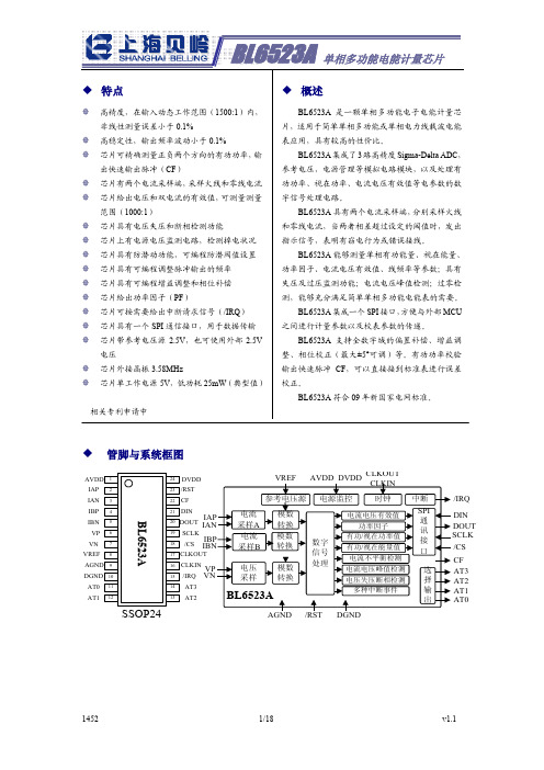

© Semiconductor Components Industries, LLC, 2006 March, 2006 − Rev. 31Publication Order Number:MPS6560/DMPS6560Audio TransistorNPN SiliconFeatures•Pb−Free Package is Available*MAXIMUM RATINGSRating Symbol Value Unit Collector−Emitter Voltage V CEO25Vdc Collector−Base Voltage V CBO25Vdc Emitter−Base Voltage V EBO 5.0Vdc Collector Current − Continuous I C500mAdcTotal Device Dissipation @ T A = 25°C Derate above 25°C P D6255.0WmW/°CTotal Device Dissipation @ T C = 25°C Derate above 25°C P D 1.512WmW/°COperating and Storage JunctionTemperature RangeT J, T stg−55 to +150°C THERMAL CHARACTERISTICSCharacteristic Symbol MaxUnit Thermal Resistance, Junction−to−Ambient(Note 1)R q JA200°C/W Thermal Resistance, Junction−to−Case R q JC83.3°C/WStresses exceeding Maximum Ratings may damage the device. Maximum Ratings are stress ratings only. Functional operation above the Recommended Operating Conditions is not implied. Extended exposure to stresses above the Recommended Operating Conditions may affect device reliability.1.R q JA is measured with the device soldered into a typical printed circuit board.*For additional information on our Pb−Free strategy and soldering details, please download the ON Semiconductor Soldering and Mounting Techniques Reference Manual, SOLDERRM/D.†For information on tape and reel specifications, including part orientation and tape sizes, please refer to our T ape and Reel Packaging Specifications Brochure, BRD8011/D.Device Package Shipping†MPS6560TO−925,000 Units/Box MPS6560G TO−92(Pb−Free)5,000 Units/Box ORDERING INFORMATION2ELECTRICAL CHARACTERISTICS (T A = 25°C unless otherwise noted)CharacteristicSymbolMinMaxUnitOFF CHARACTERISTICSCollector −Emitter Breakdown Voltage (Note 2)(I C = 10 mAdc, I B = 0)V (BR)CEO 25−Vdc Collector −Base Breakdown Voltage (I C = 100 m Adc, I E = 0)V (BR)CBO 25−Vdc Emitter −Base Breakdown Voltage (I E = 100 m Adc, I C = 0)V (BR)EBO 5.0−Vdc Collector Cutoff Current (V CE = 25 Vdc, I B = 0)I CES −100nAdc Collector Cutoff Current (V CB = 20 Vdc, I E = 0)I CBO −100nAdc Emitter Cutoff Current(V EB(off) = 4.0 Vdc, I C = 0)I EBO−100nAdcON CHARACTERISTICS (Note 2)DC Current Gain(I C = 10 mAdc, V CE = 1.0 Vdc)(I C = 100 mAdc, V CE = 1.0 Vdc)(I C = 500 mAdc, V CE = 1.0 Vdc)h FE355050−−200−Collector −Emitter Saturation Voltage (I C = 500 mAdc, I B = 50 mAdc)V CE(sat)−0.5Vdc Base −Emitter On Voltage(I C = 500 mAdc, V CE = 1.0 Vdc)V BE(on)−1.2Vdc SMALL−SIGNAL CHARACTERISTICS Current−Gain — Bandwidth Product(I C = 10 mAdc, V CE = 10 Vdc, f = 20 MHz)f T 60−MHz Output Capacitance(V CB = 10 Vdc, I E = 0, f = 1.0 MHz)C obo−30pF2.Pulse Test: Pulse Width v 300 m s; Duty Cycle v 2.0%.PACKAGE DIMENSIONSNOTES:1.DIMENSIONING AND TOLERANCING PER ANSI Y14.5M, 1982.2.CONTROLLING DIMENSION: INCH.3.CONTOUR OF PACKAGE BEYOND DIMENSION R IS UNCONTROLLED.4.LEAD DIMENSION IS UNCONTROLLED IN P AND BEYOND DIMENSION K MINIMUM.PLANEDIM MIN MAX MIN MAX MILLIMETERSINCHES A 0.1750.205 4.45 5.20B 0.1700.210 4.32 5.33C 0.1250.165 3.18 4.19D 0.0160.0210.4070.533G 0.0450.055 1.15 1.39H 0.0950.105 2.42 2.66J 0.0150.0200.390.50K 0.500−−−12.70−−−L 0.250−−− 6.35−−−N 0.0800.105 2.04 2.66P −−−0.100−−− 2.54R 0.115−−− 2.93−−−V0.135−−−3.43−−−TO−92 (TO−226)CASE 29−11ISSUE ALSTYLE 1:PIN 1.EMITTER2.BASE3.COLLECTORON Semiconductor and are registered trademarks of Semiconductor Components Industries, LLC (SCILLC). SCILLC reserves the right to make changes without further notice to any products herein. SCILLC makes no warranty, representation or guarantee regarding the suitability of its products for any particular purpose, nor does SCILLC assume any liability arising out of the application or use of any product or circuit, and specifically disclaims any and all liability, including without limitation special, consequential or incidental damages.“Typical” parameters which may be provided in SCILLC data sheets and/or specifications can and do vary in different applications and actual performance may vary over time. All operating parameters, including “Typicals” must be validated for each customer application by customer’s technical experts. SCILLC does not convey any license under its patent rights nor the rights of others. SCILLC products are not designed, intended, or authorized for use as components in systems intended for surgical implant into the body, or other applications intended to support or sustain life, or for any other application in which the failure of the SCILLC product could create a situation where personal injury or death may occur. Should Buyer purchase or use SCILLC products for any such unintended or unauthorized application, Buyer shall indemnify and hold SCILLC and its officers, employees, subsidiaries, affiliates,and distributors harmless against all claims, costs, damages, and expenses, and reasonable attorney fees arising out of, directly or indirectly, any claim of personal injury or death associated with such unintended or unauthorized use, even if such claim alleges that SCILLC was negligent regarding the design or manufacture of the part. SCILLC is an Equal Opportunity/Affirmative Action Employer. This literature is subject to all applicable copyright laws and is not for resale in any manner.PUBLICATION ORDERING INFORMATION分销商库存信息: ONSEMIMPS6560G。

基於L6563的PFC前置稳压器L6563是意法半导体公司2005年底推出的一个新型过渡工作模式功率因数校正(PFC)前置稳压控制器IC。
L6563基於标准的TM PFC(过渡功率因数校正器)内核,通过增加几个无源器件就可以新增多个辅助功能,而这些功能通常需要增加复杂电路才能实现。
本文介绍了基於L6563的PFC前置稳压器典型应用。
功率因素是有效功率与总耗电量(视在功率)之间的关系,也就是有效功率除以总耗电量(视在功率)的比值。
基本上功率因素可以衡量电力被有效利用的程度,当功率因素值越大,代表其电力利用率越高。
开关电源上的功率因素校正器的运作原理是去控制调整交流电电流输入的时间与波型, 使其与直流电电压波型尽可能一致,让功率因素趋近於1。
这对於电力需求量大到某一个水准的电子设备而言是很重要的, 否则电力设备系统消耗的电力可能超出其规格,极可能干扰铜系统的其他电子设备。
一般状况下, 电子设备没有功率因素校正(Power Factor Correction, PFC)时其PF值只有大约0.5。
图1. 双级有源功率因数校正开关电源典型电路一、有源功率因数校正功率因数校正技术有两种,即有源(Active PFC)和无源(Passive PFC)。
其中,无源PFC 使用由电感、电容等组合而成的电路来降低谐波电流,其输入电流为低频的50Hz到60Hz,因此需要大量的电感与电容,而且其功率因素校正仅达75%~80%。
有源PFC使用有源元件控制线路及功率型开关元件(power sine conductor On/Off switch),基本运作原理为调整输入电流波型使其与输入电压波形尽可能相似,功率因素校正值可达近乎100%。
相对地,因为其优异功能,有源PFC价格也较高。
此外,有源PFC有另一项重要附加价值,即电源供应器输入电压范围可扩增为90Vdc到264Vdc的全域电压,电源供应器不需切换电压。
图2. 输入电压前馈功能的内部框图有源功率因数校正是目前开关电源(switch-mode power supply,SMPS)应用中的一种常见功能,特别是用於抑制公共供电系统中的谐波电流的稳压应用,例如欧洲的EN61000-3-2和日本的EIDA-MITI标准。


BROSA GmbHDr. Klein Straße 1D-88069 TettnangPhone: +49(0)7542 93 35 0Fax: +49(0)7542 93 35 35**************BROSA Pte Ltd 25 Lorong Kilat #02-01 Singapore 598126 Phone: +65 6795 2324 Fax: +65 6795 2428 *****************BROSA B.V. Galliershof 38 NL - 5349 BV Oss, Holland Phone: +31 412 6146 02 Fax: +31 412 6146 86 *************BROSA (Nanjing) Co., Ltd. Jinma Lu 3, Maqun Scientific Park, Qixia District 210049 Nanjing Phone: +86 (25)8222 4639 Fax: +86 (25)8222 4639 ***************** ................................................................................................................................................................ ................................................................................................................................................................ © 2022 BROSA GmbH, Tettnang, GermanyOperating ManualBROSA Tension Load Cell Type 0111, 0113English translation of German original operating manualVersion: 01/2022BROSA Tension Load Cell© 2022 BROSA GmbH, Tettnang, Germany English translation of the original2 / 12............................................................................................................................................................... ........................................................................................................................................................................................................................................................................................................................... ............................................................................................................................................................Content1General information ................................................................................................ 3 1.1Safety instructions – Explanation of symbols: .................................................... 3 2 Description of the BROSA tension load cell ............................................................. 4 2.1Structure and functionality ................................................................................ 4 2.2Information on explosion protection .................................................................. 6 3Advice on the safe handling of BROSA force measuring sensors ............................. 6 3.1Handling .......................................................................................................... 7 3.2 Installation and commissioning . (7)3.2.1 General information (7)3.2.2Additional information for operation in areas subject to explosion hazards (8)3.2.2.1Intrinsically safe sensors ..................................................................... 9 3.3 Operation and maintenance ........................................................................... 10 3.3.1Operation ................................................................................................ 10 3.3.2Maintenance ........................................................................................... 11 3.4Disassembly .................................................................................................. 11 3.5 Disposal .. (12)© 2022 BROSA GmbH, Tettnang, GermanyEnglish translation of the original3 / 12BROSA Tension Load Cell............................................................................................................................................................... ............................................................................................................................................................... ............................................................................................................................................................ ............................................................................................................................................................ ............................................................................................................................................................ ............................................................................................................................................................ 1 General informationRead the operating instructions and the product-specific documents carefully beforecommissioning the sensor.Make sure that the sensor is fully suitable for the applications in question.Improper use or any use other than intended may result in a malfunction of the sensor orundesirable effects in your application. For this reason, installation, electrical connection,commissioning and maintenance of the sensor may only be carried out by trainedpersonnel authorized by the plant operator.We also expressly point out that any liability is excluded if instructions in this documentationare disregarded.Current certificates can be downloaded from the BROSA GmbH website.Only the German version of this operating manual represents the original document.1.1 Safety instructions – Explanation of symbols:WARNING! This symbol indicates dangers that can lead to personal injury andproperty damage!BROSA Tension Load Cell© 2022 BROSA GmbH, Tettnang, Germany English translation of the original4 / 12............................................................................................................................................................... ........................................................................................................................................................................................................................................................................................................................... ............................................................................................................................................................ 2 Description of the BROSA tension load cell2.1 Structure and functionalityThe BROSA type 0111 and 0113 tension load cells transmit and measure the tensile and/orcompressive force between two pins, which are connected by the tension load cell.Figure 1 shows the typical layout: Fig. 1: Tension load cellThe tension load cell consists of a rectangular measuring body that absorbs the load (1), theends of which have holes (1a) for mounting connecting pins. By default, the bore axes areparallel, special designs with holes arranged at an angle to each other (e.g., 90°) arepossible. Fork ends (single- or double-sided) are available. In some cases, there is aconnection support (2) firmly connected to the measuring body, on which - if not placeddirectly on the measuring body - the necessary elements for the electrical connection (plug orcable, 3) are attached and which - if not placed in the measuring body - contains themeasurement electronics.Optionally, the measuring body can contain elements to lubricate the bearing (1b). The Ex dtype 0113 tension load cell is always equipped with a threaded pin (4) for electrical potentialequalisation (optional in the other types). On special request, the holes can be provided withplain or spherical bearings. BROSA tension load cells are by default equipped with a surfacecoating (primer or paint for use in continental or maritime environments); by special order,tension load cells made of stainless steel are available.1a4© 2022 BROSA GmbH, Tettnang, GermanyEnglish translation of the original5 / 12BROSA Tension Load Cell............................................................................................................................................................... ............................................................................................................................................................... ............................................................................................................................................................ ............................................................................................................................................................ ............................................................................................................................................................ ............................................................................................................................................................ The use below the water surface is generally possible after testing and approval by BROSA,special requirements are the used materials and surface coatings, the tightness and theelectrical connections.In addition, there is the possibility that the water pressure impacts the measurement result.Figure 2: Installation conditionsThe tension load cell (1) is connected to the adjacent components with bolts (2). Force Ftransmitted from the connection is transmitted to the measuring electronics through analysisof the resulting deformation of the measuring body and output as an electric signal. Versionswith two measuring systems, either with output signals on separate connectors/cables orcombined in one connector/cable, are available as options. More information can be found inthe technical datasheets, which may be obtained free of charge from BROSA. 12BROSA Tension Load Cell© 2022 BROSA GmbH, Tettnang, Germany English translation of the original6 / 12............................................................................................................................................................... ........................................................................................................................................................................................................................................................................................................................... ............................................................................................................................................................ 2.2 Information on explosion protectionThe BROSA type 0111 tension load cells are optionally available in an intrinsically safe design for use in potentially explosive atmospheres. Actual certificates can bedownloaded on BROSA Homepage.Use of intrinsically safe tension load cells in zone 0 is not allowed.The Ex d type 0113 tension load cell is designed to be pressure-resistant and is therefore suitable for use in potentially explosive atmospheres. Actual certificates can bedownloaded on BROSA Homepage.WARNING! Use of the Ex d tension load cell in zone 0 is not allowed.Current certificates can be downloaded from the BROSA GmbH website.3 Advice on the safe handling of BROSA forcemeasuring sensorsWARNING! Non-compliance with the following instructions can lead to sensor damage and/or impairment of measurement results. The analysis of an erroneous measurement can result in personal injury or material damage.WARNING! Despite their sturdy design, BROSA force measuring sensors may not be used for any other than the intended purpose (see. Section 1.1). With improper use, dangers to life and limb of the user or third parties and/or impairment of the device in which the force measuring sensor is implemented or other material assets can be caused.© 2022 BROSA GmbH, Tettnang, GermanyEnglish translation of the original7 / 12BROSA Tension Load Cell............................................................................................................................................................... ............................................................................................................................................................... ............................................................................................................................................................ ............................................................................................................................................................ ............................................................................................................................................................ ............................................................................................................................................................ 3.1 HandlingWARNING! BROSA sensors contain high-quality measurement electronics. Make sure they are handled carefully.- BROSA force measuring sensors are delivered in transport-safe packaging. Werecommend that you remove the sensors from the package immediately prior toinstallation.- The mass of the force measuring sensor is to be observed when selectingappropriate handling equipment and/or lifting gear.- BROSA force measuring sensors must be secured against falling. Do not throwsensors!- Use as a tool (e.g., impact, slotting or lever tool) is not permitted; it can causedamage to the sensor and thus falsify the measurement results.3.2 Installation and commissioning3.2.1 General informationWe recommend taking the following actions in the given order using the “four -eyeprinciple”.a) Checking the sensor-measuring point assignment: It must be ensured that thesensor to be installed is designed for use at the intended measuring point.For this purpose, check information on the technical datasheet and thenameplate, in particular the item or the identification number and themeasuring range, against the data of the measuring point.WARNING! A sensor not designed for the particular measuring point must not beinstalled.b) Inspection of the sensor for intactness and function: It must be ensured that the sensor to be incorporated is free of damage of any kind.BROSA Tension Load Cell© 2022 BROSA GmbH, Tettnang, Germany English translation of the original8 / 12............................................................................................................................................................... ........................................................................................................................................................................................................................................................................................................................... ............................................................................................................................................................ WARNING! A damaged sensor must not be installed!c) Installation of the sensor in the measuring point:The force measuring sensor is to be installed according to the offer drawingand is to be aligned on the intended contact surface.WARNING! The force measuring sensor must not be driven in or aligned usingimpact tools!After alignment, which may be necessary depending on the sensor type, the forcemeasuring sensor must be secured against movement and rotation using the elements provided for this purpose. Attention must be paid to the correct alignment of the force measuring sensor to the intended measuring direction (see direction marks).WARNING! A misaligned sensor leads to erroneous measurement results!d) Establishment of electrical connection: The elements on the sensor for theelectrical connection are to be connected to the power supply, the earthconnection if necessary, and the evaluation system of the device. In doing so,the information given on the nameplate for plug or cable assignment and, ifapplicable the installation guidelines of the cable, are to be observed.WARNING! An incorrect or incomplete electrical connection impairs or preventsmeasurement.e) Functional check: After completed mechanical (see c) and electric (see d)installation, load on the sensor is to be applied over the entire measuringrange; the output measurement signals are to be subjected to a plausibilitycheck.WARNING! If due to unusual events (e.g., deformation or unusual noise), measure-ment results are considered implausible or there is suspicion that the sensor is malfunc-tioning for any other reason, it must not be put into operation.3.2.2 Additional information for operation in areas subject to explosion hazards Only those sensors with the corresponding labels are approved for use in areassubject to explosion hazards.© 2022 BROSA GmbH, Tettnang, GermanyEnglish translation of the original9 / 12BROSA Tension Load Cell............................................................................................................................................................... ............................................................................................................................................................... ............................................................................................................................................................ ............................................................................................................................................................ ............................................................................................................................................................ ............................................................................................................................................................ If the open cable end is connected inside an area subject to explosion hazards, the connection must be inside a terminal box/switching cabinet certified in accordance with the ATEX-directive. If it is connected outside an area subject to explosion hazards, it must be in line with the general requirements for electrical equipment.When using intrinsically safe (Ex-i) sensors, the use of an Ex-i isolator is mandatory to limit the energy supplied to the hazardous area and to provide galvanic isolation from all other non-intrinsically safe circuits.3.2.2.1 Intrinsically safe sensorsSensors using ExDANGmicro2W*** amplifiers are to be installed according to the following specifications:Figure 6: Connection example Ex i sensor with Ex DANGmirco2W*** amplifierThe supply and the measuring signal are fed into the hazardous area via an isolation amplifier. Isolation amplifiers from other manufacturers can also be used if they meet the safety-related limit values.During installation, the distinction with regard to the insulation strength of the strain gauge resistance bridge against the sensor spring body must be observed. The amplifier type ExDANGmicro2W_A** is to be regarded as separate from the spring body. TheBROSA Tension Load Cell© 2022 BROSA GmbH, Tettnang, Germany English translation of the original10 / 12............................................................................................................................................................... ........................................................................................................................................................................................................................................................................................................................... ............................................................................................................................................................ amplifier type ExDANGmicro2W_B** is to be regarded as connected to the spring body in the event of a fault.The routing of the connection cable for amplifier type ExDANGmicro2W_*B2 and type ExDANGmicro2W_*B4 requires protection against damage and tensile stress, ensured by a suitable device.The complete list of possible amplifier configurations can be found in the certificate.3.3 Operation and maintenance3.3.1 OperationBROSA force measuring sensors operate automatically; attaching tools is not required for operation. Direct manual intervention by the operator is not necessary; there aretherefore no requirements for the operator to wear protective equipment during operation. However, the relevant requirements for the device in which the force measuring sensor is implemented must be observed.BROSA force measuring sensors emit neither airborne acoustic noise nor electro-magnetic radiation.Operation of BROSA force measuring sensors is permitted only within the parameters and properties given in the technical datasheets and on the nameplate.These are, among others:-Measuring range -Temperature range -Permissible supply voltage -Electrical protection class - MaterialIt must be ensured that no parasitic influences such as forces transverse to themeasuring direction are transmitted via the force measuring sensor.Inductive or capacitive coupling with the connection cable(s) of the sensor can distort the measurement result and must be avoided. Some examples of these kinds of couplings can be caused e.g., by unfavourable cable routing (parallel power lines, frequencyconverters, transformers, motors, incorrect grounding/shielding and the like).© 2022 BROSA GmbH, Tettnang, GermanyEnglish translation of the original11 / 12BROSA Tension Load Cell............................................................................................................................................................... ............................................................................................................................................................... ............................................................................................................................................................ ............................................................................................................................................................ ............................................................................................................................................................ ............................................................................................................................................................ When performing electric welding in the vicinity of the sensor, all connections must be disconnected and isolated. It must be ensured that no welding current is flowing through the sensor.WARNING! Operation outside the specified parameters or contrary to existing properties or improper use can damage the sensor and cause it to fail or lead to faulty measuring results. If the sensor is overloaded, this can lead to the whole machine being equally overloaded and possibly endangering its stability.3.3.2 MaintenanceIn its capacity as a sensor, BROSA force measuring sensors are maintenance-free. As load-transmitting elements, however, they are subject to mechanical stress, requiring regular inspections of the fault-free state of each force measuring sensor. The intervals between inspections depend on the intensity of use and must be determined by the end-user. Additional lubrication holes are not necessary for the sensor to function, but are used to lubricate secondary components, so the end-user is responsible for the lubrication cycles.An inspection includes the following points:-Visual inspection for damage to the measuring body and wiring as well as contamination. - Function test/plausibility checkThe causes of existing errors are to be identified and remedied. If the test indicates an improper sensor state, it must be taken out of operation. If a malfunction or damage is detected on the sensor, it must be sent to the manufacturer's factory for diagnosis and, if necessary, repaired.WARNING! The sensor may only be repaired at the factory. Intervention (e.g., opening, mechanical processing and the like) done by parties other than the manufacturer means the safe operation of the sensor is no longer ensured and voids the warranty.3.4 DisassemblyWe recommend performing the following actions in the order given.a)Establishment of a load-free state at the measuring point: The force measuring sensor is to be unloaded before removal.BROSA Tension Load Cell© 2022 BROSA GmbH, Tettnang, Germany English translation of the original12 / 12............................................................................................................................................................... ........................................................................................................................................................................................................................................................................................................................... ............................................................................................................................................................ WARNING! Removal of a force measuring sensor under load poses seriousdangers to the life and limb of bystanders and can cause major damage.This is therefore not permitted.b)Undoing the electrical connection c)Remove the mechanical securing elements d) Remove the force measuring sensorWARNING! If the force measuring sensor is to be reused, it must not be removedusing impact tools!3.5 DisposalIf the end of the service life is reached, the force measuring sensor is to be disposed of in an environmentally friendly way. Since the non-metallic components are a smallproportion compared to the mass of the force measuring sensor, it can be recycled as a whole as scrap steel.If the sensor is stored before final disposal, an appropriate storage location is to beselected which prevents harmful substances from entering the environment. If necessary, the sensor must be cleaned.WARNING! BROSA force measuring sensors contain traces of environmentallyhazardous substances. This is also true of the impurities created during use.Contamination of the environment by these substances is to be prevented.。
©On-Bright Electronics Confidential DESCRIPTIONSOB6563 is an active transition-mode (TM) power factor correction (PFC) controller for AC-DC switching mode power supply applications.OB6563 features an internal start-up timer for stand-alone applications, a one quadrant multiplier with THD optimizer for near unity power factor, zero current detector (ZCD) to ensure TM operation, a current sensing comparator with built-in leading-edge blanking, and a totem pole output ideally suited for driving a power MOSFET.OB6563 offers great protection coverage including system over-voltage protection (OVP) to eliminate runaway output voltage due to load removal, VCC under voltage lockout (UVLO), cycle-by-cycle current limiting, multiplier output clamping that limit maximum peak switch current, and gate drive output clamping for external power MOSFET protection.With added system open loop protection feature, OB6563 shuts down system when the feedback loop is open.In OB6563, the dynamic OVP sensing current is set to 10uA, which will decrease system standby power greatly. When used with On-Bright PWM controller OB2298 or Quasi-Resonant controller OB2203 in a 150W AC/DC power design, it can deliver <0.4W standby power at universal AC range input.OB6563 is offered in SOP-8 and DIP-8 packages.FEATURES• Transition Mode (TM) Operation• One quadrant multiplier with THD optimizer • Low Dynamic OVP Sensing Current Setting • Low Start-up Current and Operating Current • Cycle-by-Cycle Current Limiting • Internal RC Filter• Trimmed 1.5% Internal Bandgap Reference • Under Voltage Lockout with Hysteresis• Dynamic and Static Output Over-Voltage Protection (OVP)• Internal Start-up Timer for Stand-alone Applications • Disable Function• Totem Pole Output with High State Clamping • System Open Loop Protection• Proprietary Audio Noise Free Operation • 9.5V to 28V wide range of VCC voltageAPPLICATIONS• Electronic Ballast • AC-DC SMPSTYPICAL APPLICATIONGD CSVCC 12348765ZCD MULT COMP INV ACGND OB6563C1C2C3R1C4C5R2R3R4R5Q1D1L1C6R6D2D3R7R8++On -B ri g ht Co nf i de nt i a l toH i gh ra y©On-Bright Electronics Confidential GENERAL INFORMATIONTerminal Assignment In SOP8 or DIP8 Package.Ordering Information Part Number Description OB6563AP 8 Pin DIP, Pb free in Tube OB6563CP 8 Pin SOP, Pb free in Tube OB6563CPA 8 Pin SOP, Pb free in T&RPackage Dissipation RatingPackageR θJA ( C/W) DIP8 90 SOP8 150Absolute Maximum Ratings Symbol Parameter Value VCC DC Supply voltage30 V I_ZCDZero CurrentDetector Max.Current50mA(source)-10mA(sink)CS INV COMP MULTAnalog inputs & outputs-0.3 to 7V Tj Min/Max Operating Junction Temperature-40 to 150 oC TstgMin/Max StorageTemperature-55 to 150 oCLead Temperature (Soldering, 10secs ) 260 oCNote: Stresses beyond those listed under “absolute maximumratings” may cause permanent damage to the device. These are stress ratings only, functional operation of the device at these or any other conditions beyond those indicated under “recommended operating conditions” is not implied. Exposure to absolute maximum-rated conditions for extended periods may affect device reliability.12348765INVCOMP MULTCS VCC GD GND ZCD On -B ri g ht Co nf de nt i a l t oH i gh ra y©On-Bright Electronics Confidential Marking InformationTERMINAL DESCRIPTIONSPin Num Pin Name I/O Description 1 INV I Inverting Input of Error Amplifier. Connected to Resistor Divider fromSystem Output. This pin is also used for system open loop protection.2 COMP O Output of Error Amplifier. A feedback compensation network is placedbetween COMP and the INV pin.3 MULT I Input of Multiplier. Connected to Line Voltage after Bridge Diodes via AResistor Divider to Provide Sinusoidal Reference Voltage to the Current Loop.4 CS I Current Sense Input Pin. Connected to MOSFET Current Sensing Node.5 ZCD I Zero Current Detection Input. When Activated, A New Switching CycleStarts. If it is connected to GND, the device is disabled.6 GND P Ground Pin7 GD O Gate driver output. Drive Power MOSFET.8 VCC P DC Supply Voltage.On -B ri g ht Co nf i de nt i a l toH igh r a y©On-Bright Electronics Confidential BLOCK DIAGRAMOn -B ri g ht Co nf i de nt i a l toH i gh r a y©On-Bright Electronics Confidential ELECTRICAL CHARACTERISTICS(T A = 25O C if not otherwise noted)Symbol Pin Parameter Test Conditions Min Typ Max Unit SUPPLY VOLTAGE SECTION Vcc 8 Operating Range After Turn On 11 28 V8 Turn-on Threshold 11 12 13 VUVLO8 Turn-off Threshold 8.5 9.5 10.5 VHys 8 Hysteresis 2.5 V Vz 8 Zener Voltage Icc =5mA 30 33 36 V SUPPLY CURRENT SECTION Icc-start 8 Start-up Current Vcc =11V 35 70 uA Iq 8 Quiescent Current, NoSwitchingVcc =14.5V 2.9 4 mAC L =1nf @ 70kHz 4 5.5 mAIcc 8 Operating Supply Current In OVP condition Vpin1=2.7V1.42.1 mA Vpin5≤150mV Vcc=14.5V1.12.1 mAIq 8 Quiescent Current Vpin5≤150mV, Vcc<Vcc off35 70 uA ERROR AMPLIFIER SECTIONVinv 1 Voltage Feedback InputThresholdV cc =14.5V 2.45 2.5 2.55 VVinv 1 Line Regulation 12V<Vcc<28V 2 5 mV Iinv 1 Input Bias Current I DD = 10 mA -0.1 -1 uA Gv Voltage Gain Open Loop 60 80 dB Gb Gain Bandwidth 1.2 MHzSource Current Vcomp=3.6V, Vinv=2.4V -1 -3 -5 mAIcomp 2Sink Current Vcomp = 3.6V, Vinv = 2.6V 1 3 5 mA Upper Clamp Voltage Isource=0.5mA 4.9 VVcomp 2Lower Clamp Voltage Isink=0.2mA 2.25 V MULTIPLIER SECTION Vmult 3 Linear Operating Range Vcomp=3.0V 0 to3.5VΔVcs/ ΔVmult Output Max. Slope Vmult=from 0 to 0.5v Vcomp=Upper ClampVoltage1.65 1.9 V/V K Gain Vmult =1V, Vcomp = 3.5V 0.65 1/V CURRENT SENSE COMPARATOR Vcs 4 Current Sense Reference Clamp Vmult=2.5V Vcomp=Upper ClampVoltage1.55 1.7 1.85 VIcs 4 Input Bias Current Vcs=0 0.1 uA Td(H-L) 4 Delay to Output 200 450 ns On -B ri g ht Co nf i de nt i a l toH i gh r a y©On-Bright Electronics Confidential ELECTRICAL CHARACTERISTICS (Continued)(T A = 25O C if not otherwise noted)Symbol Pin Parameter Test Conditions Min Typ Max Unit ZERO CURRENT DETECTOR Input Threshold Voltage Rising Edge1.9VVzcd 5 Hysteresis 0.3 0.5 0.7 VVzcd 5 Upper Clamp Voltage Izcd=2.5mA 5.1 5.7 6.3 V Vzcd 5 Lower Clamp Voltage Izcd =-2.5mA 0.4 0.65 0.8 V Izcd 5 Input Bias Current 1V ≤Vzcd ≤4.5V 2 uA Izcd 5 Source Current Capability -3 -5 mA Izcd 5 Sink Current Capability 3 10 mA Vdis 5 Disable Threshold 150250 350mV Izcd 5 Restart Current After Disable Vzcd<VdisVcc>Vccoff-100 -200 -400 uAGATE DRIVE SECTION VoL 7 Low Output Voltage Vcc=14.5V, Io=100mA 1.5 V VoH 7 High Output Voltage Vcc=14.5V, Io=100mA 8 V Tr 7 Rising Time Cl =1000pF, 10~90% 80 150ns Tf 7 Falling Time Cl =1000pF, 10~90% 30 70 ns Voclamp 7 Output ClampVoltage Vcc =28V 16 18 V OUTPUT OVER VOLTAGE SECTION Iovp 2 Dynamic OVP Triggering Current8 10 12 uAStatic OVP Threshold 2.1 2.25 2.4 V STARTUP TIMER Tstart Re-Start Timer Period 70 150 300 us SYSTEM OPEN LOOP PROTECTION COMPARATOR Vth_ol System Open Loop Protection Comparator Threshold250 mVOn -B ri g ht Co nf i de nt i a l toH i gh r a y©On-Bright Electronics Confidential TYPICAL PERFOMANCE CHARTOperating Current vs Supply Voltage3.03.54.04.55.05.51015202530VCC(V)I c c (m A )Quiescent Current vs VCC1234051015202530VCC(V)I q (m A )Operating Current vs Temperature4.04.24.44.64.85.0-20104070100130Temperature(℃)I c c (m A )UVLO vs Temperature8910111213-20104070100130Temperature(℃)U V L O (V )Reference Voltage vs Temperature2.402.452.502.552.60-20104070100130Temperature(℃)V i n v (V )Multiplier Gain vs Temperature0.40.50.60.70.8-20104070100130Temperature(℃)K (1/V )On -B ri g ht Co nf i de nt i a l toH i gh r a y©On-Bright Electronics ConfidentialCurrent Sense Threshold Clamping vsTemperature1.41.51.61.71.8-20104070100130Temperature(℃)V C S (V )Startup Current vs Temperature20253035404550-20104070100130Temperature(℃)I s t a r t u p (u A )Gate Driver Clamping vs Temperature1415161718-20104070100130Temperature(℃)V g a t e _m a x (V )Restart Timer Period vs Temperature100120140160180-20104070100130Temperature(℃)T _w a t c h d o g (u s )Multiplier Characterization0.00.20.40.60.81.01.21.41.61.82.00.00.51.01.52.02.53.03.54.04.5Vmult(V)M u l t i p l i e r O u t p u t (V )COMP=2.8V COMP=3.0V COMP=3.2V COMP=3.5V COMP=4.0V COMP=4.5V COMP=5.0VDynamic OVP Triggering Current(uA)vsTemperature89101112-20104070 100130Temperature(℃ )On -B ri g ht Co nf i de nt i a l toH i gh r a y©On-Bright Electronics ConfidentialOPERATIONAL DESCRIPTIONOB6563 is a highly integrated power factor correction (PFC) controller IC. The transition mode control greatly reduces the switch turn-on loss, improves the conversion efficiency and provides very good power factor correction.• Error AmplifierConnected to a resistor divider from output line, the inverting input of the Error Amplifier (E/A) is compared to an internal reference voltage(2.5V) to set the regulation on output voltage.The E/A output is internally connected to the multiplier input and externally connected for loop compensation. It is usually realized with a capacitor which connected between the inverting input and EA output. The system loop bandwidth is set below 20 Hz to suppress the AC ripple of the line voltage.• MultiplierThe one quadrant multiplier output limits the MOSFET peak current with respect of the system output voltage and the AC half wave rectified input voltage. Through controlling the CS comparator threshold as the AC line voltage traverses sinusoidally from zero to peak line voltage, the PFC preconverter’s load appears to be resistive to the AC line.In OB6563, the two inputs for the multiplier are designed to achieve good linearity over a wide dynamic range to represent an AC line free from distortion. Special efforts have been made to assure universal line applications with respect to a 90 to 264 VAC range.The multiplier output is internally clamped to 1.7V. So the MOSFET is protected against critical operation during start up.• Over Voltage ProtectionLimited by low loop bandwidth setting, detection of output OVP could become very slow in regular approach. OB6563 offers two level OVP protection including dynamic OVP for output fast transient protection and static OVP for output stead-state protection.In an output transient OVP event, current in proportion to ΔV flows into Error Amplifier output COMP through compensation network. When this current reaches 8uA, the output of multiplier is forced to decrease and on-time of MOSFET is reduced. When current continues to exceed 10uA, the power MOSFET is turned off until the current falls below ~2.5uA. In this way, the system output cannot reach to a very high value.When OVP event lasts long enough, the Error Amplifier Output, COMP, will saturate and stay low. Static OVP comparator is activated and power MOSFET Gate is off when COMP voltage is dropped below 2.25V. Normal operation is resumed when Error Amplifier goes back to its linear region after output voltage drops.Over-voltage protection block• Startup Current and Start up ControlThe typical startup current of OB6563 is 35uA when the VCC pin is lower than the UVLO threshold so that VCC could be charged up and start up the device. A high value, low wattage startup resistor can therefore be used to minimize the power loss during the normal operation.• Current Sensing Comparator and Leading EdgeBlankingCycle-by-cycle current limiting is provided in OB6563’s peak current mode control. The switch current is detected by a sense resistor into the sense pin. The multiplier output voltage is compared with this sense voltage through an internal comparator. An internal RC filter is connected at the CS pin which smoothes the switch-on current spike. The remaining switch-on spike is blanked out via an internal leading edge blanking (LEB) circuit. Another extra function of LEB is that it limits the system minimum on time, thus the THD of system at light load will be decreased.The RS flip-flop ensures that only one single switch-on and switch-off pulse appears at the gate drive output during a given cycle.• Zero Current DetectionOn -B ri g ht Co nf i de nt i a l toH i gh r a y©On-Bright Electronics Confidential OB6563 can perform zero current detection by using an auxiliary winding of the inductor. When the stored energy is fully released to the output, the voltage at ZCD decrease. A new switching cycle is initiated following the ZCD triggering. The turn on of power MOSFET is initiated at moment that the inductor’s current reaches zero.• Disable FunctionWhen the ZCD pin is pulled low, OB6563 is disabled and some internal functional blocks are turned off. The operation current is very small under this condition until the ZCD pin is released.• Gate Drive OutputThe output stage is designed to ensure zero cross-conduction current. This minimizes heat dissipation, increase efficiency, and enhance reliability. The output driver is also slew rate controlled to minimize EMI. Thebuilt-in 16V clamp at the gate output protects the MOSFET gate from high voltage stress.• Protection ControlsOB6563 ensures good reliability design through its good protection coverage. Output dynamic and static over-voltage protection (OVP), VCC under voltage lockout (UVLO), cycle-by-cycle current limiting and output gate clamp are standard features provided by OB6563.• System Open Loop ProtectionA new function of system open loop protection is provided in OB6563. The voltage at INV pin is sensed. If INV pin is below 0.25V typical, the switching will be stopped. In this way, the system output voltage cannot increase too high (only the rectified line voltage), and the pre-converter will be protected from damage.On -B ri g ht Co nf i de nt i a l toH i gh r a y©On-Bright Electronics Confidential PACKAGE MECHANICAL DATA8-Pin Plastic DIP Dimensions In Millimeters Dimensions In InchesSymbol Min Max Min MaxA 3.710 4.310 0.146 0.170 A1 0.500 0.020 A2 3.200 3.600 0.126 0.142B 0.350 0.650 0.014 0.026 B1 1.524 (BSC) 0.060 (BSC)C 0.200 0.360 0.008 0.014D 9.000 9.500 0.354 0.374E 6.200 6.600 0.244 0.260 E1 7.320 7.920 0.288 0.312 e 2.540 (BSC) 0.100 (BSC) L 3.000 3.600 0.118 0.142 E2 8.200 9.000 0.323 0.354 O n -B r i g h t C o n f i d e n t i a l to H i g h r a y©On-Bright Electronics Confidential 8-Pin Plastic SOPDimensions In Millimeters Dimensions In InchesSymbol Min Max Min MaxA 1.350 1.750 0.053 0.069 A1 0.100 0.250 0.004 0.010 A2 1.300 1.550 0.051 0.061 b 0.330 0.510 0.013 0.020c 0.170 0.250 0.006 0.010D 4.700 5.150 0.185 0.203E 3.800 4.000 0.150 0.157 E1 5.800 6.200 0.228 0.244 e 1.270 (BSC) 0.050 (BSC)L 0.400 1.270 0.016 0.050 θ 0º 8º 0º 8ºO n -B r i g h t C o n f i d e n t i a l to H i g h r a y©On-Bright Electronics Confidential IMPORTANT NOTICERIGHT TO MAKE CHANGES On-Bright Electronics Corp. reserves the right to make corrections, modifications, enhancements, improvements and other changes to its products and services at any time and to discontinue any product or service without notice. Customers should obtain the latest relevant information before placing orders and should verify that such information is current and complete. WARRANTY INFORMATION On-Bright Electronics Corp. warrants performance of its hardware products to the specifications applicable at the time of sale in accordance with its standard warranty. Testing and other quality control techniques are used to the extent it deems necessary to support this warranty. Except where mandated by government requirements, testing of all parameters of each product is not necessarily performed. On-Bright Electronics Corp. assumes no liability for application assistance or customer product design. Customers are responsible for their products and applications using On-Bright’s components, data sheet and application notes. To minimize the risks associated with customer products and applications, customers should provide adequate design and operating safeguards.LIFE SUPPORT On-Bright Electronics Corp.’s products are not designed to be used as components in devices intended to support or sustain human life. On-bright Electronics Corp. will not be held liable for any damages or claims resulting from the use of its products in medical applications.MILITARY On-Bright Electronics Corp.’s products are not designed for use in military applications. On-Bright Electronics Corp. will not be held liable for any damages or claims resulting from the use of its products in military applications. O n -B r i g h tC o n f i d e n t i a l t o H i g h r a y。