TLOE53TF中文资料
- 格式:pdf
- 大小:290.86 KB
- 文档页数:12

Silicon PIN PhotodiodeDESCRIPTIONTEF D4300F is a silicon PIN photodiode with high radiant sensitivity in black, T-1 plastic package with daylight blocking filter. Filter bandwitdth is matched with 850 nm to 950 nm IR emitters.FEATURES•Package type: leaded •Package form: T-1•Dimensions (in mm): Ø 3•High radiant sensitivity•Daylight blocking filter matched with 850 nm to 950 nm emitters •Fast response times•Angle of half sensitivity: ϕ = ± 20°•Package matched with IR emitter series VSLB3940,TSUS4300, and TSAL4400•Compliant to RoHS Directive 2002/95/EC and in accordance to WEEE 2002/96/ECNote**Please see document “Vishay Material Category Policy”:/doc?99902APPLICATIONS•High speed photo detector for data transmission •Optical switches •Counters and sorters •Interrupters •Encoders •Position sensorsNote•Test condition see table “Basic Characteristics”Note•MOQ: minimum order quantityPRODUCT SUMMARYCOMPONENT I ra (μA)ϕ (deg)λ0.5 (nm)TEFD4300F17± 20770 to 1070ORDERING INFORMATIONORDERING CODE PACKAGINGREMARKSPACKAGE FORMTEFD4300FBulkMOQ: 5000 pcs, 5000 pcs/bulkT-1ABSOLUTE MAXIMUM RATINGS (T amb = 25 °C, unless otherwise specified)PARAMETER TEST CONDITIONSYMBOLVALUE UNIT Reverse voltage V R 60V Power dissipation T amb ≤ 25 °C P V 215mW Junction temperature T j 100°C Operating temperature range T amb - 40 to + 100°C Storage temperature range T stg - 40 to + 100°C Soldering temperaturet ≤ 3 s, 2 mm from case T sd 260°C Thermal resistance junction/ambientConnected with Cu wire, 0.14 mm 2R thJA450K/WBASIC CHARACTERISTICS (T amb = 25 °C, unless otherwise specified)Fig. 1 - Reverse Dark Current vs. Ambient TemperatureFig. 2 - Relative Reverse Light Current vs. Ambient TemperatureBASIC CHARACTERISTICS (T amb = 25 °C, unless otherwise specified)PARAMETER TEST CONDITIONSYMBOLMIN.TYP.MAX.UNIT Forward voltage I F = 50 mA V F1V Breakdown voltage I R = 100 μA, E = 0 V (BR) 60V Reverse dark current V R = 10 V, E = 0 I ro 0.153nADiode capacitance V R = 0 V, f = 1 MHz, E = 0 C D 3.3p F V R = 5 V, f = 1 MHz, E = 0 C D 1.2pF Open circuit voltage E e = 1 mW/cm 2, λ = 950 nm V OC 350mV Temperature coefficient of V O E e = 1 mW/cm 2, λ = 950 nm TK Vo- 2.6mV/K Short circuit current E e = 1 mW/cm 2, λ = 950 nm I k 15μA Temperature coefficient of I k E e = 1 mW/cm 2, λ = 950 nmTK Ik 0.1%/KReverse light current E e = 1 mW/cm 2, λ = 950 nm, V R= 5 VI ra 91727μA Angle of half sensitivity ϕ± 20deg Wavelength of peak sensitivity λp 950nmRange of spectral bandwidth λ0.57701070nm Rise time V R = 10 V, R L = 1 k Ω, λ = 820 nm t r 100ns Fall timeV R = 10 V, R L = 1 k Ω, λ = 820 nmt f 100nsFig. 3 - Reverse Light Current vs. IrradianceFig. 4 - Diode Capacitance vs. Reverse Voltage Fig. 5 - Relative Spectral Sensitivity vs. Wavelength Fig. 6 - Relative Radiant Intensity vs. Angular Displacement Fig. 7 - Dark Current vs. Reverse VoltagePACKAGE DIMENSIONS in millimetersLegal Disclaimer Notice VishayDisclaimerALL PRODU CT, PRODU CT SPECIFICATIONS AND DATA ARE SU BJECT TO CHANGE WITHOU T NOTICE TO IMPROVE RELIABILITY, FUNCTION OR DESIGN OR OTHERWISE.Vishay Intertechnology, Inc., its affiliates, agents, and employees, and all persons acting on its or their behalf (collectively,“Vishay”), disclaim any and all liability for any errors, inaccuracies or incompleteness contained in any datasheet or in any other disclosure relating to any product.Vishay makes no warranty, representation or guarantee regarding the suitability of the products for any particular purpose or the continuing production of any product. To the maximum extent permitted by applicable law, Vishay disclaims (i) any and all liability arising out of the application or use of any product, (ii) any and all liability, including without limitation special, consequential or incidental damages, and (iii) any and all implied warranties, including warranties of fitness for particular purpose, non-infringement and merchantability.Statements regarding the suitability of products for certain types of applications are based on Vishay’s knowledge of typical requirements that are often placed on Vishay products in generic applications. Such statements are not binding statements about the suitability of products for a particular application. It is the customer’s responsibility to validate that a particular product with the properties described in the product specification is suitable for use in a particular application. Parameters provided in datasheets and/or specifications may vary in different applications and performance may vary over time. All operating parameters, including typical parameters, must be validated for each customer application by the customer’s technical experts. Product specifications do not expand or otherwise modify Vishay’s terms and conditions of purchase, including but not limited to the warranty expressed therein.Except as expressly indicated in writing, Vishay products are not designed for use in medical, life-saving, or life-sustaining applications or for any other application in which the failure of the Vishay product could result in personal injury or death. Customers using or selling Vishay products not expressly indicated for use in such applications do so at their own risk and agree to fully indemnify and hold Vishay and its distributors harmless from and against any and all claims, liabilities, expenses and damages arising or resulting in connection with such use or sale, including attorneys fees, even if such claim alleges that Vishay or its distributor was negligent regarding the design or manufacture of the part. Please contact authorized Vishay personnel to obtain written terms and conditions regarding products designed for such applications.No license, express or implied, by estoppel or otherwise, to any intellectual property rights is granted by this document or by any conduct of Vishay. Product names and markings noted herein may be trademarks of their respective owners.Material Category PolicyVishay Intertechnology, Inc. hereb y certifies that all its products that are identified as RoHS-Compliant fulfill the definitions and restrictions defined under Directive 2011/65/EU of The European Parliament and of the Council of June 8, 2011 on the restriction of the use of certain hazardous substances in electrical and electronic equipment (EEE) - recast, unless otherwise specified as non-compliant.Please note that some Vishay documentation may still make reference to RoHS Directive 2002/95/EC. We confirm that all the products identified as being compliant to Directive 2002/95/EC conform to Directive 2011/65/EU.分销商库存信息: VISHAYTEFD4300F。

LED Line 1 ft650 lm 3R HV3April 2015DatasheetKey features and benefits• State-of-the-art LED module efficiency of up to 165 lm/W • Long life-time: >50,000 hours• High color rendering (CRI >80 and >90)• Excellent color consistency of 3 SDCM• Choice of color temperatures (3000 K, 4000 K and 5000 K)• Two lumen packages: 650 lm and 1100 lm per foot/280 mm • LED module range with 1, 2 or 3 rows of LEDs • Tunable lumen output, efficacy and lifetime • Push-in connectors enabling automated wiring • Five year system warrantyFortimo LED Line systems are designed to produce pure white light for general lighting applications with high efficiency levels. The Fortimo LED Line portfolio consists of 3 main ranges of products, which have been differentiated by the number of rows of LEDs contained on the module. Fortimo LED Linear encompasses a wide range, offering solutions for all the different types of linear luminaires.Fortimo LED Line Gen3Retail O ce IndustrySuitable for:Ordering dataCommercial product name EOC12NCFortimo LED Line 1ft 650lm 830 3R HV38718696 413104 009290 009 21306 Fortimo LED Line 1ft 650lm 840 3R HV38718696 413142 009290 009 21406 Fortimo LED Line 1ft 650lm 850 3R HV38718696 413166 009290 009 21506Drive currents and case temperaturesParameter Nominal*Life**Max***Unit I (current through the LED module)138285285mA Tc (case temperature at Tc point)357580°C* Nominal value at which typical performance is specified.** Value at which lifetime L70B50 ≥ 50,000 hour is specified.*** Maximum value for safe operation; do not operate above this value.Optical characteristics - table per color (CCT)Fortimo LED Line 1 ft 650 lm 830 3R HV3Parameter Min Typ Max Unit Correlated color temperature (CCT) 3000K Color coordinates (CIEx, CIEy)(0.434,0.402)-CRI80-Radiation angle120deg Color consistency of 3 SDCM, averaged over the module.Operation point830lm lm/W80% I-nom 110 mA Tc 25 °C507151Tc-nom 35 °C501149Tc-life 75 °C463142I-nom 138 mA Tc 25 °C624148Tc-nom 35 °C618146Tc-life 75 °C574139I-life 285 mA Tc 25 °C1236132Tc-nom 35 °C1218132Tc-life 75 °C1135125Tolerance for flux data is ±7.5%.Tolerance for efficacy data is ±10%.Fortimo LED Line 1 ft 650 lm 840 3R HV3Parameter Min Typ Max Unit Correlated color temperature (CCT) 4000K Color coordinates (CIEx, CIEy)(0.382,0.378)-CRI80-Radiation angle120deg Color consistency of 3 SDCM, averaged over the module.Operation point840lm lm/W80% I-nom 110 mA Tc 25 °C533159Tc-nom 35 °C527157Tc-life 75 °C487150I-nom 138 mA Tc 25 °C657155Tc-nom 35 °C650154Tc-life 75 °C603147I-life 285 mA Tc 25 °C1300139Tc-nom 35 °C1281139Tc-life 75 °C1193131Tolerance for flux data is ±7.5%.Tolerance for efficacy data is ±10%.Fortimo LED Line 1 ft 650 lm 850 3R HV3Parameter Min Typ Max Unit Correlated color temperature (CCT) 5000K Color coordinates (CIEx, CIEy)(0.344,0.354)-CRI80-Radiation angle120deg Color consistency of 3 SDCM, averaged over the module.L.O.R.= 1.00 Specifications stated at Tc-nom and I-nom.Performance over lifeLumen maintenanceOperation point Time x 1000 hours L70L80L90B50B20B10B50B20B10B50B20B10 80% I-nom 110 mA Tc 25 °C>70>70>70>70>70>70>706867Tc-nom 35 °C>70>70>70>70>70>70555353Tc-life 75 °C>706968444342212020 I-nom 138 mA Tc 25 °C>70>70>70>70>70>70>706867Tc-nom 35 °C>70>70>70>70>70>70555353Tc-life 75 °C>706968444342212020 I-life 285 mA Tc 25 °C>70>70>70>70>70>70>706867Tc-nom 35 °C>70>70>70>70>70>70555353Tc-life 75 °C>706968444342212020 Values in the table are based on available LM80 LED data (12000h). Lumen maintenance will be updated once additional measurement data becomes available.Parameter Min Typ Max UnitΔu'v' at 6000 hours0.007-Specifications stated while Tc < Tc-life and I < I-life.Absolute maximum ratingsParameter Min Typ Max UnitCurrent through the LED module (I-max)285mACase temperature (Tc-max)80°CPower rated at U-max and I-max10.3WESD (direct contact)8kVESD (air)15kVWorking voltage (between input to metal mounting plate)420VdcVoltage strength (Input to metal mounting plate)1840VacAmbient temperature-40°CWiringSpecification item Value Unit ConditionInput wire cross-section 0.2…0.75 mm2Solid18…24AWG0.3..0.5mm2Stranded20..22AWGInput wire strip length 7.5..8.5mmTested cable length4000mm Total length of wiring including LED modules,one wayConnector suited for robot wiring.Mechanical characteristicsParameter Min Typ Max Unit Length 279.5280280.5mm Width 54.55555.5mm Height excl. connector2 2.1 2.2mm Height incl. connector 5.6 5.86mm Warpage (IPC-TM-650)4%Bow & Twist of the PCB after production tested and released according IPC-TM-650 2.4.22.Application informationCompliance and approvalIEC / EN 62031, IEC / EN 62471Photobiological safetyRisk group: Risk group 1EnvironmentalRoHS / REACHApplication informationZhagaDesignation of the Book-7 LLE category L28W6Luminous Flux category C006CCT category3000 K, 4000 K, 5000 KCRI80The position of the temperature measurement point tp same as Tc pointThe value of tp,max 35IP rating No IP ratingOverheating protection No protectionLuminaire class IEC Class I or Class IIWarranted number of full thermal product cycles at which the survival rate of the population ≥90%, at 25 °C ambient temperature Case temperature Tc [°C]Amount of cycles3514,600404514,600505514,600606514,600707514,60080859095Flux and efficacy versus currentI [mA]Flux [%]Efficacy [%] (I-nom x 50%)7051%105%9066%104%11080%102%13094%101% (I-nom)138100%100%150108%99%170122%98%190135%96%210149%95%230162%93%250175%92% (I-life)285197%90%Flux and efficacy versus temperature at TcTc [°C]Flux [%]Efficacy [%] (Tc-life)7593%95%7094%96% (Tc-nom)35100%100%25101%101%0105%103%Tuning informationWiring schematic Examples© 2015 Royal Philips N.V. All rights reserved. Philips reserves the right to make changes in specifications and/or to discontinue any product at any time without notice or obligation and will not be liable for any consequences resulting from the use of this publication.04/2015Data subject to change /technology /fortimo /xitanium。

TOSHIBA PHOTOCOUPLER GaAlAs IRED & PHOTO-ICTLP250(INV)TRANSISTOR INVERTERINVERTERS FOR AIR CONDITIONER IGBT GATE DRIVEPOWER MOS FET GATE DRIVEThe TOSHIBA TLP250(INV) consists of a GaAlAs light emitting diode and a integrated photodetector. This unit is 8-lead DIP .TLP250(INV) is suitable for gate driving circuit of IGBT or power MOS FET.l Input Threshold Current : I F =5mA(MAX)l Supply Current(ICC) : 11mA(MAX)l Supply Voltage(VCC) : 10~35V l Output Current(IO) : ±2.0A(MAX)l Switching Time(tpLH/tpHL): 0.5µs(MAX)l Isolation Voltage : 2500Vrmsl UL Recognized : UL1577,File No.E67349 l Option(D4)VDE Approved : DIN VDE0884/06.92 Certificate No.76823 Maximum Operating Insulation Voltage : 630V PK Highest Permissible Over Voltage : 4000V PK (Note):When a VDE0884 approved type is needed, Please designate the “Option(D4)” l Creepage Distance : 6.4mm(MIN)Clearance : 6.4mm(MIN )TRUTH TABLETr 1 Tr 2ON ON OFF INPUT LEDOFF OFF ON1:N.C.2: ANODE 3:CATHODE 4:N.C. 5:GND6:VO(OUTPUT)7:VO 8:VCC1234VFV CC V O V O GNDConnected between pin 8 and 5(See Note 5).TOSHIBA 11−10C4 Weight: 0.54 gUnit in mmMAXIMUM RATINGS (Ta=25°C)(Note 1) : Pulse width PW≤1µs,300pps(Note 2) : Exporenential Waveform(Note 3) : Exporenential Waveform I OPH≤−1.0A (≤2.5µs) , I OPL≤+1.0A (≤2.5µs)(Note 4) : Device considerd a two terminal device : pins 1,2,3 and 4 shorted together and pins 5,6,7 and 8 shorted together.(Note 5) : A ceramic capacitor(0.1µF) should be connected from pin 8 to pin 5 to stabilize the operation of the high gain linear amplifier.Failure to provide the bypassing may impair the switching proparty.The total lead length between capacitor andcoupler should not exceed 1cm.RECOMMENDED OPERATING CONDITIONSUNITCHARACTERISTIC SYMBOLMIN TYP.MAXInput Current, ON I F (ON) 7 8 10 mAInput Voltage, OFF V F (OFF) 0 — 0.8 VSupply Voltage V CC 15 — 30 20 VPeak Output Current I OPH / I OPL — — ±0.5 AOperating Temperature T opr −2025 70 85 °C(*) : All typical values are at Ta=25°C (*1) : Duration of IO time ≤ 50µsFig.1 I OPL TEST CIRCUIT Fig.2 I OPH TEST CIRCUITV CCCCFig.3 V OH TEST CIRCUIT Fig.4 V OL TEST CIRCUITI FFig.5 t pLH 、t pHL、t r 、t f TEST CIRCUITIFVFig.6 CM H , CM L TEST CIRCUITCCCM HCM LV CMSW : A(IF=8mA)SW : B(IF=0mA)V O800(V)t r (µs)CM L =800(V)CM H =t f (µs)CML(CMH) is the maximum rate of rise(fall) of the common mode voltage that can be sustained with the output voltage in the low(high)state.· TOSHIBA is continually working to improve the quality and reliability of its products. Nevertheless, semiconductor devices in general can malfunction or fail due to their inherent electrical sensitivity and vulnerability to physical stress. It is the responsibility of the buyer, when utilizing TOSHIBA products, to comply with the standards of safety in making a safe design for the entire system, and to avoid situations in which a malfunction or failure of such TOSHIBA products could cause loss of human life, bodily injury or damage to property.In developing your designs, please ensure that TOSHIBA products are used within specified operating ranges as set forth in the most recent TOSHIBA products specifications. Also, please keep in mind the precautions and conditions set forth in the “Handling Guide for Semiconductor Devices,” or “TOSHIBA Semiconductor Reliability Handbook” etc.. · The TOSHIBA products listed in this document are intended for usage in general electronics applications (computer, personal equipment, office equipment, measuring equipment, industrial robotics, domestic appliances, etc.). These TOSHIBA products are neither intended nor warranted for usage in equipment that requires extraordinarily high quality and/or reliability or a malfunction or failure of which may cause loss of human life or bodily injury (“Unintended Usage”). Unintended Usage include atomic energy control instruments, airplane or spaceship instruments, transportation instruments, traffic signal instruments, combustion control instruments, medical instruments, all types of safety devices, etc.. Unintended Usage of TOSHIBA products listed in this document shall be made at the customer’s own risk. · Gallium arsenide (GaAs) is a substance used in the products described in this document. GaAs dust and fumes are toxic. Do not break, cut or pulverize the product, or use chemicals to dissolve them. When disposing of the products, follow the appropriate regulations. Do not dispose of the products with other industrial waste or with domestic garbage. · The products described in this document are subject to the foreign exchange and foreign trade laws.· The information contained herein is presented only as a guide for the applications of our products. No responsibility is assumed by TOSHIBA CORPORATION for any infringements of intellectual property or other rights of the third parties which may result from its use. No license is granted by implication or otherwise under any intellectual property or other rights of TOSHIBA CORPORATION or others. · The information contained herein is subject to change without notice.000707EBCRESTRICTIONS ON PRODUCT USE。

GE530T条码标签打印机用户手册目录手册信息 (1)安全须知 (2)第1章产品简介 (6)1.1 开箱清单 (6)1.2 打印机外观及组件 (7)1.3 产品尺寸 (9)第2章产品规格 (10)第3章使用方法 (12)3.1安装介质 (12)3.1.1 安装纸卷 (12)3.1.2 安装碳带 (14)3.1.3 安装折叠纸 (16)3.2 电源连接 (18)3.3 接口连接 (19)3.4 标签侦测 (20)3.5 操作面板 (21)3.6 基本功能使用 (23)3.6.1 开机/关机 (23)3.6.2 走纸 (23)3.6.3 暂停 (23)3.6.4 打印测试 (24)................................................................第4章接口25第5章打印机日常维护及调校 (26)5.1 清洁打印头 (26)5.2 清洁传感器、胶辊和纸张路径 (27)附录1:电子信息产品污染控制的说明 (28)手册信息本用户手册包含产品使用、安装等基本信息。
※以下手册对各种技术问题和领域有更为详细的介绍。
1.Windows驱动程序手册此手册提供了Windows驱动程序安装说明。
2.打印机实用工具手册此手册提供了本产品功能选择软件的使用、操作条件的修改等方面的信息。
3.编程手册此手册提供了标签打印机指令方面的信息。
安全须知在操作使用打印机之前,请仔细阅读下面的注意事项:1.安全警告标志警告:打印头为发热部件,打印过程中和打印刚结束,不要触摸打印头以及周边部件。
警告:不要触摸打印头和连接插件,以免因静电损坏打印头。
2.安全注意事项警告:违反以下事项可能会导致严重的伤亡事故。
1)不要同时将几个插头插入一个多孔电源插座中。
•这会导致过热和火灲。
•如果插头潮湿或者肮脏,请在使用前烘干或者擦拭干净。
•如果插头不电源插座不配套,请不要插上电源。
•只能使用标准化的多孔电源插座。


E53NA50中文资料STE53NA50N -CHANNEL ENHANCEMENT MODEFAST POWER MOS TRANSISTORs TYPICAL R DS(on)=0.075?s HIGH CURRENT POWER MODULE s AVALANCHE RUGGED TECHNOLOGYsVERY LARGE SOA -LARGE PEAK POWER CAPABILITYs EASY TO MOUNTsSAME CURRENT CAPABILITY FOR THE TWO SOURCE TERMINALSs EXTREMELY LOW Rth (Junction to case)sVERY LOW INTERNAL PARASITIC INDUCTANCEsISOLATED PACKAGE UL RECOGNIZEDAPPLICATIONS s SMPS &UPS s MOTOR CONTROL s WELDING EQUIPMENT s OUTPUT STAGE FOR PWM,ULTRASONIC CIRCUITSINTERNAL SCHEMATIC DIAGRAMFebruary 1998ABSOLUTE MAXIMUM RATINGSSymbol ParameterValue Unit V DS Drain-source Voltage (V GS =0)500V V DGR Drain-gate Voltage (R GS =20k ?)500V V GS Gate-source Voltage ±30V I D Drain Current (continuous)at T c =25oC 53A ID Drain Current (continuous)at T c =100o C 33A I DM(?)Drain Current (pulsed)212A P to t Total Dissipation at T c =25oC 460W Derating Factor 3.68W/o CT st g Storage Temperature-55to 150o C T j Max.Operating Junction Temperature 150oCV ISOInsulation Withhstand Voltage (AC-RMS)2500V (?)Pulse width limited by safe operating areaTYPE V DSS R DS(on)I D STE53NA50500V<0.085?53AISOTOP1/7THERMAL DATAR t hj-ca se R thc-h Thermal Resistance Junction-case Max Thermal Resistance Case-heatsink With ConductiveGrease Applied Max0.270.05o C/Wo C/WAVALANCHE CHARACTERISTICSSymbol Parameter Max Value UnitI AR Avalanche Current,Repetitive or Not-Repetitive(pulse width limited by T j max,δ <1%)26AE AS Single Pulse Avalanche Energy(starting T j=25o C,I D=I AR,V DD=50V)1014mJELECTRICAL CHARACTERISTICS(T case=25o C unless otherwise specified)OFFSymbol Parameter Test Conditions Min.Typ.Max.Unit V(BR)DSS Drain-sourceBreakdown VoltageI D=1mA V GS=0500VI DSS Zero Gate VoltageDrain Current(V GS=0)V DS=Max RatingV DS=Max Rating T c=125o C1001000μAμAI GSS Gate-body LeakageCurrent(V DS=0)V GS=±30V±400nA ON(?)Symbol Parameter Test Conditions Min.Typ.Max.Unit V GS(th)Gate ThresholdVoltageV DS=V GS I D=1mA 2.253 3.75VR DS(on)Static Drain-source OnResistanceV GS=10V I D=27A0.0750.085?I D(o n)On State Drain Current V DS>I D(on)x R DS(on)maxV GS=10V53A DYNAMICSymbol Parameter Test Conditions Min.Typ.Max.Unit g fs(?)ForwardTransconductanceV DS>I D(on)X RDS(on)MAX I D=27A25SC iss C oss C rss Input CapacitanceOutput CapacitanceReverse TransferCapacitanceV DS=25V f=1MHz V GS=0131500450162000650nFpFpFSTE53NA50 2/7ELECTRICAL CHARACTERISTICS(continued) SWITCHING ONSymbol Parameter Test Conditions Min.Typ.Max.Unit t d(on) t r Turn-on TimeRise TimeV DD=250V I D=27AR G=4.7 ?V GS=10V(see test circuit,figure1)579280130nsnsQ g Q gs Q gd Total Gate ChargeGate-Source ChargeGate-Drain ChargeV DD=400V I D=53A V GS=10V47054219658nCnCnCSWITCHING OFFSymbol Parameter Test Conditions Min.Typ.Max.Unit t r(Vof f) t ft c Off-voltage Rise TimeFall TimeCross-over TimeV DD=400V I D=53AR G=4.7 ?V GS=10V(see test circuit,figure3)1053614514550205nsnsnsSOURCE DRAIN DIODESymbol Parameter Test Conditions Min.Typ.Max.Unit I SD I SDM(?)Source-drain CurrentSource-drain Current(pulsed)53212AAV SD(?)Forward On Voltage I SD=53A V GS=0 1.6V t rr Q rr I RRM Reverse RecoveryTimeReverse RecoveryChargeReverse RecoveryCurrentI SD=53A di/dt=100A/μsV R=100V T j=150o C(see test circuit,figure3)100031.563nsμCA(?)Pulsed:Pulse duration=300μs,duty cycle1.5% (?)Pulse width limited by safe operating areaSafe Operating Area for Thermal ImpedanceSTE53NA503/7Output Characteristics TransconductanceGate Charge vs Gate-source Voltage Transfer Characteristics Static Drain-source On Resistance Capacitance VariationsSTE53NA50 4/7Normalized Gate Threshold Voltage vs TemperatureSource-drain Diode Forward Characteristics Fig.2:Gate Charge test Circuit Normalized On Resistance vs Temperature Fig.1:Switching Times Test Circuits For Resistive Load Fig.3:Test Circuit For Inductive Load Switching And Diode Recovery TimesSTE53NA505/7DIM.mm inch MIN.TYP.MAX.MIN.TYP.MAX.A 11.812.20.4660.480B 8.99.10.3500.358C 1.95 2.050.0760.080D 0.750.850.0290.033E 12.612.80.4960.503F 25.1525.50.990 1.003G 31.531.71.240 1.248H 40.157J 4.1 4.30.1610.169K 14.915.10.5860.594L 30.130.31.185 1.193M 37.838.21.488 1.503N 40.157O7.88.20.3070.322BEHONJ K L MFACGDISOTOP MECHANICAL DATASTE53NA506/7Information furnished is believed to be accurate and reliable.However,SGS-THOMSON Microelectronics assumes no responsability for the consequences of use of such information nor for any infringement of patents or other rights of third parties which may results from its use.No license is granted by implication or otherwise under any patent or patent rights of SGS-THOMSON Microelectronics.Specifications mentioned in this publication are subject to change without notice.This publication supersedes and replaces all information previously supplied.SGS-THOMSON Microelectronics products are not authorized for use as critical components in life support devices or systems without express written approval of SGS-THOMSON Microelectonics.1998SGS-THOMSON Microelectronics -Printed in Italy -All Rights ReservedSGS-THOMSON Microelectronics GROUP OF COMPANIESAustralia -Brazil -Canada -China -France -Germany -Italy -Japan -Korea -Malaysia -Malta -Morocco -The Netherlands -Singapore -Spain -Sweden -Switzerland -Taiwan -Thailand -United Kingdom -U.S.A...STE53NA50 7/7。

ioThinx4530SeriesAdvanced modular controllers with built-in serial portFeatures and Benefits•-40to75°C wide operating temperature model available•Supports secure boot function•Easy tool-free installation and removal•Built-in OPC UA server library•Supports up to6445MR I/O and up to545ML communication modules•Includes Azure/AWS/Alibaba cloud Integration package•Class I Division2and ATEX Zone2certificationsCertificationsIntroductionThe ioThinx4530Series is an advanced modular controller product with a unique hardware design,making it an ideal solution for a variety of industrial data-acquisition applications.The ioThinx4530Series has a unique mechanical design that reduces the amount of time required for installation and removal,simplifying deployment and maintenance.In addition,the ioThinx4530Series provides an Azure/AWS/Alibaba cloud-integration package so that users can easily save field data to different cloud accounts.Easy Tool-free Installation and RemovalThe ioThinx4500Series has a unique mechanical design that reduces the amount of time required for installation and removal.In fact,screwdrivers and other tools are not required for any part of the hardware installation,including mounting the device on a DIN-rail,as well as connecting the wiring for both communication and I/O signal acquisition.Furthermore,no tools are required to remove the ioThinx from a DIN-rail.Removing all of the modules from a DIN-rail is also easy using the latch and release tab.Azure/AWS/Alibaba Cloud Integration Package ProvidedSaving field site data to the cloud to improve Overall Equipment Effectiveness(OEE)or implement predictive maintenance is an important aspect of IIoT or Industry4.0applications.To help users to connect to the cloud more easily,the ioThinx4530series provides a cloud integration package that includes a sample library and programming guide,saving engineers a lot of time on developing cloud connectivity applications.SpecificationsComputerCPU Armv7Cortex-A7dual-core1GHzOS Linux kernel4.4(CIP,PREEMPT_RT),Debian9 Clock Real-time clock with capacitor backupDRAM512MB DDR3MRAM128kBStorage Pre-installed8GB eMMC(6GB reserved for the user) Storage Slot microSD Slots x1(up to32GB)Expansion Slots Up to64(with45MR I/O modules)Up to5(with45ML communication modules) Control LogicLanguage C/C++,PythonComputer InterfaceButtons Reset buttonInput/Output InterfaceRotary Switch0to9Ethernet Interface10/100BaseT(X)Ports(RJ45connector)Auto negotiation speedMagnetic Isolation Protection 1.5kV(built-in)Security FunctionsAuthentication Local databaseEncryption AES-256,SHA-256Security Protocols SSHv2Serial InterfaceConsole Port RS-232(TxD,RxD,GND),3-pin(115200,n,8,1)No.of Ports1x RS-232/422or2x RS-485-2wConnector Spring-type Euroblock terminalSerial Standards RS-232/422/485(software selectable)Baudrate300,600,1200,1800,2400,4800,9600,19200,38400,57600,115200bps Flow Control RTS/CTSParity None,Even,OddStop Bits1,2Data Bits7,8Serial SignalsRS-232TxD,RxD,RTS,CTS,GNDRS-422Tx+,Tx-,Rx+,Rx-,GNDRS-485-2w Data+,Data-,GNDSystem Power ParametersPower Connector Spring-type Euroblock terminalNo.of Power Inputs1Input Voltage12to48VDCPower Consumption1940mA@12VDCOver-Current Protection3A@25°COver-Voltage Protection55VDCOutput Current1A(max.)Field Power ParametersPower Connector Spring-type Euroblock terminalNo.of Power Inputs1Input Voltage12/24VDCOver-Current Protection5A@25°COver-Voltage Protection33VDCOutput Current2A(max.)Physical CharacteristicsWiring Serial cable,16to28AWGPower cable,12to26AWGStrip Length Serial cable,9to10mmPower cable,12to13mmHousing PlasticDimensions60.3x99x75mm(2.37x3.9x2.96in)Weight207.7g(0.457lb)Installation DIN-rail mountingStandards and CertificationsEMC EN55032/35EMI CISPR32,FCC Part15B Class AEMS IEC61000-4-2ESD:Contact:4kV;Air:8kVIEC61000-4-3RS:80MHz to1000MHz:3V/mIEC61000-4-4EFT:Power:2kV;Signal:1kVIEC61000-4-5Surge:Power:2kV;Signal:1kVIEC61000-4-6CS:10VIEC61000-4-8PFMFSafety UL61010-2-201Shock IEC60068-2-27Vibration IEC60068-2-6Hazardous Locations Class I Division2,ATEXMTBFTime856,064hrsStandards Telcordia SR332Environmental LimitsOperating Temperature ioThinx4533-LX:-20to60°C(-4to140°F)ioThinx4533-LX-T:-40to75°C(-40to167°F) Storage Temperature(package included)-40to85°C(-40to185°F)Ambient Relative Humidity5to95%(non-condensing)Altitude Up to4000mDeclarationGreen Product RoHS,CRoHS,WEEEWarrantyWarranty Period5yearsDetails See /warrantyPackage ContentsDevice1x ioThinx4530Series ControllerCable1x4-pin header to DB9console portInstallation Kit1x terminal block,5-pin,5.00mm1x terminal block,5-pin,3.81mm Documentation1x warranty card1x quick installation guide DimensionsTop/Side/Bottom PanelsSide CoverOrdering InformationModel NameLanguage Ethernet Interface Serial Interface No.of Support I/O Modules Operating Temp.ioThinx 4533-LXC/C++,Python 2x RJ45RS-232/RS-422/RS-48564-20to 60°C ioThinx 4533-LX-T C/C++,Python 2x RJ45RS-232/RS-422/RS-48564-40to 75°C Accessories (sold separately)I/O Modules45MR-1600Module for the ioThinx 4500Series,16DIs,24VDC,PNP,-20to 60°C operating temperature 45MR-1600-TModule for the ioThinx 4500Series,16DIs,24VDC,PNP,-40to 75°C operating temperature 45MR-1601Module for the ioThinx 4500Series,16DIs,24VDC,NPN,-20to 60°C operating temperature 45MR-1601-TModule for the ioThinx 4500Series,16DIs,24VDC,NPN,-40to 75°C operating temperature 45MR-2404Module for the ioThinx 4500Series,4relays,form A,-20to 60°C operating temperature 45MR-2404-TModule for the ioThinx 4500Series,4relays,form A,-40to 75°C operating temperature 45MR-2600Module for the ioThinx 4500Series,16DOs,24VDC,sink,-20to 60°C operating temperature 45MR-2600-TModule for the ioThinx 4500Series,16DOs,24VDC,sink,-40to 75°C operating temperature 45MR-2601Module for the ioThinx 4500Series,16DOs,24VDC,source,-20to 60°C operating temperature 45MR-2601-TModule for the ioThinx 4500Series,16DOs,24VDC,source,-40to 75°C operating temperature 45MR-2606Module for the ioThinx 4500Series,8DIs,24VDC,PNP,8DOs,24VDC,source,-20to 60°C operating temperature 45MR-2606-TModule for the ioThinx 4500Series,8DIs,24VDC,PNP,8DOs,24VDC,source,-40to 75°C operating temperature 45MR-3800Module for the ioThinx 4500Series,8AIs,0to 20mA or 4to 20mA,-20to 60°C operating temperature 45MR-3800-TModule for the ioThinx 4500Series,8AIs,0to 20mA or 4to 20mA,-40to 75°C operating temperature 45MR-3810Module for the ioThinx 4500Series,8AIs,-10to 10V or 0to 10V,-20to 60°C operating temperature 45MR-3810-T Module for the ioThinx 4500Series,8AIs,-10to 10V or 0to 10V,-40to 75°C operating temperature45MR-4420Module for the ioThinx4500Series,4AOs,0to10V or0to20mA or4to20mA,-20to60°C operatingtemperature45MR-4420-T Module for the ioThinx4500Series,4AOs,0to10V or0to20mA or4to20mA,-40to75°C operatingtemperature45MR-6600Module for the ioThinx4500Series,6RTDs,-20to60°C operating temperature45MR-6600-T Module for the ioThinx4500Series,6RTDs,-40to75°C operating temperature45MR-6810Module for the ioThinx4500Series,8TCs,-20to60°C operating temperature45MR-6810-T Module for the ioThinx4500Series,8TCs,-40to75°C operating temperaturePower Modules45MR-7210Module for the ioThinx4500Series,system and field power inputs,-20to60°C operating temperature 45MR-7210-T Module for the ioThinx4500Series,system and field power inputs,-40to75°C operating temperature 45MR-7820Module for the ioThinx4500Series,potential distributor module,-20to60°C operating temperature 45MR-7820-T Module for the ioThinx4500Series,potential distributor module,-40to75°C operating temperature Communication Modules45ML-5401Module for the ioThinx4530Series,4serial ports(RS-232/422/4853-in-1),-20to60°C operatingtemperature45ML-5401-T Module for the ioThinx4530Series,4serial ports(RS-232/422/4853-in-1),-40to75°C operatingtemperature©Moxa Inc.All rights reserved.Updated Oct17,2022.This document and any portion thereof may not be reproduced or used in any manner whatsoever without the express written permission of Moxa Inc.Product specifications subject to change without notice.Visit our website for the most up-to-date product information.。

Eaton 198950Eaton Moeller® series Rapid Link - Speed controllers, 2.4 A, 0.75 kW, Sensor input 4, Actuator output 2, 230/277 V AC, PROFINET, HAN Q4/2, with manual override switchGeneral specificationsEaton Moeller® series Rapid Link Speed controller198950157 mm270 mm 220 mm 3.61 kgUL 61800-5-1 RoHS UL approval CEIEC/EN 61800-5-1RASP5-2422PNT-412R000S1Product NameCatalog NumberProduct Length/Depth Product Height Product Width Product Weight Certifications Catalog Notes Model Code3 fixed speeds and 1 potentiometer speedcan be switched over from U/f to (vector) speed control Connection of supply voltage via adapter cable on round or flexible busbar junction480 VIs the panel builder's responsibility. The specifications for the switchgear must be observed.400 V AC, 3-phase480 V AC, 3-phaseMeets the product standard's requirements.0.75 kW500 VMeets the product standard's requirements.-40 °C380 VSelector switch (Positions: REV - OFF - FWD)Thermo-click with safe isolationKey switch position AUTOKey switch position OFF/RESETControl unitInternal DC linkPTC thermistor monitoringTwo sensor inputs through M12 sockets (max. 150 mA) for quick stop and interlocked manual operationManual override switchKey switch position HANDPC connectionIGBT inverter2 Actuator outputs0 Hz200 %, IH, max. starting current (High Overload), For 2 seconds Generation change from RA-MO to RAMO 4.0Generation Change RASP4 to RASP5Generation change RAMO4 to RAMO5Generation change from RA-SP to RASP 4.0Configuration to Rockwell PLC for Rapid LinkGeneration Change RA-SP to RASP5Rapid Link 5 - brochureDA-SW-drivesConnect - InstallationshilfeDA-SW-Driver DX-CBL-PC-3M0DA-SW-USB Driver PC Cable DX-CBL-PC-1M5DA-SW-drivesConnect - installation helpDA-SW-USB Driver DX-COM-STICK3-KITDA-SW-drivesConnectMaterial handling applications - airports, warehouses and intra-logistics ETN.RASP5-2422PNT-412R000S1.edzIL034093ZUramo5_v31.dwgrasp5_v31.stpDA-DC-00004184.pdfDA-DC-00004514.pdfDA-DC-00003964.pdfDA-DC-00004508.pdfeaton-bus-adapter-rapidlink-speed-controller-dimensions-005.eps eaton-bus-adapter-rapidlink-speed-controller-dimensions-002.eps eaton-bus-adapter-rapidlink-speed-controller-dimensions-004.eps eaton-bus-adapter-rapidlink-speed-controller-dimensions-003.epsMains voltage - max10.11 Short-circuit ratingRated operational voltage10.4 Clearances and creepage distancesOutput at quadratic load at rated output voltage - max Output voltage - max10.2.3.1 Verification of thermal stability of enclosures Ambient storage temperature - minMains voltage - minFitted with:Output frequency - minStarting current - max Applikasjonsmerknader BrosjyrereCAD model Installeringsinstruksjoner mCAD model SertifiseringsrapporterTegningerevery 20 seconds, Power sectionRated conditional short-circuit current (Iq)10 kAAmbient operating temperature - max40 °CCommunication interfacePROFINET, optionalAssigned motor power at 115/120 V, 60 Hz, 1-phase1 HPOutput frequency - max500 HzSwitching frequency8 kHz, 4 - 32 kHz adjustable, fPWM, Power section, Main circuitFeaturesParameterization: drivesConnectParameterization: drivesConnect mobile (App) Parameterization: FieldbusParameterization: KeypadAmbient operating temperature - min-10 °CBraking current≤ 0.6 A (max. 6 A for 120 ms), Actuator for external motor brakeNumber of HW-interfaces (serial TTY)10.6 Incorporation of switching devices and componentsDoes not apply, since the entire switchgear needs to be evaluated.Nominal output current I2N2.4 A10.2.6 Mechanical impactDoes not apply, since the entire switchgear needs to be evaluated.10.3 Degree of protection of assembliesDoes not apply, since the entire switchgear needs to be evaluated.Product categorySpeed controllerRadio interference classC2, C3: depending on the motor cable length, the connected load, and ambient conditions. External radio interference suppression filters (optional) may be necessary.C1: for conducted emissions onlyHeat dissipation capacity Pdiss0 WRated control voltage (Uc)24 V DC (-15 %/+20 %, external via AS-Interface® plug) 230/277 V AC (external brake 50/60 Hz)Assigned motor power at 460/480 V, 60 Hz, 3-phase1 HPNumber of HW-interfaces (RS-422)Mains current distortion120 %ProtocolPROFINET IO10.9.2 Power-frequency electric strengthIs the panel builder's responsibility.Overvoltage categoryIIIDegree of protectionIP65NEMA 12Ambient storage temperature - max70 °CRated impulse withstand voltage (Uimp)2000 VConnectionPlug type: HAN Q4/2Overload currentAt 40 °CFor 60 s every 600 sFunctionsFor actuation of motors with mechanical brake3 fixed speeds1 potentiometer speedOutput at linear load at rated output voltage - max0.75 kWMains voltage tolerance380 - 480 V (-10 %/+10 %, at 50/60 Hz)Leakage current at ground IPE - max3.5 mAConverter typeU converter10.2.2 Corrosion resistanceMeets the product standard's requirements.Supply frequency50/60 Hz10.2.4 Resistance to ultra-violet (UV) radiationMeets the product standard's requirements.10.2.7 InscriptionsMeets the product standard's requirements.Shock resistance15 g, Mechanical, According to IEC/EN 60068-2-27, 11 ms, Half-sinusoidal shock 11 ms, 1000 shocks per shaftApplication in domestic and commercial area permittedYesNumber of inputs (analog)Number of phases (output)310.12 Electromagnetic compatibilityIs the panel builder's responsibility. The specifications for the switchgear must be observed.10.2.5 LiftingDoes not apply, since the entire switchgear needs to be evaluated.Number of HW-interfaces (RS-485)1Number of HW-interfaces (industrial ethernet)Efficiency97 % (η)System configuration typeAC voltageCenter-point earthed star network (TN-S network)Phase-earthed AC supply systems are not permitted.10.8 Connections for external conductorsIs the panel builder's responsibility.ProtectionFinger and back-of-hand proof, Protection against direct contact (BGV A3, VBG4)Braking voltage230/277 V AC -15 % / +10 %, Actuator for external motor brakeApplication in industrial area permittedYesClimatic proofingIn accordance with IEC/EN 50178< 95 %, no condensation10.9.3 Impulse withstand voltageIs the panel builder's responsibility.Overload current IL at 150% overload3.6 AInput current ILN at 150% overload2.5 ANumber of HW-interfaces (RS-232)Number of inputs (digital)4Current limitation0.2 - 2.4 A, motor, main circuitAdjustable, motor, main circuitCable lengthC2 ≤ 5 m, maximum motor cable lengthC1 ≤ 1 m, maximum motor cable lengthC3 ≤ 25 m, maximum motor cable length10.5 Protection against electric shockDoes not apply, since the entire switchgear needs to be evaluated.Mounting positionVerticalMains switch-on frequencyMaximum of one time every 60 seconds10.13 Mechanical functionThe device meets the requirements, provided the information in the instruction leaflet (IL) is observed.10.9.4 Testing of enclosures made of insulating materialIs the panel builder's responsibility.Heat dissipation per pole, current-dependent Pvid0 WElectromagnetic compatibility1st and 2nd environments (according to EN 61800-3)Resolution0.1 Hz (Frequency resolution, setpoint value)Assigned motor power at 460/480 V, 60 Hz1 HPRelative symmetric net voltage tolerance10 %Rated operational current (Ie)2.4 A at 150% overload (at an operating frequency of 8 kHz and an ambient air temperature of +40 °C)Number of outputs (analog)Rated operational power at 380/400 V, 50 Hz, 3-phase0.75 kWNumber of HW-interfaces (USB)Operating modeU/f controlBLDC motorsSynchronous reluctance motorsSensorless vector control (SLV)PM and LSPM motorsRated frequency - min45 HzDelay time< 10 ms, Off-delay< 10 ms, On-delayNumber of outputs (digital)2Power consumption32 W10.2.3.2 Verification of resistance of insulating materials to normal heatMeets the product standard's requirements.10.2.3.3 Resist. of insul. mat. to abnormal heat/fire by internal elect. effectsMeets the product standard's requirements.Number of HW-interfaces (other)Rated frequency - max66 HzVibrationResistance: 6 Hz, Amplitude 0.15 mmResistance: 10 - 150 Hz, Oscillation frequencyResistance: According to IEC/EN 60068-2-6Resistance: 57 Hz, Amplitude transition frequency on accelerationShort-circuit protection (external output circuits)Type 1 coordination via the power bus' feeder unit, Main circuit10.7 Internal electrical circuits and connectionsIs the panel builder's responsibility.Braking torqueAdjustable to 100 % (I/Ie), DC - Main circuit≤ 30 % (I/Ie)Relative symmetric net frequency tolerance10 %10.10 Temperature riseThe panel builder is responsible for the temperature rise calculation. Eaton will provide heat dissipation data for the devices.Number of HW-interfaces (parallel)Assigned motor power at 230/240 V, 60 Hz, 1-phase1 HPInterfacesNumber of slave addresses: 31 (AS-Interface®) Specification: S-7.4 (AS-Interface®)Max. total power consumption from AS-Interface® power supply unit (30 V): 250 mANumber of phases (input)3Eaton Corporation plc Eaton House30 Pembroke Road Dublin 4, Ireland © 2023 Eaton. Med enerett.Eaton is a registered trademark.All other trademarks are property of their respectiveowners./socialmedia27.5 W at 50% current and 90% speed 31.8 W at 100% current and 90% speed 33.5 W at 25% current and 50% speed 34.6 W at 50% current and 50% speed 35.1 W at 25% current and 0% speed 36.6 W at 100% current and 50% speed 36.8 W at 50% current and 0% speed 40.7 W at 100% current and 0% speed 2Max. 2000 mAbove 1000 m with 1 % performance reduction per 100 mHeat dissipation at current/speed Number of interfaces (PROFINET)Altitude。


TOSHIBA InGaA ℓP LEDTLGU53T,TLGU53C,TLGU53D,TLPGU53T,TLPGU53C,TLPGU53DPanel Circuit Indicator· 3 mm package (T1-3/4) · InGaA ℓP technology · All plastic mold typeTLGU53T, TLPGU53T : Transparent lens TLGU53C, TLPGU53C : Colored, transparent lens TLGU53D, TLPGU53D : Colored, diffused lens · Colors: green, pure green · High intensity light emission · Excellent low current light output· Fast response time, capable of pulse operation· Applications: message signbord, safety equipment, indicatorLine-upProduct NameColorMaterialTLGU53T Green TLGU53C Green TLGU53D GreenTLPGU53T Pure green TLPGU53C Pure green TLPGU53D Pure greenP InGaA lMaximum Ratings (Ta = 25°C)Product NameForward CurrentI F (mA)Reverse VoltageV R (V)Power DissipationP D (mW)Operating Temperature T opr (°C)Storage Temperature T stg (°C)TLGU53T 30 4 72 TLGU53C 30 4 72 TLGU53D 30 4 72TLPGU53T 30 4 72 TLPGU53C 30 4 72 TLPGU53D 30472-40~100-40~120Unit: mmJEDEC ― JEITA―TOSHIBA 4-4E1A Weight: 0.14 gElectrical and Optical Characteristics (Ta = 25°C)Typ. Emission Wavelength Luminous IntensityI VForward VoltageV FReverse CurrentI RProduct Namel d l P Dl I F Min Typ.I F Typ.Max I F Max V R TLGU53T 571(574) 17 20 47.6170 20 2.1 2.4 20 50 4 TLGU53C 571(574) 17 20 47.6150 20 2.1 2.4 20 50 4 TLGU53D 571(574) 17 20 27.280 20 2.1 2.4 20 50 4 TLPGU53T 558(562) 14 20 27.280 20 2.1 2.4 20 50 4 TLPGU53C 558(562) 14 20 27.270 20 2.1 2.4 20 50 4 TLPGU53D 558 (562) 14 20 15.340 20 2.1 2.4 20 50 4 Unit nmmAmcdmAVmAm A V PrecautionsPlease be careful of the following:· Soldering temperature: 260°C max, soldering time: 3 s max(soldering portion of lead: up to 2 mm from the body of the device)· If the lead is formed, the lead should be formed up to 5 mm from the body of the device without forming stress to the resin. Soldering should be performed after lead forming.· This visible LED lamp also emits some IR light.If a photodetector is located near the LED lamp, please ensure that it will not be affected by this IR light.R e l a t i v e l u m i n o u s i n t e n s i t yForward voltage V F (V)I F – V FF o r w a r d c ur r e n t I F (m A )Forward current I F(mA)I V – I FL u m i n o u s i n t e n s i t y I V (m c d )Case temperature Tc (°C)I V – TcR e l a t i v e l u m i n o u s i n t e n s i t y I VWavelength l (nm)Relative luminous intensity – WavelengthAmbient temperature Ta (°C)I F – TaA l l o w a b l e f o r w a r d c u r r e n t I F (m A )400120300204010206080 100Radiation patternTa = 25°C30°0°60° 90° 90°30°60° 1.00.80.6 0.4 0.2 0 80° 70° 50° 40°20°10°70°80°50°40°20°10°20 -20 80 50.131010.30.50 40 60 100540620560580 600R e l a t i v e l u m i n o u s i n t e n s i t yForward voltage V F (V) I F – V FF o r w a r d c u r r e n t I F (m A )Forward current I F (mA)I V – I FL u m i n o u s i n t e n s i t y I V (m c d )Case temperature Tc (°C)I V – TcR e l a t i v e l u m i n o u s i n t e n s i t y I VWavelength l (nm)Relative luminous intensity – WavelengthAmbient temperature Ta (°C)I F – TaA l l o w a b l e f o r w a r d c u r r e n t I F (m A )400120300204010206080 100Radiation patternTa = 25°C20 -20 80 50.131010.30.50 40 60 100540620560580 600 30°0°60° 90° 90°30°60° 1.00.80.6 0.4 0.2 0 80° 70° 50° 40°20°10°70°80°50°40°20°10°R e l a t i v e l u m i n o u s i n t e n s i t yForward voltage V F (V) I F – V FF o r w a r d c u rr e n t I F (m A )Forward current I F(mA)I V – I FL u m i n o u s i n t e n s i t y I V (m c d )Case temperature Tc (°C)I V – TcR e l a t i v e l u m i n o u s i n t e n s i t y I VWavelength l (nm)Relative luminous intensity – WavelengthAmbient temperature Ta (°C)I F – TaA l l o w a b l e f o r w a r d c u r r e n t I F (m A )400120300204010206080 100Radiation patternTa = 25°C30°0°60° 90° 90°30°60° 1.00.80.6 0.4 0.2 0 80° 70° 50° 40°20°10°70°80°50°40°20°10°20 -20 80 50.131010.30.50 40 60 100540620560580 600R e l a t i v e l u m i n o u s i n t e n s i t yForward voltage V F (V) I F – V FF o r w a r d c u r r e n t I F (m A )Forward current I F (mA)I V – I FL u m i n o u s i n t e n s i t y I V (m c d )Case temperature Tc (°C)I V – TcR e l a t i v e l u m i n o u s i n t e n s i t y I VWavelength l (nm)Relative luminous intensity – WavelengthRadiation patternAmbient temperature Ta (°C)I F – TaA l l o w a b l e f o r w a r d c u r r e n t I F (m A )Ta = 25°C400120300204010206080 10020 -20 80 50.131010.30.50 40 60100520600540560 580 30°0°60° 90° 90°30°60° 1.00.80.6 0.4 0.2 0 80° 70° 50° 40°20°10°70°80°50°40°20°10°R e l a t i v e l u m i n o u s i n t e n s i t yForward voltage V F (V) I F – V FF o r w a r d c u r r e n t I F (m A )Forward current I F (mA)I V – I FL u m i n o u s i n t e n s i t y I V (m c d )Case temperature Tc (°C)I V – TcR e l a t i v e l u m i n o u s i n t e n s i t y I VWavelength l (nm)Relative luminous intensity – WavelengthRadiation patternAmbient temperature Ta (°C)I F – TaA l l o w a b l e f o r w a r d c u r r e n t I F (m A )Ta = 25°C400120300204010206080 10020 -20 80 50.131010.30.50 40 60100520600540560 580 30°0°60° 90° 90°30°60° 1.00.80.6 0.4 0.2 0 80° 70° 50° 40°20°10°70°80°50°40°20°10°R e l a t i v e l u m i n o u s i n t e n s i t yForward voltage V F (V) I F – V FF o r w a r d c u r r e n t I F (m A )Forward current I F (mA)I V – I FL u m i n o u s i n t e n s i t y I V (m c d )Case temperature Tc (°C)I V– TcR e l a t i v e l u m i n o us i n t e n s i t y I VWavelength l (nm)Relative luminous intensity – WavelengthRadiation patternAmbient temperature Ta (°C)I F – TaA l l o w a b l e f o r w a r d c u r r e n t I F (m A )Ta = 25°C400120300204010206080 100 1011003530 50 20 -20 80 50.131010.30.50 40 60 100520600540560 580 30°0°60° 90° 90°30°60° 1.00.80.6 0.4 0.2 0 80° 70° 50° 40°20°10°70°80°50° 40°20°10°· TOSHIBA is continually working to improve the quality and reliability of its products. Nevertheless, semiconductor devices in general can malfunction or fail due to their inherent electrical sensitivity and vulnerability to physical stress. It is the responsibility of the buyer, when utilizing TOSHIBA products, to comply with the standards of safety in making a safe design for the entire system, and to avoid situations in which a malfunction or failure of such TOSHIBA products could cause loss of human life, bodily injury or damage to property.In developing your designs, please ensure that TOSHIBA products are used within specified operating ranges as set forth in the most recent TOSHIBA products specifications. Also, please keep in mind the precautions and conditions set forth in the “Handling Guide for Semiconductor Devices,” or “TOSHIBA Semiconductor Reliability Handbook” etc.. · The TOSHIBA products listed in this document are intended for usage in general electronics applications (computer, personal equipment, office equipment, measuring equipment, industrial robotics, domestic appliances, etc.). These TOSHIBA products are neither intended nor warranted for usage in equipment that requires extraordinarily high quality and/or reliability or a malfunction or failure of which may cause loss of human life or bodily injury (“Unintended Usage”). Unintended Usage include atomic energy control instruments, airplane or spaceship instruments, transportation instruments, traffic signal instruments, combustion control instruments, medical instruments, all types of safety devices, etc.. Unintended Usage of TOSHIBA products listed in this document shall be made at the customer’s own risk. · Gallium arsenide (GaAs) is a substance used in the products described in this document. GaAs dust and fumes are toxic. Do not break, cut or pulverize the product, or use chemicals to dissolve them. When disposing of the products, follow the appropriate regulations. Do not dispose of the products with other industrial waste or with domestic garbage. · The information contained herein is presented only as a guide for the applications of our products. No responsibility is assumed by TOSHIBA CORPORATION for any infringements of intellectual property or other rights of the third parties which may result from its use. No license is granted by implication or otherwise under any intellectual property or other rights of TOSHIBA CORPORATION or others. · The information contained herein is subject to change without notice.000707EACRESTRICTIONS ON PRODUCT USE。

优仪高测温仪550说明书感谢您选择优仪高公司的测试仪器。
为了让您能正确的使用本产品,使其达到最佳的运行状态和最长的使用寿命,我们随机配备了内容详尽的使用说明书,您可从中获取有关产品的技术参数,使用方法,注意事项等诸多方面的信息。
在您开始使用本产品前请先仔细阅读本说明书,如有不明之处,请及时与我们取得联系。
当涉及的内容有所变动时,恕不另行通知。
一、产品概述TD-3温度检测系统是本公司独立研发的兼顾科学技术和工程应用的高精度、高效率的热学检测平台。
是一套具有远程无线传输能力的可分布监测、集中管理的智能化温度记录及报警系统。
秉承了公司在业界的优良口碑和多年来在测试领域积累的技术精华。
采用了独特的设计理念,融合了先进测试原理使它完全超越了传统的测试仪器,代表了温度检测的最新发展方向。
无论在何种苛刻的测试环境下,都会有出类拔萃的表现。
该系统由系统主控机,终端测温仪及功能完备的上位机管理软件组成。
具有精度高、响应速度快、操作灵活,界面直观,组网方便,抗干扰性强等优良特性。
是工程测试人员的理想选择。
被广泛用于大专院校、科研单位、检测单位以及冶金、建筑、桥梁、水电等领域对温度的检测。
二、技术参数(1)测量范围:-55℃~+125℃(2)精度:士0.5℃(-20℃~+80℃)(3)分辨率:0.1℃(4)采样点数:小于65536(5)巡检周期:大于10s(6)报警阈值:-55℃~+125℃(7)数据输出:LCD彩屏/PC(8)无线频段:433MHz(ISM)(9)传输技术:直接序列扩频(DSSS)(10)传输距离:小于1500m(11)测点线长:小于100m(12)供电方式:AC220V/内置锂电池(13)电池续航:48h (14)通信接口:RS232(15)电池寿命:3~5年(16)额定功率:25W(17)工作温度:-10℃~+80℃(18)工作湿度:小于90%RH(19)主机尺寸:260mm×206mm×106mm(20)从机尺寸:333mm×236mm×126mm三.操作方法测试前期准备工作请依据国家规范或其他相关行业标准实施。

SLWRB4545AReference Manual BRD4543BThe EZR32HG family of Wireless MCUs deliver a high perform-ance, low energy wireless solution integrated into a small form factor package.By combining a high performance sub-GHz RF transceiver with an energy efficient 32-bit MCU, the family provides designers the ultimate in flexibility with a family of pin-compatible devices that scale from 32/64 kB of flash and support Silicon Labs EZRadio or EZRadioPRO transceivers. The ultra-low power operating modes and fast wake-up times of the Silicon Labs energy friendly 32-bit MCUs, combined with the low transmit and receive power consumption of the sub-GHz radio, result in a solution optimized for battery powered applications.To develop and/or evaluate the EZR32 Happy Gecko the EZR32HG Radio Board can be connected to the Wireless Starter Kit Mainboard to get access to display, buttonsand additional features from Expansion Boards.Rev. 1.0Introduction 1. IntroductionThe EZR32 Happy Gecko Radio Boards provide a development platform (together with the Wireless Starter Kit Mainboard) for the Silicon Labs EZR32 Happy Gecko Wireless Microcontrollers and serve as reference designs for the matching network of the RF inter-face.The BRD4543B is designed to the operate in the US FCC 902-928 MHz band, the RF matching network is optimized to operate in the 915 MHz band with 20 dBm output power.To develop and/or evaluate the EZR32 Happy Gecko the BRD4543B Radio Board can be connected to the Wireless Starter Kit Main-board to get access to display, buttons and additional features from Expansion Boards and also to evaluate the performance of the RF interface.2. Radio Board Connector Pin AssociationsThe figure below shows the pin mapping on the connector to the radio pins and their function on the Wireless Starter Kit Mainboard.GND F9 / NC3v3NC / P36P200Upper RowNC / P38NC / P40NC / P42NC / P44DEBUG.TMS_SWDIO / PF1 / F0DISP_ENABLE / PA1 / F14UIF_BUTTON0 / PC9 / F12UIF_LED0 / PF4 / F10NC / F8DEBUG.RESET / RESETn / F4NC / F2DISP_MOSI / PE10 / F16VCOM.TX_MOSI / PD4 / F6PTI.DATA / RF_GPIO0 / F20DISP_EXTCOMIN / PF3 / F18USB_VBUS5VBoard ID SCLGNDBoard ID SDAUSB_VREGF7 / PD5 / VCOM.RX_MISOF5 / PC8 / VCOM_ENABLEF3 / NCF1 / PF0 / DEBUG.TCK_SWCLKP45 / NCP43 / NCP41 / NCP39 / NCP37 / NCF11 / PF2 / UIF_LED1F13 / PC10 / UIF_BUTTON1F15 / PE12 / DISP_SCLKF17 / PA0 / DISP_SCSF19 / RF_GPIO1 / PTI.SYNCF21 / NCGNDVMCU_INUIF_LED1 / PF2 / P0P201Lower RowUIF_LED0 / PF4 / P2UIF_BUTTON0 / PC9 / P4UIF_BUTTON1 / PC10 / P6GND VRF_INP35 / P7 / PE13P5 / PE12 / DISP_SCLK P3 / PE11P1 / PE10 / DISP_MOSI P33 / RF_GPIO3 P31 / RF_GPIO1 / PTI.SYNC P29 / NCP27 / NC P25 / PC14 * P23 / NC P21 / PF1 / DEBUG.TMS_SWDIO P19 / PC8 / VCOM_ENABLEP17 / NCP15 / PA1 / DISP_ENABLE P13 / PD6P11 / PD5 / VCOM.RX_MISO P9 / PD4 / VOM.TX_MOSI NC / P34RF_GPIO2 / P32PTI.DATA / RF_GPIO0 / P30NC / P28PC15 * / P26NC / P24DISP_EXTCOMIN / PF3 / P22DEBUG.TCK_SWCLK / PF0 / P20NC / P18NC / P16DISP_SCS / PA0 / P14PD7 / P12NC / P10PB11 / P8 * Connection is not enabled by default on the Radio Board.To enable 0 Ohm resistors should be mounted. See the schematic of the Radio Board.Figure 2.1. BRD4543B Radio Board Connector Pin MappingRadio Board Connector Pin Associations3. Radio Board Block DescriptionThe block diagram of the EZR32HG Radio Board is shown in the figure below. For the exact part numbers of the applied components refer to the BRD4543B BOM.Figure 3.1. EZR32HG Radio Board Block Diagram3.1 Wireless MCUThe BRD4543B EZR32 Happy Gecko Radio Board incorporates an EZR32HG320F64R68G Wireless Microcontroller featuring 32-bit Cortex-M0+ core, 64 kB of flash memory and 8 kB of RAM. For additional information on the EZR32HG320F64R68G, refer to the EZR32HG320 Data Sheet.The EZR32HG320F64R68G is built using the Si4468, a high-performance, low-current transciever that is part of Silicon Labs' EZRadio-PRO family. The Si4468 contains an integrated +20 dBm power amplifier that is capable of transmitting from –20 to +20 dBm. For a complete feature set and in-depth information on the transciever, refer to the "Si4463/61/60-C High-Performance, Low-Current Trans-ceiver" Data Sheet.3.2 USBThe BRD4543B Radio Board incorporates a micro USB connector. The 3.3V USB regulator output is are routed back to the WSTK through the Radio Board Connector so the Radio Board can supply power to the Wireless Starter Kit Mainboard.For additional information on EZR32HG USB, refer to the EZR32HG320 Data Sheet.3.3 RF Crystal Oscillator (RFXO)The BRD4543B Radio Board has a 30 MHz crystal mounted. For more details on crystal or TCXO selection for the RF part of the EZR32 devices refer to "AN785: Crystal Selection Guide for the Si4x6x RF ICs".3.4 LF Crystal Oscillator (LFXO)The BRD4543B Radio Board has a 32.768 kHz crystal mounted. For safe startup two capacitors are also connected to the LFXTAL_N and LFXTAL_H pins. For details regarding the crystal configuration, the reader is referred to Application Note "AN0016: EFM32 Oscilla-tor Design Consideration".| Smart. Connected. Energy-friendly.Rev. 1.0 | 33.5 HF Crystal Oscillator (HFXO)The BRD4543B Radio Board has a 24 MHz crystal mounted. For safe startup two capacitors are also connected to the HFXTAL_N and HFXTAL_H pins. For details regarding the crystal configuration, the reader is referred to Application Note "AN0016: EFM32 Oscillator Design Consideration".3.6 RF Matching NetworkThe BRD4543B Radio Board includes a Class E type matching network with a so-called Switched matching configuration where the TX and RX sides are connected together with an additional RF switch, to be able to use one antenna both for transmitting and receiveing. The component values were optimized for the 915 MHz band RF performace and current consumption with 20 dBm output power.For more details on the matching network used on the BRD4543B see Chapter 4.1 Matching Network.3.7 SMA ConnectorTo be able to perform conducted measurements or mount external antenna for radiated measurements, range tests etc., Silicon Labs added an SMA connector to the Radio Board. The connector allows an external 50 Ohm cable or antenna to be connected during de-sign verification or testing.3.8 Radio Board ConnectorsTwo dual-row, 0.05” pitch polarized connectors make up the EZR32HG Radio Board interface to the Wireless Starter Kit Mainboard. For more information on the pin mapping between the EZR32HG320F64R68G and the Radio Board Connector refer to Chapter 2. Radio Board Connector Pin Associations.4. RF SectionThe BRD4543B Radio Board includes a Class E type TX matching network with the targeted output power of 20 dBm at 915 MHz.The main advantage of the Class E matching types is their very high efficiency. They are proposed for applications where the current consumption is most critical, e.g., the typical total EZRadioPRO chip current with Class E type matching is ~75-90 mA at ~20 dBm (using the 20dBm PA output and assuming 3.3 V supply voltage).The main disadvantage of the Class E type matches is the high supply voltage dependency (the power variation is proportional to the square of the supply voltage change: i.e. the decrease in power can be ~6 dB in the 1.8–3.8 V range) and the inaccurate nonlinear power steps. Also their current consumption and the peak voltage on the TX pin are sensitive to the termination impedance variation, and they usually require slightly higher order filtering and thus higher bill of materials cost.The matching network is constructed with a so-called Switched configuration where the TX and RX sides are connected together with an additional RF switch, to be able to use one antenna both for transmitting and receiveing. Careful design procedure was followed to ensure that the RX input circuitry does not load down the TX output path while in TX mode and that the TX output circuitry does not degrade receive performance while in RX mode.For detailed explanation of the Class E type TX matching and the Switched configuration matching procedure the reader is referred to "AN648: Si4063/Si4463/64/67/68 TX Matching". For detailed description of the RX matching the reader is referred to "AN643: Si446x/ Si4362 RX LNA Matching".4.1 Matching NetworkThe matching network structure used on the BRD4543B Radio Board is shown in the figure below.Filter1Figure 4.1. RF Section of the Schematic of the BRD4543B EZR32 Happy Gecko Radio BoardThe component values were optimized for the 915 MHz band RF performace and current consumption with 20 dBm output power. The resulting component values with part numbers are listed in the table below.| Smart. Connected. Energy-friendly.Rev. 1.0 | 5Table 4.1. Bill of Materials for the BRD4543B RF Matching NetworkThe Application Note "AN648: Si4063/Si4463/64/67/68 TX Matching" contains component values for reference matching networks which were developed for the EZRadioPRO Pico Boards. For the WSTK radio boards some fine-tuning of the component values may be necessary due to different parasitic effects (bonding wire, layout etc.). For optimized RF performance the component values listed in the table above may differ from the ones listed in the referred Application Note.For the reader’s specific application and board layout the adjustment of the final matching values might be necessary. The above com-ponent values should be used as starting points and the values modified slightly to zero-in on the best filter response and impedance match to 50 ohm. To minimize the differences due to different layout parasitics Silicon Labs recommends copying the layout of the RF section of the radio board as is. If that is not possible, refer to "AN629: Si4460/61/63/64/67/68 RF ICs Layout Design Guide" for layout design recommendations. | Smart. Connected. Energy-friendly.Rev. 1.0 | 65. Mechanical DetailsThe BRD4543B EZR32 Happy Gecko Radio Board is illustrated in the figures below.2.7 mmFigure 5.1. BRD4543B Top View5 mm ConnectorConnector Figure 5.2. BRD4543B Bottom ViewMechanical DetailsRev. 1.0 | 7EMC compliance 6. EMC complianceThe BRD4543B EZR32 Happy Gecko Radio Board is dedicated for operation in the US FCC 902-928 MHz band. The relevant FCC 15.247 regulation specifies the maximum allowed level of the fundamental power and spurious emissions.In this document the compliance of the Radio Board fundamental and harmonic emissions will be investigated with 915 MHz fundamen-tal frequency (harmonics are measured up to the 10th one).6.1 FCC 15.247 Emission Limits for the 902-928 MHz BandBased on FCC 15.247 the allowed maximum fundamental power for the 902-928 MHz band is 1 W (+30 dBm) for radiated measure-ments.Note: Further in this document EIRP (Effective Isotropic Radiated Power) will be used for the comparison of the radiated limits and measurement results. The 1 W radiated limit is equivalent to +30 dBm EIRP.Outside the allowed frequency bands FCC 15.247 specifies the maximum allowed spurious emission level to be 20 dB below the power of the fundamental, based on either a conducted or radiated measurement. In addition, radiated emissions which fall in the restricted bands defined in FCC 15.205(a) must also comply with the radiated emission limits specified in FCC 15.209(a). Above 960 MHz this is defined as 500 uW (-41.2 dBm EIRP).In case of operating at 915 MHz the harmonics falling into restricted bands are the 3rd, 4th, 5th, 8th, 9th and 10th harmonics.Note: The FCC restricted band limits are radiated limits only. Besides that, Silicon Labs applies those to the conducted spectrum i.e. it is assumed that in case of a custom board an antenna is used which has 0 dB gain at the fundamental and the harmonic frequencies. In that theoretical case, based on the conducted measurement, the compliance with the radiated limits can be estimated.7. RF Performance7.1 Measurement setupThe BRD4543B EZR32 Happy Gecko Radio Board was attached to a Wireless Starter Kit Mainboard (BRD4001 (Rev. A02) ) and its transceiver was operated in continuous carrier transmission mode. The output power of the radio was set to 20 dBm (PA_PWR_LVL = 0x7F, PA_BIAS_CLKDUTY = 0x00 at VRF=3.3 V).7.2 Conducted Power MeasurementsIn case of the conducted measurements the output power was measured by connecting the EZR32HG Radio Board directly to a Spec-trum Analyzer (P/N: MS2692A) through its on-board SMA connector. At 20 dBm output power and 3.3 V supply voltage the measured typical current consumption of the RF section of the board is 90 mA.A typical output spectrum is shown in the figure below.Figure 7.1. Typical Output Spectrum of the BRD4543B Radio BoardAs it can be observed the unwanted emissions are under -50 dBm so the conducted performance is compliant with the -20 dBc limit specified by FCC 15.247 and also with the -41.2 dBm limit in the restricted bands.Note: In practice comercially available whip antennas usually have ~0-2 dB gain at the fundamental and < 0 dB gain at the harmonic frequencies so if the conducted levels are compliant with the emission limits with small margin it is likely that the margin on the harmon-ics radiated by an external whip antenna will be higher. Unfortunately in most cases, the PCB radiation (from traces or and/or compo-nents) is stronger so using shielding, applying larger duty cycle correction (if allowed) or reduction of the fundamental power could be necessary.7.3 Radiated Power MeasurementsFor radiated measurements an external whip antenna (P/N: ANT-916-CW-HWR-SMA) was used. The power supply for the board were two AA batteries (3 V). The batteries were connected to the Wireless Starter Kit Mainboard through its External Power Supply connec-tor with minimal wire length to minimize the wire radiation.The DUT was rotated in 360 degree with horizontal and vertical reference antenna polarizations in the XY, XZ and YZ cuts. The meas-urement axes are as shown in the figure below.Figure 7.2. DUT: Radio Board with Wireless Starter Kit Mainboard (Illustration)The measured radiated powers are shown in the table below.Table 7.1. Maximums of the Measured Radiated Powers of the BRD4543BAs it can be observed the fundamental and all of the harmonics comply with the FCC 15.247 limits with large margin.One may notice that the radiated harmonic levels, in general, are higher compared to the levels expected based on the conducted measurement. Investigations showed that this increase is due to the PCB radiations (components and PCB traces).Note: The radiated measurement results presented in this document were recorded in an unlicensed antenna chamber. Also the radi-ated power levels may change depending on the actual application (PCB size, used antenna etc.) therefore the absolute levels and margins of the final application is recommended to be verified in a licensed EMC testhouse!EMC Compliance Recommendations 8. EMC Compliance Recommendations8.1 Recommendations for FCC ComplianceAs it was shown in the previous chapters the conducted performance of the BRD4543B EZR32 Happy Gecko Radio Board is compliant with the fundamental and harmonic emission limits of the FCC 15.247 regulation in the 915 MHz band with 20 dBm output power. For radiated compliance mounting a shielding can is required due to PCB radiation. With the mounted shielding can all of the harmionics are under the limits with large margins.Document Revision History 9. Document Revision HistoryTable 9.1. Document Revision HistoryBoard Revisions 10. Board RevisionsTable 10.1. BRD4543B Radio Board RevisionsTable of Contents1. Introduction (1)2. Radio Board Connector Pin Associations (2)3. Radio Board Block Description (3)3.1 Wireless MCU (3)3.2 USB (3)3.3 RF Crystal Oscillator (RFXO) (3)3.4 LF Crystal Oscillator (LFXO) (3)3.5 HF Crystal Oscillator (HFXO) (4)3.6 RF Matching Network (4)3.7 SMA Connector (4)3.8 Radio Board Connectors (4)4. RF Section (5)4.1 Matching Network (5)5. Mechanical Details (7)6. EMC compliance (8)6.1 FCC 15.247 Emission Limits for the 902-928 MHz Band (8)7. RF Performance (9)7.1 Measurement setup (9)7.2 Conducted Power Measurements (9)7.3 Radiated Power Measurements (11)8. EMC Compliance Recommendations (13)8.1 Recommendations for FCC Compliance (13)9. Document Revision History (14)10. Board Revisions (15)Table of Contents (16)DisclaimerSilicon Laboratories intends to provide customers with the latest, accurate, and in-depth documentation of all peripherals and modules available for system and software implementers using or intending to use the Silicon Laboratories products. Characterization data, available modules and peripherals, memory sizes and memory addresses refer to each specific device, and "Typical" parameters provided can and do vary in different applications. Application examples described herein are for illustrative purposes only. Silicon Laboratories reserves the right to make changes without further notice and limitation to product information, specifications, and descriptions herein, and does not give warranties as to the accuracy or completeness of the included information. Silicon Laboratories shall have no liability for the consequences of use of the information supplied herein. This document does not imply or express copyright licenses granted hereunder to design or fabricate any integrated circuits. The products must not be used within any Life Support System without the specific written consent of Silicon Laboratories. A "Life Support System" is any product or system intended to support or sustain life and/or health, which, if it fails, can be reasonably expected to result in significant personal injury or death. Silicon Laboratories products are generally not intended for military applications. Silicon Laboratories products shall under no circumstances be used in weapons of mass destruction including (but not limited to) nuclear, biological or chemical weapons, or missiles capable of delivering such weapons.Trademark InformationSilicon Laboratories Inc., Silicon Laboratories, Silicon Labs, SiLabs and the Silicon Labs logo, CMEMS®, EFM, EFM32, EFR, Energy Micro, Energy Micro logo and combinations thereof, "the world’s most energy friendly microcontrollers", Ember®, EZLink®, EZMac®, EZRadio®, EZRadioPRO®, DSPLL®, ISOmodem ®, Precision32®, ProSLIC®, SiPHY®, USBXpress® and others are trademarks or registered trademarks of Silicon Laboratories Inc. ARM, CORTEX, Cortex-M3 and THUMB are trademarks or registered trademarks of ARM Holdings. Keil is a registered trademark of ARM Limited. All other products or brand names mentioned herein are trademarks of their respective holders.Silicon Laboratories Inc.400 West Cesar Chavez Austin, TX 78701USASimp li city StudioOne-click access to MCU tools, documentation, software, source code libraries & more. Available for Windows, Mac and Linux!/simplicityMCU Portfolio /mcuSW/HW/simplicityQuality /qualitySupport and CommunitySLWRB4545A。

53TP SERIES | IP003-PHASE AC OUTPUT MOUNT SOLID STATE RELAYSMOUNTING INSTRUCTIONSFEATURESORDERING OPTIONSWIRING DIAGRAMPlease read all installation instructions before using your 53TP Series Solid State Relay (SSR).Choose one of the two mounting options and follow the instructions.Mounting on Heat Sink• Select adequate heat sink (see thermal derating curves). (A)•Be sure to use thermal pad or thermal compound between the SSR andthe selected heat sink.• 53TP Series Relay mounting slots have a diameter of 0.2 in (5.0 mm).Four screws are needed (not included) to mount the SSR onto heat sink (See fig. 1). Choose screw length considering the mounting surface and that 53TP Series baseplate thickness is 0.125 in (3.2 mm).• Before applying full torque, tighten down all 4 screws until they contactthe baseplate. Then, tighten them to 20 lb-in (2.2 Nm) starting with one immediately followed by the one in the diagonally opposite corner. After the first 2 screws are completely tightened, proceed tightening the remaining 2 screws.• For optimal thermal performance heat sink fins should be orientedvertically to promote natural airflow.Mounting on Panel• Locate the panel section on which the 53TP Series SSR will be mounted. Panel mount surface mustbe clean, bare metal and provide adequate heat sinking capability. (A)• Be sure to use thermal pad or thermal compound between the SSR and the panel.• 53TP Series Relay mounting slots have a diameter of 0.2 in (5.0 mm). Four screws are needed (notincluded) to mount the SSR onto panel. Choose screw length considering the mounting surface and that 53TP Series baseplate thickness is 0.125 in (3.2 mm).• Before applying full torque, tighten down all 4 screws until they contact the baseplate.• Then, tighten them to 20 lb-in (2.2 Nm) starting with one immediately followed by the one in thediagonally opposite corner. After the first 2 screws are completely tightened, proceed tightening the remaining 2 screws.• Three-phase solid-state relay; Ratings 25 A, 50 A per phase @ 48-530 VAC • Transient protection built in• LED Input Status indicator standard •UL recognizedfig. 1D53TP Series SSR mounted on HS053 heat sinkT h e r ma pa d(A)For maximum ratings use heat sink ratings shown in 53TP series derating curves (see product datasheet).Page 1Copyright © 2021 Sensata Technologies, Inc.Specification No.: Rev. 04/01/2021Americas+1 (877) 502 5500************************Europe, Middle East & Africa +44 (1202) 416170***********************Asia Pacific*************************.com China +86 (21) 2306 1500Japan +81 (45) 277 7117Korea +82 (31) 601 2004India +91 (80) 67920890Rest of Asia +886 (2) 27602006 ext 2808Page 2CONTACT USCopyright © 2021 Sensata Technologies, Inc.Sensata Technologies, Inc. (“Sensata”) data sheets are solely intended to assist designers (“Buyers”) who are developing systems that incorporate Sensata products (also referred to herein as “components”). Buyer understands and agrees that Buyer remains responsible for using its independent analysis, evaluation and judgment in designing Buyer’s systems and products. Sensata data sheets have been created using standard laboratory conditions and engineeringpractices. Sensata has not conducted any testing other than that specifically described in the published documentation for a particular data sheet. Sensata may make corrections, enhancements, improvements and other changes to its data sheets or components without notice.Buyers are authorized to use Sensata data sheets with the Sensata component(s) identified in each particular data sheet. HOWEVER, NO OTHER LICENSE, EXPRESS OR IMPLIED, BY ESTOPPEL OR OTHERWISE TO ANY OTHER SENSATA INTELLECTUAL PROPERTY RIGHT, ANDNO LICENSE TO ANY THIRD PARTY TECHNOLOGY OR INTELLECTUAL PROPERTY RIGHT, IS GRANTED HEREIN. SENSATA DATA SHEETS ARE PROVIDED “AS IS”. SENSATA MAKES NO WARRANTIES OR REPRESENTATIONS WITH REGARD TO THE DATA SHEETS OR USE OF THE DATA SHEETS, EXPRESS, IMPLIED OR STATUTORY, INCLUDING ACCURACY OR COMPLETENESS. SENSATA DISCLAIMS ANY WARRANTY OF TITLE AND ANY IMPLIED WARRANTIES OF MERCHANTABILITY, FITNESS FOR A PARTICULAR PURPOSE, QUIET ENJOYMENT, QUIET POSSESSION, AND NON-INFRINGEMENT OF ANY THIRD PARTY INTELLECTUAL PROPERTY RIGHTS WITH REGARD TO SENSATA DATA SHEETS OR USE THEREOF.All products are sold subject to Sensata’s terms and conditions of sale supplied at SENSATA ASSUMES NO LIABILITY FOR APPLICATIONS ASSISTANCE OR THE DESIGN OF BUYERS’ PRODUCTS. BUYER ACKNOWLEDGES AND AGREES THAT IT IS SOLELY RESPONSIBLE FOR COMPLIANCE WITH ALL LEGAL, REGULATORY AND SAFETY-RELATED REQUIREMENTS CONCERNING ITS PRODUCTS, AND ANY USE OF SENSATA COMPONENTS IN ITS APPLICATIONS, NOTWITHSTANDING ANY APPLICATIONS-RELATED INFORMATION OR SUPPORT THAT MAY BE PROVIDED BY SENSATA.Mailing Address: Sensata Technologies, Inc., 529 Pleasant Street, Attleboro, MA 02703, USA.DERATING CURVES50 A。

Dell™ Inspiron™ 535s/537s/545s/546s 服务手册型号:DCSLE 和 DCSLF 注、小心和警告如果您购买的是 Dell™ n Series 计算机,则本说明文件中有关 Microsoft ® Windows ® 操作系统的任何参考内容均不适用。
本说明文件中的信息如有更改,恕不另行通知。
© 2009 Dell Inc.。
版权所有,翻印必究。
未经 Dell Inc. 书面许可,严禁以任何形式复制这些材料。
本文中使用的商标:D e l l 、D E L L 徽标和 Inspiron 是 Dell Inc. 的商标;Microsoft 和 Windows 是 Microsoft Corporation 在美国和/或其它国家和地区的商标或注册商标。
可能会在本说明文件中使用其它商标和产品名称以提及拥有相应标记和名称的公司或其制造的产品。
Dell Inc. 对其它公司的商标和产品名称不拥有任何所有权。
2009 年 3 月 修订版 A 00技术概览开始之前主机盖支架前挡板内存PCI 卡和 PCI Express 卡驱动器风扇 I/O 前面板 处理器 系统板 电源设备 电池 系统设置程序注:“注”表示可以帮助您更好地使用计算机的重要信息。
小心:“小心”表示如果不遵循说明,就有可能损坏硬件或导致数据丢失。
警告:“警告”表示可能会造成财产损失、人身伤害甚至死亡。
返回目录页面开始之前Dell™ Inspiron™ 535s/537s/545s/546s 服务手册技术规格建议使用的工具关闭计算机安全说明本章介绍了卸下和安装计算机中安装的组件的步骤。
除非另有说明,否则将假设在执行每个过程时均满足以下条件:l您已经执行了关闭计算机和安全说明中的步骤。
l您已经阅读了计算机附带的安全信息。
l 可以按照与执行拆卸步骤相反的顺序来装回组件或安装单独购买的组件。
技术规格有关计算机技术规格的信息,请参阅计算机附带的《安装指南》或参阅 Dell 支持Web 站点: 。
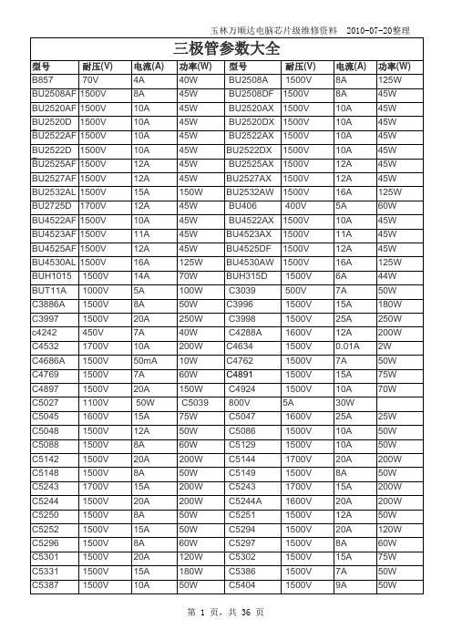
玉林万顺达电脑芯片级维修资料 2010-07-20整理玉林万顺达电脑芯片级维修资料 2010-07-20整理玉林万顺达电脑芯片级维修资料 2010-07-20整理玉林万顺达电脑芯片级维修资料 2010-07-20整理玉林万顺达电脑芯片级维修资料 2010-07-20整理玉林万顺达电脑芯片级维修资料 2010-07-20整理玉林万顺达电脑芯片级维修资料 2010-07-20整理玉林万顺达电脑芯片级维修资料 2010-07-20整理玉林万顺达电脑芯片级维修资料 2010-07-20整理玉林万顺达电脑芯片级维修资料 2010-07-20整理玉林万顺达电脑芯片级维修资料 2010-07-20整理玉林万顺达电脑芯片级维修资料 2010-07-20整理玉林万顺达电脑芯片级维修资料 2010-07-20整理玉林万顺达电脑芯片级维修资料 2010-07-20整理玉林万顺达电脑芯片级维修资料 2010-07-20整理玉林万顺达电脑芯片级维修资料 2010-07-20整理玉林万顺达电脑芯片级维修资料 2010-07-20整理玉林万顺达电脑芯片级维修资料 2010-07-20整理玉林万顺达电脑芯片级维修资料 2010-07-20整理玉林万顺达电脑芯片级维修资料 2010-07-20整理玉林万顺达电脑芯片级维修资料 2010-07-20整理玉林万顺达电脑芯片级维修资料 2010-07-20整理玉林万顺达电脑芯片级维修资料 2010-07-20整理玉林万顺达电脑芯片级维修资料 2010-07-20整理玉林万顺达电脑芯片级维修资料 2010-07-20整理玉林万顺达电脑芯片级维修资料 2010-07-20整理玉林万顺达电脑芯片级维修资料 2010-07-20整理玉林万顺达电脑芯片级维修资料 2010-07-20整理玉林万顺达电脑芯片级维修资料 2010-07-20整理玉林万顺达电脑芯片级维修资料 2010-07-20整理。

191001121910011262AC 1900RE580DCOPYRIGHT & TRADEMARKSSpecifications are subject to change without notice. is a registered trademark of TP-LINK TECHNOLOGIES CO., LTD. Other brands and product names are trademarks or registered trademarks of their respective holders.No part of the specifications may be reproduced in any form or by any means or used to make any derivative such as translation, transformation, or adaptation without permission from TP-LINK TECHNOLOGIES CO., LTD. Copyright ©2015 TP-LINK TECHNOLOGIES CO., LTD.All rights reserved.FCC STATEMENTThis equipment has been tested and found to comply with the limits for a Class B digital device, pursuant to part 15 of the FCC Rules. These limits are designed to provide reasonable protection against harmful interference in a residential installation. This equipment generates, uses and can radiate radio frequency energy and, if not installed and used in accordance with the instructions, may cause harmful interference to radio communications. However, there is no guarantee that interference will not occur in a particular installation. If this equipment does cause harmful interference to radio or television reception, which can be determined by turning the equipment off and on, the user is encouraged to try to correct the interference by one or more of the following measures:●Reorient or relocate the receiving antenna.●Increase the separation between the equipment and receiver.●Connect the equipment into an outlet on a circuit different from that towhich the receiver is connected.●Consult the dealer or an experienced radio/ TV technician for help. This device complies with part 15 of the FCC Rules. Operation is subject to the following two conditions:1)This device may not cause harmful interference.2)This device must accept any interference received, includinginterference that may cause undesired operation.Any changes or modifications not expressly approved by the party responsible for compliance could void the user’s authority to operate the equipment.Note: The manufacturer is not responsible for any radio or tv interference caused by unauthorized modifications to this equipment. Such modifications could void the user’s authority to operate the equipment.FCC RF Radiation Exposure StatementThis equipment complies with FCC RF radiation exposure limits set forth for an uncontrolled environment. This device and its antenna must not be co-located or operating in conjunction with any other antenna or transmitter. “To comply with FCC RF exposure compliance requirements, this grant is applicable to only Mobile Configurations. The antennas used for this transmitter must be installed to provide a separation distance of at least 20 cm from all persons and must not be co-located or operating in conjunction with any other antenna or transmitter.”CE Mark WarningThis is a class B product. In a domestic environment, this product may cause radio interference, in which case the user may be required to take adequate measures.National RestrictionsThis device is intended for home and office use in all EU countries (and other countries following the EU directive 1999/5/EC) without any limitationCountry Restriction Reason/remarkBulgaria None General authorization required foroutdoor use and public serviceFrance Outdoor use limited to10 mW e.i.r.p. withinthe band 2454-2483.5MHz Military Radiolocation use. Refarming of the 2.4 GHz band has been ongoing in recent years to allow current relaxed regulation. Full implementation planned 2012Italy None If used outside of own premises,general authorization is required Luxembourg None General authorization required fornetwork and service supply(not forspectrum)Norway Implemented This subsection does not apply forthe geographical area within a radiusof 20 km from the centre of Ny-ÅlesundRussian Federation None Only for indoor applications Note: Please don’t use the product outdoors in France.5150-5250 MHzCountry Restriction Reason/remarkBulgaria Not implemented PlannedCroatia License requiredItaly General authorization required if used outside own premisesLuxembourg None General authorization required fornetwork and service supply (not forspectrum)Russian Federation No infoNote: Operations in the 5.15-5.25GHz band are restricted to indoor usage only.Canadian Compliance StatementThis device complies with Industry Canada license-exempt RSSs. Operation is subject to the following two conditions:1)This device may not cause interference, and2)This device must accept any interference, including interference thatmay cause undesired operation of the device.Le présent appareil est conforme aux CNR d'Industrie Canada applicables aux appareils radio exempts de licence. L'exploitation est autorisée aux deux conditions suivantes :1)l'appareil nedoit pas produire de brouillage, et2)l'utilisateur de l'appareil doit accepter tout brouillage radioélectriquesubi, même si le brouillage est susceptible d'en compromettre le fonctionnement.Industry Canada StatementComplies with the Canadian ICES-003 Class B specifications.Cet appareil numérique de la classe B est conforme à la norme NMB-003 du Canada.CAN ICES-3 (B)/NMB-3(B)Radiation Exposure Statement:This equipment complies with IC radiation exposure limits set forth for an uncontrolled environment. This equipment should be installed and operated with minimum distance 20cm between the radiator & your body.Déclaration d'exposition aux radiations:Cet équipement est conforme aux limites d'exposition aux rayonnements IC établies pour un environnement non contrôlé. Cet équipement doit être installé et utilisé avec un minimum de 20 cm de distance entre la source de rayonnement et votre corps.Korea Warning Statements당해무선설비는운용중전파혼신가능성이있음.NCC Notice & BSMI Notice注意!依據低功率電波輻射性電機管理辦法第十二條經型式認證合格之低功率射頻電機,非經許可,公司、商號或使用者均不得擅自變更頻率、加大功率或變更原設計之特性或功能。

Measurement conditionAmbient temperature: 25 °CInput power level: 0 dBmTerminating impedance: *Input: 330 Ω || -13,5 pFOutput: 380 Ω || -15,2 pFCharacteristicsRemark:The reference level for the relative attenuation a rel of the TFS 153E is the minimum of the pass band attenuation a min. The minimum of the pass band attenuation a min is defined as the insertion loss a e. The centre frequency f c is the arithmetic mean value of the upper and lower frequencies at the 3 dB filter attenuation level relative to the insertion loss a e. The temperature coefficient of frequency Tc f is valid for both the reference frequency f c and the frequency response of the filter in the operating temperature range. The frequency shift of the filter in the operating temperature range is not included in the production tolerance scheme.D a t a typ. value tolerance / limit Insertion loss a e21,1 dB max. 25 dB (reference level)Nominal frequency f N - 153,5 MHzCentre frequency f C 153,5 MHz ± 0,1 MHzPassband PB - f C ±2,5015 MHzPass band ripple (p-p) 0,3 dB max. 0,7 dBBandwidth BW0,7 dB 5,30 dB min. 5,03 MHz3 dB 5,65 dB min. 5,60 MHz 15 dB 6,21 dB max. 6,30 MHz 45 dB 6,68 dB max. 9,70 MHz Relative attenuation a relf C …f C ± 2,5015 MHz 0,3 dB max. 0,7 dBf C ± 2,5015 MHz …f C ± 2,800 MHz 2,5 dB max. 3,0 dBf C - 144,500 MHz …f C - 4,825 MHz 60 dB min. 45 dBf C ± 3,150 MHz …f C ± 3,350 MHz 17 dB min. 15 dBf C ± 3,350 MHz …f C ± 3,750 MHz 30 dB min. 25 dBf C ± 3,750 MHz …f C ± 4,825 MHz 55 dB min. 40 dBf C + 4,825 MHz …f C + 428,500 MHz 55 dB min. 45 dB Absolute group delay within PB 2,5 µs max. 2,7 µsGroup delay ripple within PB (p-p) 60 max. 120 nsOperating temperature range OTR - - 25 °C ... + 80°CStorage temperature range - - 40 °C ... + 85°C Frequency inversion temperature 20 °C - Temperature coefficient of frequency TC f ** -0,036 ppm/K2 -*) The terminating impedances depend on parasitics and q-values of matching elements and the board used, and are to be understood as reference values only. Should there be additional questions do not hesitate to ask for an application note or contact our design team.**) f c(Hz) = Tc f(ppm/K2) x (T - T A)2 x f CAT (MHz)Generated:Checked / Approved:Microchip Frequency Technology GmbHPotsdamer Straße 18D 14 513 TELTOW / GermanyMicrochip Frequency Technology GmbH Potsdamer Straße 18 D 14 513 TELTOW / GermanyConstruction and pin connection(All dimensions in mm)50 Ω Test circuit1 Input RF Return2 Ground3 Ground4 Ground5 Output6 Output RF Return7 Ground8 Ground9 Ground 10 InputDate code: Year + week V 2007 W 2008 X 2009 ...Microchip Frequency Technology GmbH Potsdamer Straße 18 D 14 513 TELTOW / Germany Stability characteristics, reliabilityAfter the following tests the filter shall meet the whole specification:1. Shock: 500g, 1 ms, half sine wave, 3 shocks each plane; DIN IEC 68 T2 - 272. Vibration: 10 Hz to 500 Hz, 0,35 mm or 5 g respectively, 1 octave per min, 10 cycles per plan, 3 plans; DIN IEC 68 T2 - 63. Change of temperature: -55 °C to 125°C / 30 min. each / 10 cycles DIN IEC 68 part 2 – 14 Test N4. Resistance tosolder heat (reflow): reflow possible: three times max.; for temperature conditions refer to the attached "Air reflow temperature conditions" on page 4;5. ESD ANSI/ESD S20.20-1999, class 1A for HBMThis filter is RoHS compliant (2002/95/EG, 2005/618/EG)PackingTape & Reel: IEC 286 – 3, with exception of value for N and minimum bending radius; tape type II, embossed carrier tape with top cover tape on the upper side; max. pieces of filters per reel:<MAXPIECESPERREEL>reel of empty components at start:min. 300 mm reel of empty components at start including leader: min. 500 mm trailer: min. 300 mmS oWDo P oEC tP 2P 1D1B oAoP ull Off DirectionT ype P IN MarkerDate CodetK oThe minimum bending radius is 45 mm.Air reflow temperature conditionsTape (all dimensions in mm) W : 44,00 ± 0,3 Po : 4,00 ± 0,1 Do : 1,50 +0,1/-0 E : 1,75 ± 0,1 F : 20,20 ± 0,15 P2 : 2,00 ± 0,15 P1 : 16,00 ± 0,1 D1(min) : 2,00 Ao : 9,30 ± 0,1 Bo : 24,90 ± 0,1 So : 40,40 ± 0,1 Ct : 38,0 ± 0,1 Reel (all dimensions in mm) A : 330 W1 : 44,4 +2/-0 W2(max) : 50,4 N(min) : 100 C : 13,0 +0,5/-0,2Microchip Frequency Technology GmbH Potsdamer Straße 18D 14 513 TELTOW / GermanyHistoryVersion Reason of changes Name Date1.0 - development specification Pfeiffer 03.01.2007 1.1 - add of terminating impedances and typical values Pfeiffer 18.01.2007- filter characteristics correctedMicrochip Frequency Technology GmbHPotsdamer Straße 18D 14 513 TELTOW / Germany。

定时器的解释TCON:定时器控制寄存器寄存器地址88H,位寻址8FH~88H。
位地址 8F 8E 8D 8C 8B 8A 89 88位符号 TF1 TR1 TF0 TR0 IE1 IT1 IE0 IT0TF0(TF1)——计数溢出标志位,当计数器计数溢出时,该位置1。
TR0(TR1)——定时器运行控制位当TR0(TR1)=0 停止定时器/计数器工作当TR0(TR1)=1 启动定时器/计数器工作IE0(IE1)——外中断请求标志位当CPU采样到P3.2(P3.3)出现有效中断请求时,此位由硬件置1。
在中断响应完成后转向中断服务时,再由硬件自动清0。
IT0(IT1)——外中断请求信号方式控制位当IT0(IT1)=1脉冲方式(后沿负跳有效)当IT0(IT1)=0电平方式(低电平有效)此位由软件置1或清0。
TF0(TF1)——计数溢出标志位当计数器产生计数溢出时,此位由硬件置1。
当转向中断服务时,再有硬件自动清0。
计数溢出的标志位的使用有两种情况:采用中断方式时,作中断请求标志位来使用;采用查询方式时,作查询状态位来使用。
TMOD寄存器定时器/计数器T0¦T1的方式寄存器GATE C/T M1 M0 GATE C/T M1 M0其中低四位定义定时器/计数器T0,高四位定义定时器/计数器T1,各位的说明:Ⅰ,GATE——门控制。
GATE=1时,由外部中断引脚INT0、INT1和控制寄存器的TR0,TR1来启动定时器。
GATE=0时,仅由TR0,TR1置位分别启动定时器T0、T1。
Ⅱ,C/T——功能选择位置位时选择计数功能,清零时选择定时功能。
Ⅲ,M0、M1——方式选择功能由于有2位,因此有4种工作方式================================================================ M1M0 工作方式计数器模式 TMOD(设置定时器模式)0 0 方式0 13位计数器 TMOD=0x000 1 方式1 16位计数器 TMOD=0x011 0 方式2 自动重装8位计数器 TMOD=0x021 1 方式3 T0分为2个8位计数器,T1为波特率发生器 TMOD=0x03================================================================中断向量号以及USING n的解释5、IE-----中断充许寄存器按位寻址,地址:A8HB7 B6 B5 B4 B3 B2 B1 B0EA ET2 ES ET1 EX1 ET0 EX0EA (IE.7):EA=0时,所有中断禁止(即不产生中断)EA=1时,各中断的产生由个别的允许位决定- (IE.6):保留ET2(IE.5):定时2溢出中断充许(8052用)ES (IE.4):串行口中断充许(ES=1充许,ES=0禁止)ET1(IE.3):定时1中断充许EX1(IE.2):外中断INT1中断充许ET0(IE.1):定时器0中断充许EX0(IE.0):外部中断INT0的中断允许本篇文章来源于百科网络转载请以链接形式注明出处网址:/dianqia/danpianji/200911/1042580_3.html1、返回值函数名 interrupt n其中n 对应中断源的编号,其值从0 开始,以80C51 单片机为例,编号从0~4,分别对应外中断0、定时器0 中断、外中断1、定时器1 中断和串行口中断。


51单片机定时器/计数器的结构和原理作者:佚名来源:不详录入:Admin更新时间:2008-7-26 19:47:15点击数:3【字体:】定时器、计数器定时器/计数器简称定时器,其作用主要包括产生各种时标间隔、记录外部事件的数量等,是微机中最常用、最基本的部件之一。
803l单片机有2个16位的定时器/计数器:定时器0(T0)和定时器1(T1)。
T0由2个定时寄存器TH0和TL0构成,T1则由TH1和TL1构成,它们都分别映射在特殊功能寄存器中,从而可以通过对特殊功能寄存器中这些寄存器的读写来实现对这两个定时器的操作。
作定时器时,每一个机器周期定时寄存器自动加l,所以定时器也可看作是计量机器周期的计数器。
由于每个机器周期为12个时钟振荡周期,所以定时的分辨率是时钟振荡频率的1/12。
作计数器时,只要在单片机外部引脚T0(或T1)有从1到0电平的负跳变,计数器就自动加1。
计数的最高频率一般为振荡频率的l/24。
工作方式:T0或T1无论用作定时器或计数器都有4种工作方式:方式0、方式1、方式2和方式3。
除方式3外,T0和T1有完全相同的工作状态。
下面以T1为例,分述各种工作方式的特点和用法。
1、工作方式0:13位方式由TL1的低5位和TH1的8位构成13位计数器(TL1的高3位无效)。
工作方式0的结构见下图:图中,C/T为定时/计数选择:C/T=0,T1为定时器,定时信号为振荡周期12分频后的脉冲;C/T =l,T1为计数器,计数信号来自引脚T1的外部信号。
定时器T1能否启动工作,还受到了R1、GATE和引脚信号INT1的控制。
由图中的逻辑电路可知,当GATE=0时,只要TR1=1就可打开控制门,使定时器工作;当GATE=1时,只有TR1=1且INT1=1,才可打开控制门。
GATE,TR1,C/T的状态选择由定时器的控制寄存器TMOD,TCON中相应位状态确定,INT1则是外部引脚上的信号。
在一般的应用中,通常使GATE=0,从而由TRl的状态控制Tl的开闭:TRl=1,打开T1;TRl=0,关闭T1。
TOSHIBA InGaAℓP LEDTLRE53T(F),TLRME53T(F),TLSE53T(F),TLOE53T(F),TLYE53T(F), TLPYE53T(F),TLGE53T(F),TLFGE53T(F),TLPGE53T(F)Panel Circuit Indicators•Lead(Pb)-free products (lead: Sn-Ag-Cu)•3mm package•InGaAℓP technology•All plastic mold•Transparent lens•Lineup: 6 colors (red, orange, yellow, pure yellow, green and pure green)•High intensity light emission•Excellent low current light output•Applications: message boards, security devices and dashboarddisplaysLineupUnit: mmJEDEC ―JEITA ―TOSHIBA 4-4E1A Weight: 0.14 g(Typ.)Product Name Color Material TLRE53T(F) RedTLRME53T(F) RedTLSE53T(F) RedTLOE53T(F) OrangeTLYE53T(F) Yellow TLPYE53T(F) PureYellow TLGE53T(F) Green TLFGE53T(F) Green TLPGE53T(F) PureGreenP InGaA lAbsolute Maximum Ratings (Ta = 25°C)Product Name Forward CurrentI F (mA)Reverse VoltageV R (V)Power DissipationP D (mW)OperatingTemperatureT opr (°C)StorageTemperatureT stg (°C)TLRE53T(F) 50 4 120TLRME53T(F) 50 4 120TLSE53T(F) 50 4 120TLOE53T(F) 50 4 120TLYE53T(F) 50 4 120TLPYE53T(F) 50 4 120TLGE53T(F) 50 4 120TLFGE53T(F) 50 4 120TLPGE53T(F) 50 4 120−40~100 −40~120Note: Using continuously under heavy loads (e.g. the application of high temperature/current/voltage and the significant change in temperature, etc.) may cause this product to decrease in the reliability significantly even if the operating conditions (i.e. operating temperature/current/voltage, etc.) are within the absolute maximum ratings.Please design the appropriate reliability upon reviewing the Toshiba Semiconductor Reliability Handbook(“Handling Precautions”/“Derating Concept and Methods”) and individual reliability data (i.e. reliability testreport and estimated failure rate, etc).Electrical and Optical Characteristics (Ta = 25°C)Typ. Emission Wavelength Luminous IntensityI VForward VoltageV FReverse CurrentI RProduct NameλdλPΔλI F Min Typ.I F Typ.Max I F Max V R TLRE53T(F) 630 (644) 20 20 153 400 20 1.9 2.4 20 50 4TLRME53T(F) 626 (636) 23 20 272 600 20 1.9 2.4 20 50 4TLSE53T(F) 613 (623) 20 20 272 800 20 1.9 2.4 20 50 4TLOE53T(F) 605 (612) 20 20 272 100020 2.0 2.4 20 50 4TLYE53T(F) 587 (590) 17 20 272 800 20 2.0 2.4 20 50 4TLPYE53T(F) 580 (583) 14 20 153 450 20 2.0 2.4 20 50 4TLGE53T(F) 571 (574) 17 20 153 400 20 2.0 2.4 20 50 4TLFGE53T(F) 565 (568) 15 20 85 200 20 2.0 2.4 20 50 4TLPGE53T (F) 558 (562) 14 20 47.6130 20 2.1 2.4 20 50 4 Unit nmmAmcdmAVmAμA V PrecautionsPlease be careful of the following:•Soldering temperature: 260°C max, soldering time: 3 s max(soldering portion of lead: up to 1.6 mm from the body of the device)•If the lead is formed, the lead should be formed up to 1.6 mm from the body of the device without forming stress to the resin. Soldering should be performed after lead forming.•This visible LED lamp also emits some IR light.If a photodetector is located near the LED lamp, please ensure that it will not be affected by this IR light.R e l at i v e l u m i n o u si n t e n s i t yForward voltage V F (V) I F – V FF o r w a r d cu r r e n t I F (m A )Forward current I F (mA)I V – I FL u m i no u s i n t e n si t y I V (m c d )Case temperature Tc (°C) I V – TcR e l a t i v e l u mi n o u s in t e n s i t y I VWavelength λ (nm)Relative luminous intensity – WavelengthAmbient temperature Ta (°C)I F – TaA l l o w a b l e fo r w a r d c u r r e n t I F (m A )Radiation patternTa = 25°C30°0°60° 90° 90°30° 60° 1.00.80.6 0.4 0.2 0 80° 70° 50° 40°20°10°70° 80° 50° 40° 20° 10°20 −20 800.1310.30.5 0 4060 060040802012020406080 100R e l at i v e l u m i n o u si n t e n s i t yForward voltage V F (V) I F – V FF o r w a r d c ur r e n t I F (m A )Forward current I F (mA)I V – I FL u m i n ou s i n t e ns i t y I V (m c d )Case temperature Tc (°C) I V – TcR e l a t i v e l u mi n o u s in t e n s i t y I VWavelength λ (nm)Relative luminous intensity – WavelengthAmbient temperature Ta (°C)I F – TaA l l o w a b l e fo r w a r d c u r r e n t I F (m A )Radiation patternTa = 25°C30°0°60° 90° 90°30° 60° 1.00.80.6 0.4 0.2 0 80° 70° 50° 40°20°10°70° 80° 50° 40° 20° 10°60040802012020406080100 20 −20 800.1310.30.5 0 4060 510R e l at i v e l u m i n o u si n t e n s i t yForward voltage V F (V) I F – V FF o r w a r d cu r r e n t I F (m A )Forward current I F (mA)I V – I FL u m i no u s i n t e n si t y I V (m c d )Case temperature Tc (°C) I V – TcR e l a t i v e l u mi n o u s in t e n s i t y I VWavelength λ (nm)Relative luminous intensity – WavelengthAmbient temperature Ta (°C)I F – TaA l l o w a b l e fo r w a r d c u r r e n t I F (m A )Radiation patternTa = 25°C30°0°60° 90° 90°30° 60° 1.00.80.6 0.4 0.2 0 80° 70° 50° 40°20°10°70° 80° 50° 40° 20°10°60040802012020406080 100 20 −20 800.1310.30.5 0 4060R e l at i v e l u m i n o u si n t e n s i t yForward voltage V F (V) I F – V FF o r w a r d c ur r e n t I F (m A )Forward current I F (mA)I V – I FL u m i no u s i n t e n si t y I V (m c d )Case temperature Tc (°C) I V – TcR e l a t i v e l u mi n o u s in t e n s i t y I VWavelength λ (nm)Relative luminous intensity – WavelengthAmbient temperature Ta (°C)I F – TaA l l o w a b l e fo r w a r d c u r r e n t I F (m A )Radiation patternTa = 25°C30°0°60° 90° 90°30° 60° 1.00.80.6 0.4 0.2 0 80° 70° 50° 40°20°10°70° 80° 50° 40° 20° 10°60040802012020406080 10020 −20 800.1310.30.5 0 4060R e l at i v e l u m i n o u si n t e n s i t yForward voltage V F (V) I F – V FF o r w a r d c ur r e n t I F (m A )Forward current I F (mA)I V – I FL u m i no u s i n t e n si t y I V (m c d )Case temperature Tc (°C) I V – TcR e l a t i v e l u mi n o u s in t e n s i t y I VWavelength λ (nm)Relative luminous intensity – WavelengthAmbient temperature Ta (°C)I F – TaA l l o w a b l e fo r w a r d c u r r e n t I F (m A )Radiation patternTa = 25°C30°0°60° 90° 90°30° 60° 1.00.80.6 0.4 0.2 0 80° 70° 50° 40°20°10°70° 80° 50° 40° 20° 10°60040802012020406080 10020 −20 800.1310.30.5 0 4060100R e l a t i v e l u m i n o u s i n t e n s i t yForward voltage V F (V)I F – V FF o r w a r d c u r r e n t I F (m A )Forward current I F (mA)I V– I FL u m in o u s i n t e n s i t y I V (m c d )Case temperature Tc (°C)I V – TcR e l a t iv e l u m i n o u s i n t e n s i t y I VWavelength λ (nm)Relative luminous intensity – WavelengthAmbient temperature Ta (°C)I F – TaA l l o w a b l e f o r w a r d c u r r e n t I F (m A )Radiation patternTa = 25°C30°0°60° 90° 90°30° 60° 1.00.80.6 0.4 0.2 0 80° 70° 50° 40°20°10°70° 80° 50° 40° 20° 10°60040802012020406080 100 20 −20 805 0.131010.30.50 40 60 100R e l at i v e l u m i n o u si n t e n s i t yForward voltage V F (V) I F – V FF o r w a r d c ur r e n t I F (m A )Forward current I F (mA)I V – I FL u m i no u s i n t e n si t y I V (m c d )Case temperature Tc (°C) I V – TcR e l a t i v e l u mi n o u s in t e n s i t y I VWavelength λ (nm)Relative luminous intensity – WavelengthAmbient temperature Ta (°C)I F – TaA l l o w a b l e fo r w a r d c u r r e n t I F (m A )Radiation patternTa = 25°C30°0°60° 90° 90°30° 60° 1.00.80.6 0.4 0.2 0 80° 70° 50° 40°20°10°70° 80° 50° 40° 20° 10°60040802012020406080100 20 −20 800.1310.30.5 0 4060 5 10100R e l a t i v e l u m i n o u s i n t e n s i t yForward voltage V F (V) IF – V FFo r w a r d c u r r e n t I F (m A )Forward current I F (mA)I V – I FL u m i no u s i n t e n s i t y I V (m c d )Case temperature Tc (°C) I V – TcR e l a t i ve l u m i n o u s i n t e n s i t y I VWavelength λ (nm)Relative luminous intensity – WavelengthAmbient temperature Ta (°C)I F – TaA l l o w a b l e f o r w a r d c u r r e n t I F (m A )Radiation patternTa = 25°C30°0°60° 90° 90°30° 60° 1.00.80.6 0.4 0.2 0 80° 70° 50° 40°20°10°70° 80° 50° 40° 20° 10°60040802012020406080 100 560520640540580 600 620 20 −20805 0.131010.30.5 0 40 60 100TLPGE53T(F)R e l a t i v e l u m i n o u si n t e n s i t yForward voltage V F (V) I F – V FF o r w a r d cu r r e n t I F (m A )Forward current I F (mA)I V – I FL u m i n ou s i n t e ns i t y I V (m c d )Case temperature Tc (°C) I V – TcR e l a t i v e l u mi n o u s i n te n s i t y I VWavelength λ (nm)Relative luminous intensity – WavelengthAmbient temperature Ta (°C)I F – TaA l l o w a b l e f or w a r d c u r r e n t I F (m A )Radiation patternTa =25°C30°0°60° 90° 90°30° 60° 1.00.80.6 0.4 0.2 0 80° 70° 50° 40°20°10°70° 80° 50° 40° 20°10°60040802012020406080100 20 −20 800.1310.30.5 0 4060 5 10RESTRICTIONS ON PRODUCT USE20070701-EN •The information contained herein is subject to change without notice.•TOSHIBA is continually working to improve the quality and reliability of its products. Nevertheless, semiconductor devices in general can malfunction or fail due to their inherent electrical sensitivity and vulnerability to physical stress. It is the responsibility of the buyer, when utilizing TOSHIBA products, to comply with the standards of safety in making a safe design for the entire system, and to avoid situations in which a malfunction or failure of such TOSHIBA products could cause loss of human life, bodily injury or damage to property.In developing your designs, please ensure that TOSHIBA products are used within specified operating ranges as set forth in the most recent TOSHIBA products specifications. Also, please keep in mind the precautions and conditions set forth in the “Handling Guide for Semiconductor Devices,” or “TOSHIBA Semiconductor Reliability Handbook” etc.• The TOSHIBA products listed in this document are intended for usage in general electronics applications (computer, personal equipment, office equipment, measuring equipment, industrial robotics, domestic appliances, etc.).These TOSHIBA products are neither intended nor warranted for usage in equipment that requires extraordinarily high quality and/or reliability or a malfunction or failure of which may cause loss of human life or bodily injury (“Unintended Usage”). Unintended Usage include atomic energy control instruments, airplane or spaceship instruments, transportation instruments, traffic signal instruments, combustion control instruments, medical instruments, all types of safety devices, etc.. Unintended Usage of TOSHIBA products listed in his document shall be made at the customer’s own risk.•The products described in this document shall not be used or embedded to any downstream products of which manufacture, use and/or sale are prohibited under any applicable laws and regulations.• The information contained herein is presented only as a guide for the applications of our products. No responsibility is assumed by TOSHIBA for any infringements of patents or other rights of the third parties which may result from its use. No license is granted by implication or otherwise under any patents or other rights of TOSHIBA or the third parties.•GaAs(Gallium Arsenide) is used in this product. The dust or vapor is harmful to the human body. Do not break, cut, crush or dissolve chemically.• Please contact your sales representative for product-by-product details in this document regarding RoHS compatibility. Please use these products in this document in compliance with all applicable laws and regulations that regulate the inclusion or use of controlled substances. Toshiba assumes no liability for damage or losses occurring as a result of noncompliance with applicable laws and regulations.。