SM1145C中文资料
- 格式:pdf
- 大小:77.83 KB
- 文档页数:2


SOCAY瞬变二极管SMAJ54C型号
硕凯电子(Sylvia)
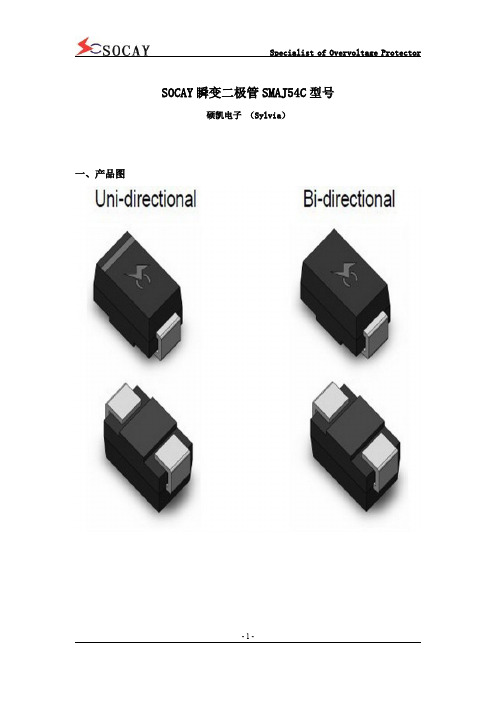
一、产品图
1、为表面安装应用优化电路板空间
2、低泄漏
3、单向单元
4、玻璃钝化结
5、低电感
6、优良的钳位能力
7、400W的峰值功率能力在10×1000μ波形重复率(占空比):0.01%
8、快速响应时间:从0伏特到最小击穿电压通常小于1.0ps
9、典型的,在电压高于12V时,反向漏电流小于5μA
10、高温焊接:终端260°C/40秒
11、典型的最大温度系数△Vbr=0.1%x Vbr@25°C x△T
12、塑料包装有保险商实验室可燃性94V-0
13、无铅镀雾锡
14、无卤化,符合RoHS
15、典型失效模式是在指定的电压或电流下出现
16、晶须测试是基于JEDEC JESD201A每个表4a及4c进行的
17、IEC-61000-4-2ESD15kV(空气),8kV(接触)
18、数据线的ESD保护符合IEC61000-4-2(IEC801-2)
19、数据线的EFT保护符合IEC61000-4-4(IEC801-4)
三、应用范围
TVS器件非常适合保护I/O接口,Vcc总线和其他应用于电信、计算机、工业和消费电子应用的易损电路。
五、UL认证编号
六、特性曲线
七、产品尺寸。

1.General descriptionThe TJA1145 is a high-speed CAN transceiver that provides an interface between aController Area Network (CAN) protocol controller and the physical two-wire CAN bus.The transceiver is designed for high-speed CAN applications in the automotive industry,providing differential transmit and receive capability to (a microcontroller with) a CANprotocol controller.The TJA1145 features very low power consumption in Standby and Sleep modes andsupports ISO 11898-2:2016 compliant CAN Partial Networking by means of a selectivewake-up function.A dedicated implementation of the partial networking function has been embedded intothe TJA1145/FD variants TJA1145T/FD and TJA1145TK/FD (see Section7.3.2 for furtherdetails on CAN FD). This function is called ‘FD-passive’ and is the ability to ignore CANFD frames while waiting for a valid wake-up frame in Sleep/Standby mode. This additionalfeature of partial networking is the perfect fit for networks that support both CAN FD andstandard CAN 2.0 communications. It allows normal CAN controllers that do not need tocommunicate CAN FD messages to remain in partial networking Sleep/Standby modeduring CAN FD communication without generating bus errors.Advanced power management regulates the supply throughout the node and supportslocal and remote wake-up functionality. I/O levels are automatically adjusted to the I/Olevels of the controller, allowing the TJA1145 to interface directly with 3.3 V to 5 Vmicrocontrollers. An SPI interface is provided for transceiver control and for retrievingstatus information. Bus connections are truly floating when power is off.The TJA1145 implements the CAN physical layer as defined in ISO 11898-2:2016 andSAE J2284-1 to SAE J2284-4. This implementation enables reliable communication in theCAN FD fast phase at data rates up to 2 Mbit/s.These features make the TJA1145 the ideal choice for high-speed CAN networkscontaining nodes that are always connected to the battery supply line but, in order tominimize current consumption, are only active when required by the application.2.Features and benefits2.1General⏹ISO 11898-2:2016 and SAE J2284-1 to SAE J2284-4 compliant⏹Timing guaranteed for data rates up to 2Mbit/s⏹Autonomous bus biasing according to ISO 11898-2:2016⏹Optimized for in-vehicle high-speed CAN communication⏹No ‘false’ wake-ups due to CAN FD in TJA1145/FD variantsNXP Semiconductors TJA1145High-speed CAN transceiver for partial networking2.2Designed for automotive applications⏹±8 kV ElectroStatic Discharge (ESD) protection, according to the Human Body Model(HBM) on the CAN bus pins⏹±6 kV ESD protection, according to IEC 61000-4-2 on pins BAT and WAKE and on theCAN bus pins⏹CAN bus pins short-circuit proof to ±58 V⏹Battery and CAN bus pins protected against transients according to ISO7637-3, testpulses 1, 2a, 3a and 3b.⏹Suitable for use in 12 V and 24 V systems⏹Available in SO14 and leadless HVSON14 package (3 mm ⨯ 4.5 mm) with improvedAutomated Optical Inspection (AOI) capability⏹AEC-Q100 qualified⏹Dark green product (halogen free and Restriction of Hazardous Substances (RoHS)compliant)3.Quick reference dataTable 1.Quick reference dataSymbol Parameter Conditions Min Typ Max Unit V BAT battery supply voltage 4.5-28VV CC supply voltage 4.5- 5.5VV IO supply voltage on pin V IO 2.85- 5.5VV BAT falling 2.8-3V V th(det)poff power-off detection thresholdvoltage4.5- 4.75V V uvd(VCC)undervoltage detection voltageon pin VCCV uvd(VIO)undervoltage detection voltageV BAT >4.5V 2.7- 2.85V on pin VIOI BAT battery supply current Normal mode-1 1.5mA-4059μASleep mode; CAN Offline mode;-40︒C < T vj<85︒C; V BAT = 7V to 18V-4468μAStandby mode; CAN Offline mode;-40︒C < T vj<85︒C; V BAT = 7V to 18VI CC supply current CAN Active mode; CAN recessive; V TXD=V IO-36mACAN Active mode; CAN dominant; V TXD=0V-4565mA- 4.78.5μAStandby/Normal mode; CAN inactive;-40︒C < T vj<85︒CSleep mode; CAN inactive; -40︒C < T vj<85︒C- 3.87μA I IO supply current on pin V IO Standby/Normal mode; -40︒C < T vj<85︒C-7.111μASleep mode; -40︒C < T vj<85︒C-58μA V ESD electrostatic discharge voltage IEC 61000-4-2 on pins CANH, CANL-6-+6kV V CANH voltage on pin CANH-58-+58VV CANL voltage on pin CANL-58-+58VT vj virtual junction temperature-40-+150︒C4.Ordering information5.Block diagramTable 2.Ordering informationType numberPackage NameDescriptionVersion TJA1145T SO14plastic small outline package; 14leads; body width 3.9mm SOT108-1TJA1145T/FD SO14plastic small outline package; 14leads; body width 3.9mm SOT108-1TJA1145TK HVSON14plastic thermal enhanced very thin small outline package; no leads;14terminals; body 3 ⨯ 4.5 ⨯ 0.85 mmSOT1086-2TJA1145TK/FDHVSON14plastic thermal enhanced very thin small outline package; no leads; 14terminals; body 3 ⨯ 4.5 ⨯ 0.85 mmSOT1086-26.Pinning information6.1Pinning6.2Pin descriptionTable 3.Pin descriptionSymbol Pin DescriptionTXD1transmit data inputGND2[1]groundVCC3 5 V CAN transceiver supply voltageRXD4receive data output; reads out data from the bus linesVIO5supply voltage for I/O level adaptorSDO6SPI data outputINH7inhibit output for switching external voltage regulatorsSCK8SPI clock inputWAKE9local wake-up inputBAT10battery supply voltageSDI11SPI data inputCANL12LOW-level CAN bus lineCANH13HIGH-level CAN bus lineSCSN14SPI chip select input[1]HVSON14 package die supply ground is connected to both the GND pin and the exposed center pad. TheGND pin must be soldered to board ground. For enhanced thermal and electrical performance, it isrecommended that the exposed center pad also be soldered to board ground。

SMF05C, SMF12C, SMF15C,SMF24C5−Line Transient Voltage Suppressor ArrayThis 5−line voltage transient suppressor array is designed for application requiring transient voltage protection capability. It is intended for use in over−transient voltage and ESD sensitive equipment such as computers, printers, automotive electronics,networking communication and other applications. This device features a monolithic common anode design which protects five independent lines in a single SC−88 package.Features•Protects up to 5−Line in a Single SC−88 Package•Peak Power Dissipation − 100 W (8 x 20 m s Waveform)•ESD Rating of Class 3B (Exceeding 8 kV) per Human Body Model and Class C (Exceeding 400 V) per Machine Model.•Compliance with IEC 61000−4−2 (ESD) 15 kV (Air), 8 kV (Contact)•Flammability Rating of UL 94 V−0•Pb−Free Package is Available Applications•Hand−Held Portable Applications •Networking and Telecom •Automotive Electronics •Serial and Parallel Ports•Notebooks, Desktops, ServersMAXIMUM RATINGS (T J =25°C unless otherwise specified)Maximum ratings are those values beyond which device damage can occur.Maximum ratings applied to the device are individual stress limit values (not normal operating conditions) and are not valid simultaneously. If these limits are exceeded, device functional operation is not implied, damage may occur and reliability may be affected.1.Nonrepetitive current pulse per Figure 3.DevicePackage Shipping †ORDERING INFORMATIONSMF05CT1SC−883000/T ape & Reel SMF12CT1SC−883000/T ape & Reel SMF15CT1SC−883000/T ape & Reel SMF24CT1SC−883000/T ape & Reel†For information on tape and reel specifications,including part orientation and tape sizes, please refer to our Tape and Reel Packaging Specification Brochure, BRD8011/D.*The “T2” suffix refers to an alternate tape & reel orientation.SMF05CT2*SC−883000/T ape & Reel SMF05CT2G*SC−88(Pb−Free)3000/T ape & ReelSMF05C ELECTRICAL CHARACTERISTICS (T J = 25°C unless otherwise specified)SMF12C ELECTRICAL CHARACTERISTICS (T J = 25°C unless otherwise specified)SMF15C ELECTRICAL CHARACTERISTICS (T = 25°C, unless otherwise specified)SMF24C ELECTRICAL CHARACTERISTICS (T = 25°C, unless otherwise specified)S devices are normally selected according to the working peak reverse voltage (V RWM), which should be equal or greater than the DCor continuous peak operating voltage level.3.V BR is measured at pulse test current I T.TYPICAL PERFORMANCE CURVES(T J = 25°C unless otherwise specified)Figure 1. Pulse Derating Curve10090807060504030201000255075100125175200T A , AMBIENT TEMPERATURE (°C)Figure 2. 8 × 20 m s Pulse Waveform1009080706050403020100t, TIME (m s)% O F P E A K P U L S E C U R R E N TFigure 3. Clamping Voltage vs Peak Pulse Current 100101I PP , PEAK PULSE CURRENT (A)V C L A M P , C L A M P I N G V O L T A G E (V )Figure 4. Junction Capacitance vs Reverse VoltageV BR , REVERSE VOLTAGE (V)P E A K P O W E R D I S S I P A T I O N (%)PACKAGE DIMENSIONSSTYLE 24:PIN 1.CATHODE2.ANODE3.CATHODE4.CATHODE5.CATHODE6.CATHODENOTES:1.DIMENSIONING AND TOLERANCING PER ANSI Y14.5M, 1982.2.CONTROLLING DIMENSION: INCH.3.419B−01 OBSOLETE, NEW STANDARD 419B−02.DIM A MIN MAX MIN MAX MILLIMETERS 1.80 2.200.0710.087INCHES B 1.15 1.350.0450.053C 0.80 1.100.0310.043D 0.100.300.0040.012G 0.65 BSC 0.026 BSC H −−−0.10−−−0.004J 0.100.250.0040.010K 0.100.300.0040.012N 0.20 REF 0.008 REF S2.00 2.200.0790.087SC−88/SC70−6/SOT−363CASE 419B−02ISSUE 02U*For additional information on our Pb−Free strategy and solderingdetails, please download the ON Semiconductor Soldering and Mounting Techniques Reference Manual, SOLDERRM/D.SOLDERING FOOTPRINT*ON Semiconductor and are registered trademarks of Semiconductor Components Industries, LLC (SCILLC). SCILLC reserves the right to make changes without further notice to any products herein. SCILLC makes no warranty, representation or guarantee regarding the suitability of its products for any particular purpose, nor does SCILLC assume any liability arising out of the application or use of any product or circuit, and specifically disclaims any and all liability, including without limitation special, consequential or incidental damages.“Typical” parameters which may be provided in SCILLC data sheets and/or specifications can and do vary in different applications and actual performance may vary over time. All operating parameters, including “Typicals” must be validated for each customer application by customer’s technical experts. SCILLC does not convey any license under its patent rights nor the rights of others. SCILLC products are not designed, intended, or authorized for use as components in systems intended for surgical implant into the body, or other applications intended to support or sustain life, or for any other application in which the failure of the SCILLC product could create a situation where personal injury or death may occur. Should Buyer purchase or use SCILLC products for any such unintended or unauthorized application, Buyer shall indemnify and hold SCILLC and its officers, employees, subsidiaries, affiliates,and distributors harmless against all claims, costs, damages, and expenses, and reasonable attorney fees arising out of, directly or indirectly, any claim of personal injury or death associated with such unintended or unauthorized use, even if such claim alleges that SCILLC was negligent regarding the design or manufacture of the part. SCILLC is an Equal Opportunity/Affirmative Action Employer. This literature is subject to all applicable copyright laws and is not for resale in any manner.PUBLICATION ORDERING INFORMATION。

Rev. 0 Document Feedback Information furnished by Analog Devices is believed to be accurate and reliable.However,no responsibility is assumed by Analog Devices for its use, nor for any infringements of patents or other rights of third parties that may result from its use. Specifications subject to change without notice. No license is granted by implication or otherwise under any patent or patent rights of Analog Devices. Trademarks and registered trademarks are the property of their respective owners. One Technology Way, P.O. Box 9106, Norwood, M A 02062-9106, U.S.A. Tel: 781.329.4700 ©2019 Analog Devices, Inc. All rights reserved. Technical Support /cn16位隔离式∑-∆调制器数据手册ADuM7701产品特性主机时钟输入频率:5 MHz至21 MHz失调漂移与温度的关系:±0.6 μV/°C(最大值)SNR:86 dB(典型值)16位无失码满量程模拟输入电压范围:±320 mVENOB:14位(典型值)I DD1:10 mA(最大值)板载数字隔离器工作温度范围:−40°C至+125°C高共模瞬变抗扰度:150 kV/μs(最小值),V DD2 = 3.3 V 宽体SOIC16引脚SOIC_W8引脚SOIC_IC封装,支持更高的爬电距离安全和监管批准(申请中)UL认证1分钟5700 V rms,符合UL 1577标准CSA元件验收通知5A符合VDE标准证书DIN V VDE V 0884-10:V IORM = 1270 V PEAKDIN V VDE V 0884-11:V IORM = 1060 V PEAK应用分路电流监控交流电机控制功率和太阳能逆变器风力涡轮机逆变器模数及光耦的替代方案功能框图图1.概述ADuM7701是一款高性能二阶Σ-Δ调制器,片内的数字隔离采用ADI公司的iCoupler®技术,能将模拟输入信号转换为高速单位数据流。
1.General descriptionThe TJA1145 is a high-speed CAN transceiver that provides an interface between aController Area Network (CAN) protocol controller and the physical two-wire CAN bus.The transceiver is designed for high-speed CAN applications in the automotive industry,providing differential transmit and receive capability to (a microcontroller with) a CANprotocol controller.The TJA1145 features very low power consumption in Standby and Sleep modes andsupports ISO 11898-2:2016 compliant CAN Partial Networking by means of a selectivewake-up function.A dedicated implementation of the partial networking function has been embedded intothe TJA1145/FD variants TJA1145T/FD and TJA1145TK/FD (see Section7.3.2 for furtherdetails on CAN FD). This function is called ‘FD-passive’ and is the ability to ignore CANFD frames while waiting for a valid wake-up frame in Sleep/Standby mode. This additionalfeature of partial networking is the perfect fit for networks that support both CAN FD andstandard CAN 2.0 communications. It allows normal CAN controllers that do not need tocommunicate CAN FD messages to remain in partial networking Sleep/Standby modeduring CAN FD communication without generating bus errors.Advanced power management regulates the supply throughout the node and supportslocal and remote wake-up functionality. I/O levels are automatically adjusted to the I/Olevels of the controller, allowing the TJA1145 to interface directly with 3.3 V to 5 Vmicrocontrollers. An SPI interface is provided for transceiver control and for retrievingstatus information. Bus connections are truly floating when power is off.The TJA1145 implements the CAN physical layer as defined in ISO 11898-2:2016 andSAE J2284-1 to SAE J2284-4. This implementation enables reliable communication in theCAN FD fast phase at data rates up to 2 Mbit/s.These features make the TJA1145 the ideal choice for high-speed CAN networkscontaining nodes that are always connected to the battery supply line but, in order tominimize current consumption, are only active when required by the application.2.Features and benefits2.1General⏹ISO 11898-2:2016 and SAE J2284-1 to SAE J2284-4 compliant⏹Timing guaranteed for data rates up to 2Mbit/s⏹Autonomous bus biasing according to ISO 11898-2:2016⏹Optimized for in-vehicle high-speed CAN communication⏹No ‘false’ wake-ups due to CAN FD in TJA1145/FD variantsNXP Semiconductors TJA1145High-speed CAN transceiver for partial networking2.2Designed for automotive applications⏹±8 kV ElectroStatic Discharge (ESD) protection, according to the Human Body Model(HBM) on the CAN bus pins⏹±6 kV ESD protection, according to IEC 61000-4-2 on pins BAT and WAKE and on theCAN bus pins⏹CAN bus pins short-circuit proof to ±58 V⏹Battery and CAN bus pins protected against transients according to ISO7637-3, testpulses 1, 2a, 3a and 3b.⏹Suitable for use in 12 V and 24 V systems⏹Available in SO14 and leadless HVSON14 package (3 mm ⨯ 4.5 mm) with improvedAutomated Optical Inspection (AOI) capability⏹AEC-Q100 qualified⏹Dark green product (halogen free and Restriction of Hazardous Substances (RoHS)compliant)3.Quick reference dataTable 1.Quick reference dataSymbol Parameter Conditions Min Typ Max Unit V BAT battery supply voltage 4.5-28VV CC supply voltage 4.5- 5.5VV IO supply voltage on pin V IO 2.85- 5.5VV BAT falling 2.8-3V V th(det)poff power-off detection thresholdvoltage4.5- 4.75V V uvd(VCC)undervoltage detection voltageon pin VCCV uvd(VIO)undervoltage detection voltageV BAT >4.5V 2.7- 2.85V on pin VIOI BAT battery supply current Normal mode-1 1.5mA-4059μASleep mode; CAN Offline mode;-40︒C < T vj<85︒C; V BAT = 7V to 18V-4468μAStandby mode; CAN Offline mode;-40︒C < T vj<85︒C; V BAT = 7V to 18VI CC supply current CAN Active mode; CAN recessive; V TXD=V IO-36mACAN Active mode; CAN dominant; V TXD=0V-4565mA- 4.78.5μAStandby/Normal mode; CAN inactive;-40︒C < T vj<85︒CSleep mode; CAN inactive; -40︒C < T vj<85︒C- 3.87μA I IO supply current on pin V IO Standby/Normal mode; -40︒C < T vj<85︒C-7.111μASleep mode; -40︒C < T vj<85︒C-58μA V ESD electrostatic discharge voltage IEC 61000-4-2 on pins CANH, CANL-6-+6kV V CANH voltage on pin CANH-58-+58VV CANL voltage on pin CANL-58-+58VT vj virtual junction temperature-40-+150︒C4.Ordering information5.Block diagramTable 2.Ordering informationType numberPackage NameDescriptionVersion TJA1145T SO14plastic small outline package; 14leads; body width 3.9mm SOT108-1TJA1145T/FD SO14plastic small outline package; 14leads; body width 3.9mm SOT108-1TJA1145TK HVSON14plastic thermal enhanced very thin small outline package; no leads;14terminals; body 3 ⨯ 4.5 ⨯ 0.85 mmSOT1086-2TJA1145TK/FDHVSON14plastic thermal enhanced very thin small outline package; no leads; 14terminals; body 3 ⨯ 4.5 ⨯ 0.85 mmSOT1086-26.Pinning information6.1Pinning6.2Pin descriptionTable 3.Pin descriptionSymbol Pin DescriptionTXD1transmit data inputGND2[1]groundVCC3 5 V CAN transceiver supply voltageRXD4receive data output; reads out data from the bus linesVIO5supply voltage for I/O level adaptorSDO6SPI data outputINH7inhibit output for switching external voltage regulatorsSCK8SPI clock inputWAKE9local wake-up inputBAT10battery supply voltageSDI11SPI data inputCANL12LOW-level CAN bus lineCANH13HIGH-level CAN bus lineSCSN14SPI chip select input[1]HVSON14 package die supply ground is connected to both the GND pin and the exposed center pad. TheGND pin must be soldered to board ground. For enhanced thermal and electrical performance, it isrecommended that the exposed center pad also be soldered to board ground。

异氟烷对心肌损伤的作用张彬【摘要】Isoflurane can act on the KATP channel, dialate coronary artery and increase coronary blood rate and flow. Memhrane is the first line of defense against injury of myocardium. Isoflurane could bind with the L type calcium channel of myocardium, reducing calcium influx, and oxygen free radicals on cytoskeletal structure damage. Isoflurane can also effectively inhibit mitochondrial Membrane permeability transition pore opening, inhibit the expression of apoptosis proteins, thereby reducing the myocardial cell apoptosis. Here is to explore the mechanism of isoflurane reducing myocardial injury and improving myocardium function.%异氟烷可作用于KATP通道,舒张冠状动脉血管,增加冠状动脉血流速率和流量.细胞膜是心肌抵御损伤的第一道防线,异氟烷可与L型钙通道结合,减少钙内流,降低氧自由基对细胞骨架结构的破坏.异氟烷还可有效抑制线粒体膜通透转换孔道开放,抑制凋亡蛋白的表达,从而减少心肌细胞的凋亡.现探讨异氟烷降低心肌损伤,改善心功能的机制.【期刊名称】《医学综述》【年(卷),期】2013(019)004【总页数】3页(P650-652)【关键词】异氟烷;心肌损伤;ATP敏感钾通道;膜通透转换孔道;凋亡【作者】张彬【作者单位】沧州市中心医院麻醉科,河北,沧州,061001【正文语种】中文【中图分类】R969心肌在经历缺血缺氧/再灌注以后,会发生心肌细胞结构和功能的改变,从而可导致心肌功能受损、收缩力下降,甚至泵功能减退、心律失常等并发症。

不同结晶结构淀粉的拉曼光谱分析史苗苗;李丹;闫溢哲;刘延奇【摘要】为了研究不同晶型淀粉结构变化规律,对马铃薯淀粉进行酸解、重结晶,分别制备酸解淀粉、B型微晶淀粉及马铃薯直链淀粉-正癸醇,马铃薯直链淀粉-十二醇复合物,使用拉曼光谱仪检测并分析其结构变化规律.结果表明:经过不同处理后淀粉及其复合物的拉曼光谱特征峰强度逐步降低,相对峰面积也发生变化.马铃薯淀粉与配体复合时,双螺旋解旋为单螺旋结构,不同复合物的特征峰位置基本一致,但强度相差较大.%In order to study the changes of the crystal structure of potato starch,we prepared acid hydrolyzed starch,B-type crystallite starch and Ⅴ-type compounds of potato starch.The Raman spectroscopy was used to analyze the structure of those starch.By comparing different crystalline structure of Raman spectrum,it can be seen that the peak intensity gradually reduced.The relative peak area is also changed.The formation of complex makes the double helix conversion into the single helix structure.The position of characteristic peaks in different compound were almost the same,but the intensity of peaks showed a big difference.【期刊名称】《食品与发酵工业》【年(卷),期】2018(044)003【总页数】6页(P241-246)【关键词】马铃薯淀粉;B型微晶;V型复合物;拉曼光谱【作者】史苗苗;李丹;闫溢哲;刘延奇【作者单位】郑州轻工业学院食品与生物工程学院,河南郑州,450002;郑州轻工业学院食品与生物工程学院,河南郑州,450002;郑州轻工业学院食品与生物工程学院,河南郑州,450002;郑州轻工业学院食品与生物工程学院,河南郑州,450002【正文语种】中文淀粉主要由直链淀粉和高度支化的支链淀粉构成,线性直链淀粉的结构通过α-(1→4)糖苷键形成,支链淀粉分子结构由α-(1→4)糖苷键形成主键,α-(1→6)糖苷键形成分支[1-2]。

SI4754C 参数手册一、概述SI4754C 是一款高性能的无线电接收器模块,广泛应用于广播接收、无线通信等领域。
该模块具有优良的信号接收能力、低功耗等特点,能够提供高质量的音频输出。
本手册将详细介绍SI4754C 的各项参数和特性,帮助您更好地理解和使用该模块。
二、物理尺寸与重量SI4754C 的物理尺寸为12mm x 12mm x 2mm,重量约为1.5 克。
三、工作电压SI4754C 的工作电压范围为2.7V 至5.5V。
建议使用3.3V 或5V 电源为模块供电。
四、工作温度范围SI4754C 的工作温度范围为-40°C 至+85°C,能够适应大多数应用场景的需求。
五、频率范围SI4754C 的频率范围覆盖了FM 和AM 广播频段,具体取决于不同的国家和地区。
具体频率范围请参考相关数据表或与供应商联系。
六、灵敏度SI4754C 的灵敏度在-106dBm 以上,能够接收微弱的信号,提高接收质量。
七、音频性能参数SI4754C 的音频输出采样率为22.05kHz 或44.1kHz,音频信噪比(SNR)大于等于80dB,失真度小于等于0.2%。
八、电源管理SI4754C 支持低功耗模式,当没有信号输入时,自动进入睡眠模式,降低功耗。
此外,SI4754C 还支持I2C 总线控制,可以通过软件进行配置和控制。
九、数字音频接口参数SI4754C 支持I2S 数字音频接口,采样率为22.05kHz 或44.1kHz,位宽为16 位或24 位。
同时,还支持左右声道独立控制和音频混合输出。
十、特殊功能说明SI4754C 支持自动搜台和手动调谐功能,可以快速找到需要的广播频道。
此外,还支持多种音频输出模式和音量控制,方便用户根据需要进行调整。
十一、引脚配置与功能描述SI4754C 模块共有24 个引脚,以下是各引脚的功能描述:1.VCC:电源正极,为模块提供工作电压。
2.GND:电源负极,接地。


ADC10154/ADC1015810-Bit Plus Sign 4µs ADCs with 4-or 8-Channel MUX,Track/Hold and ReferenceGeneral DescriptionThe ADC10154and ADC10158are CMOS 10-bit plus sign successive approximation A/D converters with versatile ana-log input multiplexers,track/hold function and a 2.5V band-gap reference.The 4-channel or 8-channel multiplex-ers can be software configured for single-ended,differential or pseudo-differential modes of operation.The input track/hold is implemented using a capacitive array and sampled-data comparator.Resolution can be programmed to be 8-bit,8-bit plus sign,10-bit or 10-bit plus sign.Lower-resolution conversions can be performed faster.The variable resolution output data word is read in two bytes,and can be formatted left justified or right justified,high byte first.Applicationsn Process control n Instrumentation n Test equipmentFeaturesn 4-or 8-channel configurable multiplexer n Analog input track/hold functionn 0V to 5V analog input range with single +5V power supplyn −5V to +5V analog input voltage range with ±5V suppliesn Fully tested in unipolar (single +5V supply)and bipolar (dual ±5V supplies)operationn Programmable resolution/speed and output data format n Ratiometric or Absolute voltage reference operation n No zero or full scale adjustment required n No missing codes over temperature n Easy microprocessor interfaceKey Specificationsn Resolution10-bit plus sign n Integral linearity error±1LSB (max)n Unipolar power dissipation33mW (max)n Conversion time (10-bit +sign) 4.4µs (max)n Conversion time (8-bit)3.2µs (max)n Sampling rate (10-bit +sign)166kHz n Sampling rate (8-bit)207kHznBand-gap reference2.5V ±2.0%(max)ADC10158Simplified Block DiagramTRI-STATE ®is a registered trademark of National Semiconductor Corporation.DS011225-1November 1999ADC10154/ADC1015810-Bit Plus Sign 4µs ADCs with 4-or 8-Channel MUX,Track/Hold and Reference©1999National Semiconductor Corporation Connection DiagramsPin DescriptionsAV +This is the positive analog supply.This pin should be bypassed with a 0.1µF ceramic ca-pacitor and a 10µF tantalum capacitor to the system analog ground.DV +This is the positive digital supply.This supply pin also needs to be bypassed with 0.1µF ce-ramic and 10µF tantalum capacitors to the system digital ground.AV +and DV +should be bypassed separately and tied to same power supply.DGND This is the digital ground.All logic levels are re-ferred to this ground.V −This is the negative analog supply.For unipolar operation this pin may be tied to the system analog ground or to a negative supply source.It should not go above DGND by more than 50mV.When bipolar operation is required,the voltage on this pin will limit the analog input’s negative voltage level.In bipolar operation this supply pin needs to be bypassed with 0.1µF ceramic and 10µF tantalum capacitors to the system analog ground.V REF +,V REF −These are the positive and negative reference inputs.The voltage difference between V REF +and V REF −will set the analog input voltage span.V REF OutThis is the internal band-gap voltage reference output.For proper operation of the voltage ref-erence,this pin needs to be bypassed with a 330µF tantalum or electrolytic capacitor.CSThis is the chip select input.When a logic low is applied to this pin the WR and RD pins are enabled.RDThis is the read control input.When a logic low is applied to this pin the digital outputs are en-abled and the INT output is reset high.WRThis is the write control input.The rising edge of the signal applied to this pin selects the mul-tiplexer channel and initiates a conversion.INTThis is the interrupt output.A logic low at this output indicates the completion of a conver-sion.CLK This is the clock input.The clock frequency di-rectly controls the duration of the conversiontime (for example,in the 10-bit bipolar mode t C =22/f CLK )and the acquisition time (t A =6/f CLK ).DB0(MA0)–DB7(L/R)These are the digital data inputs/outputs.DB0is the least significant bit of the digital outputword;DB7is the most significant bit in the digi-tal output word (see the Output Data Configu-ration table).MA0through MA4are the digital inputs for the multiplexer channel selection (see the Multiplexer Addressing tables).U/S (Unsigned/Signed),8/10,(8/10-bit resolution)and L/R (Left/Right justification)are the digital input bits that set the A/D’s output word format and resolution (see the Output Data Configura-tion table).The conversion time is modified by the chosen resolution (see Electrical AC Char-acteristics table).The lower the resolution,the faster the conversion will be.CH0–CH7These are the analog input multiplexer chan-nels.They can be configured as single-ended inputs,differential input pairs,or pseudo-differential inputs (see the Multiplexer Addressing tables for the input polarity assignments).Dual-in-Line and SO PackagesDS011225-2Top ViewOrder Number ADC10154NS Package Number M24BDual-in-Line and SO Packages 2Absolute Maximum Ratings(Notes1,3) If Military/Aerospace specified devices are required, please contact the National Semiconductor Sales Office/ Distributors for availability and specifications.Positive Supply Voltage(V+=AV+=DV+) 6.5V Negative Supply Voltage(V−)−6.5V Total Supply Voltage(V+−V−)13V Total Reference Voltage(V REF+−V REF−) 6.6V Voltage at Inputs andOutputs V−−0.3V to V++0.3V Input Current at Any Pin(Note4)±5mA Package Input Current(Note4)±20mA Package Dissipation atT A=25˚C(Note5)500mW ESD Susceptibility(Note6)2000V Soldering InformationN Packages(10Sec)260˚C J Packages(10Sec)300˚C SO Package(Note7):Vapor Phase(60Sec)215˚C Infrared(15Sec)220˚C Storage TemperatureCeramic DIP PackagesPlastic DIP and SO Packages−65˚C to+150˚C−40˚C to+150˚C Operating Ratings(Notes2,3)Temperature Range T MIN≤T A≤T MAX ADC10154CIWM,ADC10158CIN,ADC10158CIWM−40˚C≤T A≤+85˚C Positive SupplyVoltage(V+=AV+=DV+) 4.5V DC to5.5V DC Unipolar NegativeSupply Voltage(V−)DGND Bipolar NegativeSupply Voltage(V−)−4.5V to−5.5V V+−V−11V V REF+AV++0.05V DC to V−−0.05V DC V REF−AV++0.05V DC to V−−0.05V DC V REF(V REF+−V REF−)0.5V DC to V+Electrical CharacteristicsThe following specifications apply for V+=AV+=DV+=+5.0V DC,V REF+=5.000V DC,V REF−=GND,V−=GND for unipo-lar operation or V−=−5.0V DC for bipolar operation,and f CLK=5.0MHz unless otherwise specified.Boldface limits apply for T A=T J=T MIN to T MAX;all other limits T A=T J=25˚C.(Notes8,9,12)Symbol Parameter Conditions Typical(Note10)CIN and CIWM Units(Limit) SuffixesLimits(Note11)UNIPOLAR CONVERTER AND MULTIPLEXER STATIC CHARACTERISTICSResolution10+Sign BitsUnipolar Integral V REF+=2.5V±0.5LSBLinearity Error V REF+=5.0V±1LSB(Max)Unipolar Full-Scale Error V REF+=2.5V±0.5LSBV REF+=5.0V±1.5LSB(Max) Unipolar Offset Error V REF+=2.5V±1LSBV REF+=5.0V±2LSB(Max) Unipolar Total Unadjusted V REF+=2.5V±1.5LSBError(Note13)V REF+=5.0V±2.5LSB(Max)Unipolar Power Supply V+=+5V±10%Sensitivity V REF+=4.5VOffset Error±0.25±1LSB(Max)Full-Scale Error±0.25±1LSB(Max) Integral Linearity Error±0.25LSBBIPOLAR CONVERTER AND MULTIPLEXER STATIC CHARACTERISTICSResolution10+Sign BitsBipolar Integral V REF+=5.0V±1LSB(Max)Linearity ErrorBipolar Full-Scale Error V REF+=5.0V±1.25LSB(Max)ADC10154/ADC101583Electrical Characteristics(Continued)The following specifications apply for V +=AV +=DV +=+5.0V DC ,V REF +=5.000V DC ,V REF −=GND,V −=GND for unipo-lar operation or V −=−5.0V DC for bipolar operation,and f CLK =5.0MHz unless otherwise specified.Boldface limits apply for T A =T J =T MIN to T MAX ;all other limits T A =T J =25˚C.(Notes 8,9,12)SymbolParameterConditionsTypical (Note 10)CIN and CIWMUnits (Limit)Suffixes Limits (Note 11)BIPOLAR CONVERTER AND MULTIPLEXER STATIC CHARACTERISTICSBipolar Negative Full-Scale V REF +=5.0VError with Positive-Full ±1.25LSB (Max)Scale Adjusted Bipolar Offset Error V REF +=5.0V ±2.5LSB (Max)Bipolar Total Unadjusted V REF +=5.0V±3LSB (Max)Error (Note 13)Bipolar Power Supply SensitivityOffset Error V +=+5V ±10%±0.5±2.5LSB (Max)Full-Scale Error V REF +=4.5V ±0.5±1.5LSB (Max)Integral Linearity Error±0.25LSB Offset Error V −=−5V ±10%±0.25±0.75LSB (Max)Full-Scale Error V REF +=4.5V±0.25±0.75LSB (Max)Integral Linearity Error±0.25LSBUNIPOLAR AND BIPOLAR CONVERTER AND MULTIPLEXER STATIC CHARACTERISTICSMissing Codes 0DC Common Mode V IN +=V IN −Error (Note 14)=V IN whereBipolar +5.0V ≥V IN ≥−5.0V ±0.25±0.75LSB (Max)Unipolar+5.0V ≥V IN ≥0V ±0.25±0.5LSB (Max)R REF Reference Input Resistance 7 4.5k Ω(Max)9.5k Ω(Max)C REF Reference Input Capacitance 70pF V AI Analog Input Voltage (V ++0.05)V (Max)(V −−0.05)V (Min)C AIAnalog Input Capacitance 30pF Off Channel Leakage On Channel =5V−400−1000nA (Max)Current Off Channel =0V (Note 15)On Channel =0V 4001000nA (Max)Off Channel =5VElectrical CharacteristicsThe following specifications apply for V +=AV +=DV +=+5.0V DC ,V REF +=5.000V DC ,V REF −=GND,V −=GND for unipolar operation or V −=−5.0V DC for bipolar operation,and f CLK =5.0MHz unless otherwise specified.Boldface limits apply for T A =T J =T MIN to T MAX ;all other limits T A =T J =25˚C.(Notes 8,9,12)SymbolParameterConditionsTypical Limits (Note 11)Units (Limit)(Note 10)DYNAMIC CONVERTER AND MULTIPLEXER CHARACTERISTICS S/(N+D)Unipolar Signal-to-Noise+f IN =10kHz,V IN =4.85V p–p60dB Distortion Ratio f IN =150kHz,V IN =4.85V p-p 58dB S/(N+D)Bipolar Signal-to-Noise+f IN =10kHz,V IN =±4.85V60dB Distortion Ratiof IN =150kHz,V IN =±4.85V58dBA D C 10154/A D C 10158 4Electrical Characteristics(Continued)The following specifications apply for V +=AV +=DV +=+5.0V DC ,V REF +=5.000V DC ,V REF −=GND,V −=GND for unipolar operation or V −=−5.0V DC for bipolar operation,and f CLK =5.0MHz unless otherwise specified.Boldface limits apply for T A =T J =T MIN to T MAX ;all other limits T A =T J =25˚C.(Notes 8,9,12)SymbolParameterConditionsTypical Limits (Note 11)Units (Limit)(Note 10)DYNAMIC CONVERTER AND MULTIPLEXER CHARACTERISTICS−3dB Unipolar Full V IN =4.85V p–p200kHz Power Bandwidth −3dB Bipolar Full V IN =±4.85V200kHzPower BandwidthREFERENCE CHARACTERISTICS (Unipolar Operation V −=GND Only)VREFOut Reference Output Voltage 2.5±1% 2.5±2%V (Max)∆V REF /∆t VREFOut Temperature Coefficient 40ppm/˚C ∆V REF /∆I LLoad Regulation Sourcing 0mA ≤I L ≤+4mA 0.0030.1%/mA (Max)Sinking0mA ≥I L ≥−1mA 0.20.6%/mA (Max)Line Regulation4.5V ≤V +≤5.5V 0.56mV (Max)I SCShort Circuit Current VREFOut =0V1425mA (Max)∆V REF /∆t Long-Term Stability 200ppm/1kHrt SU Start-Up TimeC L =330µF 20msDIGITAL AND DC CHARACTERISTICSV IN(1)Logical “1”Input Voltage V +=5.5V2.0V (Min)V IN(0)Logical “0”Input Voltage V +=4.5V 0.8V (Max)I IN(1)Logical “1”Input Current V IN =5.0V 0.005 2.5µA (Max)I IN(0)Logical “0”Input Current V IN =0V −0.005−2.5µA (Max)V OUT(1)Logical “1”Output VoltageV +=4.5V:I OUT =−360µA 2.4V (Min)I OUT =−10µA4.25V (Min)V OUT(0)Logical “0”Output Voltage V +=4.5V 0.4V (Max)I OUT =1.6mA I OUT TRI-STATE ®Output Current V OUT =0V−0.01−3µA (Max)V OUT =5V 0.013µA (Max)+I SC Output Short Circuit Source Current V OUT =0V −40−10mA (Min)−I SC Output Short Circuit V OUT =DV +3010mA (Min)Sink CurrentDI+Digital Supply Current CS =HIGH0.752mA (Max)CS =HIGH,f CLK =0Hz 0.15mA (Max)AI +Analog Supply Current CS =HIGH3 4.5mA (Max)CS =HIGH,f CLK =0Hz 3mA (Max)I−Negative Supply Current CS =HIGH3.54.5mA (Max)CS =HIGH,f CLK =0Hz 3.5mA (Max)I REFReference Input CurrentV REF +=5V0.71.1mA (Max)ADC10154/ADC101585Electrical CharacteristicsThe following specifications apply for V +=AV +=DV +=+5.0V DC ,V REF +=5.000V DC ,V REF −=GND,V −=GND for unipolar operation or V −=−5.0V DC for bipolar operation,and f CLK =5.0MHz unless otherwise specified.Boldface limits apply for T A =T J =T MIN to T MAX ;all other limits T A =T J =25˚C.(Note 16)SymbolParameterConditionsTypical Limits (Note 11)Units (Limit)(Note 10)AC CHARACTERISTICS f CLKClock Frequency 8 5.0MHz (Max)10kHz (Min)Clock Duty Cycle20%(Min)80%(Max)t CConversion 8-Bit Unipolar Mode161/f CLK Timef CLK=5.0MHz3.2µs (Max)8-Bit Bipolar Mode181/f CLK f CLK =5.0MHz3.6µs (Max)10-Bit Unipolar Mode201/f CLK f CLK =5.0MHz4.0µs (Max)10-Bit Bipolar Mode221/f CLK f CLK =5.0MHz4.4µs (Max)t A Acquisition Time61/f CLK f CLK =5.0MHz1.2µs t CR Delay between Falling Edge of 05ns (Min)CS and Falling Edge of RD t RC Delay betwee Rising Edge 05ns (Min)RD and Rising Edge of CS t CW Delay between Falling Edge 05ns (Min)of CS and Falling Edge of WR t WC Delay between Rising Edge 05ns (Min)of WR and Rising Edge of CS t RW Delay between Falling Edge 05ns (Min)of RD and Falling Edge of WR t W(WR)WR Pulse Width2550ns (Min)t WS WR High to CLK ÷2Low Set-Up Time 5ns (Max)t DS Data Set-Up Time 615ns (Max)t DH Data Hold Time 05ns (Max)t WR Delay from Rising Edge 05ns (Min)of WR to Rising Edge RD t ACC Access Time (Delay from Falling C L =100pF2545ns (Max)Edge of RD to Output Data Valid)t WI ,t RI Delay from Falling Edge C L =100pF2540ns (Max)of WR or RD to Reset of INT t INTL Delay from Falling Edge of CLK ÷2to Falling Edge of INT40ns t 1H ,t 0H TRI-STATE Control (Delay from C L =10pF,R L =1k Ω2035ns (Max)Rising Edge of RD to Hi-Z State)t RR Delay between Successive 2550ns (Min)RD Pulsest PDelay between Last Rising Edge of RD and the Next Falling 2050ns (Min)Edge of WRC IN Capacitance of Logic Inputs 5pF C OUTCapacitance of Logic Outputs5pFNote 1:Absolute Maximum Ratings indicate limits beyond which damage to the device may occur.A D C 10154/A D C 10158 6Electrical Characteristics(Continued)Note 2:Operating Ratings indicate conditions for which the device is functional,but do not guarantee specific performance limits.For guaranteed specifications and test conditions,see the Electrical Characteristics.The guaranteed specifications apply only for the test conditions listed.Some performance characteristics may de-grade when the device is not operated under the listed test conditions.Note 3:All voltages are measured with respect to GND,unless otherwise specified.Note 4:When the input voltage (V IN )at any pin exceeds the power supplies (V IN <V −or V IN >AV +or DV +),the current at that pin should be limited to 5mA.The 20mA maximum package input current rating limits the number of pins that can safely exceed the power supplies with an input current of 5mA to four.Note 5:The maximum power dissipation must be derated at elevated temperatures and is dictated by T Jmax ,θJA and the ambient temperature,T A .The maximum allowable power dissipation at any temperature is P D =(T Jmax −T A )/θJA or the number given in the Absolute Maximum Ratings,whichever is lower.For this device,T Jmax =150˚C.The typical thermal resistance (θJA )of these parts when board mounted follow:ADC10154with BIN and CIN suffixes 65˚C/W,ADC10154with BIJ,CIJ and CMJ suffixes 49˚C/W,ADC10154with BIWM and CIWM suffixes 72˚C/W,ADC10158with BIN and CIN suffixes 59˚C/W,ADC10158with BIJ,CIJ,and CMJ suffixes 46˚C/W,ADC10158with BIWM and CIWM suffixes 68˚C/W.Note 6:Human body model,100pF capacitor discharged through a 1.5k Ωresistor.Note 7:See AN-450“Surface Mounting Methods and Their Effect on Product Reliability”or the section titled “Surface Mount”found in any post-1986National Semi-conductor Linear Data Book for other methods of soldering surface mount devices.Note 8:Two on-chip diodes are tied to each analog input as shown below.They will forward-conduct for analog input voltages one diode drop below V −supply or one diode drop greater than V +supply.Be careful during testing at low V +levels (4.5V),as high level analog inputs (5V)can cause an input diode to conduct,es-pecially at elevated temperatures,which will cause errors for analog inputs near full-scale.The specification allows 50mV forward bias of either diode;this means that as long as the analog V IN does not exceed the supply voltage by more than 50mV,the output code will be correct.Exceeding this range on an unselected chan-nel will corrupt the reading of a selected channel.This means that if AV +and DV +are minimum (4.5V DC )and V −is a maximum (−4.5V DC )full scale must be ≤±4.55V DC .Note 9:A diode exists between AV +and DV +as shown below.Note 10:Typicals are at T J =T A =25˚C and represent most likely parametric norm.Note 11:Tested limits are guaranteed to National’s AOQL (Average Outgoing Quality Level).Note 12:One LSB is referenced to 10bits of resolution.Note 13:Total unadjusted error includes offset,full-scale,linearity,multiplexer,and hold step errors.Note 14:For DC Common Mode Error the only specification that is measured is offset error.Note 15:Channel leakage current is measured after the channel selection.Note 16:All the timing specifications are tested at the TTL logic levels,V IL =0.8V for a falling edge and V IH =2.0V for a rising.DS011225-4DS011225-5To guarantee accuracy,it is required that the AV +and DV +be connected together to a power supply with separate bypass filter at each V +pin.ADC10154/ADC101587Electrical Characteristics(Continued)Ordering InformationIndustrial −40˚C ≤T A ≤85˚C Package ADC10154CIWM M24B ADC10158CIN N28B ADC10158CIWMM28BDS011225-6FIGURE 1.Transfer CharacteristicDS011225-7FIGURE 2.Simplified Error Curve vs Output CodeA D C 10154/A D C 10158 8Typical Converter Performance CharacteristicsTotal Positive SupplyCurrent(DI++AI+)vs TemperatureDS011225-27Total Positive PowerSupply Current(DI++AI+)vs Clock FrequencyDS011225-28Offset Errorvs TemperatureDS011225-29Offset Error vsReference VoltageDS011225-30Linearity Errorvs TemperatureDS011225-31Linearity Error vsReference VoltageDS011225-32Linearity Error vsClock FrequencyDS011225-33Spectral Response with50kHz Sine WaveDS011225-3410-Bit UnsignedSignal-to-Noise+THD Ratiovs Input Signal LevelDS011225-35ADC10154/ADC101589Typical Reference Performance CharacteristicsLeakage Current Test CircuitLoad RegulationDS011225-36Line Regulation (3Typical Parts)DS011225-37Output Drift vs Temperature (3Typical Parts)DS011225-38AvailableOutput Current vs Supply VoltageDS011225-39DS011225-10A D C 10154/A D C 10158 10TRI-STATE Test Circuits and WaveformsTiming DiagramsDS011225-11DS011225-12DS011225-13DS011225-14DS011225-15DIAGRAM 1.Starting a Conversion with New MUX Channel and Output ConfigurationADC10154/ADC1015811Timing Diagrams(Continued)DS011225-16DIAGRAM 2.Starting a Conversion without Changing the MUX Channel or Output ConfigurationDS011225-17DIAGRAM 3.Reading the Conversion ResultA D C 10154/A D C 10158 12Multiplexer Addressing and Output Data Configuration TablesTABLE1.ADC10154and ADC10158Output Data ConfigurationOutput Data Format Control Input Data Bus Output AssignmentResolution Data8/10U/S L/R DB7DB6DB5DB4DB3DB2DB1DB010-Bits+Sign Right-Justified L L L Sign Sign Sign Sign Sign Sign MSB9First Byte Read8765432LSB Second Byte Read10-Bits+Sign Left-Justified L L H Sign MSB987654First Byte Read32LSB L L L L L Second Byte Read10-Bits Right-Justified L H L L L L L L L MSB9First Byte Read8765432LSB Second Byte Read10-Bits Left-Justified L H H MSB9876543First Byte Read2LSB L L L L L L Second Byte Read8-Bits+Sign Right-Justified H L L Sign Sign Sign Sign Sign Sign Sign Sign First Byte ReadMSB765432LSB Second Byte Read8-Bits+Sign Left-Justified H L H Sign MSB765432First Byte ReadLSB L L L L L L L Second Byte Read8-Bits Right-Justified H H L L L L L L L L L First Byte ReadMSB765432LSB Second Byte Read8-Bits Left-Justified H H H MSB765432LSB First Byte ReadL L L L L L L L Second Byte ReadTABLE2.ADC10158Multiplexer AddressingMUX Address CS WR RD Channel Number MUXModeMA4MA3MA2MA1MA0CH0CH1CH2CH3CH4CH5CH6CH7V REF−X L L L L L H+−X L L L H L H−+X L L H L L H+−X L L H H L L H−+DifferentialX L H L L L H+−X L H L H L H−+X L H H L L H+−X L H H H L H−+L H L L L L H+−L H L L H L H+−L H L H L L H+−L H L H H L L H+−Single-EndedL H H L L L H+−L H H L H L H+−L H H H L L H+−L H H H H L H+−H H L L L L H+−H H L L H L H+−H H L H L L H+−H H L H H L L H+−Pseudo-DifferentialH H H L L L H+−H H H L H L H+−H H H H L L H+−X X X X X L L L Previous Channel ConfigurationADC10154/ADC1015813Multiplexer Addressing and Output Data Configuration Tables(Continued)TABLE 3.ADC10154Multiplexer AddressingMUX AddressCS WR RDChannel Number MUX Mode MA4MA3MA2MA1MA0CH0CH1CH2CH3V REF−X X L L L L H +−X X L L H L LH −+DifferentialX X L H L L H +−X X L H H L H −+X L H L L L H +−X L H L H L L H +−Single-EndedX L H H L L H +−X L H H H L H +−X H H L L L H +−X H H L H L L H +−Pseudo-DifferentialX H H H L L H +−XXXXXLL LPrevious Channel ConfigurationA D C 10154/A D C 10158 14Detailed Block DiagramD S 011225-18ADC10154/ADC10158151.0Functional DescriptionThe ADC10154and ADC10158use successive approxima-tion to digitize an analog input voltage.Additional logic has been incorporated in the devices to allow for the programma-bility of the resolution,conversion time and digital output for-mat.A capacitive array and a resistive ladder structure are used in the DAC portion of the A/D converters.The structure of the DAC allows a very simple switching scheme to provide a very versatile analog input multiplexer.Also,inherent in this structure is a sample/hold.A 2.5V CMOS band-gap ref-erence is also provided on the ADC10154and ADC10158.1.1DIGITAL INTERFACEThe ADC10154and ADC10158have eight digital outputs (DB0–DB8)and can be easily interfaced to an 8-bit data bus.Taking CS and WR low simultaneously will strobe the data word on the data-bus into the input latch.This word will be decoded to determine the multiplexer channel selection,the A/D conversion resolution and the output data format.The following table shows the input word data-bit assign-ment.DB0through DB4are assigned to the multiplexer address data bits zero through four (MA0–MA4).Tables 2,3describe the multiplexer address assignment.DB5selects unsigned or signed (U/S)operation.DB6selects 8-or 10-bit resolu-tion.DB7selects left or right justification of the output data.Refer to Table 1for the effect the Control Input Data has on the digital output word.The conversion process is started by the rising edge of WR,which sets the “start conversion”bit inside the ADC.If this bit is set,the converter will start acquiring the input voltage on the next falling edge of the internal CLK ÷2signal.The acqui-sition period is 3CLK ÷2periods,or 6CLK periods.Immedi-ately after the acquisition period the input signal is held and the actual conversion begins.The number of clocks required for a conversion is given in the following table:Conversion Type CLK ÷2CLK CyclesCycles (N)8-Bit 8168-Bit +Sign 91810-Bit 102010-Bit +Sign1122Since the CLK ÷2signal is internal to the ADC,it is initially impossible to know which falling edge of CLK corresponds to the falling edge of CLK ÷2.For the first conversion,the rising edge of WR should occur at least t WS ns before any falling edge of CLK.If this edge happens to be on the rising edge of CLK ÷2,this will add 2CLK cycles to the total conversion time.The phase of the CLK ÷2signal can be determined at the end of the first conversion,when INT goes low.INT al-ways goes low on the falling edge of the CLK ÷2signal.From the first falling edge of INT onward,every other falling edge of CLK will correspond to the falling edge of CLK ÷2.With the phase of CLK ÷2now known,the conversion time can be minimized by taking WR high at least t WS ns before the fall-ing edge of CLK ÷2.Upon completion of the conversion,INT goes low to signal the A/D conversion result is ready to be read.Taking CS and RD low will enable the digital output buffer and put byte 1of the conversion result on DB0through DB7.The falling edge of RD resets the INT output high.Taking CS and RD low a second time will put byte 2of the conversion result on DB7–DB0.Table 1defines the DB0–DB7assignment for dif-ferent Control Input Data.The second read does not have to be completed before a new conversion is started.Taking CS,WR and RD low simultaneously will start a con-version without changing the multiplexer channel assign-ment or output configuration and resolution.The timing dia-gram in Figure 3shows the sequence of events that implement this function.Refer to Diagrams 1,2,and 3in the Timing Diagrams section for the timing constraints that must be met.DS011225-44DS011225-19FIGURE 3.Starting a Conversion without Updating the Channel Configuration,Resolution,or Data FormatA D C 10154/A D C 10158 161.0Functional Description(Continued)Digital Interface Hints:•Reads and writes can be completely asynchronous to CLK.•In addition to the timing indicated in Diagrams1–3,CS can be tied low permanently or taken low for entire con-versions,eliminating all the CS guardbands(t CR,t RC, t CW,t WC).•If CS is used as shown in Diagrams1–-3,the CS guard-bands(t CR,t RC,t CW,t WC)between CS and the RD and WR signals can safely be ignored as long as the follow-ing two conditions are met:1)When initiating a write,CS and WR must be simulta-neously low for at least t W(WR)ns(see Diagram1).The “start”conversion”bit will be set on the rising edge of WR or CS,whichever is first.2)When reading data,understand that data will not be validuntil t ACC ns after both CS and RD go low.The output data will enter TRI-STATE t1H ns or t0H ns after either CS or RD goes high(see Diagrams2and3).1.2ARCHITECTUREBefore a conversion is started,during the analog input sam-pling period,the sampled data comparator is zeroed.As the comparator is being zeroed the channel assigned to be the positive input is connected to the A/D’s input capacitor.(See the Digital Interface section for a description of the assign-ment procedure.)This charges the input32C capacitor of the DAC to the positive analog input voltage.The switches shown in the DAC portion of the detailed block diagram are set for this zeroing/acquisition period.The voltage at the in-put and output of the comparator are at equilibrium at this point in time.When the conversion is started the comparator feedback switches are opened and the32C input capacitor is then switched to the assigned negative input voltage. When the comparator feedback switch opens a fixed amount of charge is trapped on the common plates of the capacitors. The voltage at the input of the comparator moves away from equilibrium when the32C capacitor is switched to the as-signed negative input voltage,causing the output of the com-parator to go high(“1”)or low(“0”).The SAR next goes through an algorithm,controlled by the output state of the comparator,that redistributes the charge on the capacitor ar-ray by switching the voltage on one side of the capacitors in the array.The objective of the SAR algorithm is to return the voltage at the input of the comparator as close as possible to equilibrium.The switch position information at the completion of the suc-cessive approximation routine is a direct representation ofthe digital output.This information is then manipulated by theDigital Output decoder to the programmed format.The refor-matted data is then available to be strobed onto the data bus(DB0–DB7)via the digital output buffers by taking CS andRD low.2.0Applications Information2.1MULTIPLEXER CONFIGURATIONThe design of these converters utilizes a sampled-data com-parator structure which allows a differential analog input tobe converted by the successive approximation routine.The actual voltage converted is always the difference be-tween an assigned“+”input terminal and a“−”input terminal.The polarity of each input terminal or pair of input terminalsbeing converted indicates which line the converter expectsto be the most positive.If the assigned“+”input is less thanthe“−”input the converter responds with an all zeros outputcode when configured for unsigned operation.When config-ured for signed operation the A/D responds with the appro-priate output digital code.A unique input multiplexing scheme has been utilized to pro-vide multiple analog channels.The input channels can besoftware configured into three modes:differential,single-ended,or pseudo-differential.Figure4shows thethree modes using the4-channel MUX of the ADC10154.The eight inputs of the ADC10158can also be configured inany of the three modes.The single-ended mode hasCH0–CH3assigned as the positive input with the negativeinput being the V REF−of the device.In the differential mode,the ADC10154channel inputs are grouped in pairs,CH0with CH1and CH2with CH3.The polarity assignment ofeach channel in the pair is interchangeable.Finally,in thepseudo-differential mode CH0–CH2are positive inputs re-ferred to CH3which is now a pseudo-ground.Thispseudo-ground input can be set to any potential within the in-put common-mode range of the converter.The analog signalconditioning required in transducer-based data acquisitionsystems is significantly simplified with this type of input flex-ibility.One converter package can now handleground-referred inputs and true differential inputs as well assignals referred to a specific voltage.The analog input voltages for each channel can range from50mV below V−(typically ground for unipolar operation or−5V for bipolar operation)to50mV above V+=DV+=AV+(typically5V)without degrading conversion accuracy.If thevoltage on an unselected channel exceeds these limits itmay corrupt the reading of the selected channel.ADC10154/ADC1015817。

1.主板上的英文字母都代表什么1.L----电感.电感线圈2.C----电容.3.BC---贴片电容4.R----电阻5.9231 芯片-----脉宽6.74 门电路-----它在主板南桥旁边7.PQ----场效应管8.VT 、Q、V----三级管9.VD 、D---二级管10.RN----排阻11. ZD----稳压二极管12.W-----电位器13.IC---稳压块14.IC 、N、U----集成电路15.X 、Y、G、Z----晶振16.S-----开关17.CM----频率发生器(一般在晶振14.31818 旁边)2. 计算机开机原理开机原理:插上ATX 电源后,有一个静态5V 电压送到南桥,为南桥里面的ATX 开机电路提供工作条件(ATX 电源的开机电路是集成南桥里面的),南桥里面的ATX 开机电路将开始工作,会送一个电压给晶体,晶体起振工作,产生振荡,发出波形。
同时ATX 开机电路会送出一个开机电压到主板的开机针帽的一个脚,针帽的另一个脚接地。
当打开开机开关时,开机针帽的两个脚接通,而使南桥送出开机电压对地短路,拉低南桥送出的开机电压,而使南桥里的开机电路导通,拉低静态5V 电压,使其变为0 电位。
使电源开始工作,从而达到开机目的。
(ATX 电源里还有一个稳压部分,它需要静态5V 变为0 电位才能工作)。
3. 主板时钟电路工作原理时钟电路工作原理:3.5 电源经过二极管和电感进入分频器后,分频器开始工作,和晶体一起产生振荡,在晶体的两脚均可以看到波形。
晶体的两脚之间的阻值在450---700 欧之间。
在它的两脚各有1V 左右的电压,由分频器提供。
晶体两脚常生的频率总和是14.318M 。
总频(OSC )在分频器出来后送到PCI 槽的B16 脚和ISA 的B30 脚。
这两脚叫OSC 测试脚。
也有的还送到南桥,目的是使南桥的频率更加稳定。
在总频OSC 线上还电容。
总频线的对地阻值在450---700 欧之间,总频时钟波形幅度一定要大于2V 电平。

国产SM160H高通量透析器有效性和安全性验证临床试验罗来敏;杨柳;鄢杰【期刊名称】《福建医科大学学报》【年(卷),期】2017(051)005【总页数】3页(P339-341)【关键词】肾透析;砜类;透析仪器和设备【作者】罗来敏;杨柳;鄢杰【作者单位】南昌大学第一附属医院肾内科 ,南昌 330006;南昌大学第一附属医院肾内科 ,南昌 330006;江西三鑫医疗科技股份有限公司法规注册部 ,南昌330002【正文语种】中文【中图分类】R459.5中空纤维型透析器是目前全世界广泛使用的主流透析器,透析膜是决定其性能的最关键组成部分。
从纤维素膜、铜仿膜、醋酸纤维素膜到现在广泛使用的合成膜,透析膜的发展经历了多次更新换代。
对水和溶质的高清除率以及良好的生物相容性是判断透析器性能的主要指标,聚醚砜膜透析器是目前临床上使用的性能最好的合成膜透析器之一[1-2]。
我国目前使用的聚醚砜膜高通量透析器大部分依赖进口,国内仅有少数几家企业能够生产。
三鑫医疗科技股份有限公司生产的SM160H聚醚砜膜高通量透析器尚未上市销售,为验证其在血液透析患者中使用的有效性和安全性,经国家食品药品监督管理局批准进行以下多中心临床试验,报道如下。
1.1 一般资料采用多中心、完全随机、平行对照设计,样本量按非劣性检验计算需224例,考虑到脱落率后确定为250例。
选取4家三级甲等医院血液透析中心为试验参加单位,样本量分配其中3个中心各70例(试验组和对照组各35例),1个中心40例(试验组和对照组各20例)。
250例按1∶1比例随机进入SM160H 组和B-16H组,其中SM160H组125例,男性80例,女性45例,年龄(53.6±13.5)岁(21~75岁);B-16H组125例,男性84例,女性41例,年龄(54.8±14.5)岁(20~75岁)。
本试验通过各参加单位伦理委员会审查并批准,所有受试者入组前均签署知情同意书。

基于POWER PC的数据处理系统设计吴杰【摘要】数据处理系统适合于车载、机载等恶劣环境下,运行多任务实时操作系统,完成信息层数据运算,以及高性能图形显示等多种应用.本文对于相关数据处理系统设计具有参考意义.【期刊名称】《科技视界》【年(卷),期】2018(000)008【总页数】4页(P4-7)【关键词】POWERPC;数据处理【作者】吴杰【作者单位】中国电子科技集团公司第二十研究所,陕西西安 710068【正文语种】中文【中图分类】TP274.2随着嵌入式系统的广泛应用,数据处理系统的扩展性和通用型越来越受到大家的关注。
本文中的数据处理板核心处理芯片采用基于POWER PC架构的MPC8548芯片,具有处理速度快,通用接口丰富、工作温度范围大的特点;软件部分选用多任务实时操作系统VxWorks,可以同时完成数据运算、高性能图形显示等多种工作,支持透明的底层硬件操作,实现软件编写与硬件设计分离,简化了底层软件设计,有很好的的扩展性和移植性。
1 系统设计本设计中采用POWER PC作为核心处理芯片,实现多任务并行数据处理功能;CPU主控MPC8548为整个模块数据处理中枢,处理外围各种芯片采集的数据,并将必要的数据保存到非易失存储器。
系统将高性能 MPC8548与嵌入式显示芯片SM722集成在一起,CPU通过PCI总线传输数据到显卡,提供用户交互界面;FPGA通过构建寄存器和双口RAM实现接口通信和时序控制等功能;DSP完成浮点运算和数据处理的功能;话音电路完成话音编解码和数模转换功能。
系统提供丰富的外部接口,包括串口(RS2232和 RS422)、以太网接口、USB接口、LVDS 总线接口以及VGA接口。
系统设计框架如图1所示。
2 硬件设计2.1 主控芯片设计本设计的POWER PC芯片选用Freescale公司的MPC8548处理器,该芯片是一款高性能、低功耗的32位RISC处理器。
最高主频超过800MHz,具有很强的定点和浮点计算能力。

SM1100C SERIES
n CMOS COMPATIBLE WITH TRI−STATE OUTPUT
n SURFACE MOUNT OSCILLATORS IN PLASTIC PACKAGE
n LAND PATTERN COMPATIBLE TO OUR ENTIRE SM1100X SERIES AND EPSON SG615
STANDARD SPECIFICATIONS:
Frequency Range 1.000 MHz – 50.000 MHz (Consult factory for specific available frequencies) Frequency Stability over Operating
Temperature Range
± 50 PPM is standard, but ± 25 PPM is also available for certain frequencies.
Operating Temperature Range 0 - 70°C is standard, but can be extended to −40 to +85°C for
certain frequencies
1.000 MHz – 30.000 MHz 30.001 MHz – 50.000 MHz
SM1100CY SM1100CY SM1100CV
Operable Supply Voltage (Vcc)
5 Volt ± 10% or 3.3 Volt ± 10% 5 Volt ± 10% only 3.3 Volt ± 10% only
Symmetry (Duty Cycle) (See next page for definition.) 40/60 - 60/40% is standard, but 45/55% symmetry at 50% of Vcc is also available.
Input Current (Icc) & Rise and Fall Time
(Tr & Tf) & Jitter
Depends on frequency and output load. See next page. Logic “1” & Logic “0” (See next page) 90% of Vcc MIN.; 10% of Vcc MAX.
Output Load 15 pF is standard. Contact factory for heavier loads.
Tri-state Output Normal output when pin #1 is open (no connection); Normal output when pin #1 is at logic “1”;
High-Impedance Output when pin #1 is at logic “0”.
Packaging (see page R1, Figure 2) 24 mm tape, 330 mm reel: 1000 parts per reel. For quantities <250: 23 parts per tube.
PART NUMBERING GUIDE:
n The Pletronics part number for an SM1100C series oscillator consists of the following 3 elements:
1. Overall Frequency Stability over Operating Temperature Range:
SM1145C: ± 50 PPM;
SM1144C: ± 25 PPM
2. Optional Alphabet Designator for Special Requirement:
SM1100CY: standard specifications;
SM1145CE: operating temperature range of -40 to +85°C;
SM1100CS: 45/55% symmetry at 50% of Vcc;
SM1100CV: operates at Vcc = 3.3V (only needed for over 30.000MHz)
(There are other alphabet designators not listed here.)
3. Frequency of Operation in MHz
EXAMPLES: SM1145CV-50.000 MHz; SM1145CS-10.000 MHz; SM1144CE-50.000 MHz
n When customer’s requirements are non-standard, a special engineering part number will be assigned.
(continued)
Telephone: (425) 776-1880, Fax: (425) 776-2760, e-mail: ple-sales@ O7A
O7B
Pletronics Inc., 19013 36th Ave. W., Suite H, Lynnwood, WA 98036-5761 USA
SM1100C SERIES
Input Current (Icc), Rise and Fall time with 15pF Load & Jitter
Icc (mA) Tr & Tf (nS) Period Jitter RMS Values
(pS: 1 x 10-12 Sec) Frequency Range
(MHz) Typical Maximum Typical Maximum
Typical Maximum 1.000 – 7.999 5.0 10.0 5.5 6.5 30.0 50.0 8.000 – 23.999 8.0 15.0 5.5 6.5 30.0 50.0 24.000 – 29.999 10.0 15.0 4.5 5.5 20.0 30.0 30.000 – 50.000
25.0
30.0
2.5
3.5
15.0 25.0
Waveform
Recommended Test Circuit with CMOS Load
* CL (Capacitive Load): Includes the input capacitance of oscilloscope.
** 0.01µF external by-pass filter is recommended.
Package Outline (NOT TO SCALE):
January 2000
PIN CONNECTIONS
PIN CONNECTION
1 2 3 4
ENABLE/DISABLE INPUT GROUND OUTPUT Vcc
INCHES (MILLIMETERS)。