TPS79030DBVRG4中文资料
- 格式:pdf
- 大小:310.95 KB
- 文档页数:17


三端稳压7805和7905稳压原理及典范电路之老阳三干创作2010-08-21 18:02:36| 分类:家电维修 | 标签:稳压电压tj电路输出 |字号年夜中小定阅7805外形结构电子产物中,罕见的三端稳压集成电路有正电压输出的78×× 系列和负电压输出的79××系列.顾名思义,三端IC是指这种稳压用的集成电路,只有三条引脚输出,分别是输入端、接地端和输出端.它的样子象是普通的三极管,TO- 220 的标准封装,也有9013样子的TO-92封装.用78/79系列三端稳压IC来组成稳压电源所需的外围元件极少,电路内部还有过流、过热及调整管的呵护电路,使用起来可靠、方便,而且价格廉价.该系列集成稳压IC型号中的78或79后面的数字代表该三端集成稳压电路的输出电压,如7806暗示输出电压为正6V,7909暗示输出电压为负9V.因为三端固定集成稳压电路的使用方便,电子制作中经常采纳. 注意事项在实际应用中,应在三端集成稳压电路上装置足够年夜的散热器(固然小功率的条件下不用).当稳压管温渡过高时,稳压性能将变差,甚至损坏.当制作中需要一个能输出1.5A以上电流的稳压电源,通常采纳几块三端稳压电路并联起来,使其最年夜输出电流为N个1.5A,但应用时需注意:并联使用的集成稳压电路应采纳同一厂家、同一批号的产物,以保证参数的一致.另外在输出电流上留有一定的余量,以防止个别集成稳压电路失效时招致其他电路的连锁烧毁.在78 ** 、79 ** 系列三端稳压器中最常应用的是TO-220 和TO-202 两种封装.这两种封装的图形以及引脚序号、引脚功能如附图所示.从正面看①②③引脚从左向右按顺序标注,接入电路时①脚电压高于②脚,③脚为输出位.如对78**正压系列,①脚高电位,②脚接地,;对与79**负压系列,①脚接地,②脚接负电压,输出都是③脚.如附图所示.另外,还应注意,散热片总是和接地脚相连.这样在78**系列中,散热片和②脚连接,而在79**系列中,散热片却和①脚连接. 7805应用电路7805典范应用电路图:78XX系列集成稳压器的典范应用电路如下图所示,这是一个输出正5V直流电压的稳压电源电路.IC采纳集成稳压器7805,C1、C2分别为输入端和输出端滤波电容,RL为负载电阻.当输出电流较年夜时,7805应配上散热板.下图为提高输出电压的应用电路.稳压二极管VD1串接在78XX稳压器2脚与地之间,可使输出电压Uo获得一定的提高,输出电压Uo为78XX稳压器输出电压与稳压二极管VC1稳压值之和.VD2是输出呵护二极管,一旦输出电压低于VD1稳压值时,VD2导通,将输出电流旁路,呵护7800稳压器输出级不被损坏.78XX系列集成稳压器的典范应用电路如下图所示,这是一个输出正5V直流电压的稳压电源电路.IC采纳集成稳压器7805,C1、C2分别为输入端和输出端滤波电容,RL为负载电阻.当输出电较年夜时,7805应配上散热板.下图为输出电压可在一定范围内调节的应用电路.由于R1、RP电阻网络的作用,使得输出电压被提高,提高的幅度取决于RP 与R1的比值.调节电位器RP,即可一定范围内调节输出电压.当RP=0时,输出电压Uo即是78XX稳压器输出电压;当RP逐步增年夜时,Uo也随之逐步提高.下图为扩年夜输出电流的应用电路.VT2为外接扩流率管,VT1为推动管,二者为达林顿连接.R1为偏置电阻.该电路最年夜输出电流取决于VT2的参数.7805电参数7805的输入电压范围是几多78**系列的稳压集成块的极限输入电压是36V,最低输入电压为输出电压的3-4V以上.7V的电压要想输出5V,则需要使用高压差的稳压集成块,如附图所示的型号.也可以使用3只普通的整流二极管降压,也能获得5V的较为稳定的电压,二极管的允许电流年夜于你需要的电流即可.其它电路0.33uF,0.1uF的电容是旁路电容,作用是抑制电路中可能发生的自激振荡,尽量放在管脚根部,其中引脚1的电容年夜于引脚2的电容,是为了防止1处的电容漏电时,放电速度年夜于2处(输出端)的速度,招致稳压器颠倒而损坏,二极管是为了当有强电磁干扰使“地线电平”高于输出电平,使稳压器内部晶体管反向偏置而损坏设立的,这样经可以使压差在0.7V左右而不至于损坏,R1是放电电阻,加速停电后负载端空载时放电速度,防止呈现颠倒,10uF为滤波电容.LM7805---MC7805-管脚图-参数-三端稳压集成电路-封装-引脚图-典范应用电路图(MC7805/LM7805)(参照测试电路,0°C < TJ < 125°C, IO = 500mA, VI = 10V, CI= 0.33ìF, CO= 0.1ìF, 除非另有说明)三端稳压集成电路极限参数:图1 78XX内部电路图图2 78XX参照测试电路图3 外形引脚排列图管脚图图4 纹波抑制电路图5 负载调节控制电路与79XX系列三端稳压构成的正负对称输出电压电路图图7 典范应用电路图图8 TO-220封装图片图9 D-PAK封装图LM7905中文资料-MC7905-管脚图-参数-三端稳压集成电路-封装-引脚图-典范应用电路图Electrical Characteristics 电气特性 (MC7905/LM7905)(VI = -10V, IO = 500mA, 0℃≤TJ ≤ +125℃, CI =2.2μF, CO =1μF, unless otherwise specified.)三端稳压集成电路极限参数:Operating Temperature Range工作温度范围TOPR 0 ~ +125 ℃Storage Temperature Range贮存温度范围TSTG -65 ~ +150 ℃图1 79XX内部电路图图2 外形引脚排列图管脚图图3 79XX参照测试电路及典范电路图4 输出电压图5 负载调节率曲线图6 电压差曲线图图7 静态电流曲线图图8 短路电流曲线图图9 与78XX系列三端稳压构成的正负对称输出电压应用电路图图10 TO-220封装图片------------------------------------------------------------------------------------------------------------------------------------------------------------------------------------------------------------------------------------------------------------------------------------------------------------------------------------------------------------------------------------三端稳压块7805、7905、317封装形式、外围电路及实用电路7805 7815 78xx 输出+电压xx 伏,7905 7915 79... 输出-电压xx伏.==================7805管脚图与应用原理7805管脚图与应用原理图7805典范应用电路图:下图为提高输出电压的应用电路.稳压二极管VD1串接在78XX稳压器2脚与地之间,可使输出电压Uo获得一定的提高,输出电压Uo为78XX稳压器输出电压与稳压二极管VC1稳压值之和.VD2是输出呵护二极管,一旦输出电压低于VD1稳压值时,VD2导通,将输出电流旁路,呵护7800稳压器输出级不被损坏.下图为输出电压可在一定范围内调节的应用电路.由于R1、RP电阻网络的作用,使得输出电压被提高,提高的幅度取决于RP与R1的比值.调节电位器RP,即可一定范围内调节输出电压.当RP=0时,输出电压Uo即是78XX稳压器输出电压;当RP逐步增年夜时,Uo也随之逐步提高.下图为扩年夜输出电流的应用电路.VT2为外接扩流率管,VT1为推动管,二者为达林顿连接.R1为偏置电阻.该电路最年夜输出电流取决于VT2的参数.下图为提高输入电压的应用电路.78XX稳压器的最年夜输入电压为35V(7824为40V),当输入电压高于此值时,可采纳下图所示的电路.VT、R1和 VD组成一个预稳压电路,使得加在7800稳压器输入真个电压恒定在VD的稳压值上(忽略VT的b-e结压降).Ui真个最年夜输入电压仅取决于VT的耐压.集成稳压器还可以用作恒流源.下图为78XX稳压器构成的恒流源电路,其恒定电流Io即是78XX稳压器输出电压与R1的比值.79XX系列集成压器是经常使用的固定负输出电压的三端集成稳压器,除输入电压和输出电压均为负值外,其他参数和特点与78XX系列集成稳压器相同.79XX系列集成稳压的三个引脚为:1脚为接地端,2脚为输入端,3脚为输出端.79XX系列集成稳压器的应用电路也很简单.下图所示为输出-5V直流电压的稳压电源电路,IC采纳集成稳压器7905,输出电流较年夜时应配上散热板.同时运用78XX和79XX稳压器,可以组成正、负对称输出的稳压电路.下图所示为±5V稳压电源电路,IC1采纳固定正输出集成稳压器7805,IC2采用固定负输出集成稳压器7905,VD1、VD2为呵护二极管,用以防止正或负输入电压有一路未接入时损坏集成稳压器.=====================317原理1,是美国国家半导体公司的三端可调正稳压器集成电路.2,LM117/LM317 的输出电压范围是1.2V至37V.可调整输出电压低到1.2V.保证1.5A 输出电流.典范线性调整率0.01%.典范负载调整率0.1%.80dB 纹波抑制比.3,具有输出短路、过流、过热呵护以及调整管平安工作区呵护.4,它的使用非常简单,仅需两个外接电阻来设置输出电压.另外它的线性调整率和负载调整率也比标准的固定稳压器好.5,LM117/LM317 内置有过载呵护、平安区呵护等多种呵护电路.6,通常 LM117/LM317 不需要外接电容,除非输入滤波电容到 LM117/LM317 输入真个连线超越 6 英寸(约 15 厘米).使用输出电容能改变瞬态响应.调整端使用滤波电容能获得比标准三端稳压器高的多的纹波抑制比.7,LM117/LM317能够有许多特殊的用法.比如把调整端悬浮到一个较高的电压上,可以用来调节高达数百伏的电压,只要输入输出压差不超越LM117/LM317的极限就行.固然还要防止输出端短路.还可以把调整端接到一个可编程电压上,实现可编程的电源输出.8,LM317相关参数如下:VI-O 输入-输出电压差 40 VIO 输出电流内部限制工作结温LM317 0到125功耗内部限制贮存温度 -65到150 ℃9,LM317工作原理:LM317 的输入最高电压为30多伏,输出电压1.5----32V...电流1.5A...不外在用的时候要注意功耗问题...注意散热问题.LM317有三个引脚.一个输入一个输出一个电压调节.输入引脚输入正电压,输出引脚接负载, 电压调节引脚一个引脚接电阻(200左右)在输出引脚,另一个接可调电阻(几K)接于地.输入和输出引脚对地要接滤波电容.1,2脚之间为1.25V电压基准.为保证稳压器的输出性能,R1应小于240欧姆.改变R2阻值即可调整稳压电压值.D1,D2用于呵护LM317.317 系列稳压块的型号很多:例如LM317HVH、W317L等.电子快乐喜爱者经经常使用317稳压块制作输出电压可变的稳压电源(其电路的基本形式如下图所示). 稳压电源的输出电压可用下式计算,Vo=1.25(1+R2/R1).作为稳压电源的输出电压计算公式,R1和R2的阻值是不能随意设定的.首先317稳压块的输出电压变动范围是Vo=1.25V—37V(高输出电压的317稳压块如LM317HVA、LM317HVK等,其输出电压变动范围是 Vo=1.25V—45V),所以R2/R1的比值范围只能是0—28.6.其次是317稳压块都有一个最小稳定工作电流,有的资料称为最小输出电流,也有的资料称为最小泄放电流.最小稳定工作电流的值一般为1.5mA——5mA.当317稳压块的输出电流小于其最小稳定工作电流时,317稳压块就不能正常工作.当317稳压块的输出电流年夜于其最小稳定工作电流时,317稳压块就可以输出稳定的直流电压.如果用317稳压块制作稳压电源时(如图所示),没有注意317稳压块的最小稳定工作电流,那么你制作的稳压电源可能会呈现下述不正常现象:稳压电源输出的有载电压和空载电压分歧较年夜.使317稳压块稳定工作的办法是保证:a, Vo/(R1+R2)≥1.5mA——5ma,b,R2/R1的比值范围0—28.6.从图1的电路中可以看出,317的输出电压[也就是稳压电源的输出电压)U.为两个电压之和.即A、B 两点之间的电压也就是加在R2上的电压 UR2=IR2XR2,而IR2实际上是两路电流之和,一路是经R1流向R2的电流IR1,其年夜小为UR1/R1.因UR1为恒定电压1.25V,Rl是一个固定电阻,所以IR1是一个恒定的电流.另一路是317调整端流出的电流ID,由于型号分歧(例如LM317T、LM317HVH、LM317LD 等),生产厂家分歧,其ID的值各不相同.即使同一厂家,同一批次的317,其调整端流出的电流ID也各不相同.尽管这祥.但总的来说ID的电流可是有一定例律的,即ID的平均值是50uA左右,最年夜值一般不超越100uA.而且在317稳定工作时,ID的值基本上是一个恒定的值.当由于某种原因引起ID变动相对较年夜时,317就不能稳定地工作.总而言之,IR2是IR1、ID两路恒定电流之和.UR2是由两路恒定电流IR1、ID 流经R2发生的,调节R2的阻值即可调节317的输出电压Uo(U.是恒定电压UAR与UR2之和).既然ID和IR1对换节输出电压Uo 都起到了一定的作用,而且IR1是由R1提供的,IR1的年夜小也没有任何限制.是否可以使R1的阻值趋于无穷年夜,使IR1的电流值趋向于无穷小?如果可以这样做的话,就可以去失落R1,只用可变电阻R2就可以调节317的输出电压.================================三端稳压块7805、7905、317封装形式、外围电路及实用电路三端稳压块7805、7905、317外围电路.稳压电源制作图1中电容c可去除高频干扰;图2是不采纳三端稳压器的电子滤波器图3是7905负极性,图4是不采纳稳压器的负极性电子滤波器图5是可调稳压器图6是在变压器次级线圈对地接一个0.047-0.1uF的电容,以抑制调制交流声下图是封装形式:w7800、w7900系列最高输入电压为35v;w78m00、w79m00系列为40v;w317和w337也是40v.下表是w317m、 w317主要电参数:下图是实用稳压电源电路及印板图:创作时间:二零二一年六月三十日创作时间:二零二一年六月三十日。


TS7900A series3-Terminal Fixed Negative Output Voltage RegulatorVoltage Range - 5V to - 24V Output Current up to 1.5AGeneral DescriptionThe TS7900A series of fixed output negative voltage regulators are intended as complements to the popular TS7800A series device. These negative regulators are available in the same seven-voltage options as the TS7800A devices.Available in fixed output voltage options from -5.0 to -24 volts, these regulators employ current limiting, thermal shutdown, and safe-area compensation--making them remarkably rugged under most operating conditions. With adequate heat sink they can deliver output currents in excess of 1.5 ampere. This series is offered in 3-pin TO-220, TO-263 package.FeaturesOutput current up to 1.5A No external components required Internal thermal overload protection Internal short-circuit current limiting Output transistor safe-area compensationOutput voltage offered in +/-2% tolerance Ordering InformationNote: Where xx denotes voltage option.Part No. Operating Temp. (Ambient) Package TS79xxACZ TO-220 TS79xxACM -20 ~ +85o CTO-263 Standard ApplicationA common ground is required between the input and the output voltages. The input voltage must remain typically 2.0Vabove the output voltage even during the low point on theInput ripple voltage.XX = these two digits of the type number indicate voltage. * = Cin is required if regulator is located an appreciabledistance from power supply filter.** = Co is not needed for stability; however, it does improve transient response.Absolute Maximum RatingInput Voltage Vin * - 35 V Input VoltageVin ** - 40 V Power Dissipation TO-220 TO-220 TO-263 Without heatsinkPt *** Without heatsink2 15 1.5 WOperating Junction Temperature Range T J 0 ~ +150 o C Storage Temperature Range T STG-65 ~ +150oCNote : * TS7905A to TS7918A ** TS7924APin assignment: 1. Ground 2. Input 3. Output(Heatsink surface connected to Pin 2)TO-263TS7905A Electrical Characteristics(Vin= -10V, Iout=500mA, 0o C ≤Tj≤125o C, Cin=0.33uF, Cout=0.1uF; unless otherwise specified.)Parameter Symbol TestConditions MinTypMaxUnitTj=25o C -4.90 -5 -5.10Output voltage Vout -7.5V≤Vin≤ -20V, 10mA≤Iout≤1A,PD≤15W-4.80 -5 -5.20 V-7.5V≤Vin≤-25V --3100Line Regulation REGline Tj=25o C-8V≤Vin≤-12V --15010mA≤Iout≤1.5A --15100Load Regulation REGload Tj=25o C250mA≤Iout≤750mA-- 5 50mVQuiescent Current Iq Iout=0, Tj=25o C --48-7.5V≤Vin≤-25V ----1.3 Quiescent Current Change ∆lq10mA≤Iout≤1A ----0.5mAOutput Noise Voltage Vn 10Hz≤f≤100KHz, Tj=25o C -- 40 -- uVRipple Rejection Ratio RR f=120Hz, -8V≤Vin≤-18V 62 74 -- dBVoltage Drop Vdrop Iout=1.0A, Tj=25o C --2--V Peak Output Current Io peak Tj=25o C -- 2.1 -- ATemperature Coefficient of Output Voltage ∆Vout/∆Tj Iout=10mA, 0o C ≤Tj≤125o C ---1--mV/o CTS7908A Electrical Characteristics(Vin=-14V, Iout=500mA, 0o C ≤Tj≤125o C, Cin=0.33uF, Cout=0.1uF; unless otherwise specified.)Parameter Symbol TestConditions MinTypMaxUnitTj=25o C -7.84 -8 -8.16Output Voltage Vout -10.5V≤Vin≤-23V,10mA≤Iout≤1A, PD≤15W-7.68 -8 -8.32 V-10.5V≤Vin≤-25V --6160Line Regulation REGline Tj=25o C-11V≤Vin≤-17V --28010mA≤Iout≤1.5A --12160Load Regulation REGload Tj=25o C250mA≤Iout≤750mA -- 4 80mVQuiescent Current Iq Iout=0, Tj=25o C --48-10.5V≤Vin≤-25V ----1 Quiescent Current Change ∆lq10mA≤Iout≤1A ----0.5mAOutput Noise Voltage Vn 10Hz≤f≤100KHz, Tj=25o C -- 52 -- uVRipple Rejection Ratio RR f=120Hz, -11V≤Vin≤-21V 5672--dB Voltage Drop Vdrop Iout=1.0A, Tj=25o C --2--V Peak Output Current Io peak Tj=25o C -- 2.1 -- ATemperature Coefficient of Output Voltage ∆Vout/∆Tj Iout10mA, 0o C ≤Tj≤125o C ---1--mV/o CPulse testing techniques are used to maintain the junction temperature as close to the ambient temperature as possible, and thermal effects must be taken into account separately.TS7909A Electrical Characteristics(Vin=-15V, Iout=500mA, 0o C ≤Tj≤125o C, Cin=0.33uF, Cout=0.1uF; unless otherwise specified.)Parameter Symbol TestConditions MinTypMaxUnitTj=25o C -8.88 -9 -9.18Output Voltage Vout -11.5V≤Vin≤-23V,10mA≤Iout≤1A, PD≤15W-8.64 -9 -9.36 V-11.5V≤Vin≤-26V --6180Line Regulation REGline Tj=25o C-12V≤Vin≤-17V --29010mA≤Iout≤1.5A --12180Load Regulation REGload Tj=25o C250mA≤Iout≤750mA -- 4 90mVQuiescent Current Iq Iout=0, Tj=25o C --48-11.5V≤Vin≤-26V ----1 Quiescent Current Change ∆lq10mA≤Iout≤1A ----0.5mAOutput Noise Voltage Vn 10Hz≤f≤100KHz, Tj=25o C -- 58 -- uVRipple Rejection Ratio RR f=120Hz, -12V≤Vin≤-22V 5671--dB Voltage Drop Vdrop Iout=1.0A, Tj=25o C --2--V Peak Output Current Io peak Tj=25o C -- 2.1 -- ATemperature Coefficient of Output Voltage ∆Vout/∆Tj Iout=10mA, 0o C ≤Tj≤125o C ---1--mV/o CTS7912A Electrical Characteristics(Vin=-19V, Iout=500mA, 0o C ≤Tj≤125o C, Cin=0.33uF, Cout=0.1uF; unless otherwise specified.)Parameter Symbol TestConditions MinTypMaxUnitTj=25o C -11.76 -12 -12.24Output Voltage Vout -14.5V≤Vin≤-27V,10mA≤Iout≤1A, PD ≤15W-11.52 -12 -12.48 V-14.5V≤Vin≤-30V --10240Line Regulation REGline Tj=25o C-15V≤Vin≤-19V --312010mA≤Iout≤1.5A --12240Load Regulation REGload Tj=25o C250mA≤Iout≤750mA -- 4 120mVQuiescent Current Iq Tj=25o C, Iout=0 -- 4 8-14.5V≤Vin≤-30V ----1 Quiescent Current Change ∆lq10mA≤Iout≤1A ----0.5mAOutput Noise Voltage Vn 10Hz≤f≤100KHz, Tj=25o C -- 75 -- uVRipple Rejection Ratio RR f=120Hz, 15V≤Vin≤25V 5570--dB Voltage Drop Vdrop Iout=1.0A, Tj=25o C --2--V Peak Output Current Io peak Tj=25o C -- 2.1 -- ATemperature Coefficient of Output Voltage ∆Vout/∆Tj Iout10mA, 0o C ≤Tj≤125o C ---1--mV/o CPulse testing techniques are used to maintain the junction temperature as close to the ambient temperature as possible, and thermal effects must be taken into account separately.TS7915A Electrical Characteristics(Vin=-23V, Iout=500mA, 0o C ≤Tj≤125o C, Cin=0.33uF, Cout=0.1uF; unless otherwise specified.)Parameter Symbol TestConditions MinTypMaxUnitTj=25o C -14.70 -15 -15.30Output Voltage Vout -17.5V≤Vin≤-30V,10mA≤Iout≤1A, PD ≤15W-14.40 -15 -15.60 V-17.5V≤Vin≤-30V --12300Line Regulation REGline Tj=25o C-18V≤Vin≤-22V --315010mA≤Iout≤1.5A --12300Load Regulation REGload Tj=25o C250mA≤Iout≤750mA -- 4 150mVQuiescent Current Iq Tj=25o C, Iout=0 -- 4 8-17.5V≤Vin≤-30V ----1 Quiescent Current Change ∆lq10mA≤Iout≤1A ----0.5mAOutput Noise Voltage Vn 10Hz≤f≤100KHz, Tj=25o C -- 90 -- uVRipple Rejection Ratio RR f=120Hz, -18V≤Vin≤-28V 5469--dB Voltage Drop Vdrop Iout=1.0A, Tj=25o C --2--V Peak Output Current Io peak Tj=25o C -- 2.1 -- ATemperature Coefficient of Output Voltage ∆Vout/∆Tj Iout=10mA, 0o C ≤Tj≤125o C ---1--mV/o CTS79818A Electrical Characteristics(Vin=-27V, Iout=500mA, 0o C ≤Tj≤125o C, Cin=0.33uF, Cout=0.1uF; unless otherwise specified.)Parameter Symbol TestConditions MinTypMaxUnitTj=25o C -17.64 -18 -18.36Output Voltage Vout -21V≤Vin≤-33V,10mA≤Iout≤1A, PD ≤15W-17.28 -18 -18.72 V-21V≤Vin≤-33V --15360Line Regulation REGline Tj=25o C-22V≤Vin≤-26V --518010mA≤Iout≤1.5A --12360Load Regulation REGload Tj=25o C250mA≤Iout≤750mA -- 4 180mVQuiescent Current Iq Tj=25o C, Iout=0 -- 4 8-21V≤Vin≤-33V ----1 Quiescent Current Change ∆lq10mA≤Iout≤1A ----0.5mAOutput Noise Voltage Vn 10Hz≤f≤100KHz, Tj=25o C --110--uV Ripple Rejection Ratio RR f=120Hz, -21V≤Vin≤-31V 5368--dB Voltage Drop Vdrop Iout=1.0A, Tj=25o C --2--V Peak Output Current Io peak Tj=25o C -- 2.1 -- ATemperature Coefficient of Output Voltage ∆Vout/∆Tj Iout10mA, 0o C ≤Tj≤125o C ---1--mV/o CPulse testing techniques are used to maintain the junction temperature as close to the ambient temperature as possible, and thermal effects must be taken into account separately.TS7824A Electrical Characteristics(Vin=-33V, Iout=500mA, 0o C ≤Tj≤125o C, Cin=0.33uF, Cout=0.1uF; unless otherwise specified.)Parameter Symbol TestConditions MinTypMaxUnitTj=25o C -23.52 -24 -24.48Output Voltage Vout -27V≤Vin≤-38V,10mA≤Iout≤1A, PD ≤15W-23.04 -24 -24.96 V-27V≤Vin≤-38V --18480Line Regulation REGline Tj=25o C-28V≤Vin≤-32V --624010mA≤Iout≤1.5A --12480Load Regulation REGload Tj=25o C250mA≤Iout≤750mA -- 4 240mVQuiescent Current Iq Iout=0, Tj=25o C --48-27V≤Vin≤-38V ----1 Quiescent Current Change ∆lq10mA≤Iout≤1A ----0.5mAOutput Noise Voltage Vn 10Hz≤f≤100KHz, Tj=25o C --170--uV Ripple Rejection Ratio RR f=120Hz, -27V≤Vin≤-37V 5065--dB Voltage Drop Vdrop Iout=1.0A, Tj=25o C --2--V Peak Output Current Io peak Tj=25o C -- 2.1 -- ATemperature Coefficient of Output Voltage ∆Vout/∆Tj Iout=10mA, 0o C ≤Tj≤125o C ---1--mV/o CPulse testing techniques are used to maintain the junction temperature as close to the ambient temperature as possible, and thermal effects must be taken into account separately.This specification applies only for DC power dissipation permitted by absolute maximum ratings.Electrical Characteristics CurveFIGURE 1 - Worst Case Power Dissipation v.s.Ambient TemperatureFIGURE 2 - Peak Output Current v.s.Input-Output Differential VoltageFIGURE 3 –Ripple Rejection v.s.FrequencyFIGURE 4 –Ripple Rejection v.s.Output VoltageFIGURE 5 –Output Voltage v.s.Junction TemperatureFIGURE 6 –Quiescent Current v.s.Temperature。


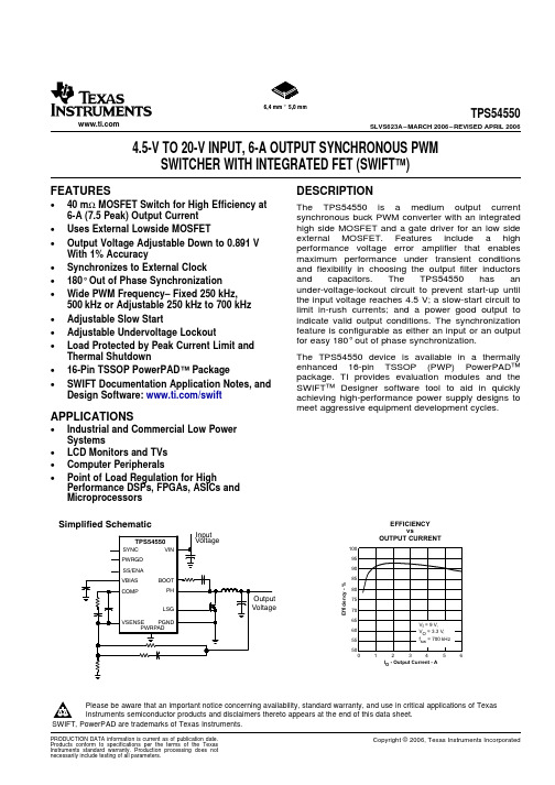
6,4 mm 55,0 mmFEATURES DESCRIPTIONAPPLICATIONSI- Output Current -AOEfficiency-%EFFICIENCYvsOUTPUT CURRENTSimplified SchematicTPS54550SLVS623A–MARCH2006–REVISED APRIL20064.5-V TO20-V INPUT,6-A OUTPUT SYNCHRONOUS PWMSWITCHER WITH INTEGRATED FET(SWIFT™)•40mΩMOSFET Switch for High Efficiency at The TPS54550is a medium output current 6-A(7.5Peak)Output Current synchronous buck PWM converter with an integratedhigh side MOSFET and a gate driver for an low side •Uses External Lowside MOSFETexternal MOSFET.Features include a high •Output Voltage Adjustable Down to0.891Vperformance voltage error amplifier that enables With1%Accuracy maximum performance under transient conditions•Synchronizes to External Clock and flexibility in choosing the output filter inductorsand capacitors.The TPS54550has an •180°Out of Phase Synchronizationunder-voltage-lockout circuit to prevent start-up until •Wide PWM Frequency–Fixed250kHz,the input voltage reaches4.5V;a slow-start circuit to500kHz or Adjustable250kHz to700kHz limit in-rush currents;and a power good output to •Adjustable Slow Start indicate valid output conditions.The synchronizationfeature is configurable as either an input or an output •Adjustable Undervoltage Lockoutfor easy180°out of phase synchronization.•Load Protected by Peak Current Limit andThe TPS54550device is available in a thermally Thermal Shutdownenhanced16-pin TSSOP(PWP)PowerPAD™•16-Pin TSSOP PowerPAD™Packagepackage.TI provides evaluation modules and the •SWIFT Documentation Application Notes,and SWIFT™Designer software tool to aid in quickly Design Software:/swift achieving high-performance power supply designs tomeet aggressive equipment development cycles.•Industrial and Commercial Low PowerSystems•LCD Monitors and TVs•Computer Peripherals•Point of Load Regulation for HighPerformance DSPs,FPGAs,ASICs andMicroprocessorsPlease be aware that an important notice concerning availability,standard warranty,and use in critical applications of TexasInstruments semiconductor products and disclaimers thereto appears at the end of this data sheet.SWIFT,PowerPAD are trademarks of Texas Instruments.PRODUCTION DATA information is current as of publication date.Copyright©2006,Texas Instruments Incorporated Products conform to specifications per the terms of the TexasInstruments standard warranty.Production processing does notnecessarily include testing of all parameters.PACKAGE DISSIPATION RATINGS (1)TPS54550SLVS623A–MARCH 2006–REVISED APRIL 2006These devices have limited built-in ESD protection.The leads should be shorted together or the device placed in conductive foam during storage or handling to prevent electrostatic damage to the MOS gates.ORDERING INFORMATIONT jOUTPUT VOLTAGE PACKAGE PART NUMBER (1)-40°C to 125°CAdjustable to 0.891VPlastic HTSSOP (PWP)TPS54550PWP (2)(1)For the most current package and ordering information,see the Package Option Addendum at the end of this document,or see the TI website at .(2)The PWP package is also available taped and reeled.Add an R suffix to the device type (i.e.,TPS54550PWPR).THERMAL IMPEDANCE T A =25°C T A =70°C T A =85°C PACKAGEJUNCTION-TO-AMBIENTPOWER RATINGPOWER RATINGPOWER RATING16-Pin PWP with solder (2)40.1°C/W2.491.371.00(1)See Figure 22for power dissipation curves.(2)Test Board Conditions a.3inch x 3inchb.Thickness:0.062inchc.2PCB layersd.2oz.Coppere.See Figure 26,Figure 27and TPS54550evaluation module user's guide for layout suggestions.2Submit Documentation FeedbackABSOLUTE MAXIMUM RATINGSELECTROSTATIC DISCHARGE RECOMMENDED OPERATING CONDITIONSTPS54550 SLVS623A–MARCH2006–REVISED APRIL2006over operating free-air temperature range unless otherwise noted(1)UNITVIN-0.3V to21.5VVSENSE-0.3V to8.0VUVLO-0.3V to8.0VV I Input voltage rangeSYNC-0.3V to4.0VSSENA-0.3V to4.0VBOOT VI(PH)+8.0VVBIAS-0.3to8.5VLSG-0.3to8.5VSYNC-0.3to4.0VV O Output voltage range RT-0.3to4.0VPWRGD-0.3to6.0VCOMP-0.3to4.0VPH-1.5V to22VPH Internally Limited(A)I O Source current LSG(Steady State Current)10mACOMP,VBIAS3mASYNC5mALSG(Steady State Current)100mAI S Sink current,PH(Steady State Current)500mACOMP3mASSENA,PWRGD10mA Voltage differential AGND to PGND±0.3VT J Junction temperature+150°CT stg Storage temperature-65°C to+150°C Lead temperature1,6mm(1/16inch)from case for10seconds260°C(1)Stresses beyond those listed under absolute maximum ratings may cause permanent damage to the device.These are stress ratingsonly,and functional operation of the device at these or any other conditions beyond those indicated under recommended operating conditions is not implied.Exposure to absolute-maximum-rated conditions for extended periods may affect device reliability.MIN TYP MAX UNIT Human Body Model HBM JESD22-A114 1.5kV Charged Device Model CDM JESD22-C101 1.5kVMIN NOM MAX UNIT V I Input voltage range 4.520VT J Operating junction temperature-40125°C3Submit Documentation FeedbackELECTRICAL CHARACTERISTICSTPS54550SLVS623A–MARCH 2006–REVISED APRIL 2006T J =-40°C to 125°C,VIN =4.5V to 20V (unless otherwise noted)PARAMETERTEST CONDITIOINSMIN TYP MAX UNITSUPPLY CURRENT Operating Current,PH pin open,10.3mA No external low side MOSFET,RT =Hi-Z I QQuiescent current Shutdown,SSENA =0V1.1mA Start threshold voltage4.324.49V VINStop threshold voltage 3.693.97V Hysteresis350mV UNDER VOLTAGE LOCK OUT (UVLO PIN)Start threshold voltage1.201.24V UVLOStop threshold voltage 1.021.10V Hysteresis100mVBIAS VOLTAGE (VBIAS PIN)I VBIAS =1mA,VIN ≥12V 7.57.88.0VBIASOutput voltageVI VBIAS =1mA,VIN =4.5V 4.4 4.47 4.5REFERENCE SYSTEM ACCURACYT J =25°C0.8880.8910.894V Reference voltage0.8820.8910.899VOSCILLATOR (RT PIN)RT Grounded 200250300Internally set PWM switching frequency kHz RT Open400500600Externally set PWM switching frequency RT =100k Ω(1%resistor to AGND)425500575kHz FALLING EDGE TRIGGERED BIDIRECTIONAL SYNC SYSTEM (SYNC PIN)SYNC out low-to-high rise time (10%/90%)(1)25pF to ground 200500ns SYNC out high-to-low fall time (90%/10%)(1)25pF to ground510ns Delay from rising edge to rising edge of Falling edge delay time (1)180°PH pins Minimum input pulsewidth (1)RT =100k Ω100ns Delay (falling edge SYNC to rising edge PH)(1)RT =100k Ω360ns 50k Ωresistor to ground,SYNC out high level voltage 2.5V No pullup resistorSYNC out low level voltage 0.6V SYNC in low level threshold 0.8V SYNC in high level threshold 2.3V Percentage of programmed frequency-10%10%SYNC in frequency range (1)225770kHz FEED-FORWARD MODULATOR (INTERNAL SIGNAL)Modulator gainVIN =12V,T J =25°C8V/VModulator gain variation -25%25%Minimum controllable ON time (1)180nsMaximum duty factor (1)VIN =4.5V80%86%ERROR AMPLIFIER (VSENSE and COMP PINS)Error amplifier open loop voltage gain (1)6080dB Error amplifier unity gain bandwidth (1) 1.02.8MHz Input bias current,VSENSE pin500nA COMPOutput voltage slew rate (symmetric)(1)1.5V/µs (1)Specified by design,not production tested.4Submit Documentation FeedbackTPS54550 SLVS623A–MARCH2006–REVISED APRIL2006ELECTRICAL CHARACTERISTICS(continued)T J=-40°C to125°C,VIN=4.5V to20V(unless otherwise noted)PARAMETER TEST CONDITIOINS MIN TYP MAX UNIT Slow Start/ENABLE(SSENA PIN)Disable low level input voltage0.5Vf s=250kHz,RT=ground(2) 4.6Internal slow-start time(10%to90%)msf s=500kHz,RT=Hi-Z(2) 2.3Pullup current source 1.8510µAPulldown MOSFET II(SSENA)=1mA0.1V POWER GOOD(PWRGD PIN)Power good threshold Rising voltage97%f s=250kHz4Rising edge delay(2)msf s=500kHz2Output saturation voltage I sink=1mA,VIN>4.5V0.05V PWRGD Output saturation voltage I sink=100µA,VIN=0V0.76V Open drain leakage current Voltage on PWRGD=6V3µA CURRENT LIMITCurrent limit VIN=12V7.58.59.5ACurrent limit Hiccup Time(2)f s=500kHz 4.5ms THERMAL SHUTDOWNThermal shutdown trip point165°CThermal shutdown hysteresis(2)7°C LOW SIDE MOSFET DRIVER(LSG PIN)VIN=4.5V,Capacitive load=1000pF15 Turn on rise time,(10%/90%)(2)nsVIN=8V,Capacitive load=1000pF12 Deadtime(2)VIN=12V60nsVIN=4.5V sink/source7.5 Driver ON resistanceΩVIN=12V sink/source5OUTPUT POWER MOSFETS(PH PIN)Phase node voltage when disabled DC conditions and no load,SSENA=0V0.5VVIN=4.5V,Idc=100mA 1.13 1.42 Voltage drop,low side FET and diode VVIN=12V,Idc=100mA 1.08 1.38VIN=4.5V,BOOT-PH=4.5V,I O=0.5A60r DS(ON)High side power MOSFET switch(3)mΩVIN=12V,BOOT-PH=8V,I O=0.5A40(2)Specified by design,not production tested.(3)Resistance from VIN to PH pins.5Submit Documentation FeedbackPIN ASSIGNMENTSVIN VIN UVLO PWRGDRT SYNC SSENA COMPBOOT PH PH LSG VBIAS PGND AGND VSENSEPWP PACKAGE (TOP VIEW)NOTE:If there is not a Pin 1 indicator, turn device to enable reading the symbol from left to right. Pin 1 is at the lower left corner of the device.TPS54550SLVS623A–MARCH 2006–REVISED APRIL 2006Terminal FunctionsTERMINAL DESCRIPTION 1,2VIN Input supply voltage,4.5V to 20V.Must bypass with a low ESR 10-µF ceramic capacitor.3UVLO Undervoltage lockout pin.Connecting an external resistive voltage divider from VIN to the pin will override the internal default VIN start and stop thresholds.4PWRGD Power good output.Open drain output.A low on the pin indicates that the output is less than the desired output voltage.There is an internal rising edge filter on the output of the PWRGD comparator.5RT Frequency setting pin.Connect a resistor from RT to AGND to set the switching frequency.Connecting the RT pin to ground or floating will set the frequency to an internally preselected frequency.6SYNCBidirectional synchronization I/O pin.SYNC pin is an output when the RT pin is floating or connected low.The output is a falling edge signal out of phase with the rising edge of PH.SYNC may be used as an input tosynchronize to a system clock by connecting to a falling edge signal when an RT resistor is used.See 180°Out of Phase Synchronization operation in the Application Information section.7SSENASlow Start/Enable.The SSENA pin is a dual function pin which provides a logic enable/disable and a slow start time set.Below 0.5V,the device stops switching.Float pin to enable.Capacitor to ground adjusts the slow start time.See Extending Slow Start Time section.8COMP Error amplifier output.Connect frequency compensation network from COMP to VSENSE pins.9VSENSE Inverting node error amplifier.10AGND Analog ground—internally connected to the sensitive analog ground circuitry.Connect to PGND and PowerPAD.11PGND Power Ground—Noisy internal ground—Return currents from the LSG driver output return through the PGND pin.Connect to AGND and PowerPAD.12VBIAS Internal 8.0V bias voltage.A 1.0µF ceramic bypass capacitance is required on the VBIAS pin.13LSG Gate drive for low side MOSFET.Connect gate of n-channel MOSFET.14,15PH Phase node—Connect to external L-C filter.16BOOT Bootstrap for high side gate driver.Connect 24Ohm and 0.1µF ceramic capacitor from BOOT to PH pins.17PowerPADPGND and AGND pins must be connected to the exposed pad for proper operation.See Figure 26for an example PCB layout.6Submit Documentation FeedbackFUNCTIONAL BLOCK DIAGRAMPHLSGPWRGDAGNDPGNDVBIASPOWERPADTPS54550SLVS623A–MARCH 2006–REVISED APRIL 20067Submit Documentation FeedbackDETAILED DESCRIPTIONUndervoltage Lockout(UVLO)Slow Start Enable(SSENA)and Internal SlowT SS_INTERNAL(ms) 1.15kƒs(kHz)(3)Input Voltage SupplyExtending Slow Start TimeR1 VIN(start)1k p1.24V)1k p(1)VIN(stop) (R1)1k p) 1.02V1k p(2)TPS54550SLVS623A–MARCH2006–REVISED APRIL2006StartThe undervoltage lockout(UVLO)system has aninternal voltage divider from VIN to AGND.The Once the SSENA pin voltage exceeds0.5V,the defaults for the start/stop values are labeled VIN and TPS54550starts operation.The TPS54550has an given in Table1.The internal UVLO threshold can be internal digital slow start that ramps the reference overridden by placing an external resistor divider from voltage to its final value in1150switching cycles.The VIN to ground.The internal divider values are internal slow start time(10%-90%)is approximated approximately320kΩfor the high side resistor and by the following expression:125kΩfor the low side resistor.The divider ratio(andtherefore the default start/stop values)is quiteaccurate,but the absolute values of the internalresistors may vary as much as15%.If high accuracy Once the TPS54550device is in normal regulation, is required for an externally adjusted UVLO threshold,the SSENA pin is high.If the SSENA pin is pulled select lower value external resistors to set the UVLO below the stop threshold of0.5V,switching stops ing a1-kΩresistor for the low side and the internal slow start resets.If an application resistor R2(see Figure1)is recommended.Under no requires the TPS54550to be disabled,use open circumstances should the UVLO pin be connected drain or open collector output logic to interface to the directly to VIN.SSENA pin(see Figure2).The SSENA pin has aninternal pullup current source.Do not use external Table1.Start/Stop Voltage Threshold pullup resistors.START VOLTAGE STOP VOLTAGETHRESHOLD THRESHOLDVIN(Default) 4.49 3.69UVLO 1.24 1.02Figure2.Interfacing to the SSENA Pin Figure1.Circuit Using External UVLO FunctionThe equations for selecting the UVLO resistors are:In applications that use large values of outputcapacitance there may be a need to extend the slowstart time to prevent the startup current from trippingthe current limit.The current limit circuit is designedto disable the high side MOSFET and reset theinternal voltage reference for a short amount of time For applications which require an undervoltage lockwhen the high side MOSFET current exceeds the out(UVLO)threshold greater than4.49V,externalcurrent limit threshold.If the output capacitance and resistors may be implemented,see Figure1,to adjustload current cause the startup current to exceed the the start voltage threshold.For example,ancurrent limit threshold,the power supply output will application needing an UVLO start voltage ofnot reach the desired output voltage.To extend the approximately7.8V using the equation(1),R1isslow start time and to reduce the startup current,an calculated to the nearest standard resistor value ofexternal capacitor can be added to the SSENA pin.5.36kΩ.Using Equation2,the input voltage stopThe slow start capacitance is calculated using the threshold is calculated as6.48V.following equation:C SS(µF)=5.55x10⁻³T ss(ms)8Submit Documentation FeedbackSwitching Frequency(RT)RT(k p)46000ƒs(kHz)–35.9(4)V I(SYNC) V O(PH)TPS54550 SLVS623A–MARCH2006–REVISED APRIL2006The TPS54550has an internal oscillator thatoperates at twice the PWM switching frequency.TheThe RT pin controls the SYNC pin functions.If the RT internal oscillator frequency is controlled by the RTpin is floating or grounded,SYNC is an output.If the pin.Grounding the RT pin sets the PWM switchingswitching frequency has been programmed using a frequency to a default frequency of250kHz.Floatingresistor from RT to AGND,then SYNC functions as the RT pin sets the PWM switching frequency toan input.500kHz.The internal voltage ramp charging current increases Connecting a resistor from RT to AGND sets thelinearly with the set frequency and keeps the feed frequency according to Equation4(see Figure13).forward modulator constant(Km=8)regardless ofthe frequency set point.Table2.Switching Frequency,SYNC and RT PinsSWITCHING FREQUENCY SYNC PIN RT PIN250kHz,internally set Generates SYNC output signal AGND500kHz,internally set Generates SYNC output signal Float Externally set to250kHz to700kHz Terminate to quiet ground with10-kΩR=215kΩto69kΩresistor.Externally synchronized frequency Synchronization Signal Use110kΩwhen RT floats and237kΩwhen RT isgrounded and using the sync out signal of anotherTPS54550.Set RT resistor equal to90%to110%ofexternal synchronization frequency.180°Out of Phase Synchronization(SYNC)When operating the two TPS54550devices180°outof phase,the total RMS input current is reduced. The SYNC pin is configurable as an input or as an Thus reducing the amount of input capacitance output,per the description in the previous section.needed and increasing efficiency.When operating as an input,the SYNC pin is afalling-edge triggered signal(see Figure3and When synchronizing a TPS54550to an external Figure4).When operating as an output,the signal's signal,the timing resistor on the RT pin must be set falling edge is approximately180°out of phase with so that the oscillator is programmed to run at90%to the rising edge of the PH pins.Thus,two TPS54550110%of the synchronization frequency.devices operating in a system can share an inputNOTE:Do not use synchronization input for designs capacitor and draw ripple current at twice thewith output voltages>10V.frequency of a single unit.Figure3.SYNC Input Waveform9Submit Documentation FeedbackInternal OscillatorV O(PH)V O(SYNC)Power Good (PWRGD)Bootstrap Voltage (BOOT)Error AmplifierVoltage ReferenceT delay 1000ƒs(kHz)ms (5)Bias Voltage (VBIAS)TPS54550SLVS623A–MARCH 2006–REVISED APRIL 2006Figure 4.SYNC Output WaveformUp to 1mA of current can be drawn for use in anexternal application circuit.The VBIAS pin must have a bypass capacitor value of 1.0µF.X7R or X5R The VSENSE pin is compared to an internal grade dielectric ceramic capacitors are recommended reference signal,if the VSENSE is greater than 97%because of their stable characteristics over and no other faults are present,the PWRGD pin temperature.presents a high impedance.A low on the PWRGD pin indicates a fault.The PWRGD pin has been designed to provide a weak pull-down and indicates a fault even when the device is unpowered.If the TPS54550The BOOT capacitor obtains its charge cycle by cycle has power and has any fault flag set,the TPS54550from the VBIAS capacitor.A capacitor and small indicates the power is not good by driving the value resistor from the BOOT pin to the PH pins is PWRGD pin low.The following events,singly or in required for operation.The bootstrap connection for combination,indicate power is not good:the high side driver must have a bypass capacitor of 0.1µF and resistor 24Ohm.•VSENSE pin out of bounds •Overcurrent•Thermal shutdown The VSENSE pin is the error amplifier inverting input.•UVLO undervoltageThe error amplifier is a true voltage amplifier with 1.5•Input voltage not present (weak pull-down)mA of drive capability with a minimum of 60dB of •Slow-startingopen loop voltage gain and a unity gain bandwidth of •VBIAS voltage is low2MHz.Once the PWRGD pin presents a high impedance (i.e.,power is good),a VSENSE pin out of bounds condition forces PWRGD pin low (i.e.,power is bad)The voltage reference system produces a precision after a time delay.This time delay is a function of the reference signal by scaling the output of a switching frequency and is calculated using temperature stable bandgap circuit.During production Equation 5:testing,the bandgap and scaling circuits are trimmed to produce 0.891V at the output of the error amplifier,with the amplifier connected as a voltage follower.The trim procedure improves the regulation,since it cancels offset errors in the scaling and error amplifier circuits.The VBIAS regulator provides a stable supply for the internal analog circuits and the low side gate driver.10Submit Documentation FeedbackPWM Control and Feed ForwardDeadtime ControlLow Side Gate Driver(LSG)Thermal Shutdown TPS54550SLVS623A–MARCH2006–REVISED APRIL2006reference ramps from0V to0.891V.During theinitial slow-start interval,the internal reference voltage Signals from the error amplifier output,oscillator,and is very small resulting in a couple of skipped pulses current limit circuit are processed by the PWM control because the minimum on time causes the actual logic.Referring to the internal block diagram,the output voltage to be slightly greater than the preset control logic includes the PWM comparator,PWM output voltage until the internal reference ramps up. latch,and the adaptive dead-time control logic.During steady-state operation below the current limitthreshold,the PWM comparator output and oscillatorpulse train alternately reset and set the PWM latch.Adaptive dead time control prevents shoot throughcurrent from flowing in the integrated high-side Once the PWM latch is reset,the low-side driver andMOSFET and the external low-side MOSFET during integrated pull-down MOSFET remain on for athe switching transitions by actively controlling the minimum duration set by the oscillator pulse width.turn on times of the drivers.The high-side driver does During this period,the PWM ramp discharges rapidlynot turn on until the voltage at the gate of the to the valley voltage.When the ramp begins tolow-side MOSFET is below1V.The low-side driver charge back up,the low-side driver turns off and thedoes not turn on until the voltage at the gate of the high-side FET turns on.The peak PWM ramp voltagehigh-side MOSFET is below1V.varies inversely with input voltage to maintain aconstant modulator and power stage gain of8V/V.As the PWM ramp voltage exceeds the error amplifierLSG is the output of the low-side gate driver.The output voltage,the PWM comparator resets the latch,100-mA MOSFET driver is capable of providing gate thus turning off the high-side FET and turning on thedrive for most popular MOSFETs suitable for this low-side FET.The low-side driver remains on untile the SWIFT Designer Software Tool the next oscillator pulse discharges the PWM ramp.to find the most appropriate MOSFET for the During transient conditions,the error amplifier output application.Connect the LSG pin directly to the gate can be below the PWM ramp valley voltage or above of the low-side MOSFET.Do not use a gate resistor the PWM peak voltage.If the error amplifier is high,as the resulting turn-on time may be too slow.the PWM latch is never reset and the high-side FETremains on until the oscillator pulse signals thecontrol logic to turn the high-side FET off and theThe device uses the thermal shutdown to turn off the internal low-side FET and driver on.The deviceMOSFET drivers and controller if the junction operates at its maximum duty cycle until the outputtemperature exceeds165°C.The device is restarted voltage rises to the regulation set point,settingautomatically when the junction temperature VSENSE to approximately the same voltage as thedecreases to7°C below the thermal shutdown trip internal voltage reference.If the error amplifier outputpoint and starts up under control of the slow-start is low,the PWM latch is continually reset and thecircuit.high-side FET does not turn on.The internal low-sideFET and low side driver remain on until the VSENSEvoltage decreases to a range that allows the PWMcomparator to change states.The TPS54550iscapable of sinking current through the external lowside FET until the output voltage reaches theregulation set point.The minimum on time is designed to be180ns.During the internal slow-start interval,the internalOvercurrent ProtectionOutput Voltage LimitationsT HICCUP(ms) 2250ƒs(kHz)(6)Setting the Output VoltageR2 R1 0.891V O )0.891(7)TPS54550SLVS623A–MARCH 2006–REVISED APRIL 2006OUTPUT VOLTAGE (V)R2VALUE (k Ω)1.228.7Overcurrent protection is implemented by sensing the 1.514.7drain-to-source voltage across the high-side 1.89.76MOSFET and compared to a voltage level which represents the overcurrent threshold limit.If the2.5 5.49drain-to-source voltage exceeds the overcurrent3.33.74threshold limit for more than 100ns,the high-side MOSFET is disable,the SSENA pin is pulled low,and the internal digital slow-start is reset to 0V.SSENA is held low for approximately the time that is calculated Due to the internal design of the TPS54550there are by Equation 6:both upper and lower output voltage limits for any given input voltage.Additionally,the lower boundary of the output voltage set point range is also dependent on operating frequency.The upper limit of the output voltage set point is constrained by the Once the hiccup time is complete,the SSENA pin ismaximum duty cycle of the device and is shown in released and the converter initiates the internal Figure 12.The lower limit is constrained by the slow-start.minimum controllable on time which may be as high as 220ns.The approximate minimum output voltage for a given input voltage and range of operating The output voltage of the TPS54550can be set by frequencies is shown in Figure 8while the maximum feeding back a portion of the output to the VSENSE operating frequency versus input voltage for some pin using a resistor divider network.In the application common output voltages is shown in Figure 10.circuit of Figure 29,this divider network is comprised The curves shown in these two figures are valid for of resistors R1and R2.To calculate the resistor output currents greater than 0.5A.As output currents values to generate the required output voltage use decrease towards no load (0A),the minimum output the following equation:voltage decreases.For applications where the load current is less than 100mA,the curves shown in Figure 9and Figure 11are applicable.All of the data plotted in these curves are approximate and take into Start with a fixed value of R1and calculate theaccount a possible 20percent deviation in actual required R2value.Assuming a fixed value of 10k Ωoperating frequency relative to the intended set point.for R1,the following table gives the appropriate R2value for several common output voltages:TYPICAL CHARACTERISTICS0102030405060708090T - Junction Temperature - °CJ O n R e s i s t a n c e - m W0.89120.89100.89080.89060.89040.89020.89000.8898−50−250255075100125150V r e f − I n t e r n a l V o l t a g e R e f e r e n ce − VT J − Junction Temperature − 5CV - Input Voltage - VI C u r r e n t L i m i t -AM i n i m u m O u t p u t V o l t a g e − VV I − Input Voltage − V100200300400500600700800M a x i m u m S w i t c h i n g F r e q u e n c y − k H zV I − Input Voltage − VM i n i m u m O u t p u t V o l t a g e − VV I − Input Voltage − VM a x i m u m S w i t c h i n g F r e q u e n c y − k H zV I − Input Voltage − V5075100125150175200225200300400500600700R T R e s i s t a n c e − k WSwitching Frequency − kHz02468101214510152025− O u t p u t V o l t a g e − VV O V I − Input Voltage − VTPS54550SLVS623A–MARCH 2006–REVISED APRIL 2006ON RESISTANCECURRENT LIMITINTERNAL VOLTAGE REFERENCEvsvsvsJUNCTION TEMPERATUREINPUT VOLTAGEJUNCTION TEMPERATUREFigure 5.Figure 6.Figure 7.MINIMUM OUTPUT VOLTAGEMINIMUM OUTPUT VOLTAGEMAXIMUM SWITCHING FREQUENCYvsvsvsINPUT VOLTAGEINPUT VOLTAGEINPUT VOLTAGEFigure 8.Figure 9.Figure 10.MAXIMUM SWITCHING FREQUENCYMAXIMUM OUTPUT VOLTAGERT RESISTANCEvsvsvsINPUT VOLTAGEINPUT VOLTAGESWITCHING FREQUENCYFigure 11.Figure 12.Figure 13.。

1D Precision Programmable Reference (2.5 V)and an Optocoupler in a Single Package D Reference Voltage Tolerance – TPS59040.8%– TPS5904A 0.5%D Controlled Optocoupler CTRs:– TPS5904100% to 400%– TPS5904A 150% to 300%D High Withstand Voltage (WTV), 7500 V Peak for 1 MinuteDSafety Regulatory Approvals Pending – UL– FIMKO, SEMKO, NEMKO, DEMKO – EN60065/IEC 65– EN60950/IEC 950– VDE 0884, Level 4 (6000-V Insulation)DescriptionThe TPS5904 and TPS5904A optoisolated feedback amplifiers consist of a precision programmable reference and an optocoupler. Reference-voltage tolerance for the TPS5904 is 0.8%, and for the TPS5904A is 0.5%.These devices are primarily intended for use as the error-amplifier/reference/isolation-amplifier element in isolated ac-to-dc power supplies and dc/dc converters. The optocoupler is a gallium-arsenide (GaAs)light-emitting diode that emits at a wavelength of 940 nm, combined with a silicon phototransistor. The current transfer ratio (CTR) ranges from 100% to 400% in the standard version. The TPS5904A version with a 150%-to-300% CTR is available for higher-performance applications. When using the TPS5904 or TPS5904A,power supply designers can reduce component count and save space in tightly packaged designs. The tight-tolerance reference eliminates the need for adjustments in many applications.Copyright © 2000, TAOS Inc.LED COMP GND FBNC C E NCDCS OR P PACKAGE(TOP VIEW)NC – No internal connection2ttFunctional Block DiagramLEDCOMPFB GNDCETerminal FunctionsAbsolute Maximum Ratings at 25°C free-air temperature (unless otherwise noted)†Input power dissipation at (or below) T A = 25°C (see Note 1) 250 mW . . . . . . . . . . . . . . . . . . . . . . . . . . . . . . . . . Input LED current, I I(LED) 50 mA . . . . . . . . . . . . . . . . . . . . . . . . . . . . . . . . . . . . . . . . . . . . . . . . . . . . . . . . . . . . . . . . . Input LED voltage, V I(LED) 37 V . . . . . . . . . . . . . . . . . . . . . . . . . . . . . . . . . . . . . . . . . . . . . . . . . . . . . . . . . . . . . . . . . . Input diode reverse voltage 6 V . . . . . . . . . . . . . . . . . . . . . . . . . . . . . . . . . . . . . . . . . . . . . . . . . . . . . . . . . . . . . . . . . . Output power dissipation at (or below) T A = 25°C (see Note 2) 150 mW . . . . . . . . . . . . . . . . . . . . . . . . . . . . . . . . Output collector-to-emitter voltage 35 V . . . . . . . . . . . . . . . . . . . . . . . . . . . . . . . . . . . . . . . . . . . . . . . . . . . . . . . . . . . Output emitter-to-collector voltage 7 V . . . . . . . . . . . . . . . . . . . . . . . . . . . . . . . . . . . . . . . . . . . . . . . . . . . . . . . . . . . . Output collector current 50 mA . . . . . . . . . . . . . . . . . . . . . . . . . . . . . . . . . . . . . . . . . . . . . . . . . . . . . . . . . . . . . . . . . . Total continuous power dissipation at (or below) T A = 25°C (see Note 3) 350 mW . . . . . . . . . . . . . . . . . . . . . . . Operating free-air temperature range, T A –40°C to 100°C . . . . . . . . . . . . . . . . . . . . . . . . . . . . . . . . . . . . . . . . . . . Storage temperature range, T stg –55°C to 150°C . . . . . . . . . . . . . . . . . . . . . . . . . . . . . . . . . . . . . . . . . . . . . . . . . . . Total input-to-output voltage 7.5 kV peak or dc (5.3 kVrms). . . . . . . . . . . . . . . . . . . . . . . . . . . . . . . . . . . . . . . . . . Lead temperature 1,6 mm (1/16 inch) from case for 10 seconds 260°C . . . . . . . . . . . . . . . . . . . . . . . . . . . . . . . Flammability (see Note 4). . . . . . . . . . . . . . . . . . . . . . . . . . . . . . . . . . . . . . . . . . . . . . . . . . . . . . . . . . . . . . . . . . . . . . . †Stresses beyond those listed under “absolute maximum ratings” may cause permanent damage to the device. These are stress ratings only, and functional operation of the device at these or any other conditions beyond those indicated under “recommended operating conditions” is not implied. Exposure to absolute-maximum-rated conditions for extended periods may affect device reliability.NOTES: 1.Derate linearly from 25°C at a rate of 2.95 mW/°C.2.Derate linearly from 25°C at a rate of 1.76 mW/°C.3.Derate linearly from 25°C at a rate of4.12 mW/°C.4.Optocoupler total-package flame retardancy is tested to IEC695-2-2 using a flame application time of 30 seconds. Outer moldcompound is verified to meet UL 94V-0.TAOS017 – SEPTEMBER 19993ttElectrical Characteristics, T A = 25°C (unless otherwise noted)This symbol is not currently listed within EIA or JEDEC standards for semiconductor symbology.OutputCouplerTAOS017 – SEPTEMBER 19994ttPARAMETER MEASUREMENT INFORMATIONIFigure 1. V ref, V F, I min Test CircuitVFigure 2. ∆V ref/∆V I(LED) Test CircuitVFigure 3. I I(FB) Test CircuitVFigure 4. I I(off) Test CircuitVFigure 5. I CEO Test Circuit Figure 6. CTR, V CE(sat) Test CircuitVITAOS017 – SEPTEMBER 19995ttTYPICAL CHARACTERISTICSFigure 7600400200000.51– I n p u t L i g h t -E m i t t i n g -D i o d e C u r r e n t –8001200INPUT LIGHT-EMITTING-DIODE CURRENTvsREFERENCE VOLTAGE14001.522.53AµI V ref– Reference Voltage – VI (L E D )Figure 8302010000.514050INPUT LIGHT-EMITTING-DIODE CURRENTvsREFERENCE VOLTAGE601.522.53V ref– Reference Voltage – V– I n p u t L i g h t -E m i t t i n g -D i o d e C u r r e n t – m AI I (L E D )Figure 92.52.492.482.47– 50– 250– R e f e r e n c e V o l t a g e – V2.512.52REFERENCE VOLTAGEvsFREE-AIR TEMPERATURE2.53255075100r e f V T A – Free-Air Temperature – °CFigure 10– 1.15– 1.25– 1.35– 1.45– 50– 250– R a t i o o f D e l t a R e f e r e n c e V o l t a g e – 1.05– 0.95RATIO OF DELTA REFERENCE VOLTAGE TO DELTA LED VOLTAGEvsFREE-AIR TEMPERATURE255075100T A – Free-Air Temperature – °Ct o D e l t a L E D V o l t a g e – VI (L E D )TAOS017 – SEPTEMBER 19996ttTYPICAL CHARACTERISTICSFigure 111.510.5– 25022.5REFERENCE CURRENTvsFREE-AIR TEMPERATURE255075100T A – Free-Air Temperature – °C–ReferenceCurrent–AµIIFigure 120.150.10.05– 2500.20.25OFF-STATE INPUTLIGHT-EMITTING-DIODE CURRENTvsFREE-AIR TEMPERATURE255075100T A – Free-Air Temperature – °C–Off-StateInputLight-Emitting-DiodeI(off)IAµ– 50Current–Figure 130.1– 250COLLECTOR DARK CURRENTvsFREE-AIR TEMPERATURE255075100T A – Free-Air Temperature – °C–CollectorDarkCurrent–nACEOI– 50100101100010000Figure 140.60.40.2– 50– 250CTR–NormalizedCurrentTransferRatio0.81NORMALIZED CURRENT TRANSFER RATIORELATIVE TO VALUE AT T A = 25°CvsFREE-AIR TEMPERATURE1.2255075100T A – Free-Air Temperature – °CRelativetoValueatTA=25C°TAOS017 – SEPTEMBER 19997ttTYPICAL CHARACTERISTICSFigure 15150100500300125102030C T R – C u r r e n t T r a n s f e r R a t i o – %250200CURRENT TRANSFER RATIOvsINPUT LIGHT-EMITTING-DIODE CURRENT503I I(LED)– Input Light-Emitting-Diode Current – mAFigure 160.140.120.100.08– 50– 250– C o l l e c t o r -t o -E m i t t e r S a t u r a t i o n V o l t a g e – V0.160.18COLLECTOR-TO-EMITTER SATURATION VOLTAGEvsFREE-AIR TEMPERATURE0.20255075100C E (s a t )V T A – Free-Air Temperature – °C30201000.80.914050INPUT LIGHT-EMITTING-DIODE FORWARD CURRENTvsLIGHT-EMITTING-DIODE FORWARD VOLTAGE601.1 1.2 1.3 1.4V F – Light-Emitting-Diode Forward Voltage – V– I n p u t L i g h t -E m i t t i n g -D i o d e F o r w a r d C u r r e n t – m AI (L E D )I Figure 17TAOS017 – SEPTEMBER 19998tt MECHANICAL DATADCS PLASTIC DUAL SMALL-OUTLINE OPTO COUPLERNOTES: A.All linear dimensions are in inches(millimeters).B.This drawing is subject to change without notice.TAOS017 – SEPTEMBER 19999ttMECHANICAL DATAPPLASTIC DUAL-IN-LINE PACKAGENOTES: A.All linear dimensions are in inches (millimeters).B.This drawing is subject to change without notice.C.Falls within JEDEC MS-001TAOS017 – SEPTEMBER 199910ttPRODUCTION DATA — information in this document is current at publication date. Products conform to specifications in accordance with the terms of Texas Advanced Optoelectronic Solutions, Inc. standard warranty. Production processing does not necessarily include testing of all parameters.NOTICETexas Advanced Optoelectronic Solutions, Inc. (TAOS) reserves the right to make changes to the products contained in this document to improve performance or for any other purpose, or to discontinue them without notice. Customers are advised to contact TAOS to obtain the latest product information before placing orders or designing TAOS products into systems. TAOS assumes no responsibility for the use of any products or circuits described in this document or customer product design, conveys no license, either expressed or implied, under any patent or other right, and makes no representation that the circuits are free of patent infringement. TAOS further makes no claim as to the suitability of its products for any particular purpose, nor does TAOS assume any liability arising out of the use of any product or circuit, and specifically disclaims any and all liability, including without limitation consequential or incidental damages.TEXAS ADVANCED OPTOELECTRONIC SOLUTIONS, INC. PRODUCTS ARE NOT DESIGNED OR INTENDED FOR USE IN CRITICAL APPLICATIONS IN WHICH THE FAILURE OR MALFUNCTION OF THE TAOS PRODUCT MAY RESULT IN PERSONAL INJURY OR DEATH. USE OF TAOS PRODUCTS IN LIFE SUPPORT SYSTEMS IS EXPRESSLY UNAUTHORIZED AND ANY SUCH USE BY A CUSTOMER IS COMPLETELY AT THE CUSTOMER’S RISK.。

Parameter 参数Symbol 符号Conditions 条件最小. 典型. 最大. 单位Output Voltage 输出电压VO TJ=+25℃- 8.7 - 9.0 - 9.3 VIO = 5mA to 1A, PO ≤15W VI = -1.5V to -23V - 8.6 - 9.0 - 9.4Line Regulation 线性调整率(Note1) ΔVO TJ=+25℃VI = -10.5V to -25V - 10 180 mVVI = -11V to -17V - 5 90Load Regulation 负载调整率(Note1) (Note1) ΔVO TJ=+25℃IO = 5mA to 1.5A - 12 180 mVTJ =+25℃IO = 250mA to 750mA - 4 90Quiescent Current 静态电流IQ TJ =+25℃- 3 6 mAQuiescent Current Change 静态电流变化ΔIQ IO = 5mA to 1A - 0.05 0.5 mAVI = -11.5V to -25V - 0.1 1Temperature Coefficient of VD 温度系数ΔV o/ΔT IO = 5mA - -0.6 - mV/℃Output Noise Voltage 输出噪声电压VN f = 10Hz to 100KHz TA =+25℃- 175 - μV Ripple Rejection 纹波抑制RR f = 120Hz ΔVI = 10V 54 60 - dBDropout V oltage 电压差VD TJ=+25℃IO = 1A - 2 - VShort Circuit Current 短路电流ISC TJ =+25℃, VI = -35V - 300 - mAPeak Current 峰值电流IPK TJ =+25℃- 2.2 - A三端稳压集成电路极限参数:Parameter 参数Symbol 符号Value 单位Input V oltage输入电压(for VO =5V to 18V) VI 35 V(for VO =24V) VI 40 VThermal Resistance Junction-Cases 热阻(结到壳) (TO-220) RθJC 5 ℃/WThermal Resistance Junction-Air热阻(结到空气) (TO-220) RθJA 65 ℃/WOperating Temperature Range工作温度范围TOPR 0 ~ +125 ℃Storage Temperature Range储存温度范围TSTG -65 ~ +150 ℃图1 79XX内部电路图图2 外形引脚排列图管脚图图3 79XX参照测试电路及典型电路图4 输出电压图5 负载调节率曲线图图6 电压差曲线图图7 静态电流曲线图。

概述HJ12864M-1是一款图形点阵液晶显示器,显示分辨率为128X64。
内置中文字库,总共提供8192个16X16点阵的汉字和128个16X8点阵的字符.它可以提供三种传输模式,分别是8位并行模式、4位并行模式和串行模式。
外形尺寸项目尺寸单位mm mm mm mm93X70X1372X400.52X0.520.48X0.48模块体积视域尺寸点距离点尺寸HJ12864M-1 1/9图形点阵液晶显示器说明书模块接口定义并行模式接口定义串行模式接口定义片选端,高电平有效串行数据输入端CLK 串行同步时钟CS SID H/L 电源负极电源正极对比度调节0V +5V _123VSS VDD V0引脚号电平功能说明名称H/L H/L 背光电源正极19A 背光电源负极20K+5V 0VPSB=H :并行模式 PSB=L :串行模式15PSB H/L 复位端,低电平有效17/RESETH/L 456HJ12864M-1功能说明系统界面配合RS和RW可选择控制界面的4种模式:RS RW功能说明L L MPU写指令到指令暂存器(IR)L H读出忙标志(BF)及地址计数器(AC)的状态H L MPU写数据到数据暂存器(DR)H H MPU从数据暂存器(DR)中读出数据忙标志(BF)BF标志提供内部工作情况,BF=1表示模块在进行内部操作,此时模块不接受外部指令和数据;BF=0,表示模块为准备状态,可接受外部指令和数据。
利用STATUS RD 指令,可以将BF读到DB7总线 ,从而检验模块的工作状态。
地址计数器(AC)地址计数器(AC)用来存储DDRAM/CGRAM/GDRAM之一的地址,可由指令改变,之后读取或写入DDRAM/CGRAM/GDRAM的值时,地址计数器(AC)的值就会自动加1。
当RS=0,RW=1和RE=1时,地址计数器(AC)的值将被读到DB6-DB0中。
中文字型ROM(CGROM)和半宽字型ROM(HCGROM)字型产生ROM提供8192个中文字型和128个数字符号,利用两个字节将字型编码写入DDRAM,对应的内容将显示出来。

宽电压四位数码管显示模块产品使用手册【简要说明】功能描述:此工业级板的作用是,用以显示四位数码管数值,输入低电平为有效信号,可以与单片机、PLC、工控板等可编程设备连接使用,输入电压范围广,数码管是动态扫描显示。
板子尺寸:长72mmX宽63mmX高12mm二、主要器件:数码管、译码器、稳压器三、工作电压:DC5~36V四、板子功耗:小于400mA五、特点:1、输入采用端子螺旋压接。
2、四位数码管动态扫描显示。
3、工作电压范围广5~36V。
4、输入口可以和单片机IO口直接连接无需驱动。
5、工作稳定,功耗低。
6、输入电压端具有防接反功能,电源接反不会烧坏板子。
7、可以和72MM卡槽板配合安装在DIN导轨上。
【标示说明】【接线说明】【真值表说明】【单片机应用例程】应用接线图/********************************************************************汇诚科技实现功能:宽电压四位数码管显示模块测试例程使用芯片:STC89C52RC晶振:12MHZ编译环境:Keil作者:zhangxinchunleo网站:淘宝店:汇诚科技【声明】此程序仅用于学习与参考,引用请注明版权和作者信息!显示效果:四位数码管分别显示1358*********************************************************************/#include<reg52.h> //库文件#define uchar unsigned char//宏定义无符号字符型#define uint unsigned int //宏定义无符号整型/********************************************************************初始定义*********************************************************************/code uchar seg7code[10]={ 0xF0,0xFE,0xFD,0xFC,0xFB,0xFA,0xF9,0xF8,0xF7,0xF6}; //显示段码数码管字跟uchar wei[4]={0XEf,0XDf,0XBf,0X7f}; //位的控制端/********************************************************************延时函数*********************************************************************/void delay(uchar t){uchar i,j;for(i=0;i<t;i++){for(j=13;j>0;j--);{ ;}}}/********************************************************************显示函数*********************************************************************/void Led(int date) //显示函数{/*****************数据转换*****************************/uint z,x,c,v;z=date/1000; //求千位x=date%1000/100; //求百位c=date%100/10; //求十位v=date%10; //求个位P2=0XFF;P0=seg7code[z];P2=wei[0];delay(80);P2=0XFF;P0=seg7code[x];P2=wei[1];delay(80);P2=0XFF;P0=seg7code[c];P2=wei[2];delay(80);P2=0XFF;P0=seg7code[v];P2=wei[3];delay(80);P2=0XFF;}/********************************************************************主函数*********************************************************************/ void main(){{int display_date=1358; //定义并赋值要显示的数据while(1){Led(display_date);//调用显示函数显示数据display_date}}}/********************************************************************结束*********************************************************************/ 【原理图】【元件清单】【PCB图】【实物图片展示】【模块加装壳体效果图】。


STD790AMEDIUM CURRENT, HIGH PERFORMANCE,LOW VOLTAGE PNP TRANSISTORsVERY LOW COLLECTOR TO EMITTER SATURATION VOLTAGEs DC CURRENT GAIN, h FE > 100s 3 A CONTINUOUS COLLECTOR CURRENT s 60 V BREAKDOWN VOLTAGE (V (BR)CER )sSURFACE MOUNTING DPAK (TO-252)POWER PACKAGE IN TAPE & REEL (Suffix "T4")APPLICATIONS s SWITCHING REGULATOR IN BATTERY CHARGER APPLICATIONS s SUITABLE FOR AUTOMOTIVE APPLICATIONS (V (BR)CER > 60V)s VOLTAGE REGULATION IN BIAS SUPPLY CIRCUITSs HEAVY LOAD DRIVERDESCRIPTION The device is manufactured in low voltage PNP Planar Technology by using a "Base Island"layout.The resulting Transistor shows exceptional high gain performance coupled with very low saturation voltage.March 2003ABSOLUTE MAXIMUM RATINGS®1/6STD790ATHERMAL DATAC unless otherwise specified)ELECTRICAL CHARACTERISTICS (T case = 25 oSwitching Times Resistive LoadSwitching Times Resistive LoadCollector-Emitter Saturation Voltage Base-Emitter Saturation VoltageDC Current GainDC Current GainSTD790ASTD790AFigure 1:Resistive Load Switching Test Circuit.STD790AInformation furnished is believed to be accurate and reliable. However, STMicroelectronics assumes no responsibility for the consequences of use of such information nor for any infringement of patents or other rights of third parties which may result from its use. No license is granted by implication or otherwise under any patent or patent rights of STMicroelectronics. Specification mentioned in this publication are subject to change without notice. This publication supersedes and replaces all information previously supplied. STMicroelectronics products are not authorized for use as critical components in life support devices or systems without express written approval of STMicroelectronics.The ST logo is a trademark of STMicroelectronics © 2003 STMicroelectronics – Printed in Italy – All Rights ReservedSTMicroelectronics GROUP OF COMPANIESAustralia - Brazil - Canada - China - Finland - France - Germany - Hong Kong - India - Israel - Italy - Japan - Malaysia - Malta - Morocco - Singapore - Spain - Sweden - Switzerland - United Kingdom - United States.STD790A。

IR 090热阴极电离复合真空计使用说明书BG 804 171 BE目录产品标识有效范围使用范围工作原理注册商标1 安全1.1 使用符号1.2 人员素质1.3 一般安全规则1.4 赔偿责任与保修2 技术参数3 安装3.1 真空连接3.1.1 拆卸和安装电子学单元3.1.2 安装延伸件3.2 电源连接3.2.1 与COMBIV AC IT23一起使用3.2.2 与其它测量仪器一起使用4 运行4.1 测量原理,测量特性4.2 真空计工作原理4.3 除气4.4 显示器4.5 RS232C接口4.5.1 功能说明4.5.1.1 IR090输出4.5.1.2 IR090输入5 维护5.1 维护5.2 真空计调整5.3 真空计清洗5.4 安装障板5.5 更换障板5.6 更换规管5.7 故障查找6 拆卸7 产品返修8 附件9 备件10 废物处理附录A. 测量讯号与压强的关系B. 气体种类与压强的关系污染申报表参阅本说明书中的章节,采用符号(→XY)。
参阅其它文献,采用符号(→[Z])。
产品标识与Leybold Inficon联系时,请标明产品标牌上给出的信息。
将信息复制在标牌的复印件上。
有效范围本说明书适用于下列件号的产品不带显示器120 90 (法兰DN 25 ISO-KF)120 92 (法兰DN 40 CF-R)带显示器120 91 (法兰DN 25 ISO-KF)120 94 (法兰DN 40 CF-R)产品的件号在标牌上标明。
本公司保留对说明书不预先通知的技术更改权。
使用范围I R090用于在压强5×10⁻¹⁰…1000毫巴范围内非易燃性气体和气体混合物的真空测量。
真空计规管是SKY Smart真空计规管系列的一个组成部分。
可与COMBIV AC IT23或其它测量仪器一起工作。
工作原理在整个测量范围内,热阴极电离复合真空计有连续的测量特性。
它的测量讯号是对数压强输出。
真空计的功能包括BA规热阴极电离测量系统(用于p<2.0×10⁻²毫巴)和皮拉尼测量系统(用于p>5.5×10⁻³毫巴)。

3,0 mm X 4,88 mmActual Size12345109876EN VREF PROG TIMER GNDVCC SENSE GATE OUT PGDGS Package (Top View)M1I V P Programmed SOA, 16mSTPS2490TPS2491SLVS503–NOVEMBER 2003POSITIVE HIGH-VOLTAGE POWER-LIMITING HOTSWAP CONTROLLERFEATURESAPPLICATIONS•Server Backplanes•Programmable Power Limiting and Current Limiting for Complete SOA Protection •Storage Area Networks (SAN)•Medical Systems •Wide Operating Range:+9V to +80V•Plug-in Modules •Latched Operation (TPS2490)and Automatic •Base StationsRetry (TPS2491)•High-side Drive for Low-R DS(on)External N-channel MOSFET•Programmable Fault Timer to Protect the MOSFET and Eliminate Nuisance Shutdowns •Power Good Open-Drain Output for Down-stream DC/DC Coordination•Enable can be used as a Programmable Undervoltage Lockout or Logic Control •Small,Space-saving 10-pin MSOP PackageDESCRIPTIONThe TPS2490and TPS2491are easy-to-use,positive high voltage,10-pin Hot Swap Power Manager™devices that safely drive an external N-channel MOSFET switch.The power limit and current limit (both are adjustable and independent of each other)ensure that the external MOSFET operates inside a selected safe operating area (SOA)under the harshest operating conditions.Applications include inrush current limiting,electronic circuit breaker protection,controlled load turn-on,interfacing to down-stream dc-to-dc converters,and power feed protection.These devices are available in a small,space-saving 10-pin MSOP package and significantly reduce the number of external devices,saving precious board space.The TPS2490/91is supported by application notes,an evaluation module,and a design tool.Typical Application and Corresponding SOAHot Swap Power Manager is a trademark of Texas Instruments.Please be aware that an important notice concerning availability,standard warranty,and use in critical applications of Texas Instruments semiconductor products and disclaimers thereto appears at the end of this data sheet.PRODUCTION DATA information is current as of publication date.Copyright ©2002–2003,Texas Instruments IncorporatedProducts conform to specifications per the terms of the Texas Instruments standard warranty.Production processing does not necessarily include testing of all parameters. This integrated circuit can be damaged by ESD.Texas Instruments recommends that all integrated circuits be handled withappropriate precautions.Failure to observe proper handling and installation procedures can cause damage.ESD damage can range from subtle performance degradation to complete device failure.Precision integrated circuits may be more susceptible to damage because very small parametric changes could cause the device not to meet its published specifications.ORDERING INFORMATIONTA FUNCTION PACKAGE PART NUMBER(1)SYMBOLLatched VSSOP-10TPS2490DGS BIY -40°C to85°CRetry(MSOP)TPS2491DGS BIX(1)Add an R suffix to the device type for tape and reel packaging.ABSOLUTE MAXIMUM RATINGS(1)over operating free-air temperature range(unless otherwise noted)UNITInput voltage range,VCC,SENSE,EN,OUT-0.3to100VOutput voltage range,GATE,PG-0.3to100VInput voltage range,PROG-0.3to6VOutput voltage range,TIMER,VREF-0.3to6VSink current,PG10mASource current,VREF0to2mASink Current,PROG2mAESD-human body model2kVESD-charged device model500V Maximum junction temperature,T J150°CStorage temperature,T ST–65to150°CLead temperature1.6mm(1/16inch)from case for10seconds260°C(1)Stresses beyond those listed under"absolute maximum ratings"may cause permanent damage to the device.These are stress ratingsonly and functional operation of the device at these or any other conditions beyond those indicated under"recommended operating conditions"is not implied.Exposure to absolute-maximum-rated conditions for extended periods may affect device reliabilityRECOMMENDED OPERATING CONDITIONSMIN NOM MAX UNITV VCC Input voltage range980VV PROG Input voltage range04VI VREF Operating current range(sourcing),V REF01mAT J Operating junction temperature-40125°CT A Operating free-air temperature-4085°C DISSIPATION RATING TABLEPACKAGE T A<25°C DERATING FACTOR T A=70°C T A=85°CPOWER RATING ABOVE T A=25°C POWER RATING POWER RATINGmW(mW/°C)(mW)(mW) VSSOP-10(MSOP)376 3.762071502TPS2490TPS2491 SLVS503–NOVEMBER2003ELECTRICAL CHARACTERISTICSunless otherwise noted,minimum and maximum limits apply across the recommended operating junction temperature and voltage range,V TIMER=0V,and all outputs unloaded;typical specifications are at T J=25°C,V VCC=48V,V TIMER=0V,and all outputs unloaded;positive currents are into pins.PARAMETER TEST CONDITIONS MIN TYP MAX UNITSUPPLY CURRENT(VCC)Enabled V EN=Hi,V SENSE=V OUT=V VCC4501000µADisabled V EN=Lo,V SENSE=V VCC=V OUT=090250µACURRENT SENSE INPUT(SENSE)I SENSE Input bias current V SENSE=V VCC,V OUT=V VCC7.520µAREFERENCE VOLTAGE OUTPUT(VREF)V REF Reference voltage0<I VREF<1mA 3.94 4.1VPOWER LIMITING INPUT(PROG)Input bias current,device enabled,sourcing orI PROG0<V PROG<4V,V EN=48V5µAsinkingR PROG Pulldown resistance,device disabled I PROG=200µA,V EN=0V375600ΩPOWER LIMITING AND CURRENT LIMITING(SENSE)Current sense threshold V(VCC-SENSE)with V PROG=2.4V,V OUT=0V orV CL172533mV power limiting trip V PROG=0.9V,V OUT=30V,V VCC=48VV SENSE Current sense threshold V(VCC-sense)without V PROG=4V,V SENSE=V OUT455055mV power limiting tripV PROG=4V,V OUT=V SENSE,t F_TRIP Large overload response time to GATE low(1)V(VCC-SENSE):0→200mV, 1.2µSC(GATE-OUT)=2nF,V(GATE-OUT)=1VTIMER OPERATION(TIMER)V TIMER=0V15.025.034.0µA Charge current(sourcing)V TIMER=0V,T J=25°C20.025.030.0µAV TIMER=5V 1.50 2.5 3.70µA Discharge current(sinking)V TIMER=5V,T J=25°C 2.10 2.5 3.10µATIMER upper threshold voltage 3.94 4.1VTIMER lower reset threshold voltage TPS2491only0.96 1.0 1.04VD RETRY Fault retry duty cycle TPS2491only0.5%0.75% 1.0%GATE DRIVE OUTPUT(GATE)V SENSE=V VCC,V(GATE-OUT)=7V,I GATE GATE sourcing current152235µAV EN=HiV EN=Lo,V GATE=V VCC 1.8 2.4 2.8mAGATE sinking current VEN =Hi,V GATE=V VCC,75125250mAV(VCC-SENSE)≥200mVGATE output voltage,V(GATE-OUT)1216VPropagation delay:EN going true to GATE V EN=0→2.5V,50%of V EN to50%oft D_ON2540µS output high(1)V GATE,V OUT=V VCC,R(GATE-OUT)=1MΩV EN=2.5V→0,50%of V EN to50%ofPropagation delay:EN going false(0V)tot D_OFF V GATE,V OUT=V VCC,0.51µS GATE output low(1)R(GATE-OUT)=1MΩ,t FALL<0.1µSV TIMER:0→5V,t RISE<0.1µS,50%ofPropagation delay:TIMER expires to GATEV TIMER to50%of V GATE,V OUT=V VCC,0.81µS output low(1)R(GATE-OUT)=1MΩ,POWER GOOD OUTPUT(PG)I PG=2mA0.10.25VV PG_L Low voltage(sinking)I PG=4mA0.250.5VPG threshold voltage,V OUT rising,PG goesV PGTL V SENSE=V VCC,measure V(VCC-OUT)0.8 1.25 1.7V open drain(1)Not tested in production.3TPS2490TPS2491SLVS503–NOVEMBER 2003ELECTRICAL CHARACTERISTICS (continued)unless otherwise noted,minimum and maximum limits apply across the recommended operating junction temperature and voltage range,V TIMER =0V,and all outputs unloaded;typical specifications are at T J =25°C,V VCC =48V,V TIMER =0V,and all outputs unloaded;positive currents are into pins.PARAMETERTEST CONDITIONSMIN TYP MAX UNIT PG threshold voltage,V OUT falling,PG goes VPGTH V SENSE =V VCC ,measure V (VCC-OUT) 2.22.73.2V low∆V PGT PG threshold hysteresis voltage,V (SENSE-OUT)V SENSE =V VCC 1.4V PG deglitch delay,detection to output,rising t DPGV SENSE =V VCC5915ms and falling edges (2)Leakage current,PG false,open drain10µAOUTPUT VOLTAGE FEEDBACK INPUT (OUT)V OUT =V VCC ,V EN =Hi,sinking 820µA I OUTBias currentV OUT =GND,V EN =Lo,sourcing1840µA ENABLE INPUT (EN)V EN_H Threshold,V EN going high 1.32 1.35 1.38V V EN_LThreshold,V EN going low 1.221.25 1.28V V EN hysteresis (2)100mV Leakage currentV EN =48V 1µA INPUT SUPPLY UVLO (VCC)V VCC turn on Rising 8.48.8V V VCC turn off Falling7.58.3V Hysteresis (2)75mV(2)Not tested in production.4I V C C − S u p p l y C u r r e n t − V CC− Supply Voltage − Vm AV CC − Supply Voltage − V− C u r r e n t L i m i t T r i p − m V V (V C C − S e n s e )− G a t e P u l l u p C u r r e n t (E N = O V ) − m AI G a t e V CC − Supply Voltage − VV CC − Supply Voltage − V− G a t e P u l l u p C u r r e n t −G a t e m AI TPS2490TPS2491SLVS503–NOVEMBER 2003TYPICAL CHARACTERISTICSSUPPLY CURRENTCURRENT LIMIT TRIPvsvsSUPPLY VOLTAGEFigure 1.Figure 2.GATE PULLUP CURRENTGATE PULLDOWN CURRENT(EN =0V)vsvsFigure 3.Figure 4.5− G a t e P u l l d o w n C u r r e n t − m AI G a t e V CC − Supply Voltage − VT − C u r r e n t L i m i t R e s p o n s e T i m e − n SV CC− Supply Voltage − V− T i m e r P u l l u p C u r r e n t −I T i m e r AµV CC− Supply Voltage − V− G a t e O u t p u t V o l t a g e − VV CC − Supply Voltage − VV G a t e TPS2490TPS2491SLVS503–NOVEMBER 2003TYPICAL CHARACTERISTICS (continued)GATE PULLDOWN CURRENTCURRENT LIMIT RESPONSE TIMEvsvsSUPPLY VOLTAGESUPPLY VOLTAGEFigure 5.Figure 6.GATE OUTPUT VOLTAGETIMER PULLUP CURRENTvsvsFigure 7.Figure 8.6− C h a r g e /D i s c h a r g e R a t i oI T i m e r V CC− Supply Voltage − V− E N T h r e s h o l d V o l t a g e (F a l l i n g ) −VV E N V CC − Supply Voltage − V− E N T h r e s h o l d V o l t a g e (R i s i n g ) − VV E N V CC − Supply Voltage − VTPS2490TPS2491SLVS503–NOVEMBER 2003TYPICAL CHARACTERISTICS (continued)TIMER CHARGE/DISCHARGE RATIOEN THRESHOLD VOLTAGE (FALLING)vsvsFigure 9.Figure 10.EN THRESHOLD VOLTAGE (RISING)vsFigure 11.7TIMERTPS2490TPS2491SLVS503–NOVEMBER 2003FUNCTIONAL BLOCK DIAGRAMTERMINAL FUNCTIONSTERMINALI/O DESCRIPTIONNAME NO.EN 1I Device enableVREF 2O Reference voltage output,used to set power threshold on PROG pin PROG 3I Power-limit setting input TIMER 4I/OFault timing capacitor GND 5GroundPG 6O Power good reporting output,open-drain OUT 7I Output voltage feedback GATE 8O Gate outputSENSE 9I Current-limit sense input VCC10I Supply input8I LIM+50mVR STPS2490TPS2491 SLVS503–NOVEMBER2003DETAILED PIN DESCRIPTIONThe following description relies on the typical application diagram shown on page1,and the functional block diagram.VCC:This pin is associated with three functions:1)biasing power to the integrated circuit,2)input to power on reset(POR)and under voltage lockout(UVLO)functions,and3)voltage sense at one terminal of R S for M1 current measurement.The voltage must exceed the POR(about6V for roughly400µS)and the internal UVLO (about8V)before normal operation(driving the GATE)may begin.Connections to VCC should be designed to minimize R S voltage sensing errors and to maximize the effect of C1and D1;place C1at R S rather than at the IC pin to eliminate transient sensing errors.GATE,PROG,PG,and TIMER are held low when either UVLO or POR are active.SENSE:Monitors the voltage at the drain of M1,and the downstream side of R S providing the constant power limit engine with feedback of both M1current(I D)and voltage(V DS).Voltage is determined by the difference between SENSE and OUT,while the current analog is the difference between VCC and SENSE.The constant power engine uses V DS to compute the allowed I D and is clamped to50mV,acting like a traditional current limit at low V DS.The current limit is set by the following equation:Design the connections to SENSE to minimize R S voltage sensing errors.Don’t drive SENSE to a large voltage difference from VCC because it is internally clamped to VCC.The current limit function can be disabled by connecting SENSE to VCC.GATE:Provides the high side(above VCC)gate drive for M1.It is controlled by the internal gate drive amplifier, which provides a pull-up of22µA from an internal charge pump and a strong pull-down to ground of75mA (min).The pull-down current is a non-linear function of the amplifier overdrive;it provides small drive for small overloads,but large overdrive for fast reaction to an output short.There is a separate pull-down of2mA to shut M1off when EN or the UVLO cause this to happen.An internal clamp protects the gate of M1(to OUT)and generally eliminates the need for an external clamp in almost all cases for devices with20V V GS(MAX)ratings;an external Zener may be required to protect the gate of devices with V GS(MAX)<16V.A small series resistance (R5)of10Ωshould be inserted in the gate lead if the C ISS of M1>200pF,otherwise use33Ωfor small MOSFETs.A capacitor can be connected from GATE to ground to create a slower inrush with a constant current profile without affecting the amplifier stability.Add a series resistor of about1kΩto the gate capacitor to maintain the gate clamping and current limit response time.OUT:This input pin is used by the constant power engine and the PG comparator to measure V DS of M1as V(VCC–SENSE).Internal protection circuits leak a small current from this pin when it is low.If the load circuit can drive OUT below ground,connect a clamp(or freewheel)diode such as an S1B from OUT(cathode)to GND (anode).EN:The GATE driver is enabled if the positive threshold is exceeded and the internal POR and UVLO thresholds have been satisfied.EN can be used as a logic control input,an analog input voltage monitor as illustrated by R1/R2in the typical application circuit on page1,or it can be tied to VCC to always enable the TPS2490/91.The hysteresis associated with the internal comparator makes this a stable method of detecting a low input condition and shutting the downstream circuits off.A TPS2490that has latched off can be reset by cycling EN below its negative threshold and back high.VREF:Provides a4.0-V reference voltage for use in conjunction with R3/R4of the typical application circuit to set the voltage on the PROG pin.The reference voltage is available once the internal POR and UVLO thresholds have been met.It is not designed as a supply voltage for other circuitry,therefore ensure that no more than1mA is drawn.Bypass capacitance is not required,but if a special application requires one,less than1000pF can be placed on this pin.PROG:The voltage applied to this pin(0–4V)programs the power limit used by the constant power engine. Normally,a resistor divider R3/R4is connected from VREF to PROG to set the power limit according to the following equation:9V PROG+P LIM 10I LIMP LIM t T J(MAX)*T S(MAX) R q JC(MAX)TPS2490TPS2491SLVS503–NOVEMBER2003where P LIM is the desired power limit of M1and I LIM is the current limit setpoint(see SENSE).P LIM is determined by the desired thermal stress on M1:where T J(MAX)is the maximum desired transient junction temperature of M1and T S(MAX)is the maximum case temperature prior to a start or restart.V PROG is used in conjunction with V DS to compute the(scaled)current,I D_ALLOWED,by the constant power engine.I D_ALLOWED is compared by the gate amplifier to the actual I D,and used to generate a gate drive.If I D< I D_ALLOWED,the amplifier turns the gate of M1full on because there is no overload condition;otherwise GATE is regulated to maintain the I D=I D_ALLOWED relationship.A capacitor may be tied from PROG to ground to alter the natural constant power inrush current shape.If properly designed,the effect is to cause the leading step of current in Figure12to look like a ramp.PROG is internally pulled to ground whenever EN,POR,or UVLO are not satisfied or the TPS2490is latched off. This feature serves to discharge any capacitance connected to the pin.Do not apply voltages greater than4V to PROG.If the constant power limit is not used,PROG should be tied to VREF through a47-kΩresistor. TIMER:An integrating capacitor,C T,connected to the TIMER pin provides a timing function that controls the fault-time for both versions and the restart interval for the TPS2491.The timer charges at25µA whenever the TPS2490/91is in power limit or current limit and discharges at2.5µA otherwise.The charge-to-discharge current ratio is constant with temperature even though there is a positive temperature coefficient to both.If TIMER reaches4V,the TPS2490pulls GATE to ground,latch off,and discharge C T.The TPS2491pulls GATE to ground and attempt a restart(re-enable GATE)after a timing sequence consisting of discharging C T down to1V followed by15more charge and discharge cycles.The TPS2490can be reset by either cycling the EN pin or the UVLO(e.g.power cycling).TIMER discharges when EN is low or UVLO or POR are active.The TIMER pin should be tied to ground if this feature is not used.PG:This open-drain output is intended to interface to downstream dc/dc converters or monitoring circuits.PG goes open-drain(high voltage with a pull-up)after V DS of M1has fallen to about1.25V and a9ms deglitch time period has elapsed.PG is false(low or low resistance to ground)whenever EN is false,V DS of M1is above 2.5V,or UVLO is active.PG can also be viewed as having an input and output voltage monitor function.The 9-ms deglitch circuit operates to filter short events that could cause PG to go inactive(low)such as a momentary overload or input voltage step.V PG voltage can be greater than V VCC because it’s ESD protection is only with respect to ground.GND:This pin is connected to system ground.10VCC CH1VCC 10 V/divTimer 1 V/divI IN 1 A/divPG10 V/divOUT 10 V/divTPS2490TPS2491SLVS503–NOVEMBER 2003APPLICATION INFORMATIONBASIC OPERATIONThe TPS2490/91provides all the features needed for a positive hotswap controller.These features include:1)under-voltage lockout;2)adjustable (system-level)enable;3)turn-on inrush limit;4)high-side gate drive for an external N-channel MOSFET;5)MOSFET protection (power limit and current limit);6)adjustable overload timeout—also called an electronic circuit breaker;7)charge-complete indicator for downstream converter coordination;and 8)an optional automatic restart mode.The TPS2490/91features superior power-limiting MOSFET protection that allows independent control of current limit (to set maximum full-load current),power limit (to control junction temperature rise),and overload time (to control case temperature rise).The typical application circuit,and oscilloscope plots of Figures 12–16demonstrate many of the functions described above.Board Plug-In (Figure 12)Only the bypass capacitor charge current and small bias currents are evident when a board is first plugged in.The TPS2490/91is held inactive,and GATE,PROG,TIMER,and PG are held low for less than 1ms while internal voltages stabilize.A startup cycle is ready to take place after the stabilization.GATE,PROG,TIMER,and PG are released after stabilization in this example because both the internal UVLO threshold and the external EN (enable)thresholds have been exceeded.The part begins sourcing current from the GATE pin and M1begins to turn on while the voltage across it,V (SENSE–OUT),and current through it,V (VCC–SENSE),are monitored.Current initially rises to the value which satisfies the power limit engine (P LIM ÷V VCC )since the output capacitor was discharged.TIMER and PG Operation (Figure 12)The TIMER pin charges C T as long as limiting action continues,and discharges at a 1/10charge rate when limiting stops.If the voltage on C T reaches 4V before the output is charged,M1is turned off and either a latch-off or restart cycle commences,depending on the part type.The open-drain PG output provides a deglitched end-of-charge indication which is based on the voltage across M1.PG is useful for preventing a downstream dc/dc converter from starting while C O is still charging.PG goes active (open drain)about 9ms after C O is charged.This delay allows M1to fully turn on and any transients in the power circuits to end before the converter starts up.The resistor pull-up shown on pin PG in the typical application diagram only demonstrates operation;the actual connection to the converter depends on the application.Timing can appear to terminate early in some designs if operation transitions out of the power limit mode into a gate charge limited mode at low V DS values.Figure 12.Basic Board InsertionVCC − OUT 10 V/divVOUT 10 V/divI IN 1 A/divFET PWR 10 W/divM1 Power Measured 29.6 W,Calculated 34.4 WTPS2490TPS2491SLVS503–NOVEMBER 2003APPLICATION INFORMATION (continued)Action of the Constant Power Engine (Figure 13)The calculated power dissipated in M1,V DS ×I D ,is computed under the same startup conditions as Figure 12.The current of M1,labeled I IN ,initially rises to the value that satisfies the constant power engine;in this case it is 34W ÷48V =0.7A.The 34W value is programmed into the engine by setting the PROG voltage using the equation given in the PROG pin description.V DS of M1,which is calculated as V(VCC–OUT ),falls as C O charges,thus allowing the M1drain current to increase.This is the result of the internal constant power engine adjusting the current limit reference to the GATE amplifier as C O charges and V DS falls.The calculated device power in Figure 13,labeled FET PWR,is seen to be flat-topped and constant within the limitations of circuit tolerance and acquisition noise.A fixed current limit is implemented by clamping the constant power engine’s output to 50mV when V DS is low.This protection technique can be viewed as a specialized form of foldback limiting;the benefit over linear foldback is that it yields the maximum output current from a device over the full range of V DS and still protects the device.Figure putation of M1Stress During StartupResponse to a Hard Output Short (Figure 14and Figure 15)Figure 14shows the short circuit response over the full time-out period that begins when the output voltage falls and ends when M1is turned off.M1current is actively controlled by the power limiting engine and gate amplifier circuit while the TIMER pin charges C T to the 4V threshold that causes M1to be turned off.The TPS2490latches off after the threshold is reached until either the input voltage drops below the UVLO threshold or EN cycles through the false (low)state.The TPS2491goes through a timing sequence before attempting a restart.TIMER1 V/divI IN5 A/divGATE 10 V/divOUT 10 V/divGATE 10 V/divVCC 10 V/divOUT 10 V/divI IN5A/divTPS2490TPS2491 SLVS503–NOVEMBER2003APPLICATION INFORMATION(continued)Figure14.Current Limit OverviewThe TPS2490/91responds rapidly to the short circuit as seen in Figure15.The falling OUT voltage is the result of M1and C O currents through the short’s impedance at this time scale.The internal GATE clamp causes the GATE voltage to follow the output voltage down and subsequently limits the negative V DS to1–2V.The rapidly rising fault current overdrives the GATE amplifier causing it to overshoot and rapidly turn M1off by sinking current to ground.M1slowly turns back on as the GATE amplifier recovers;M1then settles to an equilibrium operating point determined by the power limiting circuit.Figure15.Current Limit OnsetMinimal input voltage overshoot appears in Figure15because a local100-µF bypass capacitor and very short input leads were used.The input voltage would overshoot as the input current abruptly drops in a typical application due to the stored energy in the input distribution’s inductance.The exact waveforms seen in an application depend upon many factors including parasitics of the voltage distribution,circuit layout,and the short itself.GATE 10 V/div OUT 10 V/divTIMER 1 V/divI IN.5 A/divR S +0.051.2 I MAXTPS2490TPS2491SLVS503–NOVEMBER 2003APPLICATION INFORMATION (continued)Automatic Restart (Figure 16)The TPS2491automatically initiates a restart after a fault has caused it to turn off M1.Internal control circuits use C T to count 16cycles before re-enabling M1.This sequence continues to repeat if the fault persists.The TIMER has a 1:10charge-to-discharge current ratio,and uses a 1-V lower threshold.The fault-retry duty cycle specification quantifies this behavior.This small duty cycle often reduces the average short-circuit power dissipation to levels associated with normal operation and eliminates special thermal considerations for surviving a prolonged output short.Figure 16.TPS2491Restart Cycle TimingDESIGN PROCEDUREThis design procedure seeks to control the junction temperature of M1under both static and transient conditions by selecting the device’s package,cooling,R DSON ,current limit,fault timeout,and power limit.The following procedure assumes that a unit running at full load and maximum ambient temperature experiences a brief input power interruption sufficient to discharge C O ,but short enough to keep M1from cooling.A full C O recharge then takes place.Adjust this procedure to fit your application and design criteria.This procedure assumes that C O is the only load during inrush.Only simple first-order thermal models,natural convection and a large PCB pad for M1are assumed.The assumptions build generous safety margins into the design to allow for the inherent inaccuracies of the models and variations of real-world conditions.Other tools and applications information are available on the TI website that supplement the following procedure.STEP 1.Choose R SGiven the maximum operating current,I MAX ,compute the current sense resistance,R S .This equation allows for minimum current limit,a sense resistor tolerance of 5%,and 5%margin.Round the result down to the nearest available standard value.STEP 2.Choose M1First select a V DS rating that allows for the maximum input voltage and transients.Next select an operating R DSON ,package,and cooling to control operating temperature.The following equation computes the value of R DSON(MAX)at a junction temperature of T J(MAX).Most manufacturers list R DSON(MAX)at 25°C and provide a derating curve from which values at other temperatures can be pute the maximum allowable on-resistance,R DSon(MAX),using the equation:R DSON(MAX)vT J(MAX)*T A(MAX)R q JA I 2MAXP LIM v 0.7T J(MAX)2*ƪǒI 2MAXR DSON R q CA Ǔ)T A(MAX)ƫR q JCV PROG +P LIM10 I LIM where I LIM +0.05R SR4R3)R4+V PROGV REF C O P LIM2 I 2LIM)C O V 2VCC(MAX)2 P LIMif P LIM t I LIM V VCC(MAX)t ON +C OV VCC(MAX)I LIMif P LIM w I LIM V VCC(MAX)C T +8.5 10*6 t ON ǒ1)C OUT_TOL )C T_TOL ǓV ON + 1.35V ǒR2R1)R2ǓV OFF + 1.25VǒR2R1)R2ǓTPS2490TPS2491SLVS503–NOVEMBER 2003APPLICATION INFORMATION (continued)where T J(MAX)is the desired maximum steady-state junction temperature (typically 125°C),and T A(MAX)is the maximum ambient temperature.R θJA ,the junction-to-ambient thermal resistance,depends upon the package style chosen and the details of heat-sinking and cooling.Note the R θJC and R θJA for use below.STEP 3.Choose P LIM ,R3,R4M1dissipates large amounts of power during power-up or output short circuit.The power limit P LIM of the TPS2940/91should be set to prevent the die temperature from exceeding a short term maximum temperature,T J(MAX)2.The short-term T J(MAX)2could be set as high as 150°C while still leaving ample margin to the usual manufacturer’s rating of 175°C.An expression for calculating P LIM is:where R θJC is M1junction-to-case thermal resistance,R DSON is the channel resistance at the maximum operatingtemperature,and the factor of 0.7represents the tolerance of the constant power engine.Next calculate V PROG and the divider resistors R3and R4.R3must be greater than 4k Ω,but it is recommended that 10k Ωor greater be used.STEP 4.Choose t ON ,C TThe on-time,t ON ,set by capacitor C T must suffice to fully charge the load capacitance C O without triggering thefault circuitry.Assuming that only the load capacitance draws current during startup:Using this value of t ON ,C T is computed as:where C T_TOL and C OUT_TOL are the tolerances associated with each capacitor.Assuming C O is a 20%tolerance part,C OUT_TOL has a value of 0.2.This expression assures the worst case set of parts will always start.STEP 5.Choose The Turn On Voltage,R1&R2Assuming that EN is used as an analog input,the turn-on voltage,V ON and turn-off voltage,V OFF are defined as:Use caution in selecting very large values of R1and R2because the leakage current causes errors in thethreshold voltages.。
PACKAGING INFORMATIONOrderable Device Status (1)Package Type Package Drawing Pins Package Qty Eco Plan (2)Lead/Ball Finish MSL Peak Temp (3)TPS79015DBVR ACTIVE SOT-23DBV 53000Green (RoHS &no Sb/Br)CU NIPDAU Level-1-260C-UNLIM TPS79015DBVT ACTIVE SOT-23DBV 5250Green (RoHS &no Sb/Br)CU NIPDAU Level-1-260C-UNLIM TPS79018DBVR ACTIVE SOT-23DBV 53000Green (RoHS &no Sb/Br)CU NIPDAU Level-1-260C-UNLIM TPS79018DBVT ACTIVE SOT-23DBV 5250Green (RoHS &no Sb/Br)CU NIPDAU Level-1-260C-UNLIM TPS79025DBVR ACTIVE SOT-23DBV 53000Green (RoHS &no Sb/Br)CU NIPDAU Level-1-260C-UNLIM TPS79025DBVRG4ACTIVE SOT-23DBV 53000Green (RoHS &no Sb/Br)CU NIPDAU Level-1-260C-UNLIM TPS79025DBVT ACTIVE SOT-23DBV 5250Green (RoHS &no Sb/Br)CU NIPDAU Level-1-260C-UNLIM TPS79028DBVR ACTIVE SOT-23DBV 53000Green (RoHS &no Sb/Br)CU NIPDAU Level-1-260C-UNLIM TPS79028DBVT ACTIVE SOT-23DBV 5250Green (RoHS &no Sb/Br)CU NIPDAU Level-1-260C-UNLIM TPS79030DBVR ACTIVE SOT-23DBV 53000Green (RoHS &no Sb/Br)CU NIPDAU Level-1-260C-UNLIM TPS79030DBVRG4ACTIVE SOT-23DBV 53000Green (RoHS &no Sb/Br)CU NIPDAU Level-1-260C-UNLIM TPS79030DBVTACTIVESOT-23DBV5250Green (RoHS &no Sb/Br)CU NIPDAULevel-1-260C-UNLIM(1)The marketing status values are defined as follows:ACTIVE:Product device recommended for new designs.LIFEBUY:TI has announced that the device will be discontinued,and a lifetime-buy period is in effect.NRND:Not recommended for new designs.Device is in production to support existing customers,but TI does not recommend using this part in a new design.PREVIEW:Device has been announced butis not in production.Samples may or may not be available.OBSOLETE:TI has discontinued the production of the device.(2)Eco Plan -May not be currently available -please check /productcontent for the latest availability information and additional product content details.None:Not yet available Lead (Pb-Free).Pb-Free (RoHS):TI's terms "Lead-Free"or "Pb-Free"mean semiconductor products that are compatible with the current RoHS requirements for all 6substances,including the requirement that lead not exceed 0.1%by weight in homogeneous materials.Where designed to be soldered at high temperatures,TI Pb-Free products are suitable for use in specified lead-free processes.Green (RoHS &no Sb/Br):TI defines "Green"to mean "Pb-Free"and in addition,uses package materials that do not contain halogens,including bromine (Br)or antimony (Sb)above 0.1%of total product weight.(3)MSL,Peak Temp.--The Moisture Sensitivity Level rating according to the JEDECindustry standard classifications,and peak solder temperature.Important Information and Disclaimer:The information provided on this page represents TI's knowledge and belief as of the date that it is provided.TI bases its knowledge and belief on information provided by third parties,and makes no representation or warranty as to the accuracy of such information.Efforts are underway to better integrate information from third parties.TI has taken and continues to take reasonable steps to provide representative and accurate information but may not have conducted destructive testing or chemical analysis on incoming materials and chemicals.TI and TI suppliers consider certain information to be proprietary,and thus CAS numbers and other limited information may not be available for release.In no event shall TI's liability arising out of such information exceed the total purchase price of the TI part(s)at issue in this document sold by TI to Customer on an annual basis.PACKAGE OPTION ADDENDUM4-Mar-2005Addendum-Page 1IMPORTANT NOTICETexas Instruments Incorporated and its subsidiaries (TI) reserve the right to make corrections, modifications, enhancements, improvements, and other changes to its products and services at any time and to discontinue any product or service without notice. Customers should obtain the latest relevant information before placing orders and should verify that such information is current and complete. All products are sold subject to TI’s terms and conditions of sale supplied at the time of order acknowledgment.TI warrants performance of its hardware products to the specifications applicable at the time of sale in accordance with TI’s standard warranty. T esting and other quality control techniques are used to the extent TI deems necessary to support this warranty. Except where mandated by government requirements, testing of all parameters of each product is not necessarily performed.TI assumes no liability for applications assistance or customer product design. Customers are responsible for their products and applications using TI components. T o minimize the risks associated with customer products and applications, customers should provide adequate design and operating safeguards.TI does not warrant or represent that any license, either express or implied, is granted under any TI patent right, copyright, mask work right, or other TI intellectual property right relating to any combination, machine, or process in which TI products or services are used. Information published by TI regarding third-party products or services does not constitute a license from TI to use such products or services or a warranty or endorsement thereof. Use of such information may require a license from a third party under the patents or other intellectual property of the third party, or a license from TI under the patents or other intellectual property of TI.Reproduction of information in TI data books or data sheets is permissible only if reproduction is without alteration and is accompanied by all associated warranties, conditions, limitations, and notices. Reproduction of this information with alteration is an unfair and deceptive business practice. TI is not responsible or liable for such altered documentation.Resale of TI products or services with statements different from or beyond the parameters stated by TI for that product or service voids all express and any implied warranties for the associated TI product or service and is an unfair and deceptive business practice. TI is not responsible or liable for any such statements. Following are URLs where you can obtain information on other Texas Instruments products and application solutions:Products ApplicationsAmplifiers Audio /audioData Converters Automotive /automotiveDSP Broadband /broadbandInterface Digital Control /digitalcontrolLogic Military /militaryPower Mgmt Optical Networking /opticalnetwork Microcontrollers Security /securityTelephony /telephonyVideo & Imaging /videoWireless /wirelessMailing Address:Texas InstrumentsPost Office Box 655303 Dallas, Texas 75265Copyright 2005, Texas Instruments Incorporated。