Serial SRAM Training for External Use
- 格式:ppt
- 大小:1.36 MB
- 文档页数:17

* WM8805是一种高性能的用户模式S / PDIF收发器,支持8个接收通道和1传输通道。
*用晶振或由外部提供高质量的主时钟用来恢复低抖动地由S / PDIF提供的主时钟。
*用高性能的内部锁相环产生所有典型的音频时钟。
一个专用的CLKOU脚提供了一个高驱动时钟输出。
*通过提供一个选项,允许设备仅仅是用来清理(de抖动)接收到的数字音频信号。
*该设备可用于在软件的控制模式或独立的硬件控制模式。
在软件控制方式,支持2-wire和3-wire接口模式。
*状态和错误监测是内置的,结果可以通过控制接口读出,在“标志”模式下通过音频数据接口GPO脚(音频数据和状态标志附加)。
*音频数据接口支持I2S,向左对齐,右对齐和DSP音频格式的字长16位,与采样率从32到192KHz/秒。
*设备提供一个28脚无铅SSOP封装。
1.数字输入插脚有施密特触发器的输入缓冲区。
2.参考表6设备配置在上电或硬件复位。
1.锁相环和数字供电必须始终在供电电压范围0.3 v以内内。
2.锁相环和数字地必须始终在地电压的0.3 v以内。
1. 锁相环和数字供电必须始终在供电电压范围0.3 v以内内。
2. 锁相环和数字地必须始终在地电压的0.3 v以内。
DEVICE DESCRIPTION设备描述INTRODUCTION FEATURES介绍功能•IEC-60958-3 compatible with 32 to 192k frames/s support.IEC - 60958 - 3兼容32到192 k帧/ s的支持•Supports AES-3 data frames.支持aes 3数据帧•Support for reception and transmission of S/PDIF data.支持S / PDIF数据的接收和传输。
•Clock synthesis PLL with reference clock input and low jitter output.时钟合成锁相环根据参考时钟输入并输出低抖晃的信号。

by:NXP Semiconductors1简介i.mx rt 系列产品是NXP 生产的业界第一款跨界处理器,这篇文档将介绍如何将一个可执行文件烧写进外部存储器。
为了烧写程序进flash,并且从flash 启动和调试,首先需要新型的Dap-link 固件和SDK 文件。
这篇文档说明了怎样去编译,调试,和配置FLEXSPI NOR Flash。
有关HyperFlash,和MfgTool 资料,可以参考How to Enable Boot from Octal SPI Flash and SD Card (文档AN12107)和How to Enable Boot from QSPI Flash (文档AN12108)。
该文档所使用的案例基于MIMXRT1050 SDK (版本:2.3.1),开发环境是IAR Embedded Workbench 8.22.1。
使用的硬件平台是IMXRT1050-EVKB。
2MIMXRT1050 EVK 设置在这块EVK 上有两块板载flash:Hyper Flash 和QSPI NOR Flash。
其中的默认flash 是Hyper Flash。
如果需要使能板载的QSPI NOR Flash,EVK 需要做出一些修改。
2.1EVK 设置1.首先需要移除板载的Hyper Flash,否则它会影响QSPI NOR Flash 的读写时序。
目录1简介.................................................12MIMXRT1050 EVK 设置..................12.1EVK 设置......................................12.2EVKB 设置...................................33XIP 启动流程...................................34更新OpenSDA 固件........................75例子.................................................75.1为XIP 启动工程添加或者移除启动头文件.........................................75.2将可执行文件烧录进板载Hyper Flash..........................................105.3将可执行文件烧录进板载QSPI NOR Flash.................................105.4烧录可执行文件进入一个新的QSPI NOR Flash.................................125.5使用MCUXpresso IDE 烧录可执行文件进一个新的QSPI NOR Flash ...................................................145.6修改启动头文件使其支持NOR flash XIP 启动 (156)历史版本 (20)AN12183怎样在FLEXSPI NOR Flash 模式下使能调试Rev. 1 — 10/2019Application Note图 1.移除 Hyper Flash2. 图 2 中的 R153-R158 位置焊接阻值为 0Ω 的电阻。
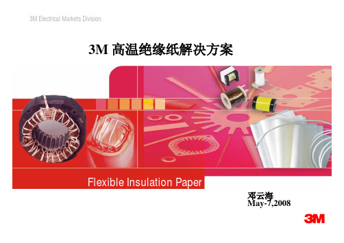
3M 高温绝缘纸解决方案邓云海May-7,20082Copyright ©3M 2008. 3M External Release3M高温绝缘纸解决方案IPT: Innovative Paper Technologies n 原产地美国n 无机成分为主n 耐高温等级H 级以上,180o C~220oC3Copyright ©3M 2008. 3M External Release3M 高温绝缘纸简介4Copyright©3M 2008. 3M External Release电机、发电机中的应用玻璃布胶带5Copyright ©3M 2008. 3M External Release槽楔绝缘: TufQUIN TFT DMD180交流发电机定子Class 155℃& 180℃电机、发电机中的应用CeQUIN B-stage半固化树脂预浸牵引电机6Copyright ©3M 2008. 3M External Release按冷却方式分:n 干式变压器:绝缘介质是树脂或纸和绝缘漆,冷却方式有自冷和风冷,优点是免维护>通风型干式变压器(OVDT Open Ventilated Dry-Type)大量采用绝缘纸作为绝缘介质> 树脂浇注式干变n 油浸式变压器:绕组浸在变压器油中,油作绝缘和冷却介质变压器的类型7Copyright ©3M 2008. 3M External Release绝缘纸用于导线绕包-匝绝缘干式变压器中的绕线应用VPI真空压力浸漆浸漆后浸漆工艺作用:ü提高整体性ü降低运行温度和温升ü提高可靠性,抗污抗潮3M 绝缘纸优异的吸漆性能,有利于变压器稳定可靠的工作!8Copyright ©3M 2008. 3M External ReleaseStrip Coil Transformers箔绕式变压器绝缘纸层间绝缘箔绕变压器中的绝缘纸应用•端部绝缘•层间绝缘•对地绝缘铜箔/铝箔9Copyright ©3M 2008. 3MExternal Release微波炉用变压器UPS 电源变压器焊接机用的变压器高温绝缘纸的应用特种变压器HID 照明镇流器10Copyright ©3M 2008. 3M External Release柔软强韧抗溶剂/化学品高绝缘性能500 V/mil bdV高无机含量高耐温性柔软强韧阻燃TuFR UL94-V0等级特性聚合物为主无机物为主主成分220o C Class (R)220o C Class (R)220o C Class (R)200o C Class (N)UL 1446 绝缘系统认证ThermalShield ™ThermaVolt ™CeQUIN ®TufQUIN ®3M 高温绝缘纸产品系列* 典型厚度范围0.05mm~1.5mm ,CeQUINBORD 0.8mm~6.4mm11Copyright ©3M 2008. 3M External Release覆合结构:•覆合不同类型/厚度的薄膜例:TFT 3-5-3: 3mil TufQUIN + 5mil Film + 3mil TufQUINIF 5-2: CeQUN 5mil + Film 2mil3M 高温绝缘纸复合产品系列12Copyright ©3M 2008. 3M External Release绝缘纸作为绝缘材料的首要作用:在电气设备中把电势不同的带电部分隔离开来应用中对绝缘纸的特性要求n 较高的绝缘耐压强度,以避免发生漏电、击穿等事故n 高耐热性能,避免因长期过热而老化变质n 良好的导热性、耐潮性n 较高的机械强度,工艺加工方便通常高温绝缘纸的特性要求13Copyright ©3M 2008. 3M External Release特性好处1. 吸湿率低减少烘干工艺,降低使用成本;尺寸稳定,可靠性好2. 导热性好有利于散热,设备运行时温度更低,寿命更长3. 绝缘漆浸润效果好线圈更紧密,减少工作时噪音,有利散热4. 高温下长期耐电压设备发热和过负载工作时的可靠性3M 高温绝缘纸特性14Copyright ©3M 2008. 3M External ReleaseTufQUIN 高温老化后的耐压测试,240o C, 2130hrs高低温冲击长期耐压3M 绝缘纸可靠性测试15Copyright ©3M 2008. 3M External Releaseü全面的UL 绝缘系统认证ü多种绝缘漆ü3M 电气胶带包括在内绝缘系统列表,UL 档案号E65007绝缘系统-180o C ~220o C 温度等级UL 绝缘系统认证16Copyright ©3M 2008. 3M External Release绝缘纸选型17Copyright ©3M 2008. 3M External ReleaseQ & A。

A V R单片机相关问题AVR单片机相关问题AVR读写外部RAM时出现的问题问:1,对AT90S8515来说,外部RAM的地址肯定是从0x0260开始的?2,我用ICE200仿真8515读写外部RAM,RAM大小为32K Bytes,地址映射到0x0000-0x7fff,用PC7做它的片选。
把SRE置为1,当我访问0x0300时PC7为低,这是对的,但当我不去访问0x0000-0x7fff地址空间时(例如进入死循环),问题出现了,此时PC7仍为低,按道理应为高的。
这是阿AVR与51的不同,还是我弄错了。
答:1、对AT90S8515来说,外部RAM的地址肯定是从0x0260开始的。
这是没问题的,访问0x0000-0x025F的地址为内部RAM。
2、当你访问过0x0300,PC7为低,当你不访问0x0000-0x7FFF时,由于没有一条把PC7置高的指令,所以PC7当然还为低了。
不过这也不要紧,因为当你访问0x0000-0x025F的时候,RD和WR是没有的,所以即使外部RAM被选中了,没不会产生读写。
当你访问0x0260-0x7FFF的时候,RD和WR就自动产生了。
所以就是你把外部RAM的CS直接接地也是可以的。
Mon,26 Mar 2007 15:45:57 GMT以前看到#define SREG(*(volatile unsigned char*)0x5F)这样的定义,总是感觉很奇怪,不知道为什么,今天终于有了一点点心得,请大虾们多多批砖~嵌入式系统编程,要求程序员能够利用C语言访问固定的内存地址。
既然是个地址,那么按照C语言的语法规则,这个表示地址的量应该是指针类型。
所以,知道要访问的内存地址后,比如0x5F,第一步是要把它强制转换为指针类型(unsigned char*)0x5F,AVR的SREG是八位寄存器,所以0x5F强制转换为指向unsigned char类型。
volatile(可变的)这个关键字说明这变量可能会被意想不到地改变,这样编译器就不会去假设这个变量的值了。


510(k) SUBSTANTIAL EQUIVALENCE DETERMINATIONDECISION SUMMARYINSTRUMENT ONLY TEMPLATEA. 510(k) Number:k170983B.Purpose for Submission:Modification of a previously cleared device to add a 6 second exhalation modeC.Manufacturer and Instrument Name:Circassia AB NIOX VEROD.Type of Test or Tests Performed:QuantitativeE. System Descriptions:1. Device Description:NIOX VERO is a portable system for the non‐invasive, quantitative measurement of the fraction of exhaled nitric oxide (NO) in expired human breath (FeNO).The NIOX VERO system is comprised of the NIOX VERO unit with AC adapter, arechargeable battery, an electrochemical NO sensor, disposable patient filters, and anexchangeable handle containing an internal NO scrubber filter. The NIOX Panel is anoptional PC application for operation of the NIOX VERO from a PC and access toelectronic medical record systems. The device can connect to the PC via a standard USB cable or wirelessly via Bluetooth.For testing, the patient empties their lungs, inhales deeply through the patient filter tototal lung capacity and then slowly exhales for 6 or 10 seconds, depending on the mode of operation. The default mode of operation is the 10 second exhalation mode. Inapproximately one minute, the NO concentration is displayed in parts per billion (ppb).Results are processed using dedicated software. The device has built‐in system controlprocedures and a Quality Control procedure to be performed on a daily basis.2. Principles of Operation:The measurement principle is based on American Thoracic Society guidelines (ATS/ERS Recommendations for Standardized Procedures for the Online and Offline Measurement of Exhaled Lower Respiratory Nitric Oxide and Nasal Nitric Oxide, 2005. Am J RespirCrit Care Med. 2005;171:912-930). The last three second fraction of a 6 second or 10 second exhalation is evaluated for average NO concentration. The exhalation flow is controlled to 50 ml/s ±5 ml/s at an applied pressure of 10 to 20 cm H2O. Sample isevaluated in 25 seconds (2 ml/sec for 25 seconds). The inhaled air is NO free. NO is measured using electrochemical detection. There is a gas inlet chamber with anelectrolyte (sulfuric acid solution) and hardware. The NO molecules diffuse through the membrane and reach the electrolyte. A chemical reaction takes place where one electron for each NO molecule is generated. The current is proportional to the number ofconverted NO molecules.3. Modes of Operation:Does the applicant’s device contain the ability to transmit data to a computer, webserver, or mobile device?Yes ___X____ or No ________Does the applicant’s device transmit data to a computer, webserver, or mobile device using wireless transmission?Yes ___X____ or No ________4. Specimen Identification:There is no mechanism to identify the specimen.5. Specimen Sampling and Handling:The user obtains a breath sample by exhaling into the device.6. Calibration:The manufacturer performs calibration for each NIOX VERO sensor. NIOX VERO sensor is an electrochemical sensor pre-calibrated and pre-programmed for a defined number of tests (60, 100, 300, 500, or 1000 tests).The user exchanges the sensor upon expiration. The instrument prompts the user for upcoming exchange prior to sensorexpiration and does not allow for measurements with an expired sensor. No additional calibration is needed during the lifetime of the sensor.7. Quality Control:NIOX VERO provides internal controls as well as an External Quality Control program for the user to verify the reliability of measurements.8. Software:FDA has reviewed applicant’s Hazard Analysis and Software Development processes for this line of product types:Yes___X____ or No________F. Regulatory Information:1. Regulation section:21 CFR 862.3080, Breath nitric oxide test system2. Classification:Class II3 Product code:MXA4. Panel:Clinical Chemistry (75)G. Intended Use:1. Indication(s) for Use:NIOX VERO measures Nitric Oxide (NO) in human breath. Nitric Oxide is frequentlyincreased in some airway inflammatory processes such as asthma. The fractional NOconcentration in expired breath (FeNO), can be measured by NIOX VERO according to guidelines for NO measurement established by the American Thoracic Society.Measurement of FeNO by NIOX VERO is a quantitative, non-invasive, simple and safe method to measure the decrease in FeNO concentration in asthma patients that oftenoccurs after treatment with anti-inflammatory pharmacological therapy, as an indication of the therapeutic effect in patients with elevated FeNO levels. NIOX VERO is suitable for children, 7- 17 years, and adults 18 years and older.NIOX VERO 10 second test mode is for age 7 and up.NIOX VERO 6 second test mode is for ages 7-10 only who cannot successfully completea 10 second test.FeNO measurements provide the physician with means of evaluating an asthma patient'sresponse to anti-inflammatory therapy, as an adjunct to the established clinical andlaboratory assessments in asthma. The NIOX VERO is intended for prescription use and should only be used as directed in the NIOX VERO User Manual by trained healthcareprofessionals. NIOX VERO cannot be used with infants or by children under the age of 7 as measurement requires patient cooperation.NIOX VERO should not be used in critical care, emergency care or in anesthesiology.2. Special Conditions for Use Statement(s):NIOX VERO should only be operated by trained healthcare professionals and only after careful reading of the NIOX VERO User Manual.The device should not be used with infants or by children under the age of 7, or anypatient who cannot cooperate with any necessary requirements of test performance.The device should not be used in critical care, emergency care or in anaesthesiology.Subjects should not smoke in the hour before measurements, and short- and long-termactive and passive smoking history should be recorded. In addition, subjects shouldrefrain from eating and drinking for 1 hour before exhaled NO measurement. Alcoholingestion reduces FENO in patients with asthma and healthy subjects FENO.It is prudent, where possible, to perform serial NO measurements in the same period ofthe day and to always record the time.For prescription use only.H. Substantial Equivalence Information:1. Predicate Device Name(s) and 510(k) numbers:NIOX VERO Airway Inflammation Monitor; k1502332. Comparison with Predicate Device:I. Special Control/Guidance Document Referenced (if applicable):·AAMI/ANSI ES60601-1:2005/(R)2012 And A1:2012,C1:2009/(R)2012 And A2:2010/(R)2012(Consolidated Text) Medical·IEC 60601-1-6 Edition 3.1 2013-10, Medical Electrical Equipment - Part 1-6: General Requirements For Basic Safety And Essential·AAMI / ANSI / ISO 14971:2007/(R)2010, Medical Devices - Applications Of Risk Management To Medical Devices·CLSI EP5-A2 Vol 24 No. 25 Evaluation of Precision Performance of Quantitative Measurement methods·CLSI EP6-A vol 23, no. 16, Evaluation of the Linearity of Quantitative Measurement Procedures: A Statistical Approach·CLSI EP09-A2, Measurement Procedure Comparison And Bias Estimation Using Patient Samples; Approved Guideline – Third Edition. (InVitro Diagnostics) ·CLSI EP09-A3, Measurement Procedure Comparison And Bias Estimation Using Patient Samples; Approved Guideline – Third Edition. (InVitro Diagnostics)J. Performance Characteristics:1. Analytical Performance:a. Accuracy:A method comparison study was performed to assess the agreement between the 6second and 10 second exhalation modes of the NIOX VERO in patients ages 7 – 10.The difference in FeNO measurements between the 6 second and 10 secondexhalation modes was not clinically significant.b. Precision/Reproducibility:Analytical precision for the 6 second exhalation mode was evaluated based on theCLSI standard EP5-A2. A certified NO calibration gas concentration of 200 ppb wasmixed with nitrogen gas in a gas mixer to create concentrations of 5, 25, 75, and 200ppb. Data was collected over 20 operating days, two runs per day, with duplicatedeterminations for each concentration. The repeatability and within-device precisionover 20 days were determined for each concentration. Five NIOX VERO sensors,continually mounted in 5 NIOX VERO instruments, respectively, were used. Theresults at the 5 and 25 ppb levels, expressed as standard deviation (ppb), and at the 75and 200 ppb levels, expressed as percent CV (%), are as follows:c. Linearity:Linearity of measurements using the 6 second exhalation mode was determined using certified NO at 200 ppb and 2000 ppb in nitrogen calibration gas mixed with nitrogen gas in a gas mixer, connected in-line with the NIOX VERO instrument, (withmounted NIOX VERO sensors), to obtain 7 NO concentration levels (3, 5, 25, 100,200, 300 and 330 ppb). Five replicate determinations of the concentrations at 3 and 5 ppb, and three replicate determinations on the other intervals were made.For the 10 devices tested, the regression analysis gave slopes of 1.05 to 1.09 andintercept ± 4 ppb. The squared correlation coefficient r2 was 0.999 for all 10 devices tested. Results indicate linearity within the 5-300 ppb measuring range.Effects of Temperature and Relative HumidityThe effects of temperature and relative humidity were characterized in k133898.Please refer to the Decision Memorandum for k133898 for details.d. Carryover:Not applicablee. Interfering Substances:The effect of potentially interfering substances was characterized in k133898.2. Other Supportive Instrument Performance Data Not Covered Above:Other clinical supportive data:A clinical study was not conducted with the 6 second mode of the NIOX VERO device.In 2007, a multi-center device randomized open-label prospective single-cohort study was conducted to demonstrate substantial equivalence between NIOX MINO andpredicate device (NIOX) when measuring the change of FeNO that often occurs after 2 weeks of corticosteroid therapy compared to their baseline levels. Symptomatic asthmatic males and females performed two valid FeNO measurements at each visit, with NIOX MINO and NIOX respectively, with a limit of six exhalation attempts per subject in each device. The order of the FENO measurement on NIOX MINO versus NIOX wasrandomized. At every visit and for every patient, spirometry was performed and asthma symptoms were recorded using Asthma Control Questionnaire (ACQ). In total, 156subjects were included, 105 adults 18 - 70 years old and 51 children 7 - 17 years old.Results from this study, in conjunction with the new method comparison study described above, were determined to be applicable to the 6 second mode of the candidate device, the NIOX VERO. See k072816 for more details.Traceability, Stability, Expected values (controls, calibrators, or methods):The NIOX VERO instrument is calibrated by the manufacturer and does not requirecalibration by the user. A replaceable sensor is used which is pre-programmed and pre-calibrated for a defined number of tests. The life time of NIOX VERO instrument is setto 5.5 years. The number of possible tests is 15000. The sensor life time is limited to 12 months in unopened packaging following manufacture, for 6 months from initialinstallation into NIOX VERO, or for the defined number of tests (60, 100, 300, 500 or1000), whichever comes first. The shelf life for NIOX Filter in unopened primarypackage is 2 years. NIOX Filter is for single use and must be replaced for every newpatient and measurement occasion. Stability information to support all claims wasreviewed in k133898.Detection limit:The detection limit of the NIOX VERO using the 6 second mode was determined in alaboratory setting, using mixtures of standard reference NO gas and nitrogen gas belowand above the detection limit, at 3 and 5 ppb. Five replicate determinations of eachconcentration were made. 10 NIOX VERO sensors, continually mounted in 10 NIOXVERO instruments, respectively, were used in these tests. The results of the study support the claimed detection limit of 5 ppb for the 6 second mode.Expected values/Reference range:The expected values are provided from the literature. In the labeling the sponsor states,“Given that physiological and environmental factors can affect FeNO, FeNO levels inclinical practice need to be established on an individual basis. However, most healthyindividuals will have NO levels in the range 5-35 ppb (children slightly lower, 5-25 ppb) when measured at 50 ml/s.(ATS/ERS Recommendations for Standardized Procedures for the Online and OfflineMeasurement of Exhaled Lower Respiratory Nitric Oxide and Nasal Nitric Oxide, 2005.Am J Respir Crit Care Med. 2005;171:912-930.)”K. Proposed Labeling:The labeling is sufficient and it satisfies the requirements of 21 CFR Part 809.10.L. Conclusion:The submitted information in this premarket notification is complete and supports asubstantial equivalence decision.。
for external use only的意思**"For External Use Only"的含义解析**在日常生活中的各种产品包装上,我们经常可以看到“For External Use Only”的标识。
这句话究竟是什么意思?它对消费者使用产品又有何影响?以下,我们将详细解析这一短语的含义及其背后的重要性。
“For External Use Only”直译为“仅供外用”,这是产品制造商在使用说明中常用的一句话,意在提醒和指导消费者,该产品仅适用于外部使用,不得内服或用于身体内部。
这种标识通常出现在药品、化妆品、清洁剂等产品的包装上。
**具体含义:**1.**使用范围的限定:** 当产品标有“仅供外用”时,表明产品仅设计用于皮肤表面或物体外部的清洁、治疗、保养等,不得用于眼睛、口腔、鼻腔、阴道或直肠等身体内部。
2.**安全警示:** 这句话也是一种安全警示,提示消费者若误用或不当使用该产品,可能会导致健康风险或产品效果不佳。
3.**成分说明:** 许多外用产品含有不适合内服的成分,比如某些刺激性化学物质,这些成分可能对身体内部造成伤害。
**为何重要?**- **保障消费者健康:** 正确理解和使用“仅供外用”标识,可以避免因误用导致的健康问题。
- **确保产品效果:** 每种产品都是根据其使用部位和作用机理设计的,正确使用才能发挥其预期效果。
- **法律责任:** 制造商在产品上贴上此类标签,也是为了遵守相关法律法规,保护自身免受因消费者误用而产生的法律责任。
**总结:**消费者在购买和使用产品时,应仔细阅读产品标签,注意“For External Use Only”等使用指示。
正确理解和使用产品,不仅能够保障个人健康,还能使产品发挥最大的效果。
ELC-PV28NNDR ELC-PV28NNDTELC that is micro, multi-functional, and with various instructionsInstruction SheetWARNINGThis instruction sheet only provides introductory information on electrical specification, functions, trouble-shooting and peripherals. For more information, please refer to “ELC System Manual ”.∙ This is an OPEN TYPE Controller. The ELC should be kept in an enclosure away from airborne dust, humidity, electric shock risk and vibration. Also, it is equipped with protective methods such as some special tools or keys to open the enclosure, so as to avoid the hazard to users and the damage to the ELC.∙ Never connect the AC main circuit power supply to any of the input/output terminals, as it will damage the ELC. Check all the wiring prior to power up. To avoid any electromagnetic noise, make sure the ELC is properly grounded. DO NOT touch terminals when power on.∙ Power, input and output (I/O) wiring must be in accordance with Class І, Division 2 wiring methods – Article 501-10(B)(1) of the National Electrical Code.∙ Suitable for use in Class І, Division 2, Groups A, B, C, D or non-hazardous locations only. ∙ Explosion hazard - Substitution of components may impair suitability for Class І, Division 2.∙ Explosion hazard - DO NOT disconnect equipment unless power has been switched off or the area is known to be non hazardous. ∙ Ambient temperature 55°C.∙Operating Temperature Code T4A.1INTRODUCTION1.1 Model Name Explanation & PeripheralsThank you for choosing Eaton Logic Controller (ELC) series products. The ELC-PV series are 28-point (16 inputs + 12 outputs) controllers offering various instructions and 16K Steps program memory to connect with ELC series extension models which includes digital input/ output (max. 512 input/ output extension points), analog modules (A/D, D/A transformation and temperature units) and all kinds of new high-speed extension modules. Its 4-grouphigh-speed (200KHz) pulse outputs and the two new 2-axis interpolation instructions satisfy all kinds of applications. ELC-PV is small in size and easy to install.1.2 Product Profile & Outline12345671410981312117039031718161560201921Unit: mm1 Status indicators of POWER, RUN, BAT.LOW and ERROR2 COM1(RS-232) (Rx) indicator3 COM2(RS-485) (Tx) indicator4 I/O point indicators5 RUN/STOP switch6 VR0: Start-up by M1178/D1178 corresponding value7 VR1: Start-up by M1179/D1179 corresponding value 8 I/O terminal 9 COM1(RS-232) port10 DIN rail clip11 Extension module positioning hole12 Extension port for wire to connect extension module/unit 13 DIN rail track (35mm) 14 Extension unit clip15 RS-485 communication port (Master/Slave) 16 DC Power input17 3 pin removable terminal (standard component) 18 Power input cable (standard accessory)19 New high-speed extension module connection port 20 Nameplate21 Direct fastening hole2SPECIFICATIONSItemSpecificationNoteOperation control method Stored program; cyclic scanning systemI/O control methodBatch processing and refresh I/O status when END instruction is executed With instruction that can immediately refresh I/O status Operation processing speed Basic instruction (min. 0.24 us) Application instruction Program language Instruction + ladder diagram + SFC With step instructionProgram capacity 15,872 STEPSSRAM + rechargeable battery + Flash Instruction type32 basic sequential instructions (including step ladder instructions)193 application instructionsItemSpecificationNoteR e l a y (b i t )X External input relay X0 ~ X377, octal encoding; 256 points Total512 points Corresponds to external input pointsYExternal output relayY0 ~ Y377, octal encoding; 256 points Corresponds to external output pointsMAuxiliary relayGeneral purposeM0 ~ M499, 500 points (*2) Total4,096pointsThe contact can be On/Off in theprogram.Latched M500 ~ M999, 500 points (*3) M2000 ~ M4095, 2,096 points (*3) Special purposeM1000 ~ M1999, 1,000 points (part for latched)T Timer100 msT0 ~ T199, 200 points (*2) Total 256 points Timer indicated by TMR instruction. If timing reaches its target, the T contact of the same No. will be On.T192 ~ T199 for subroutineT250 ~ T255, 6 accumulative points (*4) 10 ms T200 ~ T239, 40 points (*2)T240 ~ T245, 6 accumulative points (*4) 1 ms T246 ~ T249, 4 accumulative points (*4) C Counter16-bitcounting up C0 ~ C99, 100 points (*2) Total253pointsCounter indicated by CNT (DCNT)instruction. If counting reaches itstarget, the C contact of the sameNo. will be On.C100 ~ C199, 100 points (*3) 32-bit counting up/downC200 ~ C219, 20 points (*2) C220 ~ C234, 15 points (*3)32-bit high-speedcounting up/downC235 ~ C244, 1 phase 1 input, 10 points (*3)C246 ~ C249, 1 phase 2 inputs, 4 points (*3)C251 ~ C254, 2 phase 2 inputs, 4 points (*3)S Step points InitialS0 ~ S9, 10 points (*2)Total 1,024 pointsUsed for SFCLatched area setup Start: D1214(K500) End: D1215(K899)For zero returnS10 ~ S19, 10 points, used with IST instruction (*2)General purposeS20 ~ S499, 480 points (*2) Latched S500 ~ S899, 400 points (*3) For alarmS900 ~ S1023, 124 points (*3) R e g i s t e r (w o r d d a t a )T Present value in timer T0 ~ T255, 256 pointsWhen timing reaches the target, the contact continuity of timer appears. CPresent value in counterC0 ~ C199, 16-bit counter, 200 pointsWhen counting reaches the target, the contact continuity of counter appears.C200 ~ C254, 32-bit counter, 53 points DData registerGeneral purposeD0 ~ D199, 200 points (*2) Total 10,000 points Memory area for data storage; can be used for special indirect indication.Latched D200 ~ D999, 800 points (*3) D2000 ~ D9999, 8,000 points (*3) Special purpose D1000 ~ D1999, 1,000 points For Indirect indicationE0 ~ E7, F0 ~ F7, 16 points (*1) N/A File register0 ~ 9,999 (10,000 points) (*4) Extension register for data storage I n d e xN For main control loop N0 ~ N7, 8 points Control point for main control loop PFor CJ, CALL instructions P0 ~ P255, 256 pointsPosition index of CJ and CALLII n t e r r u p t i o n s u b r o u t i n eExternal interruptionI0000/I0001(X0), I1000/I1001(X1), I2000/I2001(X2), I3000/I3001(X3), I4000/I4001(X4), I5000/I5001(X5),6 points (01: rising-edge trigger; 00: falling-edge trigger)Position index for interruption subroutineTime interruption I601~I699 (1ms), I701~I799 (1ms), I801~I899 (0.1ms) Interruption when high-speed counting reaches its target I010, I020, I030, I040, I050, I060, 6 points Interruption during pulse outputI110, I120, I130, I140, 4 points Interruption during communicationI150, I160, I170, 3 pointsC o n s t a n tK Decimal K-32,768 ~ K32,767 (16-bit operation)K-2,147,483,648 ~ K2,147,483,647(32-bit operation )H HexH0000 ~ HFFFF (16-bit operation), H00000000 ~ HFFFFFFFF (32-bit operation) FFloating pointDisplaying floating points by the length of 32 bits with IEEE754 standard ±1.1755 × 10-38 ~ ±3.4028 × 10+38Serial communication ports (program write in/read out) COM1: RS-232; COM2: RS-485 (can be master or slave); COM1 and COM2 can be used at the same time Potentiometer / RTC Built-in 2 points VR / Built-in RTCSpecial extension moduleRight-side extension module and PB series share all modules (max. 8 modules extendable) Left-side can be connected with new high-speed extension modules (max. 8 module extendable)*1: Non-latched area cannot be modified.*2: The preset non-latched area can be modified into latched area by setting up parameters. *3: The preset latched area can be modified into non-latched area by setting up parameters. *4: The fixed latched area cannot be modified.After the 24V DC power is switched off, the data in the latched area is stored in SRAM memory which is powered by the rechargeable battery. When the battery is damaged or cannot be changed, the data in the program and latched area will be lost. If the user needs to permanently save the data in the latched area in the program and device D, please refer to “Flash ROM permanently saved and recover mechanism ” as stated below. Permanently saved mechanism:The user can use ELCSoft (Options -> ELC<=>Flash) to indicate whether to permanently store the data in the latched area in the program (including password) and device D in Flash ROM memory (new indicated data will replace all data previously saved in the memory). Recover mechanism:If the rechargeable battery is in low voltage, resulting in the loss of data in the program, ELC will automatically restore the data in the latched area in the program and device D of Flash ROM into SRAM memory (M1176 = On) next time when 24V DC is re-powered. The ERROR LED flashing will remind the user that if the recorded program is able to resume its execution, the user only needs to shut down and re-power the ELC once to restart its operation (RUN).3ELECTRICAL SPECIFICATIONSModel ItemELC-PV28NNDRELC-PV28NNDTPower supply voltage24VDC (-15% ~ 20%) (with counter-connection protection on the polarity of DC input power) Inrush current Max. 2.2A@24VDC Power consumption 6WInsulation resistance>5 M Ω (all I/O point-to-ground: 500VDC)Noise immunityESD (IEC 61131-2, IEC 61000-4-2): 8KV Air DischargeEFT (IEC 61131-2, IEC 61000-4-4): Power Line: 2KV; Digital I/O: 1KV, Analog & Communication I/O: 1KVDamped-Oscillatory Wave: Power Line: 1KV, Digital I/O: 1KV RS (IEC 61131-2, IEC 61000-4-3): 26MHz ~ 1GHz, 10V/mEarthThe diameter of grounding wire shall not be less than that of the wiring terminal of the power. (When many PLCs are in use at the same time, please make sure every PLC is properly grounded.)Operation/storageOperation: 0ºC ~ 55ºC (temperature); 50 ~ 95% (humidity); pollution degree 2 Storage: -25ºC ~ 70ºC (temperature); 5 ~ 95% (humidity)Vibration/shock immunity International standards: IEC61131-2, IEC 68-2-6 (TEST Fc)/IEC61131-2 & IEC 68-2-27 (TEST Ea) Certificates CE, ULWeight (g)260g240gInput pointType Current Motion levelResponding time DC (Sink or Source)24VDC 5mAX0~X7,X12~X13,X16~X17Off ✂On >16.5VDCX10~X11,X14~X15Off ✂On >18.5VDC X0~X17 On ✂Off <8VDCApprox. 10 ms (can be adjusted within the range of 10 ~ 60 ms by D1020 and D1021)Output pointTypeCurrentVoltageMax. loadingRespondingtimeMechani-cal life Electrical life relay-R1.5A/1 point (5A/COM) 250VAC, >30VDC75VA (inductive) 90 W (resistive) Approx. 10 ms2×107times (without load)1.5×105 times (5A 30VDC) 5×105 times (3A 120VAC)3×104 times (5A 250VAC)transistor-TGeneral: 0.3A/1 point @40ºCHigh-speed: <1kHz, 0.3A/1 point @ 40ºC; ≥ 1kHz,30mA/1point@40 ºC30VDCMax. 10kHz for Y5, Y7, Y10 ~ Y13 Off ✂On 20us On ✂Off 30us--Max. 200kHz for Y0, Y1, Y2, Y3, Y4, Y6Off ✂On 0.2us On ✂Off 0.2us4MODEL NAME & I/O CONFIGURATIONModelInput/output specificationI/O configuration PowerInputOutputRelayTransistorPointTypePointTypeELC-PV28NNDR24VDC 16 DC (Sink Or Source12RelayS S X 0X 1X 2X 3X 4X 5X 6X 7S S X 10X 11X 12X 13X 15X 16X 17C 0Y 0Y 1Y 2Y 3Y 4Y 5Y 6Y 7Y 10Y 11Y 12Y 13C 1C 2C 3S S X 0X 1X 2X 3X 4X 5X 6X 7S S X 10X 11X 12X 13X 15X 16X 17C 0Y 0Y 1C 1C 2Y 4Y 5Y 6Y 7Y 12Y 13C 3Y 2Y 3C 4Y 10Y 11ELC-PV28NNDT Transistor5INSTALLATION & WIRING5.1 Mounting & WiringThe ELC can be secured to a cabinet by using the DIN rail of 35mm in height and 7.5mm in depth. When mounting ELC to DIN rail, be sure to use the end bracket to stop any side-to-side movement of ELC and reduce the chance of wires being loose. A small retaining clip is at the bottom of ELC. To secure ELC to DIN rail, place the clip onto the rail and gently push it up. To remove it, pull the retaining clip down and gently remove ELC from DIN rail, as shown in figure 1.Please use M4 screw (see figure 2) according to the dimension of the product. Please install ELC in an enclosure with sufficient space around it to allow heat dissipation (see figure 3).9053.270101109.4PLC DDDDD > 50 mmFigure 1Figure 2 (Unit: mm)Figure 35.2 Wiring1. Use 22-16AWG (1.5mm) single or multiple core wire on I/O wiring terminals. Thespecification of the terminal is shown in the figure on the left. The ELC terminalscrews shall be tightened to 1.95 kg-cm (1.7 in-lbs).2. DO NOT place the I/O signal wires and power supply wire in the same wiring duct.3. Use 60/75 ºC copper wires only.DO NOT install ELC in an environment with:1. Dust, smoke, metallic debris, corrosive or flammable gas2. High temperature, humidity3. Direct shock and vibration5.3 Power Input WiringThe power input of ELC-PV series is DC. When operating ELC-PV series, please make sure that:1. The power is connected to the two terminals, 24VDC and 0V, and the range of power is 20.4VDC ~28.8VDC. If the power voltage is less than 20.4VDC, ELC will stop running, all outputs will go “Off” andERROR indicator will flash continuously.2. A power shutdown of less than 10 ms will not affect the operation of ELC. However, power shutdown timethat is too long or a drop of power voltage will stop the operation of ELC and all outputs will go “Off”. Whenthe power supplied again, ELC will automatically return to its operation. (Please be aware of the latchedauxiliary relays and registers inside ELC when programming.)DC power input5.4 Input point wiringThere are two types of DC inputs, SINK and SOURCE.5.5 Output point wiring5.6 Relay (R) contact circuit wiring5.7 Transistor (T) contact circuit wiring■Preparation1. Prior to applying power, please verify that the power lines and the input/output wiring are correct. And beadvised not to supply 110V AC or 220V AC into the I/O terminals, or it might short-circuit the wiring andwould cause direct damage to the ELC.2. After using the peripheral devices to write the program into the ELC and that the ERROR LED of the ELCis not on, it means that the program in use is legitimate, and it is now waiting for the user to give the RUNcommand.3. Use ELC-HHP to execute the forced On/Off test of the output contact.■Operation & test1. If the ERROR indicator does not flash, you can use the RUN/STOP switch or a peripheral device(ELC-HHP or ELCSoft) to give a RUN instruction. The RUN indicator should be continuously on at thistime. That the RUN indicator does not flash indicates ELC has no program in it.2. When ELC is in operation, use ELC-HHP or ELCSoft to monitor the set value or temporarily saved valuein timer (T), counter (C), and register (D) and force On/Off of output contacts. That the ERROR indicatoris on (not flashes) indicates that part of the program exceeds the preset time-out. In this case, you have toset the RUN/STOP switch as STOP first, check special register D1008 and obtain the location in theprogram where time-out takes place. Please refer to the WDT instruction to solve this problem.■Operation of ELC basic sequential instructions & application instructions1. The basic sequential instructions and application instructions of ELC-PV series are compatible with allELC series ELCs. See Eaton “ELC System Manual” for relevant information.2. All ELC series ELCs are compatible with ELC-HHP handheld programming panel, ELCSoft ladderdiagram for program editing and exclusive transmission cables to connect with ELC-PV for programtransmission, ELC control, program monitoring and so on.Based on the indicators on the front panel, please check the following for errors:☼POWER indicatorWhen ELC is powered, the POWER LED indicator on the front panel will be on (in green). If this indicator is noton or the ERROR indicator keeps flashing when ELC is powered indicates that the power supply +24V areinsufficient or DC power supply 24V is overloaded. In this case, change another 24V DC power supply. If theindicator is still off at this time, your ELC is malfunctioned. Send your ELC back to your distributor for repair.☼RUN indicatorCheck your ELC status. When ELC is running, this indicator will be on. You can use ELC-HHP, the ladderdiagram editing program or the switch on the panel to RUN or STOP ELC.☼ERROR indicatorIf you enter illegal program into ELC or use instructions or devices that exceed their range, this indicator willflash (approx. every 1 second). When this happens, you have to obtain the error code from D1004 and save theaddress where the error occurs in register D1137 (if the error is a general circuit error, the address of D1137 willbe invalid). Find out the cause of the error, amend the program and resend the program to ELC. If you cannotconnect to ELC and this indicator keeps flashing quickly (approx. every 0.2 second), it means that the 24VDCpower voltage is insufficient. Please check if the 24V DC is overloaded.If the ERROR indicator is on, you have to check the special relay M1008. If M1008 is on indicates that theexecution time of program loop exceeds the preset time-out (in D1000). In this case, turn the RUN/STOP switchto STOP, check the special register D1008 and obtain the location in the program where the time-out takesplace. Please refer to the WDT instruction to solve this problem. After amending the program, you only need toresend the program to stop the indicator from flashing. If the indicator still keeps flashing at this time, switch offthe power and check if there is any interference existing or conductive matter inside ELC.For details of error codes (in D1004, hex coding), see “ELC System Ma nual: Programming”.☼BAT.LOW indicatorThe rechargeable lithium-ion battery in ELC-PV is mainly used on the latched procedure and data storage.The lithium-ion battery has been fully charged in the factory and is able to retain the latched procedure and datastorage for 12 months. If ELC-PV has not been powered and used for more than 12 months, the battery will beout of power upon normal consumption and the procedure and data will be lost.The lithium-ion battery has longer life span than ordinary battery; therefore there is no need to change batteryvery frequently. You can charge the battery at any time without having to worry about a decrease in chargeability.You can also recharge the battery even when there is still power in the battery.Please be aware of the date of manufacturing; the charged battery can sustain for 12 months from this date. Ifyou find that the BAT.LOW indicator stays on after ELC is powered, the battery voltage is low and the battery isbeing charged. ELC-PV has to remain on for more than 24 hours to fully charge the battery. If the indicator turnsfrom on to “flash” (every 1 second), it indicates that the battery cannot be charged anymore. Please correctlyprocess your data in time and send the ELC back to Eaton for changing a new battery.Precision of calendar timer:At 0°C/32°F, less than –117 seconds error per month.At 25°C/77°F, less than 52 seconds error per month.At 55°C/131°F, less than –132 seconds error per month.☼Input indicatorOn/Off of input point is indicated by input indicator or monitored by ELC-HHP. When the action condition of theinput point is true, this indicator will be on. If abnormality is identified, check if the indicator and input circuit arenormal. Use of electronic switch with too much electricity leakage often results in unexpected actions of theinput point.☼Output indicatorOn/Off of output point is indicated by the output indicator. When the output indicator (On/Off) does notcorrespond to the action of its load, please be aware of the following:1. The output contact may be melted or blocked due to an over loaded or short-circuited load, which will resultin poor contact.2. If you are suspicious that the output point may execute an undesired action, check the output wiring circuitand whether the screw is properly tightened.。
STM32F429xx ARM Cortex-M432b MCU+FPU,225DMIPS,up to2MB Flash/256+4KB RAM,USBOTG HS/FS,Ethernet,17TIMs,3ADCs,20comm.interfaces,camera&LCD-TFTData brief Features•Core:ARM32-bit Cortex™-M4CPU with FPU,Adaptive real-time accelerator(ARTAccelerator™)allowing0-wait state executionfrom Flash memory,frequency up to180MHz, MPU,225DMIPS/1.25DMIPS/MHz(Dhrystone2.1),and DSP instructions •Memories–Up to2MB of Flash memory organized into two banks allowing read-while-write –Up to256+4KB of SRAM including64-KB of CCM(core coupled memory)data RAM –Flexible external memory controller with up to32-bit data bus:SRAM,PSRAM,SDRAM,Compact Flash/NOR/NAND memories •LCD parallel interface,8080/6800modes •LCD-TFT controller up to VGA resolution with dedicated Chrom-ART Accelerator™forenhanced graphic content creation(DMA2D)•Clock,reset and supply management– 1.8V to3.6V application supply and I/Os–POR,PDR,PVD and BOR–4-to-26MHz crystal oscillator–Internal16MHz factory-trimmed RC(1% accuracy)–32kHz oscillator for RTC with calibration–Internal32kHz RC with calibration•Low power–Sleep,Stop and Standby modes–V BAT supply for RTC,20×32bit backup registers+optional4KB backup SRAM •3×12-bit,2.4MSPS ADC:up to24channels and7.2MSPS in triple interleaved mode•2×12-bit D/A converters•General-purpose DMA:16-stream DMA controller with FIFOs and burst supportLQFP100(14×14mm)LQFP144(20×20mm)UFBGA176(10×10mm)LQFP176(24×24mm)TFBGA216(13x13mm)WLCSP143 LQFP208(28x28mm)–Cortex-M4Embedded Trace Macrocell™•Up to168I/O ports with interrupt capability –Up to164fast I/Os up to84MHz–Up to1665V-tolerant I/Os•Up to21communication interfaces–Up to3×I2C interfaces(SMBus/PMBus)–Up to4USARTs/4UARTs(11.25Mbit/s, ISO7816interface,LIN,IrDA,modemcontrol)–Up to6SPIs(42Mbits/s),2with muxed full-duplex I2S for audio class accuracy viainternal audio PLL or external clock –1x SAI(serial audio interface)–2×CAN(2.0B Active)and SDIO interface •Advanced connectivity–USB2.0full-speed device/host/OTGcontroller with on-chip PHY–USB2.0high-speed/full-speeddevice/host/OTG controller with dedicatedDMA,on-chip full-speed PHY and ULPI –10/100Ethernet MAC with dedicated DMA: supports IEEE1588v2hardware,MII/RMII •8-to14-bit parallel camera interface up to 54MBs/s•True random number generator•CRC calculation unit•96-bit unique ID•RTC:subsecond accuracy,hardware calendarTable1.Device summaryReference Part number•Up to17timers:up to twelve16-bit and two32-bit timers up to180MHz,each with up to4IC/OC/PWM or pulse counter and quadrature STM32F429xxSTM32F429VG,STM32F429ZG,STM32F429IG,STM32F429VI,STM32F429ZI,STM32F429II,STM32F429BG,STM32F429BI,STM32F429NI,STM32F429NG(incremental)encoder input•Debug mode–SWD&JTAG interfacesMay2013Doc ID023140Rev21/102 For further information contact your local STMicroelectronics sales office.Contents STM32F429xx Contents1Introduction (7)2Description (8)2.1Full compatibility throughout the family (11)3Functional overview (14)3.1ARM®Cortex™-M4with FPU and embedded Flash and SRAM (14)3.2Adaptive real-time memory accelerator(ART Accelerator™) (14)3.3Memory protection unit (14)3.4Embedded Flash memory (15)3.5CRC(cyclic redundancy check)calculation unit (15)3.6Embedded SRAM (15)3.7Multi-AHB bus matrix (15)3.8DMA controller(DMA) (16)3.9Flexible memory controller(FMC) (17)3.10LCD-TFT controller (17)3.11Chrom-ART Accelerator™(DMA2D) (18)3.12Nested vectored interrupt controller(NVIC) (18)3.13External interrupt/event controller(EXTI) (18)3.14Clocks and startup (18)3.15Boot modes (19)3.16Power supply schemes (19)3.17Power supply supervisor (19)3.17.1Internal reset ON (19)3.17.2Internal reset OFF (20)3.18Voltage regulator (21)3.18.1Regulator ON (21)3.18.2Regulator OFF (22)3.18.3Regulator ON/OFF and internal reset ON/OFF availability (25)3.19Real-time clock(RTC),backup SRAM and backup registers (25)3.20Low-power modes (26)3.21V BAT operation (27)2/102Doc ID023140Rev2STM32F429xx Contents3.22Timers and watchdogs (27)3.22.1Advanced-control timers(TIM1,TIM8) (28)3.22.2General-purpose timers(TIMx) (29)3.22.3Basic timers TIM6and TIM7 (29)3.22.4Independent watchdog (29)3.22.5Window watchdog (29)3.22.6SysTick timer (30)3.23Inter-integrated circuit interface(I2C) (30)3.24Universal synchronous/asynchronous receiver transmitters(USART)..303.25Serial peripheral interface(SPI) (31)3.26Inter-integrated sound(I2S) (31)3.27Serial Audio interface(SAI1) (32)3.28Audio PLL(PLLI2S) (32)3.29Audio and LCD PLL(PLLSAI) (32)3.30Secure digital input/output interface(SDIO) (32)3.31Ethernet MAC interface with dedicated DMA and IEEE1588support (33)3.32Controller area network(bxCAN) (33)3.33Universal serial bus on-the-go full-speed(OTG_FS) (34)3.34Universal serial bus on-the-go high-speed(OTG_HS) (34)3.35Digital camera interface(DCMI) (35)3.36Random number generator(RNG) (35)3.37General-purpose input/outputs(GPIOs) (35)3.38Analog-to-digital converters(ADCs) (35)3.39Temperature sensor (36)3.40Digital-to-analog converter(DAC) (36)3.41Serial wire JTAG debug port(SWJ-DP) (36)3.42Embedded Trace Macrocell™ (36)4Pinouts and pin description (38)5Memory mapping (76)6Package characteristics (81)6.1Package mechanical data (81)6.2Thermal characteristics (94)Doc ID023140Rev23/102Contents STM32F429xx 7Part numbering (95)Appendix A Application block diagrams (96)A.1USB OTG full speed(FS)interface solutions (96)A.2USB OTG high speed(HS)interface solutions (98)A.3Ethernet interface solutions (99)8Revision history (101)4/102Doc ID023140Rev2STM32F429xx List of tables List of tablesT able1.Device summary (1)T able2.STM32F429xx features and peripheral counts (9)T able3.Voltage regulator configuration mode versus device operating mode (22)T able4.Regulator ON/OFF and internal reset ON/OFF availability (25)T able5.Voltage regulator modes in stop mode (26)T able6.Timer feature comparison (28)T parison of I2C analog and digital filters (30)T ART feature comparison (31)T able9.Legend/abbreviations used in the pinout table (45)T able10.STM32F429xx pin and ball definitions (46)T able11.FMC pin definition (62)T able12.STM32F429xx alternate function mapping (65)T able13.STM32F429xx register boundary addresses (77)T able14.LQPF100,14x14mm100-pin low-profile quad flat package mechanical data (82)T able15.WLCSP143,0.4mm pitch wafe level chip scale package mechanical data (85)T able16.LQFP144,20x20mm,144-pin low-profile quad flat packagemechanical data (86)T able17.LQFP176,24x24mm,176-pin low-profile quad flat packagemechanical data (88)T able18.LQFP208,28x28mm,208-pin low-profile quad flat packagemechanical data (90)T able19.UFBGA176+25-ultra thin fine pitch ball grid array10×10×0.6mmmechanical data (92)T able20.TFBGA216-ultra thin fine pitch ball grid array13×13×0.8mmpackage mechanical data (93)T able21.Package thermal characteristics (94)T able22.Ordering information scheme (95)T able23.Document revision history (101)Doc ID023140Rev25/102STM32F429xxpatible board design STM32F10xx/STM32F2xx/STM32F4xxfor LQFP100package (11)patible board design between STM32F10xx/STM32F2xx/STM32F4xxfor LQFP144package (12)patible board design between STM32F2xx and STM32F4xxfor LQFP176package (12)Figure4.STM32F429xx block diagram (13)Figure5.STM32F429xx Multi-AHB matrix (16)Figure6.Power supply supervisor interconnection with internal reset OFF (20)Figure7.PDR_ON control with internal reset OFF (21)Figure8.Regulator OFF (23)Figure9.Startup in regulator OFF:slow V DD slope-power-down reset risen after V CAP_1/V CAP_2stabilization (24)Figure10.Startup in regulator OFF mode:fast V DD slope-power-down reset risen before V CAP_1/V CAP_2stabilization (24)Figure11.STM32F42x LQFP100pinout (38)Figure12.STM32F42x WLCSP143pinout (39)Figure13.STM32F42x LQFP144pinout (40)Figure14.STM32F42x LQFP176pinout (41)Figure15.STM32F42x LQFP208pinout (42)Figure16.STM32F42x UFBGA176ballout (43)Figure17.STM32F42x TFBGA216ballout (44)Figure18.Memory map (76)Figure19.LQFP100,14x14mm100-pin low-profile quad flat package outline (81)Figure20.LQPF100recommended footprint (83)Figure21.WLCSP143,0.4mm pitch wafe level chip scale package outline (84)Figure22.LQFP144,20x20mm,144-pin low-profile quad flat package outline (86)Figure23.LQFP144recommended footprint (87)Figure24.LQFP17624x24mm,176-pin low-profile quad flat package outline (88)Figure25.LQFP176recommended footprint (89)Figure26.LQFP208,28x28mm,208-pin low-profile quad flat package outline (90)Figure27.LQFP208recommended footprint (91)Figure28.UFBGA176+25-ultra thin fine pitch ball grid array10×10×0.6mm,package outline (92)Figure29.TFBGA216-ultra thin fine pitch ball grid array13×13×0.8mm,package outline (93)B controller configured as peripheral-only and usedin Full speed mode (96)B controller configured as host-only and used in full speed mode (96)B controller configured in dual mode and used in full speed mode (97)B controller configured as peripheral,host,or dual-modeand used in high speed mode (98)Figure34.MII mode using a25MHz crystal (99)Figure35.RMII with a50MHz oscillator (99)Figure36.RMII with a25MHz crystal and PHY with PLL (100)6/102Doc ID023140Rev2STM32F429xx Introduction 1IntroductionThis databrief provides the description of the STM32F429xx line of microcontrollers.Formore details on the whole STMicroelectronics STM32™family,please refer to Section2.1:Full compatibility throughout the family.The STM32F429xx databrief should be read in conjunction with the STM32F4xx referencemanual.For information on the Cortex™-M4core,please refer to the Cortex™-M4programmingmanual(PM0214),available from the web.Doc ID023140Rev27/102Description STM32F429xx 2DescriptionThe STM32F429XX devices is based on the high-performance ARM®Cortex™-M432-bitRISC core operating at a frequency of up to180MHz.The Cortex-M4core features aFloating point unit(FPU)single precision which supports all ARM single-precision data-processing instructions and data types.It also implements a full set of DSP instructions anda memory protection unit(MPU)which enhances application security.The STM32F429xx devices incorporates high-speed embedded memories(Flash memoryup to2Mbyte,up to256Kbytes of SRAM),up to4Kbytes of backup SRAM,and anextensive range of enhanced I/Os and peripherals connected to two APB buses,two AHBbuses and a32-bit multi-AHB bus matrix.All devices offer three12-bit ADCs,two DACs,a low-power RTC,twelve general-purpose16-bit timers including two PWM timers for motor control,two general-purpose32-bit timers.a true random number generator(RNG).They also feature standard and advancedcommunication interfaces.•Up to three I2Cs•Six SPIs,two I2Ss full duplex.T o achieve audio class accuracy,the I2S peripherals can be clocked via a dedicated internal audio PLL or via an external clock to allowsynchronization.•Four USART s plus four UARTs•An USB OTG full-speed and a USB OTG high-speed with full-speed capability(with the ULPI),•Two CANs•One SAI serial audio interface•An SDIO/MMC interface•Ethernet and the camera interface•LCD-TFT display controller•DMA2D controller.Advanced peripherals include an SDIO,a flexible memory control(FMC)interface,acamera interface for CMOS sensors.Refer to T able2:STM32F429xx features andperipheral counts for the list of peripherals available on each part number.The STM32F429xx devices operates in the–40to+105°C temperature range from a1.8to3.6V power supply.The supply voltage can drop to1.7V when the device operates in the0to70°Ctemperature range with the use of an external power supply supervisor(refer toSection3.17.2:Internal reset OFF).A comprehensive set of power-saving mode allows thedesign of low-power applications.The STM32F429xx devices offers devices in7packages ranging from100pins to216pins.The set of included peripherals changes with the device chosen.8/102Doc ID023140Rev29/102 DocID023140Rev2DescriptionSTM32F429xxThese features make the STM32F429xx microcontrollers suitable for a wide range of applications: • Motor drive and application control • Medical equipment• Industrial applications: PLC, inverters, circuit breakers • Printers, and scanners• Alarm systems, video intercom, and HVAC •Home audio appliancesFigure 4 and Figure 4 show the general block diagram of the device family .Table 2. STM32F429xx features and peripheral countsPeripheralsSTM32F429Vx STM32F429Zx STM32F429Ix STM32F429Bx STM32F429Nx Flash memory in Kbytes 1024204810242048102420481024204810242048SRAM in KbytesSystem 256(112+16+64+64)Backup4 FMC memory controller Y es (1) EthernetY esTimersGeneral-purpose10 Advanced-control 2 Basic2 Random number generatorY es Communication interfaces2SPI / I S 6/2 (full duplex)(2)2I C3 USART/UART 4/4 USB OTG FS Y es USB OTG HS Y es CAN 2 SAI 1 SDIOY esDocID023140Rev2 10/102STM32F429xxDescription Table2.STM32F429xx features and peripheral counts(continued)1.For the LQFP100package,only FMC Bank1or Bank2are available.Bank1can only support a multiplexed NOR/PSRAM memory using the NE1ChipSelect.Bank2can only support a16-or8-bit NAND Flash memory using the NCE2Chip Select.The interrupt line cannot be used since Port G is notavailable in this package.2.The SPI2and SPI3interfaces give the flexibility to work in an exclusive way in either the SPI mode or the I2S audio mode.3.V DD/V DDA minimum value of1.7V is obtained when the device operates in reduced temperature range,and with the use of an external power supplysupervisor(refer to Section3.17.2:Internal reset OFF).Peripherals STM32F429Vx STM32F429Zx STM32F429Ix STM32F429Bx STM32F429NxCamera interface Y esLCD-TFT Y esChrom-ART Accelerator™(DMA2D)Y esGPIOs8211414016812-bit ADCNumber of channels316242412-bit DACNumber of channelsY es2Maximum CPU frequency180MHzOperating voltage 1.8to3.6V(3)Operating temperaturesAmbient temperatures:–40to+85°C/–40to+105°CJunction temperature:–40to+125°CPackages LQFP100WLCSP143LQFP144UFBGA176LQFP176LQFP208TFBGA216STM32F429xx Description 2.1Full compatibility throughout the familyThe STM32F429xx devices are part of the STM32F4family.They are fully pin-to-pin,software and feature compatible with the STM32F2xx devices,allowing the user to trydifferent memory densities,peripherals,and performances(FPU,higher frequency)for agreater degree of freedom during the development cycle.The STM32F429xx devices maintain a close compatibility with the whole STM32F10xxfamily.All functional pins are pin-to-pin compatible.The STM32F429xx,however,are notdrop-in replacements for the STM32F10xx devices:the two families do not have the samepower scheme,and so their power pins are different.Nonetheless,transition from theSTM32F10xx to the STM32F42x family remains simple as only a few pins are impacted.Figure1,Figure2,and Figure3,give compatible board designs between the STM32F4xx,STM32F2xx,and STM32F10xx families.patible board design STM32F10xx/STM32F2xx/STM32F4xxfor LQFP100package∧∧Doc ID023140Rev211/102Description STM32F429xxpatible board design between STM32F10xx/STM32F2xx/STM32F4xxfor LQFP144package109108106V SS737172V SSV SS0Ωresistor or soldering bridgeSignal fromexternal powersupplysupervisor144143(PDR_ON)303137present for the STM32F10xxconfiguration,not present in theSTM32F4xx configuration136V DD V SSV SSTwo0Ωresistors connected to:-V SS for the STM32F10xx V DD V SS V SS for STM32F10xx V DD for STM32F4xx-V SS,V DD or NC for the STM32F2xx-V DD or signal from external power supply supervisor for the STM32F4xxpatible board design between STM32F2xx and STM32F4xxai18487d133132898848-GND for STM32F2xx-BYPASS_REG for STM32F4xxSignal from externalpower supply171(PDR_ON)supervisor17645144V DD V SSTwo0Ωresistors connected to:-V SS,V DD or NC for the STM32F2xx-V DD or signal from external power supply supervisor for the STM32F4xxMS31835V1 12/102Doc ID023140Rev2STM32F429xx DescriptionFigure4.STM32F429xx block diagram1.The timers connected to APB2are clocked from TIMxCLK up to180MHz,while the timers connected to APB1are clockedfrom TIMxCLK either up to90MHz or180MHz depending on TIMPRE bit configuration in the RCC_DCKCFGR register.Doc ID023140Rev213/102Functional overview STM32F429xx 3Functional overview3.1ARM®Cortex™-M4with FPU and embedded Flash andSRAMThe ARM Cortex-M4with FPU processor is the latest generation of ARM processors forembedded systems.It was developed to provide a low-cost platform that meets the needs ofMCU implementation,with a reduced pin count and low-power consumption,whiledelivering outstanding computational performance and an advanced response to interrupts.The ARM Cortex-M4with FPU core is a32-bit RISC processor that features exceptionalcode-efficiency,delivering the high-performance expected from an ARM core in the memorysize usually associated with8-and16-bit devices.The processor supports a set of DSP instructions which allow efficient signal processing andcomplex algorithm execution.Its single precision FPU(floating point unit)speeds up software development by usingmetalanguage development tools,while avoiding saturation.The STM32F42x family is compatible with all ARM tools and software.Figure4shows the general block diagram of the STM32F42x family.Note:Cortex-M4with FPU core is binary compatible with the Cortex-M3core.3.2Adaptive real-time memory accelerator(ART Accelerator™)The ART Accelerator™is a memory accelerator which is optimized for STM32industry-standard ARM®Cortex™-M4with FPU processors.It balances the inherent performanceadvantage of the ARM Cortex-M4with FPU over Flash memory technologies,whichnormally requires the processor to wait for the Flash memory at higher frequencies.T o release the processor full225DMIPS performance at this frequency,the acceleratorimplements an instruction prefetch queue and branch cache,which increases programexecution speed from the128-bit Flash memory.Based on CoreMark benchmark,theperformance achieved thanks to the ART Accelerator is equivalent to0wait state programexecution from Flash memory at a CPU frequency up to180MHz.3.3Memory protection unitThe memory protection unit(MPU)is used to manage the CPU accesses to memory toprevent one task to accidentally corrupt the memory or resources used by any other activetask.This memory area is organized into up to8protected areas that can in turn be dividedup into8subareas.The protection area sizes are between32bytes and the whole4gigabytes of addressable memory.The MPU is especially helpful for applications where some critical or certified code has to beprotected against the misbehavior of other tasks.It is usually managed by an RTOS(real-time operating system).If a program accesses a memory location that is prohibited by theMPU,the RTOS can detect it and take action.In an RTOS environment,the kernel candynamically update the MPU area setting,based on the process to be executed.14/102Doc ID023140Rev2采购电子元器件选择万联芯城,万联芯城是国内一家知名电子元器件网上商城,专为终端研发客户提供电子元器件一站式配套服务,万联芯城只售原装现货电子元器件,货源渠道均来自原厂及授权代理商,品质有保证,价格有优势,为客户节省采购成本。