HI3256中文资料
- 格式:pdf
- 大小:235.79 KB
- 文档页数:16

HT32F12365/HT32F12366/HT32F22366产品规格书带Arm® Cortex®-M3内核以及1 MSPS ADC、USART、UART、SPI、I2C、I2S、MCTM、GPTM、BFTM、PDMA、SCI、CRC、RTC、WDT、AES、EBI、CSIF和USB 2.0 FS 高达256KB Flash和128KB SRAM的 Holtek 32-Bit单片机版本: V1.30 日期: 2020-09-16目录目录1 简介 (6)2 特性 (7)内核 (7)片上存储器 (7)Flash 存储器控制器 – FMC (7)复位控制单元 – RSTCU (7)时钟控制单元 – CKCU (8)电源管理 – PWRCU (8)外部中断/事件控制器 – EXTI (8)模数转换器 – ADC (8)模拟比较器 – CMP (9)I/O 端口 – GPIO (9)马达控制定时器 – MCTM (9)通用功能定时器 – GPTM (10)基本功能定时器 – BFTM (10)看门狗定时器 – WDT (10)实时时钟 – RTC ................................................................................................................................10内部集成电路 – I 2C . (11)串行外设接口 – SPI (11)通用同步异步收发器 – USART (11)通用异步收发器 – UART (12)智能卡接口 – SCI .............................................................................................................................12内置音频接口 – I 2S (12)循环冗余校验 – CRC (13)外设直接访问内存 – PDMA (13)外部总线接口 – EBI (13)通用串行总线设备控制器 – USB (14)高级加密标准– AES (14)安全数字输入/输出 – SDIO (14)CMOS 传感器接口 – CSIF (仅用于HT32F22366) (14)调试支持 (15)封装和工作温度 (15)3 概述 (16)单片机信息 (16)方框图 (17)目录存储器映射 (18)时钟结构 (21)4 引脚图 (22)5 电气特性 (32)极限参数 (32)建议直流特性 (32)片上LDO稳压器特性 (32)功耗 (33)复位和电源监控特性 (34)外部时钟特性 (35)内部时钟特性 (36)PLL特性 (36)USB PLL特性 (36)存储器特性 (37)I/O端口特性 (37)A/D转换器特性 (38)比较器特性 (39)GPTM/MCTM特性 (40)I2C特性 (41)SPI特性 (42)I2S特性 (44)SDIO特性 (45)CSIF特性 (46)USB特性 (47)6 封装信息 (48)SAW Type 46-pin QFN (6.5mm×4.5mm×0.75mm) 外形尺寸 (49)48-pin LQFP (7mm×7mm) 外形尺寸 (50)64-pin LQFP (7mm×7mm) 外形尺寸 (51)100-pin LQFP (14mm×14mm) 外形尺寸 (52)表列表表列表表1. 特性及外设列表 (16)表2. 寄存器映射 (19)表3. 46-pin QFN ,48/64/100-pin LQFP 封装引脚图 (26)表4. 引脚描述 (29)表5. 极限参数 (32)表6. 建议直流工作条件 (32)表7. LDO 特性 (32)表8. 功耗特性 ..........................................................................................................................................................33表9. V DD 电源复位特性 . (34)表10. LVD/BOD 特性 (34)表11. 外部高速时钟 (HSE) 特性 (35)表12. 外部低速时钟 (LSE) 特性 (35)表13. 内部高速时钟 (HSI) 特性 (36)表14. 内部低速时钟 (LSI) 特性 (36)表15. PLL 特性 (36)表16. USB PLL 特性 (36)表17. Flash 存储器特性 (37)表18. I/O 端口特性 (37)表19. A/D 转换器特性 (38)表20. 比较器特性 (39)表21. GPTM/MCTM 特性.......................................................................................................................................40表22. I 2C 特性 . (41)表23. SPI 特性 (42)图11. SPI 时序图 – SPI 从机模式,CPHA = 1 ......................................................................................................43表24. I 2S 特性 . (44)表25. SDIO 特性 (45)表26. USB 直流电气特性 (46)表27. USB 直流电气特性 (47)表28. USB 交流电气特性 (47)图列表图列表图1. 方框图 (17)图2. 存储器映射 (18)图3. 时钟结构图 (21)图4. 46-pin QFN引脚图 (22)图5. 48-pin LQFP引脚图 (23)图6. 64-pin LQFP引脚图 (24)图7. 100-pin LQFP引脚图 (25)图8. A/D转换器采样网络模板 (39)图9. I2C时序图 (41)图10. SPI时序图 – SPI主机模式 (43)图12. I2S主机模式时序图 (44)图13. I2S从机模式时序图 (45)图14. SDIO默认模式 (46)图15. SDIO高速模式 (46)图16. USB信号上升时间、下降时间和交叉点电压(V CRS)定义 (47)1 简介1 简介该系列的Holtek 单片机是一款基于Arm ®Cortex ®-M3处理器内核的32-bit 高性能低功耗单片机。


■ 产品特点• 采用2U 19英寸标准机架式机箱• 双路国产申威3231处理器,高速DLI 总线互联, 双向峰值带宽为168.75GB/s 。
• 标准化BMC 模块:支持无缝更换升级模块; • 支持启动介质调整、SOL 、KVM 等功能; • 支持带外升级CPU 固件基于海光平台的单路服务器准系统,该系统 4U 高度,支持 1 颗海光 7100/7200系列 CPU ,最多支持 16 根内存。
本系统使用通用主板,主板名称 G2SERO-B ,可支持 24/36 个 SATA/SAS 硬盘,其中 24 盘位简称 4U24,36 盘位简称 4U36。
■ 应用场景网络安全金融服务运营商能源电力数据处理24盘位36盘位■ 机箱参数项目ASH401-S24REASH401-S36RECPU支持 DDR4 RDIMM/LRDIMM 服务器内存;内存频率支持2133/2400/2666MHz ;支持 8 个DDR4 通道,每个通道支持 2 个 DIMM ,总共支持 16 个DDR4 插槽;支持单条容量为 16GB ,32GB ,64GB ,128GB 整机最大支持2TB 内存容量。
注:为了使系统更稳定,建议使用兼容性列表内存前置支持 24/36 块 3.5 或2.5 英寸热插拔硬盘 后置支持 2 块 2.5 英寸热插拔硬盘 网络功能 支持2个RJ45千兆网口 管理接口 1 个 RJ45 IPMI 管理网口显示功能 Aspeed® AST2500 64MB,由自定义高密度连接器扩展 1 个标准 VGA 接口 M.2 支持 1 个 M.2 接口 外部端口 前置端口:2 个 USB3.0后置端口:1 个 VGA 、2 个 USB3.0、1 个管理网口、2 个 RJ45 数据网口、1个 COM 口 扩展插槽最多支持 10 个 PCIE 扩展插槽(6 个 PCIe 3.0 x8;4 个 PCIe 3.0 x16)电源支持AC 220V 550W 、800W 、1300W 、1600W 冗余电源(根据实际功率适配)支持高压直流240V ~336V 550W 、800W 、1300W 冗余电源 支持低压直流-48V 550W 、800W 、1300W 冗余电源系统风扇 系统支持4个8038温控风扇(选配8056温控风扇) 尺寸695mm*433.4mm*176.5mm (长*宽*高)■ 订购信息名称料号描述GDC-2000 806-001-250101 申威3231处理器*2/32核/2.4G/128GECCDDR4/512GSSD GDC-2000 806-001-250102 申威3231处理器*2/32核/2.4G/256GECCDDR4/512GSSD GDC-2000806-001-250103申威3231处理器*2/32核/2.4G/512GECCDDR4/512GSSD集 特 国 产 系 列集 特 国 产 系 列■ 产品特点• 单个SP3 Socket ,支持海光7100/7200系列处理器 • 总共支持 16 个 DDR4 插槽;整机最大支持 2TB • 单板上面有10组 PCIE 3.0扩展插槽• 1 个 M.2 Key M SSD 插槽,只支持2280 尺寸及PCIe3.0X4信号• 集成了2个千兆网口 ,采用 I350-AM2芯片GME-5001是一款单路 CPU 标准 E-ATX 服务器主板,支持海光 7100、7200 系列处理器。


LM2576中文资料编辑:D z3w.C o m文章来源:网络我们无意侵犯您的权益,如有侵犯请[联系我们]L M2576中文资料L M2576外形图片L M2576/L M2576H V的特性:1)有3.3V、5V、12V、15V和可调电压输出多种系列;中2)输出电压可调范围1.23V-37V (H V型号的可达57V),负载电压的输出容差最大为±4%;3)最少只需要4个外围组件,可达3A的输出大电流应用电路4)较寛的输入电压范围,H V型号甚至可达40V~60V;5)内部振荡器产生52K H z固定频率;6)可用T T L电平关闭输出,低功耗待机模式,典型待机电流为50μA;7)B U C K式降压器,较高的转换效率;8)过热和过流保护;9)可实现B u c k-B o o s t式正-负电压转换器。
L M2576/L M2576H V引脚功能说明:1)V I N—输入电压端,为减小输入瞬间电压和给调节器提供开关电流,此接脚应接旁路电容C I N;2)O U T P U T—稳压输出端,输出高电压为(V I N-V S AT),输出低电压为-0.5V。
3)G N D—电路地;4)F E E D B A C K—反馈端;电子5)O N/O F F—控制端,高电平有效,待机静态电流仅为75μA图1L M2576内部方框电路图L M2576/L M2576H V外围组件的选择:1)输入电容C I N:要选择低E S R的铝或钽电容作为旁路电容,防止在输入端出现大的瞬间电压。
还有,当你的输入电压波动较大,输出电流有较高,容量一定要选用大些,470μF--10000μF都是可行的选择;电容的电流均方根值至少要为直流负载电流的1/2;基于安全考虑,电容的额定耐压值要为最大输入电压的1.5倍。
千万不要选用陶瓷电容,会造成严重的噪音干扰!N i c h i c o n的铝电解电容不错。
2)肖特基二极管:首选肖特基二极管,因为此类二极管开关速度快、正向压降低、反向恢复时间短,千万不要选用1N4000/1N5400之类的普通整流二极管!3)储能电感:可以看d a t a s h e e t中的电感选择曲线,要求有高的通流量和对应的电感值,也就是说,电感的直流通流量直接影响输出电流。

LPD3256数据手册内建PWM 功能、256 阶灰度调节的LED 智能型灯光驱动芯片LPD3256 芯片是专门为LED 驱动应用设计的芯片,可以应用与LED 显示系统,特别是多离。
散点的级连应用。
LPD3256 提供3 个恒定电流驱动输出,驱动最大电流可达50mA。
LPD3256 芯片内部包括串行移位寄存器和输出寄存器,经串行移位寄存器,串行输入转换为3bit 的并行输出,并把该输出作为输出寄存器的输入,实现芯片级连。
串行移位寄存器和输出寄存器由不同的时钟信号控制,并且都是在诗中信号的上升沿有效。
LPD3256 将控制信号驱动后输出,该输出颗作为后一级电路的输入信号。
LPD3256 工作电压为5V,芯片采用DIP14 或者SOP14 封装。
特点• RGB 三路驱动输出.• 支持恒流/恒压双模式.• 内置1.2MHz 振荡器,支持256 级PWM 输出.• 双线传输结构,需要MCU 少量接口.• 简化外围配套,控制简单,可扩充性好.• 信号输出有放大和整形功能,级联能力强.• IC 脚位抗击静电能力强,即使简易型工厂生产也不容易被损坏.• 通道间和芯片间温度特性和一致性好,亮度偏差小.• 采用独特的IN-RUSH 电流反馈结构,兼容恒压/恒流双模式.• 负载电流直接流过采样电阻.• 直接反馈,采样精度高,一致性好.• 反馈端接地,可以转为恒压驱动模式输出.• CMOS 工艺,最高LED 灯电压可达6V 以上,每路电流可达50mA.• 简化外围配套、降低使用成本.扩充性功能强大.• 驱动一个LED 时可以设置成恒流,也可以设置成恒压驱动.• 在灯电压>6V 时,可设置成外挂三极管驱动模式恒流恒压模式.• 在>6V 高电压供电环境下,可使用简单的稳压管或电阻分压把供电电压降到合适范围内即可工作.• MCU 接口简单,控制便利• 只需占用MCU 的SPI 口或两根GPIO 口线,传输数据量仅为常规方案的1/5-1/3 ,可以使用较低的传输速率.• MCU 将灰度数据移出后,芯片自动按设定的占空比连续输出(FREE-RUN 模式),可以减少甚至不用MCU 缓冲.• 在新数据更新之前,不再需要不停重复刷新数据,可以腾出MCU 时间处理其他事物.• 可使用低成本MCU完成本来可能需要高成本的MCU+CPLD/FPGA架构才能做到的效果• 独特传输协议,可实现较长的级联能力• 输入控制信号频率范围可以从100KHz 到25MHz 的宽范围.• 采用DATA 和DCLK 两根信号线,减低线材连接成本.• 输出端极性反转功能,可以用做「PWM 信号产生器」,可以实现大功率LED 之256 256 级灰度控制• 每级输出时时序上DATA 自动与DCLKO 逐级对齐,不会随级数累积引起偏移误动作.• 内置的时钟再生机制,使DCLK 不会随级联增多改变占空比.• 级联信号采用推挽式强驱动电路,级联间距可达8 米@2MHZ芯片功能框图图1 LPD3256 芯片功能框图芯片封装和管脚说明图2 DIP14 封装图3 SOP14 封装芯片功能时序图图4 LPD3256 时序图交流特性测试电路图5 LPD3256 交流特性测试电路交流特性(VCC=5V, TA=25℃)(VCC=3.3V, TA=25℃)应用系统●LED 装饰照明系统●室内外信息视频显示系统●PWM 信号生成器●LCD TV LED RGB 背光控制器级连应用电路图6 LPD3256 级连应用电路特性曲线图7 输出电流-电源关系曲线图8 反馈电压-温度关系曲线图9 输出电流-输出电压关系曲线图10 输出电流-温度关系曲线图11 CKI-CKO 延时关系曲线(上升沿VCC=3.3V)图12 CKI-CKO 延时关系曲线(下降沿VCC=3.3V)图13 CKI-CKO 延时关系曲线(上升沿VCC=5V)图14 CKI-CKO 延时关系曲线(下降沿VCC=5V)封装。

{售后服务}某某某最新浪潮服务器产品介绍目录1.浪潮NP3020M2服务器22.浪潮NP5020M3服务器53.浪潮NP5540M3服务器84.浪潮NP5580M3服务器125.浪潮NF5140M3服务器166.浪潮NF5240M3服务器217.浪潮NF5270M3服务器248浪潮NF5280M3服务器279.浪潮NF8560M2服务器3010.浪潮NF8520服务器3311.浪潮TS850服务器3612.浪潮NX5760M3刀片服务器3813.浪潮NX5440M3刀片服务器4214.浪潮天梭TS15.浪潮天梭TS16.浪潮天梭TS17.浪潮安全服务器NF5285P25118.浪潮英信SA52245419.浪潮英信SA52455620.浪潮英信SA52435821.浪潮英信SA5212L6122.浪潮英信SA5212S6323.浪潮天梭TS8650G36624.浪潮云海Smartcloud集装箱数据中心6725.浪潮睿捷服务器套件6926.浪潮海量存储系统软件-业务连续保护模块(BCP)71服务器产品介绍1.浪潮NP3020M2服务器产品概述浪潮英信NP3020M2是一款专为中小型应用设计的单路入门级服务器产品,采用全新的平台架构,相比与浪潮上一代产品性能提升40%,可从容的应对各种新业务带来的压力,同时还具有出色的扩展性,能够伴随着业务的增长而增长。
针对中小型应用的特点,NP3020M2具有出色的静音和低辐射设计,更适合办公室环境使用,是中小型信息化建设中入门级服务器的首选。
产品特点1、支持英特尔最新XeonE3-1200系列处理器,大幅提升后的处理器主频,带来更少的延迟和更高计算性能;2、采用支持纠错代码(ECC)的内存,提供比台式机更高水平的数据完整性、可靠性和系统正常运行时间,有效提供数据容错功能,降低系统宕机概率,从容面对不断上涨的业务;3、良好的散热设计,更好的保证机箱内部气流的通畅,确保关键部件正常工作,避免因局部散热不利造成的系统宕机隐患;4、360°静音设计,通过风扇及机箱的优化设计削弱噪音源,智能调控散热能力,从而大幅降低系统噪音,人性化设计全面贯穿健康理念;5、多达6个PCI扩展槽,支持传统PCI及高速PCI-E2.0X16,保护用户现有的IT 设备投资,使用户短期的投资获得长期的超值回报;6、拥有8块硬盘的扩展空间,可选SATA、SAS存储配置,为客户提供更强大的数据存储选择,并提供充足的未来扩展空间产品规格型号NP3020M2处理器英特尔®至强®处理器E3-1200系列,英特尔®奔腾®处理器G850\G860\G620,英特尔®酷睿®处理器I3-2100系列高速缓存3M/8M,随处理器型号不同而不同芯片组英特尔®C202芯片组内存4个内存插槽,支持DDR3ECCunbuffered1066/1333MHz,支持双通道读取硬盘控制器集成6口SATA控制器RAID支持Intelhostraid0,1,10,5(仅windows系统,不支持windows2000及之前版本)硬盘数量标配支持2块SATA硬盘,通过扩展配件最大可支持到8块SATA硬盘I/O扩展槽2个PCI32bit/33MHz;1个PCI-Ex8;2个PCI-Ex1;1个PCI-Ex16集成I/O端口前置:2个USB接口后置:1个标准VGA接口,2个PS/2接口,1个串口,2个RJ45网络接口内置:1个串口,1个USB接口网络控制器支持高性能双千兆网卡,支持网络唤醒、网络冗余、负载均衡等网络高级特性电源300W单电显卡主板集成显示控制器光驱标准DVD光驱软驱可选USB接口的虚拟软驱管理功能支持浪潮睿捷V5.0服务器管理、部署软件支持操作系统MicrosoftServer2003(SP1/SP2)(X32/X64) MicrosoftServer2008(X32、X64) WindowsXPProfessional32bit/64bitWindowsVista32bit/64bit不同配置下操作系统支持能力不同,详情请咨询浪潮公司工作环境温度5℃~35℃电源电压180V~264V(单电)50HZ,90V~264V(双电)50HZ国际认证ISO9001国际质量管理体系ISO14001国际环境管理体系机箱200mm(W)x435mm(H)x510mm(D)参考重量25kg2.浪潮NP5020M3服务器产品概述浪潮英信NP5020M3是浪潮专为中小型企业、政府、教育等客户量身打造的一款双路塔式服务器,完美的静音设计紧凑小巧的内部结构和外观非常特别适合需要小型机箱的零售店或小型办公室环境,采用最新的平台架构及处理器,相对于浪潮上一代产品整体性能提升40%,特别适合像电子政务、电子邮件、文件、打印、OA、ERP、CRM、多媒体教学、中小型数据库、中小型工作站、大型网络的子网系统等。

- Ballast control and half-bridge driver in one IC - Programmable preheat frequency - Programmable preheat time - Internal ignition ramp- Programmable over-current threshold - Programmable run frequency - Programmable dead time - DC bus under-voltage reset - Shutdown pin with hysteresis- Internal 15.6V zener clamp diode on Vcc - Micropower startup (150µA) - Latch immunity and ESD protection - Also available LEAD-FREE (PbF)The 3256 incorporates a high voltage half-bridge gate driver with a programmable oscillator and state diagram to form a complete ballast control IC. The 3256 features include programmable preheat and run frequencies, programmable preheat time, pro-grammable dead-time, and programmable over-current protection. Comprehensive protection features such as protection from failure of a lamp to strike,filament failures, as well as an automatic restart function, have been included in the design. The 3256 is available in both 14 lead PDIP and 14 lead SOIC packages.Key FeaturesGeneral DescriptionTypical ApplicationR BUS R SUPPLYD CP2M1M2C VCC2C VCC1R TR PHC T C VDCC CPHD BOOT NCVCC VDCRTRPH CT CPHVB HO VS C BLO CS SDCOM C CSR CSC SNUBR1L RESC CPD CP1C ELCAP1D RECT2C ELCAP1D RECT1C FILTERF1L FILTERC RES3256PackagesAbsolute Maximum Ratings14 Lead PDIP 14 Lead SOIC (narrow body)Absolute maximum ratings indicate sustained limits beyond which damage to the device may occur. All voltage pa-rameters are absolute voltages referenced to COM, all currents are defined positive into any lead. The thermal resis-tance and power dissipation ratings are measured under board mounted and still air conditions.SymbolDefinitionM i n .Ma x . UnitsV B High side floating supply voltage-0.3 625V V S High side floating supply offset voltage V B - 25 V B + 0.3 V HO High side floating output voltage V S - 0.3 V B + 0.3 V LO Low side output voltage-0.3 V CC + 0.3 I OMAX Maximum allowable output current (HO, LO) due to external power transistor miller effect -500 500 mA V VDC VDC pin voltage -0.3 V CC + 0.3 V V CT CT pin voltage -0.3 V CC + 0.3 I CPH CPH pin current -5 5 mA I RPH RPH pin current -5 5 V RPH RPH pin voltage -0.3 V CC + 0.3 V I RT RT pin current -5 5 mA V RT RT pin voltage-0.3 V CC + 0.3 V V CS Current sense pin voltage -0.3 5.5 I CS Current sense pin current -5 5 mA I SD Shutdown pin current -5 5 I CC Supply current (note 1)-20 20 dV/dt Allowable offset voltage slew rate-50 50 V/ns P D Package power dissipation @ T A ≤ +25°C PD = (T JMAX -T A )/Rth JA(14 pin PDIP)— 1.70 W (14 pin SOIC) — 1.00 Rth JA Thermal resistance, junction to ambient(14 pin PDIP)— 70 /W (14 pin SOIC)— 120 T J Junction temperature -55 150 ℃ T S Storage temperature-55 150 T LLead temperature (soldering, 10 seconds)—300Note 1: This IC contains a zener clamp structure between the chip V CC and COM which has a nominal breakdown voltage of 15.6V. Please note that this supply pin should not be driven by a DC, low impedance power source greater than the VCLAMP specified in the Electrical Characteristics section.Recommended Operating ConditionsBlock DiagramV CCS1S2 40K CT RDT S3RPH CPHVDCSDCompDriverVBHO VSLORR RRRV TH Schmitt1Soft StartFault LogicHigh- Side DriverLow- Side DriverCS 1.3VUnder- Voltage DetectComp5.1V5.1V 10K5.1VFor proper operation the device should be used within the recommended conditions. Symbol Definition M i n . Ma x . Units V Bs High side floating supply voltage V CC - 0.7 V CLAMPV V BSMIN Minimum required V BS voltage for proper HO functionality 5 VCC V S Steady state high side floating supply offset voltage -1 600 V CC Supply voltage V CCUV+ V CLAMP I CC Supply current note 2 10 mA C T CT lead capacitance 220 — pF I SD Shutdown lead current -1 1 mA I CS Current sense lead current -1 1 T J Junction temperature -40 125℃ I SDLK SD pin leakage current (@V SD =6V)— 125 µAI CSLKCS pin leakage current (@V CS =3V)— 25 Note 2: Enough current should be supplied into the V CC lead to keep the internal 15.6V zener clamp diode on this lead regulating its voltage, V CLAMP .Electrical CharacteristicV CC = V BS = V BIAS = 14V +/- 0.25V, V VDC = Open, R T = 39.0kΩ, R PH = 100.0kΩ, C T = 470 pF, V CPH = 0.0V, V CS =0.0V, V SD = 0.0V, C LO, HO = 1000pF, T A = 25oC unless otherwise specified.Symbol Definition Min.T yp.Max.Units T est Conditions Supply CharacteristicsV CCUV+V CC supply undervoltage positive going threshold10.511.512.5V V CC rising from0VV CCUV-V CC supply undervoltage negative going threshold8.59.510.5V CC falling from14V V UVHYS V CC supply undervoltage lockout hysteresis 1.5 2.0 3.0I QCCUV UVLO mode quiescent current50120200µA V CC=11VI QCCFL T Fault-mode quiescent current—200470SD=5.1V,or CS>1.3VI QCC Quiescent V CC supply current— 1.8 2.2mA CT connected toCOM VCC=14V,RT=15k WI QCC50K V CC supply current,f=50kHz— 1.0 1.5RT=33kΩCT=470pF VPCH=14VV CLAMP V CC zener clamp voltage14.515.616.5V I CC=5mA Floating Supply CharacteristicsI QBS0Quiescent V BS supply current-505µA V HO=V S(CT=0V)I QBS1Quiescent V BS supply current—3050 V HO=V B(CT=14V) I LK Offset supply leakage current——50µA V B=V S=600VElectrical Characteristic (Continued)V CC = V BS = V BIAS = 14V +/- 0.25V, V VDC = Open, R T = 39.0kΩ, R PH = 100.0kΩ, C T = 470 pF, V CPH = 0.0V, V CS = 0.0V, V SD = 0.0V, C LO, HO = 1000pF, T A = 25℃unless otherwise specified.Symbol Definition M i n.T y p.Max.Units T est ConditionsOscillator,Ballast Control, I/O Characteristicsfosc Oscillator frequency455055kHz R T=33K, V VDC=5VV CPH=Open (Guaranteed by design)fosc Oscillator frequency90100110KHz R T=15k,R PH=100KC T=470pFd Oscillator duty cycle—45—%V CT+Upper CT ramp voltage threshold—8.3—V Vcc=14V V CT-Lower CT ramp voltage threshold— 4.8—V CTFL T Fault-mode CT pin voltage—0—mV SD>5.1V or CS>1.3V only CT CAP should beconnected to CTt DLO LO output deadtime— 1.5—usect DHO HO output deadtime— 1.5—usecRDT Internal deadtime resistor—3—KΩPreheat CharacteristicsI CPH CPH pin charging current 3.6 4.3 5.2u A V CPH=10V,CT=10V,VDC=5VV CPHFL T Fault-mode CPH pin voltage—0—mV SD>5.1V or CS>1.3V RPH CharacteristicsI RPHLK Open circuit RPH pin leakage current—0.1—u A CT=10VV RPHFL T Fault-mode RPH pin voltage —0—mV SD>5.1V or CS>1.3VRT CharacteristicsI R TLK Open circuit RT pin leakage current—0.1—uA CT=10VV R TFL T Fault-mode RT pin voltage —0—mV SD>5.1V or CS>1.3VProtection CharacteristicsV SDTH+Rising shutdown pin threshold voltage— 5.1—VV SDHYS Shutdown pin threshold hysteresis—450—mVV CSTH Over-current sense threshold voltage 1.1 1.25 1.44Vt CS Over-current sense propogation delay—160—nsec Delay from CS to LOV CSPW Over-current sense minimum pulse width—135—nsec V CS pulse amplitude =VCSTH+100mVR VDC DC bus sensing resistor7.51014KΩV CPH>12V,V CT=0VV DC=7VV CPHVDC CPH to VDC offset voltage10.310.911.4V V CPH=open,V VDC=0V Gate Driver Output CharacteristicsV OL Low-level output voltage—0105mV Io=0V OH High-level output voltage—0100V BIAS-V o,Io=0 tr Turn-on rise time—110150ns C LO=C HO=1nF tf Turn-off fall time—55100State DiagramPower Turned OnUVLO Mode 1/2-Bridge Off I QCC ؆ 120µA CPH = 0VCT = 0V (Oscillator Off)VCC > 11.5V (UV+) andSD < 5.1VVCC < 9.5V(VCC Fault or Power Down) orSD > 5.1V(Lamp Fault or Lamp Removal)PREHEAT Mode1/2-Bridge oscillating @ fPH RPH // RTCPH Charging @ ICPH = 5 µA CS Enabled @ CPH > 7.5V RVDC to COM = 12.6k Ω @ CPH > 7.5VCPH > 10V(End of PREHEAT Mode)Ignition Ramp ModeRPH Open f PH ramps to f RUN CPH chargingRUN Mode RPH = Open1/2-Bridge Oscillating @ fRUNCS > 1.3V (Lamp Fault)CS > 1.3V(Failure to Strike Lamp)FAULT Mode Fault Latch Set 1/2-Bridge Off IQCC ؆ 180µA CPH = 0V VCC = 15.6VCT = 0V (Oscillator Off)CS > 1.3V(Lamp Removal) orSD > 5.1V orVCC < 9.5V (UV-) (Power Turned Off)Typical Performance Characteristics Timing DiagramsNormal operationTypical Performance Characteristics Timing DiagramsNormal operationTypical Performance Characteristics(Continued)DT (µS)C T (p F )Graph 1. CT vs Dead Time (3256)Frequency (KHz)I C C (m A )Graph 2. ICC vs Frequency (3256)V CPH (V)F r e q u e n c y (K H z )Graph 3. Frequency vs V CPH(3256)VDC(V)F r e q u e n c y (K H z )Graph 4. Frequency vs VDC (3256)Typical Performance Characteristics(Continued)V CPH (V)I C P H (p F )Graph 5. I CPH vs V CPH(3256)RT(K Ω)F r e q u e n c y (K H z )Graph 6. Frequency vs RT (3256)V CC (V)I Q C C (m A )Graph 7. IQCC vs V CC (3256)UVLO HysteresisV SS (V)I Q B S (µA )Graph 8. I QBS vs V CC vs Temp(3256)Typical Performance Characteristics(Continued)C S +(V )Temperature °CGraph 9. V CSTH+vs Temperature (3256)Temperature °CR D T (K Ω)Graph 10. RDT vs Temperature (3256)Temperature °CR V D C (K Ω)Graph 11. R VDC+ vs Temperature (3256)Temperature °CU V +,U V -(V )Graph 12. UV+, UV- vs Temperature (3256)Typical Performance Characteristics(Continued)S D +,S D -(V )Temperature °CGraph 13. SD+, SD- vs Temperature (3256)Temperature °CI L K ( µA )Graph 14. ILK vs Temperature (3256)V CC (V)I Q C C ( m A )Graph 15. IQCC vs VCC vs Temperature (3256)V CC (V)I Q C C ( m A )Graph 16. I QCC vs V CC vs Temperature (3256) Internal Zener Diode CurveTypical Performance Characteristics(Continued)V CC (V)I Q C C ( m A )Graph 17. I QCC vs V CC vs Temperature (3256) V CCUV+V CC (V)I Q C C ( µA )Graph 18. I QCC vs V CC vs Temperature (3256) V CCUV+V CC (V)F r e q u e n c y (k H z )Graph 19 F OSC vs V CC vs Temperature (3256) V CPH= 0VF r e q u e n c y (k H z )Temp°(C)Graph 20. FOSC vs Temperature (3256)V CPH = 0VTypical Performance Characteristics(Continued)I C P H ( µA )V CC (V)V CC (V)I C P H ( µA )Graph 21. I CPH vs V CC vs Temperature (3256) V CPH = V CCGraph 22. I CPH vs V CC vs Temperature (3256) V CPH= 0VV CC (V)t D E A D (L O ) ( µS e c )V CC (V)t R I S E (H O ) (n S e c )Graph 23. t DEAD vs V CC vs Temperature (3256) C T = 1nFGraph 24. t RISE(HO) vs V CC vs Temperature (3256)Typical Performance Characteristics(Continued)V CC (V)t F A L L (H O )(n S e c )V CC (V)t R I S E (L O )(n S e c )Graph 25. t FALL(HO) vs V CC vs Temperature (3256)Graph 26. t RISE(LO) vs V CCvs Temperature (3256)V CC (V)t F A L L (H O )(n S e c )Graph 27. t FALL(LO) vs V CC vs Temperature (3256)Functional DescriptionUnder-voltage Lock-Out Mode (UVLO)The under-voltage lock-out mode (UVLO) is defined as the state the IC is in when VCC is below the turn-on threshold of the IC. To identify the different modes of the IC, refer to the State Diagram shown on page 6 of this document. The 3256 undervoltage lock-out is designed to maintain an ultra low supply current of less than 200uA, and to guarantee the IC is fully functional before the high and low side output drivers are activated. Figure 1 shows an efficient supply voltage using the start-up current of the 3256 together with a charge pump from the ballast output stage (RSUPPLY, CVCC, DCP1 and DCP2).3256Figure 1, Start-up and supply circuitry.The start-up capacitor (CVCC) is charged by current through supply resistor (RSUPPLY) minus the start-up current drawn by the IC. This resistor is chosen to provide 2X the maximum start-up current to guarantee ballast start-up at low line input voltage. Once the capacitor voltage on VCC reaches the start-up threshold, and the SD pin is below 4.5 volts, the IC turns on and HO and LO begin to oscillate. The capacitor begins to discharge due to the increase in IC operating current (Figure 2).Functional Description (Continued)Figure 2, Supply capacitor (CVCC) voltage.During the discharge cycle, the rectified current from the charge pump charges the capacitor above the IC turn-off threshold. The charge pump and the internal 15.6V zener clamp of the IC take over as the supply voltage. The start-up capacitor and snubber capacitor must be selected such that enough supply current is available over all ballastoperating conditions. A bootstrap diode (DBOOT) and supply capacitor (CBOOT) comprise the supply voltage for the high side driver circuitry. To guarantee that the high-side supply is charged up before the first pulse on pin HO, the first pulse from the output drivers comes from the LO pin. During undervoltage lock-out mode, the high- and low-side driver outputs HO and LO are both low, pin CT is connected internally to COM to disable the oscillator, and pin CPH is con-nected internally to COM for resetting the preheat time.Preheat Mode (PH)The preheat mode is defined as the state the IC is in when the lamp filaments are being heated to their correct emission temperature. This is necessary for maximizing lamp life and reducing the required ignition voltage. The 3256 enters preheat mode when VCC exceeds the UVLO positive-going threshold. HO and LO begin to oscillate at the preheat frequency with 50% duty cycle and with a dead-time which is set by the value of the external timing capacitor, CT, and internal deadtime resistor, RDT. Pin CPH is disconnected from COM and an internal 4µA current source (Figure 3)Functional Description (Continued)3256Figure 3, Preheat circuitry.charges the external preheat timing capacitor on CPH linearly. The over-current protection on pin CS is disabled during preheat. The preheat frequency is determined by the parallel combination of resistors RT and RPH, together with timing capacitor CT. CT charges and discharges between 1/3 and 3/5 of VCC (see Timing Diagram, page 7). CT is charged exponentially through the parallel combination of RT and RPH connected internally to VCC through MOSFET S1. The charge time of CT from 1/3 to 3/5 VCC is the on-time of the respective output gate driver, HO or LO. Once CT exceeds 3/5 VCC, MOSFET S1 is turned off, disconnecting RT and RPH from VCC. CT is then discharged exponentially through an internal resistor, RDT, through MOSFET S3 to COM. The discharge time of CT from 3/5 to 1/3 VCC is the dead-time (both off) of the output gate drivers, HO and LO. The selected value of CT together with RDT therefore program the desired dead-time (see Design Equations, page 19, Equations 1 and 2). Once CT discharges below 1/3 VCC, MOSFET S3 is turned off, disconnecting RDT from COM, and MOSFET S1 is turned on, connecting RT and RPH again to VCC. The frequency remains at the preheat frequency until the voltage on pin CPH exceeds 13V and the IC enters Ignition Mode. During the preheat mode, both the over-current protection and the DC bus under-voltage reset are en-abled when pin CPH exceeds 7.5V.Ignition Mode (IGN)The ignition mode is defined as the state the IC is in when a high voltage is being established across the lamp necessary for igniting the lamp. The 3256 enters ignition mode when the voltage on pin CPH exceeds 13V.Functional Description (Continued)3256Figure 4, Ignition circuitry.Pin CPH is connected internally to the gate of a p-channel MOSFET (S4) (see Figure 4) that connects pin RPH with pin RT. As pin CPHexceeds 13V, the gate-to-source voltage of MOSFET S4 begins to fall below the turn-on threshold of S4. As pin CPH continues to ramp towards VCC, switch S4 turns off slowly. This results in resistor RPH being disconnected smoothly from resistor RT, which causes the operating frequency to ramp smoothly from the preheat frequency, through the ignition frequency, to the final run frequency. The over-current threshold on pin CS will protect the bal-last against a non-strike or open-filament lamp fault con-dition.The voltage on pin CS is defined by the lower half-bridge MOSFET current flowing through the external current sensing resistor RCS. The resistor RCS therefore programs the maximum allowable peak ignition current (and there-fore peak ignition voltage) of the ballast output stage. The peak ignition current must not exceed the maximum al-lowable current ratings of the output stage MOSFETs. Should this voltage exceed the internal threshold of 1.3V, the IC will enter FAULT modeand both gate driver outputs HO and LO will be latched low.Run Mode (RUN)Once the lamp has successfully ignited, the ballast enters run mode. The run mode is defined as the state the IC is in when the lamp arc is established and the lamp is being driven to a given power level. The run mode oscillating frequency is determined by the timing resistor RT and timing capacitor CT (see Design Equations, page 19, Equations 3 and 4). Should hard-switching occur at the half-bridge at any time due to an openfilament or lamp removal, the voltage across the current sensing resistor, RCS, will exceed the internal threshold of 1.3 volts and the IC will enter FAULT mode. Both gate driver outputs, HO and LO, will be latched low.Functional Description (Continued)DC Bus Under-voltage ResetShould the DC bus decrease too low during a brown-out line condition or over-load condition, the resonant output stage to the lamp can shift near or below resonance. This can produce hardswitching at the half-bridge which can damage the half-bridge switches. To protect against this, pin VDC measures the DC bus voltage and pulls down on pin CPH linearly as the voltage on pin VDC decreases 10.9V below VCC. This causesthe p-channel MOSFET S4 (Figure 4) to close as the DC bus decreases and the frequency to shift higher to a safe operating point above resonance. The DC bus level at which the fre-quency shifting occurs is set by the external RBUS resistor andinternal RVDC resistor. By pulling down on pin CPH, the ignition ramp is also reset. Therefore, should the lamp extin-guish due to very low DC bus levels, the lamp will be auto-matically ignited as the DC bus increases again. The internal RVDC resistor is connected between pin VDC and COM when CPH exceeds 7.5V (during preheat mode).Fault Mode (FAULT)Should the voltage at the current sensing pin, CS, exceed 1.3 volts at any time after the preheat mode, the IC enters fault mode and both gate driver outputs, HO and LO, are latched in the 'low' state. CPH is discharged to COM for resetting the preheat time, and CT is discharged to COM for disabling the oscillator. To exit fault mode, VCC must be recycled back below the UVLO negativegoing turn-off threshold, or, the shutdown pin, SD, must be pulled above 5.1 volts. Either of these will force the IC to enter UVLO mode (see State Dia-gram, page 6). Once VCC is above the turnon threshold and SD is below 4.5 volts, the IC will begin oscillating again in the preheat mode. Design EquationsNote: The results from the following design equations can differ slightly from experimental measurements due to IC tolerances, component tolerances, and os-cillator over- and under-shoot due to internal com-parator response time.Step 1: Program Dead-timeThe dead-time between the gate driver outputs HO and LO is programmed with timing capacitor CT and an internal dead-time resistor RDT. The dead-time is the discharge time of capacitor CT from 3/5VCC to1/3VCC and is given as:[Seconds](1)or[Farads] (2)Step 2: Program Run FrequencyThe final run frequency is programmed with timing resistor RT and timing capacitor CT. The charge timeof capacitor CT from 1/3VCC to 3/5VCC determines the on-time of HO and LO gate driver outputs. The run frequency is therefore given as:[Hertz] (3)[Ohms] (4)orStep 3: Program Preheat FrequencyThe preheat frequency is programmed with timing resistors RT and RPH, and timing capacitor CT. The timing resistors are connected in parallel internally for the duration of the preheat time. The preheat frequency is therefore given as:Functional Description(Continued)[Hertz](5)or[Ohms](6)Step 4: Program Preheat TimeThe preheat time is defined by the time it takesfor the capacitor on pin CPH to charge up to 13 volts (assuming Vcc = 15 volts). An internal current source of 4.3µA flows out of pin CPH. The preheat time is therefore given as:[Seconds ](7)or[Farads](8) Step 5: Program Maximum Ignition CurrentThe maximum ignition current is programmed with the external resistor RCS and an internal threshold of 1.25volts. This threshold determines the overcurrent limit of the ballast, which can be exceeded when the frequencyramps down towards resonance during ignition and thelamp does not[Amps Peak](9)or[Ohms](10) Design Example: 42W-QUAD BIAX CFLNote: The results from the following design example can differ slightly from experimental results due to IC toler-ances, component tolerances, and oscillator over- and under-shoot due to internal comparator response time.Step 1: Program Dead-timeThe dead-time is chosen to be 0.8µs. Using Equation (2) gives the following result:Step 2: Program Run FrequencyThe run frequency is chosen to be 43kHz. Using Equation (4) gives the following result:Step 3: Program Preheat FrequencyThe preheat frequency is chosen such that the lamp filaments are adequately heated within the preheat time. A preheat frequency of 70kHz was chosen. Using Equation (6) gives the following result:Functional Description (Continued) Step 4: Program Preheat TimeThe preheat time of 500ms seconds was chosen. Using Equa-tion (8) gives the following result:Step 5: Program Ignition CurrentThe maximum ignition current is given by the maximum ig-nition voltage and is chosen as 2.0Apk. Using Equation (10)gives the following result:ResultsA fully-functional ballast was designed, built and tested using the calculated values. The values were then adjusted slightly in order to fulfill various ballast parameters (Table 1). The ballast was designed using the 'Typical Application Schematic' given on page 1.parameterDescriptionValueFph Preheat frequency68khz Vph Lamp preheat voltage460vpp Tph Preheat time700ms Rw:Rc Filament preheat ratio4:1 Vign Maximum lgnition voltage1500vpp Tign Lgnition ramp time50ms Frun Running frequency47.5khz Vrun Running lamp voltage180vpk pin Running ballast input power42w Table 1, 42W-Quad Biax Ballast Measured Results Waveform 1. Lamp filament voltage during preheatWaveform 2. Lamp voltage during preheat,ignition and run modesWaveform3, Half-bridge and current sensevoltage during run modeFunctional Description (Continued)Waveform 4, Lamp voltage and currentsense pin during a failure-to-strike lampfault condition.Mechanical Dimensions14-Lead PDIP14-Lead SOIC (narrow body)Bill Of Materialsitem qty Manufacturer1 12 13 14 25 26 17 18 29 1 10 1 11 2 12 1 13 1 14 1 15 2 16 1 17 1 18 1 19 2 20 1 21 1 22 1 23 1 241Total 30DesignatorF1 CFILTER LFILTER DRECT1,DRECT2 CE-CAP1,CELCAP2LRES CCP DCP1,DCP2 CRES CSNUM M1,M2 RCS R1 CCS CBOOT,CVCC1CVCC2 DBOOT IC1 RSUPPLY,RBUSRT CT RPH CPH CVDCescrignator Fuse Filter capacitor Filter inductor Rectifier diode Electrolytic capacitor Resonant inductor Charge pump capacitor Charge pump diodes Resonant capacitor Snubber capacitor Half-bridge MOSFET Current sense resistor Limint resistor Filter resistor Supply capacitor Supply capacitor Bootstrap diode Ballast control ICResistor Timing resistor Timing capacitor Preheat resistor Preheat capacitorcapacitorValue 0.1µF/400V 330µH/0.5A 1N4007 47µF /250V 1.25mH /1.5A 470pF/1kV 1N4148 6.8nF/1kV 470pF/1kV IRF730 0.75R/0.5W 1K/0.25W 470pF/16V 0.1µF/25V 2.2µF/25V 10DF6 1M/0.25W 39K/0.25W 470pF/25V 75K/0.25W 0.22µF/25V 0.01µF/25VPart NO.LEADFREE PART MARKING INFORMATIONISO 9001 RegisteredDaily Silver IMP Microelectronics Co.,Ltd 7 keda Road ,Hi-Tech Park, NingBo,Zhejiang,P.R.C Post Code:315040Tel:(086)-574-87906358Fax:(086)-574-87908866Email:sales@ The IMP logo is a registered trademark of Daily Silver IMP. All other company and product names are trademarks of their respective owners@2010 Daily Silver IMP Printed in chinaRevision: CIssue Date: 12th.Mar.2010Type: ProductOrdering InformationMARKING CODE Lead Free Released Non-Lead Free ReleasedAssembly site code Per SCOP 200-002Lot Code(Prod mode - 4 digit SPN code)Part numberDate codeIMPIMP logoBasic Part (Non-Lead Free) 14-Lead PDIP 3256 order 3256 14-Lead SOIC 3256S order 3256SLeadfree Part14-Lead PDIP 3256 order 3256PbF 14-Lead SOIC 3256S order 3256SPbF。

Home Contact Us Advanced Search Products Chassis 2U [ ]components.Available Colors BlackDownloadsProduct SKUsCSE-825TQ-563LPBSuperChassis 825TQ-563LPB (Black)Form Factor2U chassis support for motherboard size -12" x 13", 13.68" x 13" E-ATX and 12" x 10" ATX Processor SupportSupports dual, single Intel® / AMD processors DimensionsHeight 3.5" (89mm)Width17.2" (437mm)Depth25.5" (648mm)GrossWeight50 lbs (22.7kg)AvailableColorsBlackExpansion Slots• 7x low-profile full-length expansion slotsDrive BaysHot-swap 8x 3.5" SAS / SATA Hot-swap drive traysSAS or enterprise SATA HDD onlyrecommendedSystem CoolingFans3x 80mm 6300 RPM hot-swap PWM fansSystem MonitoringChassis intrusion switchOperating Environment (System)OperatingTemperatureRange10 - 35°C (50° - 95°F)Non-OperatingTemperatureRange-40 - 70°C (-40° - 158°F)HumidityRange8 - 90% non-condensingNon-OperatingHumidityRange5 - 95% non-condensingPower Supply560W AC power supply w/ PFC (24-pin)AC Voltage100-240 V, 50-60 Hz, 7.5 Amp max+5V18 Amp+5V standby 3 Amp+12V46 Amp @ 100-180V;49 Amp @ 180-240VSuperChassis 825TQ-563LPBSAS / SATA Backplane1x 2U SAS / SATA backplane w/ Enclosure ManagementPeripheral DrivesDVD-ROM Slim DVD-ROM drive (Optional)Front PanelButtons • Power On/Off button • System Reset buttonLEDs • Power LED• Hard drive activity LED • 2x Network activity LEDs • System Overheat LED • Power fail LEDPorts2x USB Ports + DB9 COM Port -12V0.5 Amp+3.3V15 AmpCertification80PLUS Gold CertifiedRegulatory (Power Supply)PowerSupplySafety /EMCUSA - UL listedCanada - CUL listedGermany - TUV CertifiedEN 60950/IEC 60950-CompliantCB ReportCCC CertificationStandard Parts ListPart Number Qty DescriptionOptional Parts ListPart Number Qty DescriptionFront Bezel Cover, Black (optional)Information in this document is subject to change without notice.Other products and companies referred to herein are trademarks or registered trademarks of their respective companies or mark holders.。

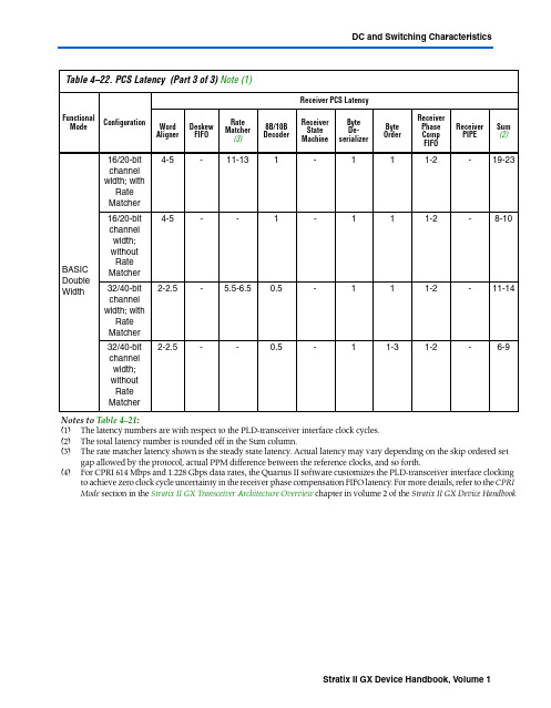
BASIC Double Width 16/20-bitchannelwidth; withRateMatcher4-5-11-131-111-2-19-2316/20-bitchannelwidth;withoutRateMatcher4-5--1-111-2-8-1032/40-bitchannelwidth; withRateMatcher2-2.5- 5.5-6.50.5-111-2-11-1432/40-bitchannelwidth;withoutRateMatcher2-2.5--0.5-11-31-2-6-9Notes to Table 4–21:(1)The latency numbers are with respect to the PLD-transceiver interface clock cycles.(2)The total latency number is rounded off in the Sum column.(3)The rate matcher latency shown is the steady state latency. Actual latency may vary depending on the skip ordered set gap allowed by the protocol, actual PPM difference between the reference clocks, and so forth.(4)For CPRI 614 Mbps and 1.228 Gbps data rates, the Quartus II software customizes the PLD-transceiver interface clockingto achieve zero clock cycle uncertainty in the receiver phase compensation FIFO latency. For more details, refer to the CPRI Mode section in the Stratix II GX Transceiver Architecture Overview chapter in volume 2 of the Stratix II GX Device HandbookTable 4–22.PCS Latency (Part 3 of 3) Note (1)Functional Mode Configuration Receiver PCS LatencyWordAligner Deskew FIFO Rate Matcher(3)8B/10B Decoder Receiver StateMachine Byte De-serializer Byte Order Receiver Phase CompFIFO Receiver PIPE Sum (2)50-Ω R T2.5Internal parallel termination with calibration (50-Ω setting )V CCIO = 1.8 V ±30± 30%25-Ω R S1.8Internal series termination with calibration (25-Ω setting )V CCIO = 1.8V ±5±10%Internal series termination without calibration (25-Ω setting )V CCIO = 1.8V ±30±30%50-Ω R S 1.8Internal series termination with calibration (50-Ω setting )V CCIO = 1.8 V ±5±10%Internal series termination without calibration (50-Ω setting )V CCIO = 1.8V ±30±30%50-Ω R T 1.8Internal parallel termination with calibration (50-Ω setting )V CCIO = 1.8V ±10±15%50-Ω R S 1.5Internal series termination with calibration (50-Ω setting )V CCIO = 1.5V ±8±10%Internal series termination without calibration (50-Ω setting )V CCIO = 1.5V ±36±36%50-Ω R T 1.5Internal parallel termination with calibration (50-Ω setting )V CCIO = 1.5V ±10±15%50-Ω R S 1.2Internal series termination with calibration (50-Ω setting )V CCIO = 1.2V ±8±10%Internal series termination without calibration (50-Ω setting )V CCIO = 1.2V ±50±50 %50-Ω R T1.2Internal parallel termination with calibration (50-Ω setting )V CCIO = 1.2V ±10±15%Note for Table 4–49:(1)The resistance tolerance for calibrated SOCT is for the moment of calibration. If the temperature or voltage changes over time, the tolerance may also change.(2)On-chip parallel termination with calibration is only supported for input pins.Table 4–49.On-Chip Termination Specification for Top and Bottom I/O Banks (Part 2 of 2) Notes (1), (2)SymbolDescription Conditions Resistance ToleranceCommercial Max Industrial Max UnitStratix II GX Architecture Figure2–2.Elements of the Transceiver BlockEach Stratix II GX transceiver channel consists of a transmitter and receiver. The transceivers are grouped in four and share PLL resources. Each transmitter has access to one of two PLLs. The transmitter contains the following:■Transmitter phase compensation first-in first-out (FIFO) buffer■Byte serializer (optional)■8B/10B encoder (optional)■Serializer (parallel-to-serial converter)■Transmitter differential output bufferThe receiver contains the following:■Receiver differential input buffer■Receiver lock detector and run length checker■Clock recovery unit (CRU)■Deserializer■Pattern detector■Word aligner■Lane deskew■Rate matcher (optional)■8B/10B decoder (optional)■Byte deserializer (optional)■Byte ordering■Receiver phase compensation FIFO bufferDesigners can preset Stratix II GX transceiver functions using the Quartus®II software. In addition, pre-emphasis, equalization, and differential output voltage (V OD) are dynamically programmable. EachStratix II GX transceiver channel supports various loopback modes and is。

Phoenix-32HP32 Channel 1.5U H.265 Network Video Recorder●Smart H.265+/H.265/Smart H.264+/H.264●Up to 8MP(4K) resolution preview & playback ●Up to 32 channel IP camera inputs, 16 port PoE ●Up to 2ch@4K/8ch@1080P decoding ●Max 200Mbps Incoming Bandwidth ●HDMI/VGA simultaneous video output●Support 4 SATA HDD up to 6TB, 2USB (2.0,3.0)InteroperabilityThe camera conforms to the ONVIF (Open Network Video Interface Forum) specifications, ensuring interoperability between network video products regardless of manufacturer.Flexible RecordingThe AVR offers a variety of configurable recording options and schedule that saves HDD space and active monitoring time. The recorder monitors incoming video and can be programmed to record if motion is detected or if an alarm is triggered. The recorder can also be programmed to record on a schedule or at different intervals. The recording options and schedules can be set for each individual camera or copied to all cameras..Clearview’s newest generation Phoenix-32HP providesexcellent performance at an affordable price. For applications where image details are highly required, it delivers thecapability of 4K resolution processing. This 32 channel NVR features an 16 port built in PoE and new Smart H.265+ decoding technology, saving up to 50% HDD and storage space compared to traditional H.264.The NVR is compatible with numerous third-party devices making it the perfect solution for surveillance systems that work independently of video management system (VMS). It features an open architecture that supports for multi-user access and is compatible with ONVIF 2.4 protocol, enabling interoperability with many different IP cameras.System OverviewFunctionsSmart H.265+Smart H.265+ is the optimized implementation of theH.265 codec that uses a scene-adaptive encoding strategy, dynamic GOP, dynamic ROI, flexible multi-frame reference structure and intelligent noise reduction to deliverhigh-quality video without straining the network. Smart H.265+ technology reduces bit rate and storagerequirements by up to 70% when compared to standard H.265 video compression.4K resolution4K resolution is a revolutionary breakthrough in image processing technology. 4K delivers four times theresolution of standard HDTV 1080p cameras and offers superior picture quality and image detail. 4K resolution improves the clarity of a magnified scene to view or record crisp forensic video from large areas.Technical SpecificationOSD Menu SupportVideo Interface N/AAudio Interface N/ARS485N/A AlarmN/AElectrical Main Processor Quad-core embedded processor Operating SystemEmbedded LINUXSystemVideo/Audio Compression Smart H.265+/H.265/Smart H.264+/H.264Image Resolution 8MP/6MP/5MP/4MP/3MP/1080P/ 720P/ D1&etc.Record Rate 200MbpsBit Rate 16Kbps ~ 20Mbps Per ChannelRecord Mode Manual, Schedule(Regular(Continuous), MD, Alarm), StopRecord Interval1~120 min (default: 60 min), Pre-record: 1~30 sec, Post-record: 10~300 secRecordingIP Video Input32 channelVideoInput N/A Output N/ATwo-way Talk1 channel Input, 1 channel Output, RCAAudioDisplayTrigger Events Recording, PTZ, Tour, Video Push, Email, FTP, Snapshot, Buzzer & Screen tipsVideo Detection Motion Detection, MD Zones: 396(22×18), Video Loss & Camera Blank Alarm Input 16 Channel Relay Output4 ChannelInterface 1 HDMI ,1 VGAResolution HDMI: 3840×2160, 1920×1080, 1280×1024, 1280×720VGA: 1920×1080, 1280×1024, 1280×720Decoding Capacity2ch@4K 30fps, 8ch@1080P 30fps Display Split1/4/8/9/16/25/36OSDCamera title, Time, Video loss, Camera lock, Motion detection, RecordingVideo Detection & AlarmSync Playback 1/4/9/16Search Mode Time/Date, Alarm, MD & Exact search (accurate to second), Smart search Playback Functions Play, Pause, Stop, Rewind, Fast play, Slow play, Next file, Previous file, Next camera, Previous camera, Full screen, Repeat, Shuffle, Backup selection, Digital zoom Backup ModeUSB Device/NetworkPlayback & BackupEthernet 1 RJ-45 port (10/100/1000Mbps)PoE16 ports (IEEE802.3at/af)Network Functions HTTP, TCP/IP, IPv4/IPv6, UPNP, RTSP, UDP, SMTP, NTP, DHCP, DNS, IP Filter, PPPOE, DDNS, FTP, Alarm Server, IP Search, P2P Max. User Access128 usersSmart Phone Android, iOS, iPhone InteroperabilityONVIF 2.4, SDK, CGINetworkUSB2 ports(1 USB2.0, 1 USB3.0)RS232 1 Port, for PC Communication and Keyboard RS4851 Port, for PTZ ControlAuxiliary InterfaceInternal HDD 4 SATA Port, up to 6TB capacity External HDDN/AStoragePower Supply AC100V ~ 240V, 50 ~ 60 HzPower Consumption NVR: < 13.7W(without HDD)PoE: Max 25.5w for single port, 150w in total Working Environment -10°C ~ +55°C (+14°F ~ +131°F), 86 ~ 106kpa Dimensions (W×D×H) 1.5U, 440mm×411.1mm×76mm (17.3" x 16.2" x 3.0")Net Weight 4.7kg (10.4lb) (without HDD)Gross Weight7.5kg(16.5 lb)(without HDD)GeneralRecordingCertificationsEN55032, EN55024, EN50130-4, EN60950-1Part 15 Subpart B, ANSI C63.4-2014UL60950-1CertificationsDimensions (mm/in)。

研华256主板说明书【实用版】目录1.研华 256 主板概述2.主板特性3.规格参数4.安装与设置5.使用注意事项6.保修与联系方式正文【研华 256 主板概述】研华 256 主板是一款性能卓越、稳定可靠的计算机主板,适用于各种计算需求,如办公、图像处理、游戏等。
它采用了先进的制造工艺和顶级的元器件,为用户提供了一个高效的计算平台。
【主板特性】研华 256 主板具有以下特性:1.支持英特尔酷睿处理器,性能强大。
2.支持 DDR4 高速内存,提升数据传输速度。
3.集成显卡,支持高清显示。
4.多个 PCIe 插槽,可扩展显卡、存储等设备。
5.丰富的扩展接口,方便连接各种外部设备。
6.板载高速存储,提高系统响应速度。
【规格参数】研华 256 主板的主要规格参数如下:1.处理器:支持英特尔酷睿 i3/i5/i7 处理器。
2.内存:支持 DDR4 2133/2400/2666MHz内存,最大容量32GB。
3.显卡:集成显卡,支持 HDMI 和 DisplayPort 接口。
4.存储:支持 SATA 和 PCIe NVMe 硬盘,最大容量 2TB。
5.扩展接口:包括 USB 3.0、HDMI、DisplayPort、LAN、音频等接口。
6.PCIe 插槽:2 个 PCIe 3.0 x16 插槽,1 个 PCIe 3.0 x8 插槽。
【安装与设置】在安装研华 256 主板时,请按照以下步骤进行:1.确认主板与机箱的兼容性。
2.将主板放入机箱,连接电源线、电源按键和复位按键。
3.安装处理器、内存和显卡等设备。
4.连接硬盘、光驱、USB 设备等。
5.接通电源,启动计算机。
6.进入 BIOS 设置,调整相关参数。
【使用注意事项】在使用研华 256 主板时,请注意以下几点:1.请勿超频处理器,以免损坏主板。
2.请使用正品内存和显卡,以确保系统稳定。
3.在连接外部设备时,请确保接口正确,避免短路。
4.定期检查系统运行状况,及时发现并解决问题。

Arduino的详细介绍(基于Mega2560)很早之前入手了一块Arduino Mega2560,当时只是认为其操作简单且更加人性化,开源方便,想了解了解。
最新搞项目想用Arduino试试控制8路舵机,但网上找的Servo库大多说只支持9,10接口,很是恼火(资料怎么写就怎么搬,到底是不是只支持9,10接口有几个知道?又有几个知道为什么?)。
另外本人长期逛各种论坛,发现国内民间创客极客水平还是普遍低下的,Arduino虽说开源但国内确实找不到多少参考资料,这无形之中成了小小的阻碍,于是本人花了点时间为广大Arduino爱好者整理翻译此份资料,一是想丰富网上资源,二是以一种更加简便的方式带部分人入门。
了解原理才能谈创意,不求甚解只能做个小玩家。
了解Arduino的最好平台当然是官网,我相信官网肯定不会遗漏自己产品最有特色的东西,因此以它为参考绝对没错。
另外,必要部分辅助以百科,以及各位广大亲爱博友的资料(就不一一列举了,在此谢过)。
本文以Arduino Mega 2560为基础解释,其他板子都差不多。
一:概述Arduino Mega 2560是基于ATmega2560的微控制板,有54路数字输入/输出端口(其中15个可以作为PWM输出),16路模拟输入端口,4路UART串口,16MHz的晶振,USB连接口,电池接口,ICSP头和复位按钮。
简单地用USB连接电脑或者用交直流变压器就能使用。
Mega 2560 是Arduino Mega系列的升级版。
Mega 2560与之前的板子(最大)不同在于:它没用FTDI USB-to-serial驱动芯片,而是用ATmega16U2编程作为USB-to-serial传输器(V1版本使用8U2)。
总结如下:二:电源这部分就不说了,涉及3.3v和5v供电。
三:存储器ATmega2560有256k的闪存可存储程序(其中8kb用作bootloader),有8kb的SRAM和4kb的EEPROM(可使用EEPROM library(点击看详细介绍)进行读写)。

耳机3000 系列TAT3256用户手册访问以下网站注册您的产品并获取支持/support目录1 重要安全说明 2听力安全 2一般信息 22 纯无线耳机 3包装盒内物品 3其他设备 3纯蓝牙无线耳机概述 43 使用入门 5电池充电 5首次将耳机与蓝牙设备配对 5将耳机与另一个蓝牙设备配对 64 使用耳机 7将耳机连接至蓝牙设备 7开机/关机 7管理通话和音乐 7LED 指示灯状态 8语音助手 85 重置耳机 96 技术数据 107 注意 11符合性声明 11旧产品和电池的处理 11拆除集成式电池 11符合电磁场 (EMF) 法规 12环保信息 12法规遵循注意事项 128 商标 149 常见问题解答 15CN 11 重要安全说明听力安全危险• 为避免听力受损,应限制以高音量使用耳机的时间,并将音量设定在安全级别。
音量越大,安全收听的时间越短。
使用耳机时请确保遵循以下准则。
• 在合理时间内以合理音量收听。
• 听力适应后,注意不要持续地调高音量。
• 请勿将音量调得太高而使得无法听见周围的声音。
• 在有潜在危险的情况下应谨慎使用或暂停使用。
• 耳机声压过大可导致听力受损。
• 建议在驾车时不要双耳佩戴耳机,而且在某些地区这样做可能属于违法行为。
• 出于安全考虑,在驾车时或其它存在潜在危险的环境下,应避免让音乐或通话分散您的注意力。
一般信息为避免损坏或故障:警告• 切勿将耳机置于高温环境• 切勿摔落耳机• 切勿将耳机置于滴水或溅水环境下。
• 切勿将耳机没入水中。
• 切勿使用任何包含酒精、氨水、苯或研磨剂的清剂清洁产品。
• 如果需要,请使用软布清洁产品,可用少量的水或稀释的中性肥皂水将布打湿进行清洁。
• 切勿将集成式电池置于高温环境,如阳光直射处、明火或类似环境。
• 如果电池更换不当,会有爆炸危险。
仅使用相同或同等类型的电池进行更换。
•如果将电池投入火中或热烤箱中,或将其机械压碎或切割,会导致爆炸;•如果将电池放在极高温度环境中,会导致爆炸或易燃液体或气体泄漏;•如果将电池放在极低气压环境中,可能会导致爆炸或易燃液体或气体泄漏。

Hi3536 H.265 Decoder Processor Brief Data SheetIssue 03Date 2015-04-19Copyright © HiSilicon Technologies Co., Ltd. 2014. All rights reserved.No part of this document may be reproduced or transmitted in any form or by any means without prior written consent of HiSilicon Technologies Co., Ltd.Trademarks and Permissions, , and other HiSilicon icons are trademarks of HiSilicon Technologies Co., Ltd.All other trademarks and trade names mentioned in this document are the property of their respective holders.NoticeThe purchased products, services and features are stipulated by the contract made between HiSilicon and the customer. All or part of the products, services and features described in this document may not be within the purchase scope or the usage scope. Unless otherwise specified in the contract, all statements, information, and recommendations in this document are provided "AS IS" without warranties, guarantees or representations of any kind, either express or implied.The information in this document is subject to change without notice. Every effort has been made in the preparation of this document to ensure accuracy of the contents, but all statements, information, and recommendations in this document do not constitute a warranty of any kind, express or implied.HiSilicon Technologies Co., Ltd.Address: Huawei Industrial BaseBantian, LonggangShenzhen 518129People's Republic of ChinaWebsite: Email: support@Hi3536 Key SpecificationsProcessor Corez ARM Cortex A17 quad-core@maximum 1.4 GHz −32 KB L1 I-cache, 32 KB L1 D-cache− 1 MB L2 cache−Main control processor for running peripheral driversand applicationsz ARM Cortex A7 single-core@maximum 900 MHz −32 KB L1 I-cache, 32 KB L1 D-cache−128 KB L2 cache−Video-related module controlVideo Decoding Standardsz H.265 Main Profile L5.1z H.264 Baseline/Main/High profile L5.0z MPEG4 SP L0–3/ASP L0–5z MJPEG/JPEG baselineVideo Encoding Standardsz H.264 Baseline/Main/High profile L5.1z MJPEG/JPEG baselineVideo Encoding/Decodingz H.265/H.264&JPEG encoding and decoding of multiple streams:−4-channel 4K x 2K (3840 x 2160)@30 fpsH.265/H.264 decoding+2x1080p@30 fps H.264encoding+4-channel 4K x 2K@2 fps JPEG encoding −16x1080p@30 fps H.265/H.264decoding+2x1080p@30 fps H.264encoding+16x1080p@2 fps JPEG encoding−9x1080p@30 fps H.265/H.264 decoding+4K x2K@30 fps H.264 encoding+9x1080p@2 fps JPEGencoding−32x720p@30 fps H.265/H.264 decoding+4x720p@30 fps H.264 encoding+32x720p@2 fps JPEG encoding −64xD1@30 fps H.265/H.264 decoding+8xD1@30 fpsH.264 encoding+64xD1@2 fps JPEG encoding−9x720p@30 fps JPEG decodingz CBR or VBR, ranging from 16 kbit/s to 40 Mbit/sz Encoding frame rate ranging from 1 fps to 60 fpsz ROI encodingz Color-to-gray encodingGPUz Integrated Mali-T720 GPUz OpenGL ES3.1/2.0/1.1z OpenCL 1.2/1.1/1.0z Up to 63 MTris/s triangle filling ratez Double-precision FP64 and anti-aliasingIntelligent Video Analysisz Integrated IVE 2.0, supporting various intelligent analysis applications:−Motion detection−Video diagnosis−Perimeter protection Video and Graphic Processingz3D denoising, deinterlacing, edge smoothing, dynamic contrast enhancement and sharpeningz Anti-flicker for output videos and graphicsz1/8x to 16x video scalingz1/2x to 2x graphic scalingz Four cover regionsz OSD overlaying of eight regionsVideo Interfacesz VI interfaces−One BT.1120 HD input port−One video input channel for dual-chip cascading−SDR and DDR modes−Maximum input of 1080p@60 fps in SDR mode−Maximum input of 3840 x 2160@30 fps in DDRmodez VO interfaces−One HDMI 2.0 ultra-HD output interface, supportoutput up to 3840 x 2160@60 fps−One VGA HD output interface, support output up to2560 x 1600@60 fps−One BT.1120 HD output port, supporting themaximum output of 1080p@60 fps in SDR mode or3840 x 2160@30 fps in DDR mode−Two independent HD output channels (DHD0 andDHD1), output from any HD interface (HDMI, VGA,and BT.1120)−64-picture output for DHD0, maximum 3840 x2160@60 fps output−32-picture output for DHD1, maximum 1080p@60fps output−One CVBS SD output interface−Three full-screen GUI graphics layers in RGB1555or RGB8888 format, used by two HD channels andone SD channel−Two hardware cursor layers in RGB1555, RGB4444or RGB8888 format, with the maximum resolution of256 x 256Audio Interfacesz One integrated audio CODECz Three unidirectional I2S/PCM interfaces−One input, supporting 16 multiplexed inputs−Two outputsz16-bit audio input and outputEthernet Portsz Two gigabit Ethernet ports−RGMII, RMII, and MII modes−10/100 Mbit/s full-duplex or half-duplex−1000 Mbit/s full-duplex−TOE for reducing the CPU usageSecurity Enginez AES, DES, 3DES algorithmsz HASH abstract algorithmRAID Acceleration Enginez XOR accelerationz Up to nine data sources for XORz DMA, up to 16 MB data blockz Memory initialization (configurable initial value)z Descriptor linked listPeripheral Interfacesz Two SATA 3.0 interfaces−PM−eSATAz One PCIe 2.0/SATA 3.0 interfaces−Two PCIe interfaces, one PCIe interface+one SATAinterface, or two SATA interfaces−RC and EP supported as the PCIe 2.0 interface−eSATA supported as the SATA 3.0 interfacez Two USB 2.0 host ports, supporting hubz One USB 3.0 host port, supporting hubz Two SDIO interfaces−SD 2.0, SDIO 2.0, MMC 4.4.1, and SDXC (only 3.3V mode) cards supported for SDIO0 and SDIO1−Only eMMC 4.5 card supported for SDIO1−Multiplexing between SDIO0 and BT.1120 outputpins−Multiplexing between SDIO1 and NAND flashinterface pinsz Four UART interfaces, two of which supporting four wiresz One IR interfacez One I2C interfacez Multiple GPIO interfacesz One low-speed ADC interfaceMemory Interfacesz Two 32-bit DDR3/4 SDRAM interfaces−Maximum frequency of 933 MHz (1.866 Gbit/s)−Dual channels−ODT−Maximum capacity of 3 GBz SPI NOR/NAND flash interface−1-/2-/4-bit SPI NOR/NAND flash−Two CSs−Maximum 32 MB for each CS (for only the NORflash)−Maximum 8 GB for each CS (for only the NANDflash)−2 KB/4 KB page size (for only the NAND flash)−8-bit/1 KB and 24-bit/1 KB ECC (for only theNAND flash)z NAND flash interface−8-bit NAND flash−Two CSs−SLC or MLC−8-/24-/40-/64-bit ECC based on the 1 KB data block z Embedded 64 KB BOOTROM and 88 KB SRAM RTC with an Independent Power Supplyz Independent battery for supplying power to the RTC Boot Modesz Booting from the BOOTROMz Booting from the SPI NOR flashz Booting from the SPI NAND flashz Booting from the NAND flashz Booting from the eMMCz Booting the slave chip over the PCIe interfaceSDKz Linux 3.10-based SDKz Audio encoding and decoding libraries complying with various protocolsz High-performance H.265/H.264 PC decoding library Physical Specificationsz Power consumption−Typical power consumption of 4.3 W−Multi-level power-saving controlz Operating voltages−0.9 V core voltage−1.0 V CPU voltage (or decreased to 0.9 V)−3.3 V I/O voltage−1.5/1.2 V DDR3/4 SDRAM interface voltagez Package−RoHS, EDHS-PBGA−Ball pitch of 0.8 mm (0.02 in.)−Body size of 27 mm x 27 mm (1.06 in. x 1.06 in.) z Operating temperature ranging from 0°C (32°F) to 70°C (158°F)Functional Block DiagramThe Hi3536 is a professional high-end SoC targeted for the multi-channel HD or D1 NVR. The Hi3536 provides a high-performance A 17 processor, a video decoding engine (a maximum of 16x1080p decoding complying with various protocols), a high-performance video/graphics processing engine (various complicated graphics processing algorithms), and dual-channel HD outputs. These features enable the Hi3536 to provide high-quality images. In addition, the Hi3536 integrates various peripheral interfaces to meet differentiated customer requirements for functionality, features, and image quality, while reducing the eBOM cost.NVRs (Each with a Hi3536)16x1080p NVRz32x1080p@10 Mbit/s streamsz16x1080p real-time decoding (16-channel polling previewing)z2x1080p real-time encodingz1080p@32 fps JPEG snapshotz HDMI 4K x 2K@30 fps 16-picture ultra-HD output32x720p NVRz64x720p@5 Mbit/s streamsz32x720p real-time decoding (32-channel polling previewing)z4x720p real-time encodingz 720p@64 fps JPEG snapshotzHDMI+VGA 1080p@60 fps HD dual 16-picture output 64xD1 NVRz 128x D1@2.5 Mbit/s streamsz 64xD1 real-time decoding (64-channel real-time previewing) z 8xD1 real-time encoding z D1@128 fps JPEG snapshotzHDMI 4K x 2K@30 fps 64-picture ultra-HD outputGMACVGAHDMIGMAC0IP cameraLAN/WANBT.1120DDR CtrlI 2SGE PHY port multiplierHDMI PHY...Acronyms and Abbreviationsdataencryption standard3DES triplestandardencryptionAES advancedCBR constant bit rateselectCS chipvideo broadcast signalCVBS compositerateDDR double-datastandardencryptionDES dataDMA direct memory accessECC error correcting codeEP endpointadvanced technology attachmentserialeSATA externalinput/output GPIO general-purposeGUI graphical user interfaceHD high-definitionHDMI high-definition multimedia interfaceI2C inter-integratedcircuitI2S inter-ICsoundIR infraredenginevideoIVE intelligentMII media independent interfacecellMLC multi-levelNVR network video recorderterminationODT on-diedisplayOSD on-screenPBGA plastic ball grid arraycomponent interconnect expressPCIe peripheralPM portmultiplexerRAID redundant array of independent diskscomplexRC rootRGMII reduced gigabit media independent interfaceRMII reduced media independent interfaceRoHS restriction of the use of certain hazardous substances ROI region of interestclockRTC real-timetechnology attachmentadvancedSATA serialSD standard-definitionSDR single data rateSDK software development kitSDRAM synchronous dynamic random access memorySHA secure hash algorithmcellSLC single-levelSMMU system memory management unitSoC system-on-chipSP simpleprofileinterfaceperipheralSPI serialSRAM static random access memoryoffloadengineTOE TCP/IPUART universal asynchronous receiver transmitterVBR variable bit rateVGA video graphics arrayoutputVO video。