NRLMW332M160VF中文资料
- 格式:pdf
- 大小:57.57 KB
- 文档页数:3

Figure 33: WRITE Burst Followed by PRECHARGE – WL = 1, BL = 4Transitioning dataAuto PrechargeBefore a new row can be opened in an active bank, the active bank must be precharged using either the PRECHARGE command or the auto precharge function. When a READ or WRITE command is issued to the device, the auto precharge bit (AP) can be set to enable the active bank to automatically begin precharge at the earliest possible mo-ment during the burst READ or WRITE cycle.If AP is LOW when the READ or WRITE command is issued, then normal READ or WRITE burst operation is executed and the bank remains active at the completion of the burst.If AP is HIGH when the READ or WRITE command is issued, the auto precharge func-tion is engaged. This feature enables the PRECHARGE operation to be partially or com-pletely hidden during burst READ cycles (dependent upon READ or WRITE latency),thus improving system performance for random data access.READ Burst with Auto PrechargeIf AP (CA0f) is HIGH when a READ command is issued, the READ with auto precharge function is engaged.These devices start an auto precharge on the rising edge of the clock BL/2 or BL/2 - 2 +RU(t RTP/t CK) clock cycles later than the READ with auto precharge command, which-ever is greater. For auto precharge calculations, see the PRECHARGE and Auto Pre-charge Clarification table.I DD SpecificationsTable 4: 64 Meg x 16 I DD Specifications1Gb: x16, x32 Automotive Mobile LPDDR2 SDRAM I DD Specifications。

Large Can Aluminum Electrolytic CapacitorsFEATURES• NEW SIZES FOR LOW PROFILE AND HIGH DENSITY DESIGN OPTIONS • EXPANDED CV VALUE RANGE• HIGH RIPPLE CURRENT• LONG LIFE • CAN-TOP SAFETY VENT• DESIGNED AS INPUT FILTER OF SMPS • STANDARD 10mm (.400") SNAP-IN SPACING NRLM SeriesSPECIFICATIONS(* 47,000µF add 0.14, 68,000µF add 0.35.)Notice for MountingThe space from the top of the can shall be more than (3mm) from chassis or other construction materials so that safety vent has room to expand in case of emer g en c y.Sleeve Color: DarkBlueCan Top Safety VentInsulation Sleeve and Minus Polarity Marking(4.0mm Leads Available As Option)D+1Max.L ± 26.3 ± 10.810(-)(+)MAXIMUM EX P AN S IONFOR SAFETY VENT Approx. 3.0mmRecommended PC Board Mounting Holes:10 ± .1∅= 2 ± 0.1D ∅ ± 0.5ChassisPC BoardPRECAUTIONSPlease review the notes on correct use, safety and precautions found on pages T10 & T11of NIC’s Electrolytic Capacitor catalog . Operating Temperature Range-40 ~ +85°C-25 ~ +85°C Rated Voltage Range 16 ~ 250Vdc 350 ~ 450Vdc Rated Capacitance Range 180 ~ 68,000µF56 ~ 680µFCapacitance Tolerance ±20% (M)Max. Leakage Current (µA)After 5 minutes (20°C)3 x C(µF)VMax. Tan δat 120Hz/20°C W.V. (Vdc)162535506380100160~450Tan δ max.0.50*0.40*0.350.300.250.200.200.15Surge VoltageW.V. (Vdc)162535506380100160S.V. (Vdc)2032446379100125200W.V. (Vdc)180200250350400450--S.V. (Vdc)220250300400450500--Ripple CurrentCorrection Factors Frequency (Hz)50601001205001K 10K ~ 50K -Multiplier at 85°C0.750.800.95 1.00 1.05 1.08 1.15-Low TemperatureStability (10 to 250Vdc)Temperature (°C)0-25-40-----Capacitance Change-5%-15%-30%-----Impedance Ratio 1.539-----Load Life Test2,000 hours at +85°CCapacitance ChangeWithin ±20% of initial measured value Tan δLess than 200% of specifi ed maximum valueLeakage Current Less than specifi ed maximum value Shelf Life Test1,000 hours at +85°C (no load)Capacitance Change Within ±20% of initial measured value Tan δLess than 200% of specifi ed maximum valueLeakage Current Less than specifi ed maximum value Surge Voltage Test Per JIS-C-5141 (table #6, #4)Surge voltage applied: 30 seconds"On" and 5.5 minutes no voltage "Off"Capacitance Change Within ±20% of initial measured value Tan δLess than 200% of specifi ed maximum valueLeakage Current Less than specifi ed maximum value Soldering EffectRefer to MIL-STD-202F Method 210A Capacitance Change Within ±10% of initial measured valueTan δLess than specifi ed maximum value Leakage CurrentLess than specifi ed maximum valueRoHS Compliantincludes all homogeneous materials*See Part Number System for DetailsLarge Can Aluminum Electrolytic CapacitorsNRLM SeriesNRLM 222 M 50V 20X25 FRoHS compliant Case Size (mm) Voltage Rating Tolerance Code PART NUMBER SYSTEMLarge Can Aluminum Electrolytic Capacitors NRLM Series STANDARD PRODUCT LIST, CASE SIZE AND SPECIFICATIONS。


维 修 手 册00ZARM205/A2C 数码复合机MODEL AR-M160 AR-M205目 录[1] 概 要[2] 规 格[3] 消耗品[4] 外观和内部结构[5] 开箱和安装[6] 调 整[7] 模拟代码[8] 用户程序[9] 故障代码[10] 维修保养[11] 分解组装[12] 电路部分1 - 12 - 13 - 14 - 15 - 16 - 17 - 18 - 19 - 110 - 111 - 112 - 1为确保安全性、可靠性,更换部品务必使用正规品。
指定的部品。
本手册仅供维修人员进行售后服务用,SHARP CORPORATION目录[ 1 ] 概 要1. 维修注意事项.....................................................1 - 1[ 2 ] 规 格1. 复印模式............................................................2 - 1[ 3 ] 消耗品1. 消耗品供应表.....................................................3 - 12. 使用环境............................................................3 - 1[ 4 ] 外观和内部结构1. 外 观................................................................4 - 12. 内部结构............................................................4 - 23. 操作面板............................................................4 - 34. 电机,电磁铁,离合器.......................................4 - 45. 传感器,开关.....................................................4 - 56. 电路板组件.........................................................4 - 67. 剖面图................................................................4 - 7[ 5 ] 开箱和安装1. 安装条件............................................................5 - 12. 去除保护材料和固定螺钉...................................5 - 13. 安装步骤............................................................5 - 14. 固定螺钉的卸除和保存.......................................5 - 35. 纸盒纸张尺寸设置..............................................5 - 3[ 6 ] 调 整1. 调整项目表.........................................................6 - 12. 复印机调整.........................................................6 - 1[ 7 ] 模拟代码1. 进入模拟代码.....................................................7 - 12. 解除模拟代码.....................................................7 - 13. 模拟代码列表.....................................................7 - 14. 模拟代码详细内容..............................................7 - 3[ 8 ] 用户程序1. 用户程序列表......................................................8 - 12. 设置用户程序......................................................8 - 43. 墨粉盒使用寿命..................................................8 - 4[ 9 ] 模拟代码表1. 故障代码表.........................................................9 - 12. 故障代码具体说明..............................................9 - 1[ 10 ] 维修保养1. 维修保养明细表................................................10 - 12. 维修保养显示系统............................................10 - 23. 更换消耗品部件注意事项..................................10 - 2[ 11 ] 分解和组装1. 高压部分/双面输送部分....................................11 - 12. 光学部分...........................................................11 - 23. 定影部分...........................................................11 - 44. 出纸部分...........................................................11 - 65. MCU部件..........................................................11 - 86. 光学结构组件....................................................11 - 87. LSU组件...........................................................11 - 88. 纸盒进纸部分/纸张传输部分.............................11 - 99. 手送进纸部分..................................................11 - 1010. 电源部分.......................................................11 - 1211. 显影部分.......................................................11 - 1312. 成像部分.......................................................11 - 1413. 其他..............................................................11 - 15[ 12 ] 电路部分1. 结构框图...........................................................12 - 12. 电路说明...........................................................12 - 23. 实际线路图.......................................................12 - 5[ 1 ] 概 要1. 维修注意事项指示图:机器的定影区域带有 () 标签的地方意思如下: : 小心,有危险。

我们知道雷蒙磨粉机是一种很好的高细粉磨设备,也是许多矿业企业深加工的重要设备之一,由于是大型的设备,而且不同厂家的设备型号也是有一定区别的,这样的话才能便于客户更好地区分,下面就主要的雷蒙磨设备型号为大家介绍如下。
雷蒙磨规格有3R、4R、5R、6R,其实R就是英文Roller,即是磨辊;3、4、5、6表示数量,所以3R代表3个磨辊,4R代表4个磨辊。
比如4R3216雷蒙磨就是,磨辊有4个,磨辊直径为320mm,磨辊高度为160mm,磨环内径为970mm,磨环高度为160mm。
3r雷蒙磨:3R2615 3 260×150 Ф780 <15 <30-325 <0.8-2.5 18.5 15 2.2 5650×3305×5950 3R2715 3 270×150 Ф830 <15 <30-325 <0.9-2.8 22 18.5 2.2 8000×3500×4900 3R3016 3 300×160 Ф880 <20 <30-325 <1.1-4 30 22 3 6500×4100×5200 4R3216 4 320×160 Ф970 <20 <30-325 <1.8-4.5 37 30 5.5 9900×5800×10580 5R、6R雷蒙磨:雷蒙磨的选型也是很重要的,用户应该根据实际生产需求合理选择型号。
设备对物料适用性强,可针对莫氏硬度9.3级以下的各种非易燃易爆矿产物料,成品粉子细度均匀,通筛率比其他的制粉设备高。
不同型号之间的性能有所差别,大家需要仔细对比。
雷蒙磨是适合中小型生产线的磨粉机,经过多次改进,该机产量可观,优势明显,受到了市场肯定,适用于冶金、建材、化工、矿山等矿产品物料的粉磨加工。

White Electronic DesignsWC16P332-16GXPRELIMINARY*68020 Monolithic Microcontroller also available. Please call factory for more information.FEATURES100% CMOS16 MHz Operating Frequency Single 5V Operation System Integration Module (SIM)• External Bus Support • Programmable Chip-Select Outputs • System Protection Logic• Watchdog Timer, Clock Monitor, and Bus Monitor • System Protection Logic• System Clock Based on 32.768kHz Crystal for Low Power Operation• Test/Debug Submodule for Factory/User Test and DevelopmentCentral Processing Unit (CPU)• Upward Object Code Compatible• New Instructions for Controller Applications • 32-Bit Architecture • Virtual Memory Implementation • Loop Mode of Instruction Execution • Table Lookup and Interpolate Instruction• Improved Exception Handling for Controller Applications • Trace on Change of Flow• Hardware Breakpoint Signal, Background Mode • Fully Static Operation Time Processor Unit (TPU)• Dedicated Microengine Operating Independently of CPU32• 16 Independent, Programmable Channels and Pins • Any Channel can Perform any Time Function• Two Timer Count Registers with Programmable Prescalers • Selectable Channel Priority Levels Queued Serial Module (QSM)• Enhanced Serial Communication Interface (SCI), Universal Asynchronous Receiver Transmitter (UART): Modulus Baud Rate, Parity• Queued Serial Peripheral Interface (SPI): 80-Byte RAM, Up to 16 Automatic Transfers • Dual Function I/O Ports • Continuous Cycling, 8-16 Bits per TransferStatic RAM Module with TPU Emulation Capability (TPURAM)• 2-Kbytes of Static RAM• May be Used as Normal RAM or TPU Microcode Emulation RAMOperating Temperature Range -55°C to 125°C68332 MONOLITHIC MICROCONTROLLERPackaging• 132 lead, 24mm (0.950”) sq., Hermetic CQFP (Package 505) (shipped with leads cut and formed).DESCRIPTIONThe WC16P332 is a 32-bit microcontroller that includes high performance data manipulation features and peripheral subsystems. The WC16P332 is comprised of standard modules that interface through a common intermodule bus (IMB). The WC16P332 accommodates expedient development of devices which are tailored for specifi c applications.The M icrocontroller includes a 32-bit CPU (CPU32), a system integration module (SIM), a time processor unit (TPU), a queued serial module (QSM), and a 2Kx8 SRAM module with TPU emulation capability.The M icrocontroller can either synthesize an internal clock signal from an external reference or use an external clock input directly. Operation with a 32.768khz reference frequency is standard. System hardware and software allow changes in clock rate during operation. The Microcontroller module operation is fully static, therefore register and memory contents are not affected by clock rate changes.HCMOS technology makes the typical power consumption of the M icrocontroller low. Power consumption can be greatly decreased by stopping the system clock. The Microcontroller instruction set includes a low-power stop (LPSTOP) command that easily implements this feature.* T his product is under development, is not qualifi ed or characterized and is subject to change without notice.TYPICAL RATINGSNum Characteristic Symbol ValueUnit1Supply Voltage V CC5.0V 2V CC Supply CurrentI DD 75mA 3Clock Synthesizer Operating Voltage V CCSYN 5.0V 4V CCSYN Supply Current VCO on, maximum fsysExternal Clock, maximum fsys I DDSYN1.04.0mA mA 5RAM Standby Voltage V SB 3.0V 6RAM Standby Current Normal RAM operation Standby operation I SB7.040µA µA 7Power DissipationP D 455mWWhite Electronic DesignsWC16P332-16GXPRELIMINARYFIGURE 1 – PIN CONFIGURATION FOR WC16P332-16GX1819202122232425262728293031323334353637383940414243444546474849507161514131211101987654321231131031921821721621521421321221121021911811711V CC V STBY ADDR 1ADDR 2ADDR 3ADDR 4ADDR 5ADDR 6ADDR 7ADDR 8V CC V SS ADDR 9ADDR 10ADDR 11ADDR 12V SS ADDR 13ADDR 14ADDR 15ADDR 16V CC V SS ADDR 17ADDR 18PQS 0/MISO PQS 1/MOSI PQS 2/SCK PQS 3/PCS 0/SS#PQS 4/PCS 1PQS 5/PCS 2PQS 6/PCS 3V CCV S S S Q P 7D x T /D x R O S D /E P I P I I S D /H #C T E F I K L C S D /T #P K B C S T T O U Q /E Z E E R F V S S L A T X V N Y S D D L A T X E V C C C F X V C C T U O K L C V S S T #E S E R T #L A H R #R E B F P 7Q R I /7#F P 6Q R I /6F P 5Q R I /5F P 4Q R I /4F P 3Q R I /3F P 2Q R I /2F P 1Q R I /1#F P 0K L C D O M /W /R E P 7Z I S /1E P 6Z I S /0E P 5S A /V SS V CCBGACK/CS 2BG/CS 1BR/CS 0CSBOOT DATA 0DATA 1DATA 2DATA 3V CC V SS DATA 4DATA 5DATA 6DATA 7V SS DATA 8DATA 9DATA 10DATA 11V CC V SSDATA 12DATA 13DATA 14DATA 15ADDR 0PE 0/DSACK 0PE 1/DSACK 1PE 2/AVEC PE 3/RMC PE 4/DS V CCV S S H C U P T 0H C U P T 1H C U P T 2H C U P T 3H C U P T 4H C U P T 5H C U P T 6H C U P T 7V S S V C C H C U P T 8H C U P T 9H C U P T 01H C U P T 11V S S V C C H C U P T 21H C U P T 31H C U P T 41H C U P T 51T 2K L C V S S V C C R D D A 32S C /0#1C P 6R D D A /22S C /9#C P 5R D D A /12S C /8#C P 4R D D A /02S C /7#C P 3R D D A /91S C /6#C P 2C F /2S C /5#C P 1C F /1S C /4#C P 0C F /0S C /3#V SS 15253545556575859506162636465666768696071727374757677787970818283811611511411311211111010910810710610510410310210110099989796959493929190898887868584White Electronic Designs WC16P332-16GXPRELIMINARY PACKAGE 505: 132 LEAD, CERAMIC QUAD FLAT PACK, CQFP (G)ALL LINEAR DIMENSIONS ARE MILLIMETERS AND PARENTHETICALLY IN INCHESORDERING INFORMATIONW C 16 P332 - 16 G XDEVICE GRADE:M = Military Screened -55°C to +125°CI = Industrial -40°C to +85°CC = Commercial 0°C to +70°CPACKAGE:G = 132 Lead Ceramic Quad Flatpack, CQFP (Package 505)16MHz Operating Frequency6833216 bit WideMICROCONTROLLERWHITE MICROELECTRONICSWhite Electronic Designs WC16P332-16GXPRELIMINARY MANUFACTURING FLOW FOR WC16P332-16GM。


螺杆制冷机组说明书使用维护手册第一章总体介绍一、螺杆式制冷压缩机结构简介2二、螺杆式制冷压缩机压缩原理2三、压缩机技术参数3四、压缩机的油分离系统3五、压缩机的润滑油系统4六、压缩机的油冷却方式4七、内容积比和能量调节6八、经济器8九、机组流程图及技术参数表11第二章安装一、基础二、机组安装29三、管路连接29四、电机与压缩机的找正30五、机组排污与检漏33六、冷冻机油的加入33七、抽真空34八、制冷剂的加入34第三章操作、维护和保养一、操作35二、设备检修37三、长期停车的保养40四、故障指南40五、压缩机的检修第一章总体介绍一、螺杆式制冷压缩机结构简介本手册适用于我公司的螺杆III、II型机,其所列的螺杆式制冷压缩机系一种开启式双螺杆压缩机。
一对相互啮合的按一定传动比反向旋转的螺旋形转子,水平且平行配置于机体内部,具有凸齿的转子为阳转子,通常它与原动机连接,功率由此输入。
具有凹齿的转子称为阴转子。
在阴、阳转子的两端(吸气端和排气端)各有一只滚柱轴承承受径向力量,在两转子的排气端各有一只四点轴承,该轴承承受轴向推力。
位于阳转子吸气端轴颈尾部的平衡活塞起平衡轴向力减少四点轴承的负荷的作用。
在阴、阳转子的下部,装有一个由油缸内油活塞带动的能量调节滑阀,由电磁(或手动)换向阀控制,可以在15%~100%范围内实现制冷量的无级调节,并能保证压缩机处于低位启动,以达到小的启动扭矩,滑阀的工作位置可通过能量传感机构转换为能量百分数,并且在机组的控制盘上显示出来。
为了使螺杆压缩机运行时其外压比等于或接近机器的内压比,使机器耗功最小,压缩机内部设置了内容积比调节滑阀,由电磁(或手动)换向阀控制油缸内油的流动推动油活塞从而带动内容积比滑阀移动,其工作位置通过内容积比测定机构转换为内压力比值在机组的控制盘上显示出来。
螺杆式压缩机的结构见下图和本书后所附的压缩机剖面图。
螺杆式压缩机三维结构图二、螺杆式制冷压缩机压缩原理螺杆式制冷压缩属于容积式制冷压缩机,它利用一对相互啮合的阴阳转子在机体内作回转运动,周期性地改变转子每对齿槽间的容积来完成吸气、压缩、排气过程。
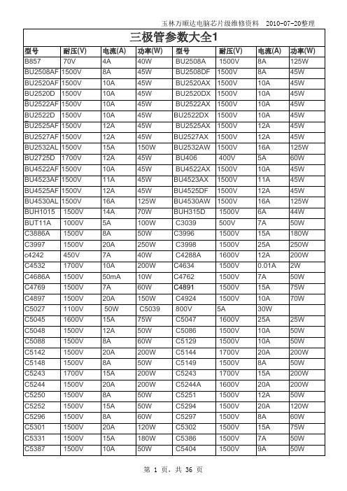
玉林万顺达电脑芯片级维修资料 2010-07-20整理玉林万顺达电脑芯片级维修资料 2010-07-20整理玉林万顺达电脑芯片级维修资料 2010-07-20整理玉林万顺达电脑芯片级维修资料 2010-07-20整理玉林万顺达电脑芯片级维修资料 2010-07-20整理玉林万顺达电脑芯片级维修资料 2010-07-20整理玉林万顺达电脑芯片级维修资料 2010-07-20整理玉林万顺达电脑芯片级维修资料 2010-07-20整理玉林万顺达电脑芯片级维修资料 2010-07-20整理玉林万顺达电脑芯片级维修资料 2010-07-20整理玉林万顺达电脑芯片级维修资料 2010-07-20整理玉林万顺达电脑芯片级维修资料 2010-07-20整理玉林万顺达电脑芯片级维修资料 2010-07-20整理玉林万顺达电脑芯片级维修资料 2010-07-20整理玉林万顺达电脑芯片级维修资料 2010-07-20整理玉林万顺达电脑芯片级维修资料 2010-07-20整理玉林万顺达电脑芯片级维修资料 2010-07-20整理玉林万顺达电脑芯片级维修资料 2010-07-20整理玉林万顺达电脑芯片级维修资料 2010-07-20整理玉林万顺达电脑芯片级维修资料 2010-07-20整理玉林万顺达电脑芯片级维修资料 2010-07-20整理玉林万顺达电脑芯片级维修资料 2010-07-20整理玉林万顺达电脑芯片级维修资料 2010-07-20整理玉林万顺达电脑芯片级维修资料 2010-07-20整理玉林万顺达电脑芯片级维修资料 2010-07-20整理玉林万顺达电脑芯片级维修资料 2010-07-20整理玉林万顺达电脑芯片级维修资料 2010-07-20整理玉林万顺达电脑芯片级维修资料 2010-07-20整理玉林万顺达电脑芯片级维修资料 2010-07-20整理玉林万顺达电脑芯片级维修资料 2010-07-20整理。


PRECHARGEThe PRECHARGE command is used to deactivate the open row in a particular bank orthe open row in all banks. The bank(s) will be available for a subsequent row activationa specified time (t RP) after the PRECHARGE command is issued, except in the case ofconcurrent auto precharge, where a READ or WRITE command to a different bank is al-lowed as long as it does not interrupt the data transfer in the current bank and does notviolate any other timing parameters. After a bank has been precharged, it is in the idlestate and must be activated prior to any READ or WRITE commands being issued tothat bank. A PRECHARGE command is allowed if there is no open row in that bank (idlestate) or if the previously open row is already in the process of precharging. However,the precharge period will be determined by the last PRECHARGE command issued tothe bank.REFRESHREFRESH is used during normal operation of the DDR2 SDRAM and is analogous toCAS#-before-RAS# (CBR) REFRESH. All banks must be in the idle mode prior to issuinga REFRESH command. This command is nonpersistent, so it must be issued each timea refresh is required. The addressing is generated by the internal refresh controller. Thismakes the address bits a “Don’t Care” during a REFRESH command.SELF REFRESHThe SELF REFRESH command can be used to retain data in the DDR2 SDRAM, even ifthe rest of the system is powered down. When in the self refresh mode, the DDR2SDRAM retains data without external clocking. All power supply inputs (including Vref)must be maintained at valid levels upon entry/exit and during SELF REFRESH opera-tion.The SELF REFRESH command is initiated like a REFRESH command except CKE isLOW. The DLL is automatically disabled upon entering self refresh and is automaticallyenabled upon exiting self refresh.Mode Register (MR)The mode register is used to define the specific mode of operation of the DDR2 SDRAM.This definition includes the selection of a burst length, burst type, CAS latency, operat-ing mode, DLL RESET, write recovery, and power-down mode, as shown in Figure 36(page 79). Contents of the mode register can be altered by re-executing the LOADMODE (LM) command. If the user chooses to modify only a subset of the MR variables,all variables must be programmed when the command is issued.The MR is programmed via the LM command and will retain the stored information un-til it is programmed again or until the device loses power (except for bit M8, which isself-clearing). Reprogramming the mode register will not alter the contents of the mem-ory array, provided it is performed correctly.The LM command can only be issued (or reissued) when all banks are in the prechargedstate (idle state) and no bursts are in progress. The controller must wait the specifiedtime t MRD before initiating any subsequent operations such as an ACTIVATE com-mand. Violating either of these requirements will result in an unspecified operation.READ with auto precharge enabled/ WRITE with auto precharge enabled:The READ with auto precharge enabled or WRITE with auto pre-charge enabled states can each be broken into two parts: the ac-cess period and the precharge period. For READ with auto pre-charge, the precharge period is defined as if the same burst was executed with auto precharge disabled and then followed with the earliest possible PRECHARGE command that still accesses all of the data in the burst. For WRITE with auto precharge, the pre-charge period begins when t WR ends, with t WR measured as if auto precharge was disabled. The access period starts with regis-tration of the command and ends where the precharge period (or t RP) begins. This device supports concurrent auto precharge such that when a READ with auto precharge is enabled or a WRITE with auto precharge is enabled, any command to other banks is allowed, as long as that command does not interrupt the read or write data transfer already in process. In either case, all other related limitations apply (contention between read da-ta and write data must be avoided).The minimum delay from a READ or WRITE command with auto precharge enabled toa command to a different bank is summarized in Table 40 (page 76).4.REFRESH and LOAD MODE commands may only be issued when all banks are idle.5.Not used.6.All states and sequences not shown are illegal or reserved.7.READs or WRITEs listed in the Command/Action column include READs or WRITEs withauto precharge enabled and READs or WRITEs with auto precharge disabled.8. A WRITE command may be applied after the completion of the READ burst.9.Requires appropriate DM.10.The number of clock cycles required to meet t WTR is either two or t WTR/t CK, whicheveris greater.Table 40: Minimum Delay with Auto Precharge EnabledDESELECTThe DESELECT function (CS# HIGH) prevents new commands from being executed bythe DDR2 SDRAM. The DDR2 SDRAM is effectively deselected. Operations already inprogress are not affected. DESELECT is also referred to as COMMAND INHIBIT.。


DATA BRIEFOctober 2004For further information contact your local ST sales office.512 Kbit to 32 Mbit, Low Voltage, Serial Flash MemoryWith 40 MHz or 50 MHz SPI Bus InterfaceFEATURES SUMMARY■512Kbit to 32Mbit of Flash Memory■Page Program (up to 256 Bytes) in 1.4ms (typical)■Sector Erase (256 Kbit or 512Kbit)■Bulk Erase (512Kbit to 32Mbit)■ 2.7 to 3.6V Single Supply Voltage ■SPI Bus Compatible Serial Interface■40MHz to 50MHz Clock Rate (maximum)■Deep Power-down Mode 1µA (typical)■Electronic Signatures–JEDEC Standard Two-Byte Signature(20xxh)–RES Instruction, One-Byte, Signature, forbackward compatibility■More than 100000 Erase/Program Cycles per Sector■More than 20 Year Data RetentionTable 1. Product ListReferencePart NumberM25PxxM25P32M25P16M25P80M25P40M25P20M25P10-A M25P05-AM25PXXSUMMARY DESCRIPTIONThe M25Pxx is a 512Kbit to 32Mbit (2M x 8) Serial Flash Memory, with advanced write protection mechanisms, accessed by a high speed SPI-com-patible bus.The memory can be programmed 1 to 256 bytes at a time, using the Page Program instruction.The memory is organized as a number of sectors, each containing 256 or 128 pages. Each page is 256 bytes wide.The whole memory can be erased using the Bulk Erase instruction, or a sector at a time, using the Sector Erase instruction.Table 2. Signal NamesNote: 1.There is an exposed die paddle on the underside of the MLP8 package. This is pulled, internally, to V SS, andmust not be allowed to be connected to any other voltageor signal line on the PCB.Note: 1.DU = Don’t UseC SerialClockD Serial Data InputQ Serial Data Output S Chip SelectW WriteProtect HOLD HoldV CC Supply VoltageV SS GroundM25PXXM25PXXTable 3. Instruction SetTable 4. Status Register FormatInstruction DescriptionOne-byte Instruction CodeAddressBytesDummy BytesData Bytes WREN Write Enable 0000 011006h 0 0 0 WRDI Write Disable 0000 010004h 0 0 0 RDID Read Identification 1001 11119Fh 0 0 1 to 3RDSR Read Status Register 0000 010105h 0 0 1 to ∞WRSR Write Status Register 0000 000101h 0 0 1 READRead Data Bytes0000 001103h 30 1 to ∞FAST_READ Read Data Bytes at Higher Speed0000 10110Bh 31 1 to ∞PPPage Program0000 001002h 30 1 to 256SE Sector Erase 1101 1000D8h 300BE Bulk Erase 1100 0111C7h 0 0 0 DP Deep Power-down1011 1001B9h 0 0RESRelease from Deep Power-down,and Read Electronic Signature 1010 1011ABh0 3 1 to ∞Release from Deep Power-downb7b0SRWD0 BP2 BP1 BP0 WEL WIPStatus RegisterWrite ProtectBlock Protect Bits Write Enable Latch BitWrite In Progress BitM25PXX PART NUMBERINGTable 5. Ordering Information SchemeNote: 1.ST strongly recommends the use of the Automotive Grade devices for use in an automotive environment. The High Reliability Cer-tified Flow (HRCF) is described in the quality note QNEE9801. Please ask your nearest ST sales office for a copy.For a list of available options (speed, package, etc.) or for further information on any aspect of this device, please contact your nearest ST Sales Of-fice.Example:M25P80–V MP6T PDevice TypeM25P = Serial Flash Memory for Code StorageDevice Function32 = 32Mbit (4M x 8)16 = 16Mbit (2M x 8)80 = 8Mbit (1M x 8)40 = 4Mbit (512K x 8)20 = 2Mbit (256K x 8)10-A = 1Mbit (128K x 8)05-A = 512Kbit (64K x 8)Operating VoltageV = V CC = 2.7 to 3.6VPackageME = VDFPN8 8x6mm (MLP8)MP = VDFPN8 (MLP8)MF = SO16 (300 mil width)MN = SO8 (150 mil width)Device Grade6 = Industrial temperature range, –40 to 85 °C.Device tested with standard test flow3 = Device tested with High Reliability Certified Flow1.Automotive temperature range (–40 to 125 °C)Optionblank = Standard PackingT = Tape and Reel PackingPlating Technologyblank = Standard SnPb platingP = Lead-Free and RoHS compliantG = Lead-Free, RoHS compliant, Sb2O3-free and TBBA-free。


Table 22: MR4 Op-Code Bit DefinitionsNotes: 1. A MODE REGISTER READ from MR4 will reset OP7 to 0.2.OP7 is reset to 0 at power-up.3.If OP2 = 1, the device temperature is greater than 85˚C.4.OP7 is set to 1 if OP[2:0] has changed at any time since the last MR4 read.5.The device might not operate properly when OP[2:0] = 000b or 111b.6.For specified operating temperature range and maximum operating temperature, referto the Operating Temperature Range table.7.LPDDR2 devices must be derated by adding 1.875ns to the following core timing param-eters: t RCD, t RC, t RAS, t RP, and t RRD. The t DQSCK parameter must be derated as speci-fied in AC Timing. Prevailing clock frequency specifications and related setup and holdtimings remain unchanged.8.The recommended frequency for reading MR4 is provided in Temperature Sensor(page 68).9.While the AT grade product is guaranteed to operate from T CASE –40°C to 105°C, thetemperature sensor accuracy relative to this is not guaranteed. The temperature sensorembedded in the LPDDR2 device is not an accurate reflection of the DRAM T CASE operat-ing temperature. Sampling of the sensor has shown up to a ±7°C variance from actualT CASE.Table 23: MR5 Basic Configuration 1 (MA[7:0] = 05h)Table 24: MR5 Op-Code Bit DefinitionsTable 11: MR0 Device Information (MA[7:0] = 00h)Table 12: MR0 Op-Code Bit DefinitionsNotes: 1.If RZQI is supported, it will be set upon completion of the MRW ZQ initialization calibra-tion.2.If ZQ is connected to V DDCA to set default calibration, OP[4:3] must be set to 01. If ZQ isnot connected to V DDCA, either OP[4:3] = 01 or OP[4:3] = 10 could indicate a ZQ-pin as-sembly error. It is recommended that the assembly error be corrected.3.In the case of a possible assembly error (either OP[4:3] = 01 or OP[4:3] = 10, as definedabove), the device will default to factory trim settings for R ON and will ignore ZQ cali-bration commands. In either case, the system might not function as intended.4.If a ZQ self test returns a value of 11b, this indicates that the device has detected a resis-tor connection to the ZQ pin. Note that this result cannot be used to validate the ZQresistor value, nor does it indicate that the ZQ resistor tolerance meets the specified lim-its (240 ohms ±1%).Table 13: MR1 Device Feature 1 (MA[7:0] = 01h)Table 14: MR1 Op-Code Bit Definitions。

O第二纸盒给纸组件 (AR-M205)O第二纸盒给纸组件AR-RP6 MODEL目 录为确保安全性、可靠性,更换部品务必使用正规品。
指定的部品。
本手册仅供维修人员进行售后服务用,本手册内容如有更改,恕不通告。
SHARP CORPORATION部 品 手 册1234■外观给纸组件输送组件包装及附属品索引数码复合机选购件双面原稿输送器(RSPF)1外观1外观3输送组件3输送组件4包装及附属品4包装及附属品AR-D24单层纸盒AR-D25双层纸盒MODEL目 录为确保安全性、可靠性,更换部品务必使用正规品。
指定的部品。
本手册仅供维修人员进行售后服务用,本手册内容如有更改,恕不通告。
SHARP CORPORATION部 品 手 册123456■单层纸盒外观 (AR-D24)单层纸盒给纸组件 (AR-D24)双层纸盒外观 (AR-D25)双层纸盒给纸组件 (AR-D25)250页纸盒组件包装材料及附属品索引数码复合机选购件进纸组件1单层纸盒外观 (AR-D24)1单层纸盒外观 (AR-D24)2单层纸盒给纸组件 (AR-D24)2单层纸盒给纸组件 (AR-D24)4双层纸盒给纸组件 (AR-D25)4双层纸盒给纸组件 (AR-D25)5250页纸盒组件5250页纸盒组件6包装材料及附属品6包装材料及附属品■索引– 12 –COPYRIGHT © 2003 BY SHARP CORPORATION版权所有 翻印必究夏普办公设备(常熟)有限公司上海经营部中国上海浦东新金桥路28号新金桥大厦1601室 2003年10月中国印刷。
Large Can Aluminum Electrolytic Capacitors
FEATURES
• LONG LIFE (105°C, 2000 HOURS)
• LOW PROFILE AND HIGH DENSITY DESIGN OPTIONS • EXPANDED CV VALUE RANGE
• HIGH RIPPLE CURRENT
• CAN-TOP SAFETY VENT • DESIGNED AS INPUT FILTER OF SMPS
• STANDARD 10mm (.400") SNAP-IN SPACING NRLMW Series
SPECIFICATIONS
Notice for Mounting
The space from the top of the can shall be more than (3mm) from chassis or other construction materials so that safety vent has room to expand in case of emer g en c y.
Sleeve Color: Dark Blue
Can Top Safety Vent
Insulation Sleeve and Minus Polarity Marking
(4.0mm Leads Available As Option)
D+1Max.
L ± 2
6.3 ± 1
0.8
10
(-)
(+)
MAXIMUM EX P AN S ION
FOR SAFETY VENT Approx. 3.0mm
Recommended PC Board Mounting Holes:
10 ± .1
∅= 2 ± 0.1
D ∅ ± 0.5
Chassis
PC Board
PRECAUTIONS
Please review the notes on correct use, safety and precautions found on pages T10 & T11
of NIC’s Electrolytic Capacitor catalog . Operating Temperature Range
-40 ~ +105°C -25 ~ +105°C Rated Voltage Range 10 ~ 250Vdc 450Vdc Rated Capacitance Range 180 ~ 68,000µF 56 ~ 470µF Capacitance Tolerance ±20% (M) at 120Hz, +20°C
Max. Leakage Current (µA)After 5 minutes (20°C)
3 x C(µF)V
Max. Tan δat 120Hz/20°C
W.V. (Vdc)10162535506380100 ~ 400450
Tan δ max.0.550.450.350.300.250.200.170.150.20Surge Voltage
W.V. (Vdc)10162535506380100160S.V. (Vdc)132032446379100125200W.V. (Vdc)180200250400450----S.V. (Vdc)220250300450500----Ripple Current Correction Factors Frequency (Hz)
50601001205001K 10K ~ 50K --Multiplier at 85°C
16 ~ 100Vdc
0.930.950.99 1.0 1.05 1.08 1.15--160 ~ 450Vdc
0.750.800.95 1.0 1.20 1.25 1.40-Low Temperature Stability (10 to 250Vdc)Temperature (°C)0-25-40------Capacitance Change -5%-10-30%------Impedance Ratio 1.539------
Load Life Test 2,000 hours at +105°C Capacitance Change
Within ±20% of initial measured value
Tan δ
Less than 200% of specifi ed maximum value
Leakage Current Less than specifi ed maximum value Shelf Life Test 1,000 hours at +105°C
(no load)
Capacitance Change
Within ±20% of initial measured value Tan δ
Less than 200% of specifi ed maximum value
Leakage Current Less than specifi ed maximum value Surge Voltage Test
Per JIS-C-5141 (table #6, #4)Surge voltage applied: 30 seconds "On" and 5.5 minutes no voltage "Off"
Capacitance Change
Within ±20% of initial measured value Tan δ
Less than 200% of specifi ed maximum value
Leakage Current Less than specifi ed maximum value Soldering Effect
Refer to
MIL-STD-202F Method 210A
Capacitance Change
Within ±10% of initial measured value
Tan δ
Less than specifi ed maximum value Leakage Current
Less than specifi ed maximum value
RoHS
Compliant
includes all homogeneous materials *See Part Number System for Details
Large Can Aluminum Electrolytic Capacitors NRLMW Series
Large Can Aluminum Electrolytic Capacitors
NRLMW Series
NRLMW 471 M 250V 30X35 F
RoHS compliant Case Size (mm) Voltage Rating Tolerance Code Capacitance Code Series
PART NUMBER SYSTEM。