NIN-NAR47KTRF中文资料
- 格式:pdf
- 大小:343.02 KB
- 文档页数:11
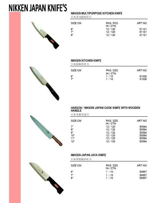
NIKKEN MULTIPURPOSE KITCHEN KNIFE日本多功能厨房刀SIZE CM PKG. PCS ART NOIN / CTN6” 12 / 120 51121 7” 12 / 120 51121 8” 12 / 120 51121 NIKKEN KITCHEN KNIFE日本胶柄爪哇刀SIZE CM PKG. DZS ART NOIN / CTN6” 1 / 10 51026 7” 1 / 10 51026 HAKKOH / NIKKEN JAPAN COOK KNIFE WITH WOODEN HANDLE日本木柄尖尾刀SIZE CM PKG. DZS ART NOIN / CTN7” 12 / 120 50594 8” 12 / 120 50594 9” 12 / 120 50594 10” 12 / 120 50594 11” 12 / 120 50594 12” 12 / 120 50594 NIKKEN JAPAN JAVA KNIFE日本黑胶柄爪哇刀SIZE CM PKG. DZS ART NOIN / CTN6” 1 / 10 50857 7” 1 / 10 50857 8” 1 / 10 50857JAPAN S/S JAVA KNIFE日本黑胶柄爪哇刀SIZE CM PKG. DZS ART NOIN / CTN5” - / 10 50509-56” - / 10 50509-67” - / 10 50509-7NIKKEN DURIAN KNIFE日本木柄榴连刀SIZE CM PKG. DZS ART NOIN / CTN4” 1 / 10 50734JAPAN CAMPING KNIFE 日本露营刀SIZE CM PKG. PCS ART NOIN/CTN 11.5” 6 / 60 LH-080012 FUNCTION HUNTING KNIFE十二功能猎刀SIZE CM PKG. PCS ART NOIN / CTN12 / 60 HK940NIKKEN JAPAN S/S WOODEN HANDLE CHOPPER日本木柄骨刀SIZE CM PKG. PCS ART NO IN/CTN 7” - / 60 50820NIKKEN JAPAN S/S PLASTIC HANDLE CHOPPERNIKKEN牌日本胶柄骨刀SIZE CM PKG. PCS ART NO IN/CTN 7” 1 / 60 50963 8” 1 / 60 50963NIKKEN JAPAN S/S CHINESE CHOPPER日本不锈钢菜刀SIZE CM PKG. PCS ART NO IN/CTN 7” 6 / 60 51308 8” 6 / 60 51308NIKKEN JAPAN S/S HAM SLICER WITH WOODEN HANDLE (STRAIGHT)日本木柄面包刀SIZE CM PKG. DZS ART NOIN / CTN10” 1 / 10 50957 12” 1 / 10 50957 14” 1 / 10 50957NIKKEN S/S DBL BLADE HAM SLICER日本胶柄面包刀SIZE CM PKG. DZS ART NOIN / CTN8” - / 20 51225 NIKKEN JAPAN HAM SLICER WITH SERRATION & WOODEN HANDLE日本有齿木柄面包刀SIZE CM PKG. DZS ART NO IN/CTN 10” 1 / 10 S491W 12” 1 / 10 S491W 14” 1 / 10 S491WNIKKEN S/S HAM SLICER日本木柄面包刀SIZE CM PKG. PCS ART NOIN / CTN10” 1 / 10 S491 12” 1 / 10 S491 14” 1 / 10 S491JAPAN PLASTIC HANDLE PEELER日本胶柄果子插心器SIZE CM PKG. PCS ART NOIN / CTN17.5 24 / 600 V1201JAPAN PARING KNIFE日本削皮刀SIZE CM PKG. PCS ART NOIN / CTN3.5” 12 / 600 23JAPAN WOODEN COVER FRUIT KNIFE日本介装果子刀SIZE CM PKG. DZS ART NOIN / CTN4” 1 / 50 50628JAPAN PLASTIC GRATER日本胶多功能菜头抽SIZE CM PKG. SETS ART NOIN / CTN22 x 8 20 / 200 0328-170JAPAN S/S CHEESE GRATER日本钢奶酪刨SIZE CM PKG. PCS ART NOIN / CTN23 - / 35 50341JAPAN S/S LEMON GRATER日本钢柠檬削皮器(丝条状)SIZE CM PKG. PCS ART NOIN / CTN14 - / 100 51112JAPAN GRATER日本剥皮器SIZE CM PKG. PCS ART NO IN/CTN 13.5 x 9 12 / 240 JPG-1BENRINER JAPAN VEGETABLE SLICER日本鱼生刨SIZE CM PKG. SETS ART NOIN / CTN31 x 9 - / 36 100815JAPAN 2 IN 1 FRUIT CRAVE日本2合1雕果刀匙SIZE CM PKG. PCS ART NOIN / CTN19” 10 / 120 0736-053NIKKEN PLASTIC HANDLE PEELER日本胶柄剥皮器SIZE CM PKG. PCS ART NO IN/CTN12 / 120 45248JAPAN S/S PIZZA CUTTER日本钢薄饼辘SIZE CM PKG. PCS ART NOIN / CTN15 - / 50 51105 JAPAN STAINLESS STEEL PIZZA CUTTER日本钢薄饼辘SIZE CM PKG. PCS ART NOIN / CTN19” 24 / 288 33SUN TIGER JAPAN SHARPENING STONE日本大块油石SIZE CM PKG. PCSART NO L x W x H IN / CTN8 x 3 x 2 1 / 15ST-320SUN TIGER JAPAN SHARPENING STONE日本大块油石SIZE CM PKG. PCSART NO L x W x H IN / CTN20.5 x 7.5 x 5 21 / 116JAPAN SHARPENING STONE日本大块油石SIZE CM PKG. PCSART NO L x W x H IN / CTN20.5 x 6.6 x 3.4 1 / 30800SIZE CM PKG. PCSART NO L x W x H IN / CTN20.7 x 7 x 6 1 / 301000SIZE CM PKG. PCS ART NO L x W x H IN / CTN20.9 x 7 x 6 1 / 18 1200JAPAN KNIFE SHARPENER日本磨刀器SIZE CM PKG. PCS ART NOIN / CTN16.5 - / 60 CT-19JAPAN STAINLESS STEEL PEELER日本不锈钢疏菜刨SIZE CM PKG. PCS ART NOIN / CTN9 x 17.5 - / 120 5-02-02NIKKEN JAPAN SUPPORTER SCISSOR—RED COLOUR日本高级厨房剪SIZE CM PKG. PCS ART NOIN / CTN10” 12 / 120 76364NIKKEN JAPAN SUPPORTER SCISSOR-BLUE日本高级厨房剪SIZE CM PKG. PCS ART NOIN / CTN10” 12 / 120 76306NIKKEN JAPAN SUPPORTER SCISSOR日本厨房剪SIZE CM PKG. PCS ART NOIN/CTN 9” 12 / 120 75893NIKKEN JAPAN SUPPORTER SCISSOR日本厨房剪SIZE CM PKG. PCS ART NOIN / CTN9.5” - / 120 75835NIKKEN JAPAN KITCHEN SCISSOR日本厨房剪SIZE CM PKG. PCS ART NOIN / CTN8” 12 / 120 KP-1500ACECHO JAPAN ICE CHISELECHO 牌日本冰插SIZE CM PKG. PCS ART NOIN/CTN 21” 12 / 120 0347-107CHICKEN SCISSOR-BLACK COLOUR 鸡骨剪(3.0mm)黑色SIZE CM PKG. PCS ART NOIN / CTN9.5” 12 / 72 YK0075NIKKEN JAPAN MULTI PURPOSE KITCHEN SCISSOR日本万能剪刀SIZE CM PKG. PCS ART NOIN/CTN 7” 12 / 120 75750R。
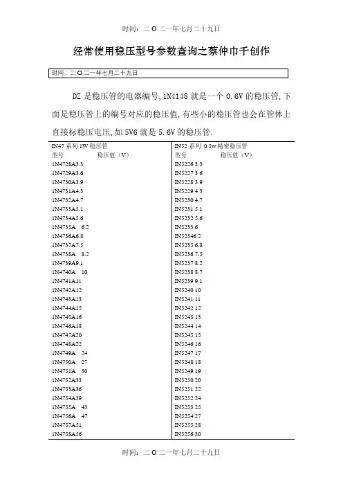
经常使用稳压型号参数查询之蔡仲巾千创作DZ是稳压管的电器编号,1N4148就是一个0.6V的稳压管,下面是稳压管上的编号对应的稳压值,有些小的稳压管也会在管体上直接标稳压电压,如5V6就是5.6V的稳压管.美标稳压二极管型号:HITACHI(日立):HITACHI(日立)0.5W稳压二极管型号参数稳压HZ3A1 2.5~2.7VHZ3A2 2.6~2.8VHZ3A3 2.6~2.9VHZ3B1 2.8~3.0VHZ3B2 2.9~3.1VHZ3B3 3.0~3.2V线性稳压器件(输入输出电流相等,压降3V以上)型号稳压(V) 最年夜输出电流可替代型号79L05 -5V 100mA79L06 -6V 100mA79L08 -8V 100mALM7805 5V 1A L7805,LM340T5LM7806 6V 1A L7806LM7808 8V 1A L7808LM7809 9V 1A L7809LM7812 12V 1A L7812,LM340T12LM7815 15V 1A L7815,LM340T15LM7818 18V 1A L7815LM7824 24V 1A L7824LM7905 -5V 1A L7905LM7906 -6V 1A L7906,KA7906LM7908 -8V 1A L7908LM7909 -9V 1A L7909LM7912 -12V 1A L7912LM7915 -15V 1A L7915LM7918 -18V 1A L7918LM7924 -24V 1A L792478L05 5V 100mA78L06 6V 100mA78L08 8V 100ma78L09 9V 100ma78L12 12V 100ma78L15 15V 100ma78L18 18V 100ma78L24 24V 100ma开关稳压器件(电压转换效率高)型号说明最年夜输出电流LM1575T-3.3 3.3V简易开关电源稳压器1ALM1575T-5.0 5V简易开关电源稳压器1ALM1575T-12 12V简易开关电源稳压器1ALM1575T-15 15V简易开关电源稳压器1ALM1575T-ADJ 简易开关电源稳压器(可调1.23V~37V) 1ALM1575HVT-3.3 3.3V简易开关电源稳压器1ALM1575HVT-5.0 5V简易开关电源稳压器1ALM1575HVT-12 12V简易开关电源稳压器1ALM1575HVT-15 15V简易开关电源稳压器1ALM1575HVT-ADJ 简易开关电源稳压器(可调1.23V~37V) 1ALM2575T-3.3 3.3V简易开关电源稳压器1ALM2575T-5.0 5V简易开关电源稳压器1ALM2575T-12 12V简易开关电源稳压器1ALM2575T-15 15V简易开关电源稳压器1ALM2575T-ADJ 简易开关电源稳压器(可调1.23V~ 37V) 1ALM2575HVT-3.3 3.3V简易开关电源稳压器1ALM2575HVT-5.0 5V简易开关电源稳压器1ALM2575HVT-12 12V简易开关电源稳压器1ALM2575HVT-15 15V简易开关电源稳压器1ALM2575HVT-ADJ 简易开关电源稳压器(可调1.23V~37V) 1ALM2576T-3.3 3.3V简易开关电源稳压器3ALM2576T-5.0 5.0V简易开关电源稳压器3ALM2576T-12 12V简易开关电源稳压器3ALM2576T-15 15V简易开关电源稳压器3ALM2576T-ADJ 简易开关电源稳压器(可调1.23V~37V) 3ALM2576HVT-3.3 3.3V简易开关电源稳压器3ALM2576HVT-5.0 5.0V简易开关电源稳压器3ALM2576HVT-12 12V简易开关电源稳压器3ALM2576HVT-15 15V简易开关电源稳压器3ALM2576HVT-ADJ 简易开关电源稳压器(可调1.23V~37V) 3A。
47nf安规电容
摘要:
1.47nf 安规电容的概述
2.47nf 安规电容的特点
3.47nf 安规电容的应用领域
4.47nf 安规电容的选购与使用注意事项
正文:
一、47nf 安规电容的概述
47nf 安规电容,全称为47 纳法拉的安规电容,是一种常见的电容器件。
它的主要作用是在电路中进行滤波、去耦、旁路等,以保证电路的稳定性和安全性。
二、47nf 安规电容的特点
1.容量:47nf 安规电容的容量为47 纳法拉,属于较小的电容容量范围。
2.安规:47nf 安规电容符合我国的安规标准,具有较好的安全性能。
3.稳定性:47nf 安规电容具有较好的稳定性,可以在高温、高压等环境下保持稳定的工作性能。
三、47nf 安规电容的应用领域
47nf 安规电容广泛应用于各种电子设备和电路中,如电源、电视机、收音机、计算机等,主要用于滤波、去耦、旁路等。
四、47nf 安规电容的选购与使用注意事项
1.选购:在选购47nf 安规电容时,应选择正规厂家生产的产品,并查看产品的安规认证标志。
2.使用:在使用47nf 安规电容时,应注意以下几点:
(1)正确安装:根据电路图,正确安装电容,避免错位或反接。
(2)注意电容的工作电压和电流:选择电容时,应确保其工作电压和电流符合电路的要求。
(3)保持良好的散热:电容器在工作过程中会产生热量,应确保电容器周围有良好的散热环境,以保证电容器的安全使用。
总之,47nf 安规电容是一种重要的电子元器件,广泛应用于各种电子设备和电路中。
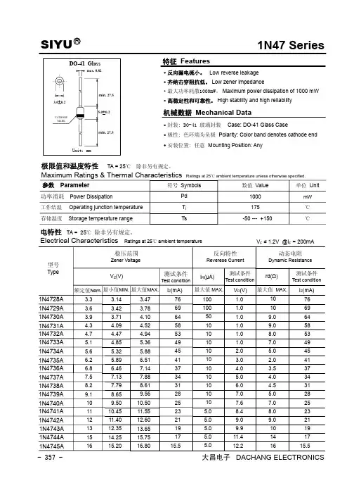
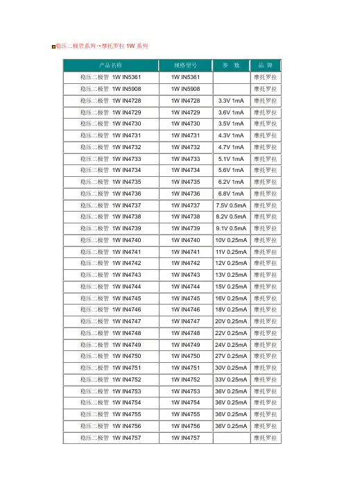
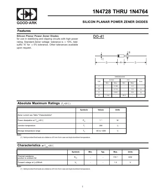
稳压二极管系列→摩托罗拉1W系列产品名称规格型号参数品牌稳压二极管1W IN53611W IN5361摩托罗拉稳压二极管1W IN59081W IN5908摩托罗拉稳压二极管1W IN47281W IN4728 3.3V 1mA摩托罗拉稳压二极管1W IN47291W IN4729 3.6V 1mA摩托罗拉稳压二极管1W IN47301W IN4730 3.5V 1mA摩托罗拉稳压二极管1W IN47311W IN4731 4.3V 1mA摩托罗拉稳压二极管1W IN47321W IN4732 4.7V 1mA摩托罗拉稳压二极管1W IN47331W IN4733 5.1V 1mA摩托罗拉稳压二极管1W IN47341W IN4734 5.6V 1mA摩托罗拉稳压二极管1W IN47351W IN4735 6.2V 1mA摩托罗拉稳压二极管1W IN47361W IN4736 6.8V 1mA摩托罗拉稳压二极管1W IN47371W IN47377.5V 0.5mA摩托罗拉稳压二极管1W IN47381W IN47388.2V 0.5mA摩托罗拉稳压二极管1W IN47391W IN47399.1V 0.5mA摩托罗拉稳压二极管1W IN47401W IN474010V 0.25mA摩托罗拉稳压二极管1W IN47411W IN474111V 0.25mA摩托罗拉稳压二极管1W IN47421W IN474212V 0.25mA摩托罗拉稳压二极管1W IN47431W IN474313V 0.25mA摩托罗拉稳压二极管1W IN47441W IN474415V 0.25mA摩托罗拉稳压二极管1W IN47451W IN474516V 0.25mA摩托罗拉稳压二极管1W IN47461W IN474618V 0.25mA摩托罗拉稳压二极管1W IN47471W IN474720V 0.25mA摩托罗拉稳压二极管1W IN47481W IN474822V 0.25mA摩托罗拉稳压二极管1W IN47491W IN474924V 0.25mA摩托罗拉稳压二极管1W IN47501W IN475027V 0.25mA摩托罗拉稳压二极管1W IN47511W IN475130V 0.25mA摩托罗拉稳压二极管1W IN47521W IN475233V 0.25mA摩托罗拉稳压二极管1W IN47531W IN475336V 0.25mA摩托罗拉稳压二极管1W IN47541W IN475436V 0.25mA摩托罗拉稳压二极管1W IN47551W IN475536V 0.25mA摩托罗拉稳压二极管1W IN47561W IN475636V 0.25mA摩托罗拉稳压二极管1W IN47571W IN4757摩托罗拉。
亚什兰压敏胶参数-概述说明以及解释1.引言1.1 概述概述部分的内容可以按照如下方式编写:引言部分是文章的开场白,对文章进行一个全面而简要的介绍。
在本文中,我们将重点关注亚什兰压敏胶的参数。
亚什兰压敏胶作为一种特殊类型的胶黏剂,在许多工业和科学领域中得到广泛应用。
其独特的物理和化学性质使得亚什兰压敏胶在粘合和密封应用中具有出色的性能。
本文将围绕亚什兰压敏胶的定义和特点、应用领域以及其参数及其影响因素展开讨论。
首先,我们将对亚什兰压敏胶的定义和特点进行详细介绍,包括其胶黏性、柔韧性和耐久性等方面的特点。
其次,我们将探讨亚什兰压敏胶的应用领域,包括医疗、电子、汽车和航空等领域,以展示其广泛的用途和潜力。
然后,我们将重点关注亚什兰压敏胶的参数及其影响因素。
亚什兰压敏胶的参数包括黏度、粘接强度、剥离强度等,这些参数直接影响着胶黏剂的性能和质量。
我们将深入研究这些参数的测量方法和影响因素,包括温度、含水量和压力等因素的影响。
最后,我们将对亚什兰压敏胶的参数进行总结,提供实际应用建议和评价。
同时,我们也将展望亚什兰压敏胶参数研究的未来发展方向,以期能够进一步提高胶黏剂的性能和优化应用效果。
通过对亚什兰压敏胶的参数进行深入研究,我们有望为胶黏剂领域的科学家、工程师和制造商们提供有价值的参考和指导,推动该领域的进一步发展。
同时,对于广大读者,对亚什兰压敏胶参数的了解也将有助于他们更好地理解胶黏剂在日常生活中的应用和价值。
1.2 文章结构本文将从三个方面介绍亚什兰压敏胶的参数。
首先,在引言部分概述了本文的目的和重要性。
接下来,在正文部分,将详细阐述亚什兰压敏胶的定义和特点,以及其在不同领域的应用。
最后,在结论部分,总结了亚什兰压敏胶的重要参数,并对其进行了分析和评价。
同时,还展望了亚什兰压敏胶参数的未来研究方向。
通过这样的结构安排,读者将能全面了解亚什兰压敏胶的参数及其影响因素,以及其在实际应用中的潜力和发展趋势。
镍铁锰酸钠真密度铜铁锰酸钠
【原创版】
目录
1.镍铁锰酸钠的概述
2.镍铁锰酸钠的真密度
3.铜铁锰酸钠的概述
4.铜铁锰酸钠与镍铁锰酸钠的比较
正文
1.镍铁锰酸钠的概述
镍铁锰酸钠(NaMnFeO4)是一种常见的锂离子电池正极材料,具有良好的电化学性能和高容量。
它是由镍、铁、锰和氧四种元素组成的复合氧化物,具有橄榄石型结构。
在锂离子电池领域,镍铁锰酸钠作为一种环保、高性能的正极材料得到了广泛的应用。
2.镍铁锰酸钠的真密度
镍铁锰酸钠的真密度是指在 20 摄氏度、101kPa 条件下,单位体积内物质的质量。
镍铁锰酸钠的真密度一般在 5.2-5.4 g/cm之间,这个范围内的真密度可以保证镍铁锰酸钠在电池充放电过程中具有良好的体积稳定性。
3.铜铁锰酸钠的概述
铜铁锰酸钠(NaMnFeO4)是一种锂离子电池正极材料,与镍铁锰酸钠类似,它也是由镍、铁、锰和氧四种元素组成的复合氧化物,具有橄榄石型结构。
铜铁锰酸钠具有较高的容量、良好的循环性能和环境友好性,因此在锂离子电池领域也具有一定的应用前景。
4.铜铁锰酸钠与镍铁锰酸钠的比较
虽然铜铁锰酸钠和镍铁锰酸钠具有相似的结构和性能,但它们在锂离子电池应用中仍有一些差异。
相比镍铁锰酸钠,铜铁锰酸钠具有更高的容量,可以实现更高的能量密度。
然而,铜铁锰酸钠的循环性能和稳定性相对较差,这限制了其在锂离子电池领域的应用。
耐驰螺杆泵政府政策和产业优势,积极保障展会的前瞻性和引领性,面向全球发布展会信息。
大会预设展位9个,预计展出面积7平方米,邀请专业观众45人次,重点加强专业观众和国外采购商的组织邀请工作。
激情亚运,和谐亚洲,中国国际泵阀展在亚运会与残运会之间举办,充分利用了两会带来的巨大商机!展会得到了美国、德国、日本、新加坡、越南等国家与地区的商会、协会与贸易机构的大力支持,积极组织境外企业参展或参观采购;CPVPE2将是世界资源共享的流体技【耐驰螺杆泵】产品简介:G型单螺杆泵,它的最大特点是对介质的适应性强、流量平稳、压力脉动动小、自吸能力高,这是其它任何泵种所不能替代的。
,压力为0.6~1.2MPa,特殊要求压力可达3MPa,可满足广大用户对单螺杆泵的不同需求。
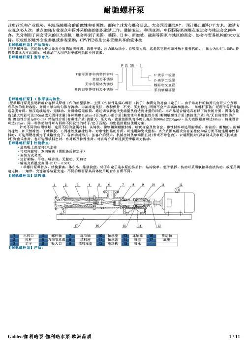
【耐驰螺杆泵】型号意义:【耐驰螺杆泵】工作原理与特性:G型单螺杆泵是按迥转啮合容积式原理工作的新型泵种。
主要工作部件是偏心螺杆(转子)和固定的衬套(定子)。
由于该部件的特殊几何开头分别形成单独的密封容腔。
介质由轴向均匀推行流动。
内部流速代低,容积保持 不变。
压力稳定,因而不会产品涡流和搅动。
单螺杆泵被广泛用于各行业输送各类介质,恒压连续运行,无脉动,介质输送无破损,通过调节转速改变流量从而达到计量的目的。
本产品适合输送具有以下特性的介质:固体含量高(最大粒径可达150mm)或无固体含量|各种粘度(1mPas-3百万mPas)的介质|触变性和易膨胀性介质|剪切敏感性介质|磨蚀性介质|有/无自润滑性的介质|腐蚀性介质(pH=O-14)|粘结性介质|有毒性介质|流量大、压力高·流量范围从每小时几毫升到500m3(2200gpm)·压力范围最高可达48bar,特殊设计可达72bar。
同一种传动部件可与四种不同设计的转子/定子匹配,为您提供最佳使用方案。
针对不同的应用领域,选用不同的金属材料,从铸铁、镍铬钢到耐酸材料、哈氏合金及钛合金。
Neon™ Transfection SystemFor transfecting mammalian cells, including primary and stem cells, with high transfection efficiency. Catalog Numbers MPK5000, MPK1025, MPK1096, MPK10025, MPK10096Doc. Part No. 25-1056 Pub. No. MAN0001632 Rev.B.0WARNING! For safety and biohazard guidelines, see the “Safety” appendix in the Neon™ Transfection System User Guide (Pub.No. MAN0001557). Read the Safety Data Sheets (SDSs) and follow the handling instructions. Wear appropriate protective eyewear, clothing, and gloves.Note: This Quick Reference is intended as a benchtop reference for experienced users of the Neon™ Transfection System User Guide (Pub. No. MAN0001557). For detailed instructions, supplemental procedures, and troubleshooting, see the Neon™ Transfection System User Guide (Pub. No. MAN0001557).General guidelines•Prepare high-quality plasmid DNA at a concentration of 1 to 5 μg/μL in deionized water or TE buffer, or high quality RNAi duplex at a concentration of 100–250 μM in nuclease-free water.•Use an appropriate GFP (green fluorescent protein) construct or siRNA control to determine transfection efficiency. See the Neon™Transfection System User Guide (Pub. No. MAN0001557) for details.•Use Resuspension Buffer R for established adherent and suspension cells, as well as primary adherent cells. Use Resuspension Buffer T with high voltage protocols of 1900 V or more. If arcing occurs with Resuspension Buffer R, consider switching toResuspension Buffer T.•Based on your initial results, you may need to optimize the electroporation parameters for your experiment using an 18-well or pre-programmed 24-well optimization protocol.•Discard the Neon™ Tips after 2 usages and Neon™ Tubes after 10 usages as a biological hazard. Change the tube and buffer when switching to a different plasmid DNA/siRNA or cell type.•The volume of plasmid DNA or siRNA added to the tranfection reaction should not exceed 10% of the total transfection volume.•Visit for a library of electroporation protocols for a variety of commonly used cell types.Prepare cellsFor the appropriate volume of medium to use based on cell density, or plating volumes for other plate formats, see “Amount of reagents” on page 2.1.Cultivate the required number of cells (70% to 90%confluent on the day of transfection) by seeding a flaskcontaining fresh growth medium 1 to 2 days prior toeletroporation.2.On the day of the experiment, pre-warm aliquots of culturemedium containing serum, PBS (without Ca2+and Mg2+), and Trypsin/EDTA solution to 37°C.3.Rinse the cells with PBS (without Ca2+and Mg2+), thentrypsinize the cells with the Trypsin/EDTA solution.4.Take an aliquot of trypsinized cell suspension, then countcells to determine the cell density.5.Harvest the cells in growth medium containing serum.6.Transfer cells to a 1.5-mL microcentrifuge tube or a 15-mLconical tube, then centrifuge the cells at 100 - 400 × g for 5 minutes at room temperature.7.Wash cells with PBS (without Ca2+and Mg2+) bycentrifugation at 100 - 400 × g for 5 minutes at roomtemperature.8.Aspirate the PBS, then resupsend the cell pellet inResuspension Buffer R (or Resuspension Buffer T forprograms ≥ 1900 V) at a final density of 1.0 × 10⁷ cells/mL for adherent cells or 2.0 × 10⁷ cells/ml for suspension cells.Gently pipette the cells to obtain a single cell suspension.IMPORTANT! Avoid storing the cell suspension for more than 15 to 30 minutes at room temperature. This will reduce cell viability and transfection efficiency.9.Prepare 24-well plates by filling the wells with 500 μL ofculture medium containing serum and supplements, butwithout antibiotics. Pre-incubate plates in a 37°C, 5% CO2 humidified incubator.Amount of reagentsFor each electroporation sample, the amount of plasmid DNA/siRNA, cell number, and volume of plating medium per well are listed in the following table. Use Resuspension Buffer T for cell types that require high voltage protocols of 1900 V or more. For all other cell types, use Resuspension Buffer R.[1]Use Resuspension Buffer T for primary suspension blood cells.Using the Neon ™Transfection SystemFor details on setting up the Neon ™device and Neon ™PipetteStation, see the Neon ™Transfection System User Guide (Pub. No.MAN0001557).1.Select the appropriate protocol for your cell type. Use one ofthe following options:•Input the electroporation parameters in the Input window if you already have the electroporation parameters for your cell type.•Tap Database , then select the cell-specificelectroporation parameters that you have added for various cell types.•Tap Optimization to perform the optimization protocol for your cell type.2.Fill the Neon ™Tube with 3 mL of Electrolytic Buffer (useBuffer E for the 10 μL Neon ™Tip and Buffer E2 for the 100μL Neon ™Tip).Note: Make sure that the electrode on the side of the tube is completely immersed in buffer. 3.Insert the Neon ™ Tube into the Neon ™Pipette Station untilyou hear a click sound (Figure 1).Figure 1 Schematic of Neon ™ Tube and Neon ™ Pipette Station.4.Transfer the appropriate amount of plasmid DNA/siRNA intoa sterile, 1.5 mL microcentrifuge tube.5.Add cells to the tube containing plasmid DNA/siRNA, thengently mix. See “Amount of reagents” on page 2 for cell number, DNA/siRNA amount, and plating volumes to use.6.To insert a Neon ™Tip into the Neon ™Pipette, press thepush-button on the pipette to the second stop to open the clamp.7.Insert the top-head of the Neon ™Pipette into the Neon ™Tipuntil the clamp fully picks up the mount stem of the piston (Figure 2).Figure 2 Schematic of Neon ™ Pipette and Neon ™Tip.8.Gently release the push-button, continuing to apply adownward pressure on the pipette, ensuring that the tip is sealed onto the pipette without any gaps.9.Press the push-button on the Neon ™Pipette to the first stopand immerse the Neon ™Tip into the cell-DNA/siRNA mixture.Slowly release the push-button on the pipette to aspirate thecell-DNA/siRNA mixture into the Neon ™Tip (Figure 3).Figure 3 Schematic of Neon ™Tip.Note: Avoid air bubbles during pipetting as air bubbles cause arcing during electroporation leading to lowered or failed transfection. If you notice air bubbles in the tip,discard the sample, then carefully aspirate the fresh sample into the tip again without any air bubbles.10.Insert the Neon ™Pipette with the sample vertically into theNeon ™ Tube placed in the Neon ™Pipette Station until youhear a click sound (Figure 4).Figure 4 Schematic of Neon ™ Tube and Neon ™ Pipette Station.Note: Ensure that the metal head of the Neon ™pipette projection is inserted into the groove of the pipette station.11.Ensure that you have selected the appropriateelectroporation protocol, then press Start on the touchscreen.12.The Neon ™device automatically checks for the properinsertion of the Neon ™ Tube and Neon ™Pipette before delivering the electric pulse.13.After delivering the electric pulse, Complete is displayed onthe touchscreen to indicate that electroporation is complete.14.Slowly remove the Neon ™Pipette from the Neon ™PipetteStation. Immediately transfer the samples from the Neon ™Tip by pressing the push-button on the pipette to the first stop into the prepared culture plate containing prewarmed medium with serum and supplements but without antibiotics.Note: Discard the Neon ™ Tip into an appropriate biologicalhazardous waste container. To discard the Neon ™Tip, press the push-button to the second stop into an appropriate biological hazardous waste container.15.Repeat step 6 to step 14 for the remaining samples.Note: Be sure to change the Neon ™Tips after using it twiceand Neon ™ Tubes after 10 usages. Use a new Neon ™Tip andNeon ™Tube for each new plasmid DNA sample.16.Gently rock the plate to ensure even distribution of the cells.Incubate the plate at 37℃ in a humidified CO 2 incubator.17.If you are not using the Neon ™device, turn the power switchon the rear to OFF .18.Assay samples to determine the transfection efficiency(e.g., fluorescence microscopy or functional assay) or geneknockdown (for siRNA).19.Based on your initial results, you may need to optimizedthe electroporation parameters for your cell type. For more information, see the Neon™ Transfection System User Guide (Pub. No. MAN0001557).Life Technologies Corporation | 5781 Van Allen Way | Carlsbad, California 92008 USAFor descriptions of symbols on product labels or product documents, go to /symbols-definition.The information in this guide is subject to change without notice.DISCLAIMER: TO THE EXTENT ALLOWED BY LAW, THERMO FISHER SCIENTIFIC INC. AND/OR ITS AFFILIATE(S) WILL NOT BE LIABLE FOR SPECIAL, INCIDENTAL, INDIRECT, PUNITIVE, MULTIPLE, OR CONSEQUENTIAL DAMAGES IN CONNECTION WITH OR ARISING FROM THIS DOCUMENT, INCLUDING YOUR USE OF IT.Important Licensing Information: These products may be covered by one or more Limited Use Label Licenses. By use of these products, you accept the terms and conditions of all applicable Limited Use Label Licenses.©2021 Thermo Fisher Scientific Inc. All rights reserved. All trademarks are the property of Thermo Fisher Scientific and its subsidiaries unless otherwise specified./support | /askaquestion。
TOSHIBA Transistor Silicon NPN ·PNP Epitaxial Type(PCT Process) (Bias Resistor Built-in Transistor)RN47A2JESwitching, Inverter Circuit, Interface Circuit and Driver Circuit Applications• Two devices are incorporated into an Extreme-Super-Mini (5-pin)package.• Incorporating a bias resistor into a transistor reduces parts count.Reducing the parts count enables the manufacture of ever more compact equipment and lowers assembly cost.Equivalent Circuit and Bias Resistor ValuesQ1Q2R1: 22 k Ω (Q1, Q2 common) R2: 22 k Ω (Q1, Q2 common) Q1: RN1103F Q2: RN2103FMarking Equivalent Circuit (top view)Unit: mm1.EMITTER12.BASE13.EMITTER24.COLLECTOR25.COLLECTOR1 BASE2(E1)(B1) (E2) (C2) (C1) (B2)JEDEC― JEITA―TOSHIBA 2-2P1E Weight: 0.003g (typ.)BB2 2453 1 2Absolute Maximum Ratings (Ta = 25°C) (Q1)UnitRatingCharacteristics SymbolCollector-base voltage V CBO50 VCollector-emitter voltage V CEO50 VEmitter-base voltage V EBO10 VCollector current I C100 mAAbsolute Maximum Ratings (Ta = 25°C) (Q2)UnitRatingCharacteristics SymbolCollector-base voltage V CBO−50 VCollector-emitter voltage V CEO−50 VEmitter-base voltage V EBO−10 VCollector current I C−100 mAAbsolute Maximum Ratings (Ta = 25°C) (Q1, Q2 common)RatingUnitCharacteristics SymbolCollector power dissipation P C (Note 1)100 mW°CJunction temperature T j 150Storage temperature range T stg−55~150 °CNote: Using continuously under heavy loads (e.g. the application of high temperature/current/voltage and the significant change in temperature, etc.) may cause this product to decrease in the reliability significantlyeven if the operating conditions (i.e. operating temperature/current/voltage, etc.) are within the absolutemaximum ratings.Please design the appropriate reliability upon reviewing the Toshiba Semiconductor Reliability Handbook(“Handling Precautions”/“Derating Concept and Methods”) and individual reliability data (i.e. reliability testreport and estimated failure rate, etc).Note 1: Total ratingElectrical Characteristics (Ta = 25°C) (Q1)Max UnitTyp.Min Characteristics SymbolTestConditionI CBO V CB= 50 V, I E= 0 ⎯ ⎯ 100nA Collector cut-off currentI CEO V CE= 50 V, I B= 0 ⎯ ⎯ 500Emitter cut-off current I EBO V EB= 10 V, I C= 0 0.17 ⎯ 0.33mA DC current gain h FE V CE= 5 V, I C= 10 mA 70 ⎯ ⎯Collector-emitter saturation voltage V CE (sat)I C= 5 mA, I B= 0.25 mA ⎯ 0.1 0.3 V Input voltage (ON) V I (ON)V CE= 0.2 V, I C= 5 mA 1.3 ⎯ 3.0 V Input voltage (OFF) V I (OFF)V CE= 5 V, I C= 0.1 mA 1.0 ⎯ 1.5 V Transition frequency f T V CE= 10 V, I C= 5 mA ⎯ 250 ⎯ MHz Collector output capacitance C ob V CB= 10 V, I E= 0, f = 1 MHz ⎯ 3 ⎯ pF28.6kΩInput resistor R1 ⎯ 15.422Resistor ratio R1/R2 ⎯ 0.8 1.0 1.2 Electrical Characteristics (Ta = 25°C) (Q2)Typ.Max UnitMinConditionTestCharacteristics SymbolI CBO V CB=−50 V, I E= 0 ⎯ ⎯−100nA Collector cut-off currentI CEO V CE=−50 V, I B= 0 ⎯ ⎯ −500Emitter cut-off current I EBO V EB=−10 V, I C= 0 −0.17 ⎯ −0.33mA DC current gain h FE V CE=−5 V, I C=−10 mA 70 ⎯ ⎯Collector-emitter saturation voltage V CE (sat)I C=−5 mA, I B=−0.25 mA ⎯−0.1 −0.3V Input voltage (ON) V I (ON)V CE=−0.2 V, I C=−5 mA −1.3 ⎯−3.0V Input voltage (OFF) V I (OFF)V CE=−5 V, I C=−0.1 mA −1.0 ⎯−1.5V Transition frequency f T V CE=−10 V, I C=−5 mA ⎯ 200 ⎯ MHz Collector output capacitance C ob V CB=−10 V, I E= 0, f = 1 MHz ⎯ 3 ⎯ pF28.6kΩInput resistor R1 ⎯ 15.422Resistor ratio R1/R2 ⎯ 0.8 1.0 1.2(μA )Q1, Q2 CommonAMBIENT TEMPERATURE Ta (°C) P C* – TaC O L L E C T O R P O W E RD I S S I P A T I O N P C (m W )0 175125 15075 100 075251005012525 50 *Total Rating.RESTRICTIONS ON PRODUCT USE20070701-EN GENERAL •The information contained herein is subject to change without notice.•TOSHIBA is continually working to improve the quality and reliability of its products. Nevertheless, semiconductor devices in general can malfunction or fail due to their inherent electrical sensitivity and vulnerability to physical stress. It is the responsibility of the buyer, when utilizing TOSHIBA products, to comply with the standards of safety in making a safe design for the entire system, and to avoid situations in which a malfunction or failure of such TOSHIBA products could cause loss of human life, bodily injury or damage to property.In developing your designs, please ensure that TOSHIBA products are used within specified operating ranges as set forth in the most recent TOSHIBA products specifications. Also, please keep in mind the precautions and conditions set forth in the “Handling Guide for Semiconductor Devices,” or “TOSHIBA Semiconductor Reliability Handbook” etc.• The TOSHIBA products listed in this document are intended for usage in general electronics applications (computer, personal equipment, office equipment, measuring equipment, industrial robotics, domestic appliances, etc.).These TOSHIBA products are neither intended nor warranted for usage in equipment that requires extraordinarily high quality and/or reliability or a malfunction or failure of which may cause loss of human life or bodily injury (“Unintended Usage”). Unintended Usage include atomic energy control instruments, airplane or spaceship instruments, transportation instruments, traffic signal instruments, combustion control instruments, medical instruments, all types of safety devices, etc.. Unintended Usage of TOSHIBA products listed in his document shall be made at the customer’s own risk.•The products described in this document shall not be used or embedded to any downstream products of which manufacture, use and/or sale are prohibited under any applicable laws and regulations.• The information contained herein is presented only as a guide for the applications of our products. No responsibility is assumed by TOSHIBA for any infringements of patents or other rights of the third parties which may result from its use. No license is granted by implication or otherwise under any patents or other rights of TOSHIBA or the third parties.• Please contact your sales representative for product-by-product details in this document regarding RoHS compatibility. Please use these products in this document in compliance with all applicable laws and regulations that regulate the inclusion or use of controlled substances. Toshiba assumes no liability for damage or losses occurring as a result of noncompliance with applicable laws and regulations.。
47nf电容标号
47nf电容标号指的是一个电容器的标识,其中“47nf”表示该电容器的容量为47纳法拉(nanofarad),“n”表示纳,是10的负9次方,因此47nf 也写作47nF。
电容器是一种储能元件,通常由两个导体之间的绝缘材料构成,可以存储电荷。
在电子电路中,电容器常被用于滤波、耦合、去耦、谐振等应用。
电容器的容量是衡量其存储电荷能力的重要参数,单位是法拉(F),而纳法拉是法拉的千分之一,是微小电容的常用单位。
在电路设计中,电容器的容量大小通常需要考虑电路的工作频率、电压、电流等参数。
除了容量之外,电容器还有其他一些重要参数,如耐压(最大允许工作电压)、介质类型(绝缘材料类型)、温度系数等。
在选择电容器时,需要根据具体的应用场景和电路要求综合考虑这些参数。
总之,47nf电容标号指的是一个容量为47纳法拉的电容器,它是电子电路中常用的一种元件,用于多种应用。
在选择和使用电容器时,需要考虑其容量、耐压、介质类型等参数,以确保电路的正常工作。
钽电容耐压值的表示方法钽电容上面标着106F表示: 106是容量为10UfF应是耐压值为2.5V钽电容耐压用不同的字母来标注,如下:F: 2.5G: 4L、J: 6.3A: 10C: 16D: 20E:25V:35T:50在体积一定的情况下,容值越大,耐压值越小。
目前全球主要有以下几个品牌的钽电容:AVX、KEMET、VISHAY、NEC、NICHICON。
市场上的钽电容,分为黄钽和黑钽两种。
黄钽品牌主要是:AVX KEMET 黑钽主要品牌是:NEC、NICHICON。
市场占有方面:AVX远高于KEMET,NEC高于NICHICON。
现在市场上的钽电价格变化比较大。
AVX涨价20%--30% , KEMET涨价15%-20%,NEC涨价10%--20%。
涨价的主要原因个人认为有这么几个原因:1.市场上原料钽价格上涨 2.劳动力成本的增加。
另外可能有朋友要问黄钽与黑钽的区别。
简单来说,黑钽是开模将钽粉压成型,而黄钽,是在表面用聚氧树脂包裹而成。
由于生产工艺的原因,黑钽的部空间没有得到最有效的利用,所以黄钽能做的容量会比黑钽要大,也就是说有些黄钽能做到的规格型号,黑钽做不了。
另外,前面有朋友说到Polymer,Polymer现在主要是 AVX与KEMET在做。
Polymer与比普通的二氧化锰的优势在于:普通的钽电他的实际使用电压一般是50%,Polymer一般在80%以上。
举个例子来说:100uf 10v的普通电容,在实际使用的时候,额定电压不能超过5V,如果使用Polymer材料的电容,那么只需要100uf 6.3v的。
但由于价格问题,Polymer现在在普通的电子产品上用的不是很多。
我所知道的,在笔记本电脑上有些有用到。
AVX与KEMET的优劣:AVX在军用,民用市场上的占有量都很大,在普通电容的市场上,AVX无论品质还是市场占有量都远强与KEMET。
价格上,AVX比KEMET 更贵。
KEMET他主要问题是其电容的耐压值不够,举例说:100uf 10v的电容,测试的电压按道理应该能达到5V,但若真用5V电压去测试的话,很可能会击穿。