TSOP39238中文资料
- 格式:pdf
- 大小:158.17 KB
- 文档页数:8

UC3843中文资料1. 简介UC3843是一款集成了PWM控制电路的高性能电源管理芯片。
它能够通过自身的内部反馈环路来实现稳定的输出电压,并且可调节输出电压范围。
这使得UC3843非常适用于开关电源和DC-DC转换应用中。
UC3843具有低启动电流、内部锁死和内部软启动功能,能够有效地降低功耗和延长系统寿命。
此外,它还具有短路保护、过温保护和欠压保护功能,确保了系统的安全性和可靠性。
2. 特点•集成了PWM控制电路,适用于开关电源和DC-DC转换应用。
•可调节的输出电压范围,能够满足不同应用的需求。
•低启动电流,节省功耗,提高系统效率。
•内部锁死和软启动功能,保护系统并延长使用寿命。
•短路保护、过温保护和欠压保护功能,确保系统安全可靠。
3. 参数规格以下是UC3843的主要参数规格:•输入电压范围:5V至25V•输出电压范围:0V至24V•最大输出电流:1A•工作频率:50kHz至500kHz•工作温度范围:-40°C至125°C•封装:DIP-8、SOP-84. 应用示例UC3843广泛应用于各种开关电源和DC-DC转换器设计中。
以下是一些应用示例:4.1 5V至12V降压转换器UC3843可以用于设计一个从5V输入降压到12V输出的DC-DC转换器。
通过调节内部反馈环路,可以使输出电压保持稳定在12V。
此外,UC3843的低启动电流和软启动功能确保了系统的正常启动和运行。
4.2 24V恒流LED驱动器UC3843还可以用于设计一个24V恒流LED驱动器。
通过控制PWM信号的占空比,可以调节LED的亮度,并通过反馈电路实现恒流驱动。
短路保护和过温保护功能能够保护LED和驱动器的安全性。
4.3 太阳能充电控制器由于UC3843具有广泛的输入电压范围和可调节的输出电压范围,因此非常适合用于设计太阳能充电控制器。
通过控制PWM信号,可以实现对充电电流的精确控制,并通过反馈电路实现恒压和恒流充电。


IR Receiver Modules for Remote Control SystemsTSOP382.., TSOP384.. Vishay SemiconductorsMECHANICAL DATA Pinning:1 = OUT,2 = GND,3 = V S FEATURES•Very low supply current•Photo detector and preamplifier in one package •Internal filter for PCM frequency•Improved shielding against EMI•Supply voltage: 2.5 V to 5.5 V•Improved immunity against ambient light•Insensitive to supply voltage ripple and noise •Component in accordance to RoH S 2002/95/EC and WEEE 2002/96/ECDESCRIPTIONThe TSOP382.., TSOP384.. series are miniaturized receivers for infrared remote control systems. A PIN diode and a preamplifier are assembled on a lead frame, the epoxy package acts as an IR filter.The demodulated output signal can be directly decoded by a microprocessor. The TSOP382.. is compatible with all common IR remote control data formats. The TSOP384.. is optimized to suppress almost all spurious pulses from energy saving fluorescent lamps but will also suppress some data signals.This component has not been qualified according to automotive specifications.BLOCK DIAGRAM APPLICATION CIRCUIT19026PARTS TABLECARRIER FREQUENCY STANDARD APPLICATIONS (AGC2/AGC8)VERY NOISY ENVIRONMENTS (AGC4) 30 kHz TSOP38230TSOP3843033 kHz TSOP38233TSOP3843336 kHz TSOP38236TSOP3843638 kHz TSOP38238TSOP3843840 kHz TSOP38240TSOP3844056 kHz TSOP38256TSOP38456TSOP382.., TSOP384..IR Receiver Modules for Remote Control SystemsVishay SemiconductorsNote(1)Stresses beyond those listed under “Absolute Maximum Ratings” may cause permanent damage to the device. This is a stress rating only and functional operation of the device at these or any other conditions beyond those indicated in the operational sections of this specification is not implied. Exposure to absolute maximum rating condtions for extended periods may affect the device reliability.Note (1)T amb = 25°C, unless otherwise specifiedTYPICAL CHARACTERISTICST amb = 25°C, unless otherwise specifiedFig. 1 - Output Active LowFig. 2 - Pulse Length and Sensitivity in Dark AmbientABSOLUTE MAXIMUM RATINGS (1)PARAMETER TEST CONDITIONSYMBOLVALUE UNIT Supply voltage (pin 3)V S - 0.3 to + 6.0V Supply current (pin 3)I S 3mA Output voltage (pin 1)V O - 0.3 to (V S + 0.3)V Output current (pin 1)I O 5mA Junction temperatureT j 100°C Storage temperature range T stg - 25 to + 85°C Operating temperature range T amb - 25 to + 85°C Power consumption T amb ≤ 85°C P tot 10mW Soldering temperaturet ≤ 10 s, 1 mm from case T sd260°CELECTRICAL AND OPTICAL CHARACTERISTICS (1)PARAMETER TEST CONDITION SYMBOL MIN.TYP.MAX.UNIT Supply current (pin 3)E v = 0, V S = 3.3 V I SD 0.270.350.45mA E v = 40 klx, sunlightI SH 0.45mA Supply voltage V S 2.55.5V Transmission distance E v = 0, test signal see fig. 1,IR diode TSAL6200,I F = 250 mA d 45m Output voltage low (pin 1)I OSL = 0.5 mA, E e = 0.7 mW/m 2,test signal see fig. 1V OSL 100mV Minimum irradiance Pulse width tolerance:t pi - 5/f o < t po < t pi + 6/f o ,test signal see fig. 1E e min.0.150.35mW/m 2Maximum irradiance t pi - 5/f o < t po < t pi + 6/f o ,test signal see fig. 1E e max.30W/m 2DirectivityAngle of half transmission distanceϕ1/2± 45degE eV O V VTSOP382.., TSOP384..Vishay SemiconductorsIR Receiver Modules for Remote Control SystemsFig. 3 - Output FunctionFig. 4 - Output Pulse DiagramFig. 5 - Frequency Dependence of ResponsivityFig. 6 - Sensitivity in Bright AmbientFig. 7 - Sensitivity vs. Supply Voltage DisturbancesFig. 8 - Sensitivity vs. Electric Field DisturbancesE eV O V V OL0.00.20.40.60.81.01.20.70.9 1.1 1.3f/f 0 - Relati v e Fre qu ency16925E /E - R e l. R e s p o n s i v i t y e m i n.eTSOP382.., TSOP384.. IR Receiver Modules forRemote Control SystemsVishay SemiconductorsFig. 9 - Max. Envelope Duty Cycle vs. Burst Length Fig. 10 - Sensitivity vs. Ambient Temperature Fig. 11 - Relative Spectral Sensitivity vs. WavelengthFig. 12 - Horizontal DirectivityFig. 13 - Vertical Directivity Fig. 14 - Sensitivity vs. Supply VoltageTSOP382.., TSOP384..Vishay SemiconductorsIR Receiver Modules for Remote Control SystemsSUITABLE DATA FORMATThe TSOP382.., TSOP384.. series are designed to suppress spurious output pulses due to noise or disturbance signals.Data and disturbance signals can be distinguished by the devices according to carrier frequency, burst length and envelope duty cycle. The data signal should be close to the band-pass center frequency (e.g. 38 kH z) and fulfill the conditions in the table below.When a data signal is applied to the TSOP382.., TSOP384..in the presence of a disturbance signal, the sensitivity of the receiver is reduced to insure that no spurious pulses are present at the output. Some examples of disturbance signals which are suppressed are:•DC light (e.g. from tungsten bulb or sunlight)•Continuous signals at any frequency•Strongly or weakly modulated noise from fluorescent lamps with electronic ballasts (see figure 15 or figure 16)Fig. 15 - IR Signal from Fluorescent Lampwith Low ModulationFig. 16 - IR Signal from Fluorescent Lampwith High ModulationNoteFor data formats with short bursts please see the datasheet for TSOP381.., TSOP383..0101520Time (ms)16920I R S i g n a l50101520Time (ms)16921I R S i g n a l10TSOP382..TSOP384..Minimum burst length10 cycles/burst 10 cycles/burst After each burst of lengtha minimum gap time is required of10 to 70 cycles ≥ 10 cycles 10 to 35 cycles ≥ 10 cycles For bursts greater thana minimum gap time in the data stream is needed of 70 cycles > 4 x burst length35 cycles> 10 x burst lengthMaximum number of continuous short bursts/second 18001500Compatible to NEC code yes yes Compatible to RC5/RC6 code yes yes Compatible to Sony codeyes no Compatible to Thomson 56 kHz codeyes yes Compatible to Mitsubishi code (38 kHz, preburst 8 ms, 16 bit)yes no Compatible to Sharp codeyesyesSuppression of interference from fluorescent lampsMost common disturbance signals are suppressedEven extreme disturbance signals are suppressedTSOP382.., TSOP384..IR Receiver Modules forVishay SemiconductorsRemote Control SystemsPACKAGE DIMENSIONS in millimetersTSOP382.., TSOP384..Vishay Semiconductors IR Receiver Modules forRemote Control SystemsOZONE DEPLETING SUBSTANCES POLICY STATEMENTIt is the policy of Vishay Semiconductor GmbH to1.Meet all present and future national and international statutory requirements.2.Regularly and continuously improve the performance of our products, processes, distribution and operating systems withrespect to their impact on the health and safety of our employees and the public, as well as their impact on the environment. It is particular concern to control or eliminate releases of those substances into the atmosphere which are known as ozone depleting substances (ODSs).The Montreal Protocol (1987) and its London Amendments (1990) intend to severely restrict the use of ODSs and forbid their use within the next ten years. Various national and international initiatives are pressing for an earlier ban on these substances. Vishay Semiconductor GmbH has been able to use its policy of continuous improvements to eliminate the use of ODSs listed in the following documents.1.Annex A, B and list of transitional substances of the Montreal Protocol and the London Amendments respectively.2.Class I and II ozone depleting substances in the Clean Air Act Amendments of 1990 by the Environmental Protection Agency(EPA) in the USA.3.Council Decision 88/540/EEC and 91/690/EEC Annex A, B and C (transitional substances) respectively.Vishay Semiconductor GmbH can certify that our semiconductors are not manufactured with ozone depleting substances and do not contain such substances.We reserve the right to make changes to improve technical designand may do so without further notice.Parameters can vary in different applications. All operating parameters must be validated for each customer application by the customer. Should the buyer use Vishay Semiconductors products for any unintended or unauthorized application, the buyer shall indemnify Vishay Semiconductors against all claims, costs, damages, and expenses, arising out of, directly or indirectly, any claim of personal damage, injury or death associated with such unintended or unauthorized use.Vishay Semiconductor GmbH, P.O.B. 3535, D-74025 Heilbronn, GermanyDisclaimer Legal Disclaimer NoticeVishayAll product specifications and data are subject to change without notice.Vishay Intertechnology, Inc., its affiliates, agents, and employees, and all persons acting on its or their behalf (collectively, “Vishay”), disclaim any and all liability for any errors, inaccuracies or incompleteness contained herein or in any other disclosure relating to any product.Vishay disclaims any and all liability arising out of the use or application of any product described herein or of any information provided herein to the maximum extent permitted by law. The product specifications do not expand or otherwise modify Vishay’s terms and conditions of purchase, including but not limited to the warranty expressed therein, which apply to these products.No license, express or implied, by estoppel or otherwise, to any intellectual property rights is granted by this document or by any conduct of Vishay.The products shown herein are not designed for use in medical, life-saving, or life-sustaining applications unless otherwise expressly indicated. Customers using or selling Vishay products not expressly indicated for use in such applications do so entirely at their own risk and agree to fully indemnify Vishay for any damages arising or resulting from such use or sale. Please contact authorized Vishay personnel to obtain written terms and conditions regarding products designed for such applications.Product names and markings noted herein may be trademarks of their respective owners.元器件交易网。

TS39100/1/2/31.0A Ultra Low Dropout Positive Voltage RegulatorLow Dropout Voltage 0.4V (typ.)Enable Input Control Adjustable Output Error Flag DetectionGeneral DescriptionThe TS39100/1/2/3 series are 1A ultra low dropout linear voltage regulators that provide low voltage, high current output from an extremely small package. These regulator offers extremely low dropout (typically 400mV at 1A) and very low ground current (typically 12mA at 1A).The TS39100/1/2/3 series are fully protected against over current faults, reversed input polarity, reversed lead insertion, over temperature operation, positive and negative transient voltage spikes, logic level enable control and error flag which signals whenever the output falls out of regulation.On the TS39101/2/3, the enable pin may be tied to Vin if it is not required for enable control. This series are offered in 3-pin SOT-223 (TS39100), 8-pin SOP (TS39101/2) and 5-pin TO-252 (TS39103) package.FeaturesDropout voltage typically 0.4V @Io=1.0AOutput current up to 1.0A Low ground currentOutput voltage trimmed before assembly Extremely fast transient response Reversed leakage protection Reverse battery protectionError flag signals output out of regulationInternal current limitThermal shutdown protectionOrdering InformationNote: Where xx denotes voltage option, available are5.0V, 3.3V, 2.5V, 1.8V and 1.5V. Leave blank for adjustable version (only TS39103). Contact to factory for addition output voltage option.Part No.Operating Temp.(Junction)PackageTS39100CW xx SOT-223TS39100CP xx TO-252 TS39101CS xx TS39102CS SOP-8 TS39103CP5xx-40 ~ +125 oCTO-252-5LApplicationsBattery power equipmentLDO linear regulator for PC add-in cardsPowerPC TMpower suppliesMultimedia and PC processor suppliesHigh efficiency linear power suppliesHigh efficiency post regulator for switching supplyLow-voltage microcontrollers and digital logicSMPS post regulatorAbsolute Maximum Rating (Note 1)Supply Voltage Vin -20V ~ +20V Enable VoltageVen +20 VStorage Temperature RangeT STG-65 ~ +150oCLead Soldering Temperature (260 o C) 5 S ESD(Note 3)Operating Rating (Note 2)Operation Input VoltageVin (operate) +2.25 ~ +16 V Operation Enable Voltage Ven (operate)+2.25 ~ +16 V Power Dissipation (Note 4)P D Internally Limited WOperating Junction Temperature RangeT J-40 ~ +125oCElectrical CharacteristicsVin = Vout + 1V, Venable= 2.25V, Tj = 25 o C, unless otherwise specified.Parameter Conditions Min Typ Max Unit Output Voltage I L =10mA 0.990|Vo| 1.010|Vo| Output Voltage 10mA ≤ I L ≤ 1.0A, Vo+1V ≤ Vin ≤ 8V0.980|Vo|Vout1.020|Vo|VLine Regulation I L =10mA, Vo+1V ≤Vin ≤ 16V -- 0.05 0.5 % Load RegulationVin=Vout+1V, 10mA ≤I L ≤1A -- 0.2 1.0 %Output Voltage Temp. Coefficient-- 40 100 ppm/ o CDropout Voltage (Note 5)∆Vout= -1%I L =100mA I L =500mA I L =750mA I L =1.0A -- -- -- -- 100 275 350 400 250 500 630 mVQuiescent Current (Note 6)Vin=V out +1VI L =100mA I L =500mA I L =750mA I L =1.0A-- -- -- --0.7 4.0 7.0 12.0-- -- -- 20mA Current LimitedVout=0, Vin =Vout+1V-- 1.8 2.5 AReference (TS39102)Reference Voltage 0.980|Vo| 1.020|Vo|Reference Voltage (Note 7) 0.970|Vo|1.241.030|Vo| V Adjust Pin Bias Current-- 40 120 nA Reference Voltage Temp. Coefficient (Note 8) --20 --ppm/ o CAdjust Pin Bias Current Temp. Coefficient-- 0.1 -- nA/ o CFlag Output (TS39101)Output Leakage Current V OH =16V -- -- 2 uAOutput Low Voltage (Note 9) Vin=0.9 * Vout, I OL =250uA -- -- 400 mV Upper Threshold Voltage % of Vout -- -- 99 % Lower Threshold Voltage% of Vout93----%Hysteresis -- 1 -- %Enable Input (TS39101 / 2 / 3)Low (OFF) -- -- 0.8 Input Logic Voltage High (ON)2.25----VVen =2.25V -- -- 75 Enable Pin Input CurrentVen =0.8V -- -- 4uAThermal PerformanceCondition Package typeTyp UnitSOT-223 15 SOP-8 20Thermal Resistance Junction to AmbientTO-252 25oC/W Note 1: Absolute Maximum Rating is limits beyond which damage to the device may occur. For guaranteedspecifications and test conditions see the Electrical Characteristics.Note 2: The device is not guaranteed to operate outside its operating rating. Note 3: Devices are ESD sensitive. Handling precautions recommended.Note 4: The maximum allowable power dissipation is a function of the maximum junction temperature, Tj, the junction toambient thermal resistance, θja, and the ambient temperature, Ta. Exceeding the maximum allowable power dissipation will cause excessive die temperature, and the regulator will go into thermal shutdown. The effective value of θja can be reduced by using a heatsink, Pd (max) = (Tj (max) – Ta) / Θja.Note 5: Dropout voltage is defined as the input to output differential at which the output voltage drops -1% below itsnominal value measured at 1V differential.Note 6: Ground pin current is the regulator quiescent current. The total current drawn from the source is the sum of theground pin current and output load current, Iin = Ignd + Iout.Note 7: Vref ≤ Vout ≤ (Vin – 1V), 2.25V ≤ Vin ≤ 16V, 10mA ≤ I L ≤ 1.0A.Note 8: Output voltage temperature coefficient is ∆Vout (worse cast) / (Tj (max) - Tj (min)) where is Tj (max) +125 o C andTj (min) is 0 o C.Note 9: For adjustable device and fiexed device with Vout > 2.25V.Block DiagramTS39100Block DiagramTS39101 & TS39102 & TS39103* Feedback network is fixed output versions only (TS39101CS xx & TS39103CP5xx ) ** Adjustable output version only (TS39102CS & TS39103CP5)Pin AssignmentPin No.TS39100 TS39101 TS39102 TS39103Pin ConfigurationPin Description1 1 1 EnableEnable (input): TTL/COMS compatible input. Logic high is enable; logic low or open is shutdown1 2 2 2 Input Unregulated input: +26V maximum supply2 5,6,7,8 5,6,7,83 GroundGround: Ground pin and TAB/heatsink are internally connected.3 3 34 Output Regulator output 4Flag(fixed output voltage)Error Flag (output): Open-collector output. Active low indicates an output fault condition, if no used, leave open. 45Feed Back (adjustable voltage)Adjustment input: Feedback input. Connect to resistive voltage-divider network.Typical Application CircuitApplication Information Application InformationThe TS39100/1/2/3 series are high performance with low dropout voltage regulator suitable for moderate to high current and voltage regulator application. Its 630mV dropout voltage at full load and over temperature makes it especially valuable in battery power systems and as high efficiency noise filters in post regulator applications. Unlike normal NPN transistor design, where the base to emitter voltage drop and collector to emitter saturation voltage limit the minimum dropout voltage, dropout performance of the PNP output of these devices is limited only by low Vce saturation voltage.The TS39100/1/2/3 series is fully protected from damage due to fault conditions. Linear current limiting is provided. Output current during overload conditions is constant. Thermal shutdown the device when the die temperature exceeds the maximum safe operating temperature. Transient protection allows device survival even when the input voltage spikes above and below nominal. The output structure of these regulators allows voltages in excess of the desired output voltage to be applied without reverse current flow.Output Capacitor RequirementThe TS39100/1/2/3 series requires an output capacitor to maintain stability and improve transient response is necessary. The value of this capacitor is dependent upon the output current, lower currents allow smaller capacitors. TS39100/1/2/3 series output capacitor selection is dependent upon the ESR of the output capacitor to maintain stability. When the output capacitor is 10uF or greater, the output capacitor should have an ESR less than 2Ω. This will improve transient response as well as promote stability. Ultra low ESR capacitors (<100m Ω), such as ceramic chip capacitors, may promote instability. These very low ESR levels may cause an oscillation and/or under damped transient response. A low ESR solid tantalum capacitor works extremely well and provides good transient response and stability over temperature aluminum electrolytes can also be used, as long as the ESR of the capacitor is <2Ω.The value of the output capacitor can be increased without limit. Higher capacitance values help to improve transient response and ripple rejection and reduce output noise.Input Capacitor RequirementAn input capacitor of 1uF or greater is recommended when the device is more than 4” away from the bulk AC supply capacitance or when the supply is a battery. Small, surface mount, ceramic chip cpapcitors can be used for bypassing. Larger values will help to improve ripple rejection by bypassing the input to the regulator, further improving the integrity of the output voltage.Minimum Load CurrentThe TS39100/1/2/3 series is specified between finite loads. If the output current is too small leakage currents dominate and the output voltage rises. A 10mA minimum load current is necessary for proper regulation. Adjustable Regulator DesignThe adjustable regulator versions (TS39102) is allow to programming the output voltage anywhere between 1.25 and the 16V maximum operating rating of the family.Two resistors are used. Resistors can be quite large up to 1M Ω, because of the very high input impedance and low bias current of the sense comparator, the resistor values are calculated by:R1 = R2 * [(Vout / 1.24) – 1]Where Vout is the desired output voltage. Above application circuit shows component definition. Applications with widely varying load currents may scale the resistors to draw the minimum load current required for proper operation.Application Information (continues) Error FlagTS39101 versions feature an Error Flag, which looks at the output voltage and signals an error condition when this voltage drops 5% below its expected value. The error flag is an open-collector output that pulls low under fault conditions. It may sink 10mA. Low output voltage signifies a number of possible problems, including an over-current fault (the device is in current limit) or low input voltage. The flag output is inoperative during over temperature shutdown conditions. A pull-up resistor from error flag to either Vin or Vout is required for proper operation. For information regarding the minimum and maximum values of pull-up resistance, refer the graph as follow:Enable InputTS39101/2/3 versions feature an active-high enable (EN) input that allows ON/OFF control of the regulator. Current drain reduces to “zero” when the device is shutdown, with only micro-amperes of leakage current. The EN input has TTL/CMOS compatible thresholds for simple interfacing with logic interfacing. EN may be directly tied to Vin and pulled up to the maximum supply voltage.Transient Response and 3.3V to 2.5V or 2.5V to 1.8V ConversionTS39101/2/3 has excellent transient response to variations in input voltage and load current. The device have been designed to respond quickly to load current variations and input voltage variations.Large output capacitors are not required to obtain this performance. A standard 10uF output capacitor, preferably tantalum, is all that is required. Larger values help to improve performance even further.By virtue of its low dropout voltage, this device does not saturate into dropout as readily as similar NPN base designs. When converting from 3.3V to 2.5V or 2.5V to 1.8V, the NPN based regulators are already operating in dropout, with typical dropout requirements of 1.2V or greater,. To convert down to 2.5V or 1.8V without operating in dropout, NPN based regulators require an input voltage of 3.7V at the very least.The TS39100 regulator will provide excellent performance with an input as low as 3.0V or 2.5V respectively. This gives the PNP based regulators a distinct advantage over older, NPN based linear regulators.Power SOP-8 Thermal CharacteristicsTS39101/2 series’ performance is its power SOP-8 package featuring half the thermal resistance of a standard SOP-8 package. Lower thermal resistance means more output current or higher input voltage for a given package size.Lower thermal resistance is achieved by connect the four ground pins with the die attached pad to create a single piece electrical and thermal conductor. This concept have been used by MOSFET production for years, proving very reliable and cost effective for the user. As under:Application Information (continues)Thermal resistance consists of two main elements, Θjc (junction to case) and Θca (case to ambient). Using the power SOP-8 reduces Θca, the total thermal resistance, Θja (junction to ambient) is the limiting factor in calculating the maximum power dissipation capability of the device. Typically, the power SOP-8 have a Θjc of 20o C/W dramatically , this is significantly lower than the standard SOP-8 which is typically 75o C/W. Θca is reduced because pin 5~8 can be soldered directly to a ground plane which significantly reduces the case to sink and sink to ambient thermal resistance.Power DissipationFrom under curves, the minimum area of copper necessary for the par to operate safely can be determined. The maximum allowable temperature rise must be calculated to determine operation along which curve.。


Document Number Optocoupler, Phototransistor Output, With Base ConnectionFeatures•Isolation Test Voltage 5300 V RMS•Interfaces with common logic families•Input-output coupling capacitance < 0.5 pF •Industry Standard Dual-in line 6-pin package •Lead-free component•Component in accordance to RoHS 2002/95/EC and WEEE 2002/96/ECAgency Approvals•Underwriters Laboratory File #E52744 •DIN EN 60747-5-2 (VDE0884)DIN EN 60747-5-5 pending Available with Option 1ApplicationsAC mains detection Reed relay drivingSwitch mode power supply feedback Telephone ring detection Logic ground isolationLogic coupling with high frequency noise rejectionDescriptionThis data sheet presents five families of Vishay Indus-try Standard Single Channel Phototransistor Cou-plers.These families include the 4N35/ 4N36/ 4N37/4N38 couplers.Each optocoupler consists of gallium arsenide infra-red LED and a silicon NPN phototransistor.These couplers are Underwriters Laboratories (UL)listed to comply with a 5300 V RMS isolation test volt-age.This isolation performance is accomplished through Vishay double molding isolation manufacturing pro-cess. Comliance to DIN EN 60747-5-2(VDE0884)/DIN EN 60747-5-5 pending partial discharge isolation specification is available for these families by ordering option 1.These isolation processes and the Vishay ISO9001quality program results in the highest isolation perfor-mance available for a commecial plastic phototransis-tor optocoupler.The devices are available in lead formed configura-tion suitable for surface mounting and are available either on tape and reel, or in standard tube shipping containers.Note:Designing with data sheet is cover in Application Note 45Order InformationFor additional information on the available options refer to Option Information.PartRemarks4N35CTR > 100 %, DIP-64N36CTR > 100 %, DIP-64N37CTR > 100 %, DIP-64N38CTR > 20 %, DIP-64N35-X006CTR > 100 %, DIP-6 400 mil (option 6)4N35-X007CTR > 100 %, SMD-6 (option 7)4N35-X009CTR > 100 %, SMD-6 (option 9)4N36-X007CTR > 100 %, SMD-6 (option 7)4N36-X009CTR > 100 %, SMD-6 (option 9)4N37-X006CTR > 100 %, DIP-6 400 mil (option 6)4N37-X009CTR > 100 %, SMD-6 (option 9) Document Number 83717Absolute Maximum RatingsT amb = 25°C, unless otherwise specifiedStresses in excess of the absolute Maximum Ratings can cause permanent damage to the device. Functional operation of the device is not implied at these or any other conditions in excess of those given in the operational sections of this document. Exposure to absolute Maximum Rating for extended periods of the time can adversely affect reliability.InputOutputCouplerParameterTest conditionSymbol Value Unit Reverse voltage V R 6.0V Forward current I F 60mA Surge current ≤ 10 µsI FSM 2.5A Power dissipationP diss100mWParameterTest conditionSymbol Value Unit Collector-emitter breakdown voltageV CEO 70V Emitter-base breakdown voltageV EBO 7.0V Collector currentI C 50mA (t ≤ 1.0 ms)I C 100mA Power dissipationP diss150mWParameterTest conditionSymbol Value Unit Isolation test voltage V ISO5300V RMS Creepage ≥ 7.0mm Clearance≥ 7.0mm Isolation thickness between emitter and detector≥ 0.4mmComparative tracking index per DIN IEC 112/VDE0303,part 1175Isolation resistance V IO = 500 V, T amb = 25°C R IO 1012ΩV IO = 500 V, T amb = 100°CR IO 1011ΩStorage temperature T stg - 55 to + 150°C Operating temperature T amb - 55 to + 100°C Junction temperature T j 100°C Soldering temperaturemax. 10 s dip soldering: distance to seating plane ≥ 1.5 mmT sld260°CDocument Number Electrical CharacteristicsT amb = 25°C, unless otherwise specifiedMinimum and maximum values are testing requirements. Typical values are characteristics of the device and are the result of engineering evaluation. Typical values are for information only and are not part of the testing requirements.Input1) Indicates JEDEC registered valueOutput1)Indicates JEDEC registered valueCoupler1)Indicates JEDEC registered valueParameterT est conditionSymbol MinT yp.Max Unit Forward voltage 1)I F = 10 mAV F 1.3 1.5V I F = 10 mA, T amb = - 55°C V F 0.9 1.3 1.7V Reverse current 1)V R = 6.0 V I R 0.110µA CapacitanceV R = 0, f = 1.0 MHzC O25pFParameterT est conditionPart Symbol Min Typ.Max Unit Collector-emitter breakdown voltage 1)I C = 1.0 mA4N35BV CEO 30V 4N36BV CEO 30V 4N37BV CEO 30V 4N38BV CEO 80V Emitter-collector breakdown voltage 1)I E = 100 µABV ECO7.0V Collector-base breakdown voltage1)I C = 100 µA, I B = 1.0 µA4N35BV CBO 70V 4N36BV CBO 70V 4N37BV CBO 70V 4N38BV CBO 80VCollector-emitter leakage current1)V CE = 10 V, I F = 04N35I CEO 5.050nA 4N36I CEO 5.050nA V CE = 10 V, I F =04N37I CEO 5.050nA V CE = 60 V, I F = 04N38I CEO 50nA V CE = 30 V, I F = 0, T amb = 100°C4N35I CEO 500µA 4N36I CEO 500µA 4N37I CEO 500µA V CE = 60 V, I F = 0, T amb = 100°C4N38I CEO 6.0µA Collector-emitter capacitanceV CE = 0C CE6.0pFParameterT est conditionSymbol Min T yp.Max Unit Resistance, input to output 1)V IO = 500 V R IO 1011ΩCapacitance (input-output)f = 1.0 MHzC IO0.5pF Document Number 83717Current Transfer Ratio1)Indicates JEDEC registered valueSwitching Characteristics1) Indicates JEDEC registered valueTypical Characteristics (Tamb = 25 °C unless otherwise specified)ParameterTest conditionPart Symbol Min T yp.Max Unit DC Current Transfer Ratio 1)V CE = 10 V , I F = 10 mA4N35CTR DC 100%4N36CTR DC 100%4N37CTR DC 100%V CE = 10 V , I F = 20 mA 4N38CTR DC 20%V CE = 10 V , I F = 10 mA, T A = - 55 to + 100°C4N35CTR DC 4050%4N36CTR DC 4050%4N37CTR DC 4050%4N38CTR DC30%Parameter Test conditionSymbol Min Typ.Max Unit Switching time 1)I C = 2 mA, R L = 100 Ω, V CC = 10 Vt on , t off10µsFigure 1. Forward Voltage vs. Forward Currenti4n25_01100101.10.70.80.91.01.11.21.31.4I F -Forward Current -mAV F -F o r w a r d V o l t a g e -VFigure 2. Normalized Non-Saturated and Saturated CTR vs. LEDCurrenti4n25_020.00.51.01.5110100I F -LED Current -mAN C T R -N o r m l i z e d C T RDocument Number Figure 3. Normalized Non-saturated and Saturated CTR vs. LEDCurrent Figure 4. Normalized Non-saturated and saturated CTR vs. LEDCurrentFigure 5. Normalized Non-saturated and saturated CTR vs. LEDCurrenti4n25_030.00.51.01.5I F -LED Current -mAN C T R -N o r m a l i z e d C T Ri4n25_040.00.51.01.5I F -LED Current -mAN C T R -N o r m a l i z e d C T Ri4n25_050.00.51.01.5I F -LED Current -mAN C T R -N o r m a l i z e d C T RFigure 6. Collector-Emitter Current vs. Temperature and LEDCurrentFigure 7. Collector-Emitter Leakage Current vs.Temp.Figure 8. Normalized CTRcb vs. LED Current and Temp.i4n25_06605040302010I F -LED Current -mAI c e -C o l l e c t o r C u r r e n t -m Ai4n25_0710080604020–201010101010101010–2–1012345T A -Ambient Temperature -°CI c e o -C o l l e c t o r -E m i t t e r -n ATypicalV ce =10V i4n25_080.00.51.01.5I F -LED Current -mAN C T R c b -N o r m a l i z e d C T R c b.1110100 Document Number 83717Figure 9. Normalized Photocurrent vs. I F and Temp.Figure 10. Normalized Non-saturated HFE vs. Base Current andTemperatureFigure 11. Normalized HFE vs. Base Current and Temp.i4n25_090.0.011110I F -LED Current -mAN o r m a l i z e d P h o t o c u r r e n t.1110100i4n25_100.40.61.01.2Ib -Base Current -µAN H F E -N o r m a l i z e d H F E0.8i4n25_110.00.51.01.5N H F E (s a t )-N o r m a l i z e d S a t u r a t e d H F E1101001000Ib -Base Current -µAFigure 12. Propagation Delay vs. Collector Load ResistorFigure 13. Switching TimingFigure 14. Switching Schematici4n25_121000RL -Collector Load Resistor -k Ωt P L H -P r o p a ga t i o n D e l a y -µs.1110100t P H L -P r o p a g a t i o n D e l a y -µsi4n25_13I FV i4n25_14V =5.0VF=10V OI F =10mAPackage Dimensions in Inches (mm)For 4N35/36/37/38..... see DIL300-6 Package dimension in the Package Section.For products with an option designator (e.g. 4N35-X006 or 4N36-X007)..... see DIP-6 Package dimensions in the Package Section. DIL300-6 Package DimensionsDocument Number Document Number 83717Ozone Depleting Substances Policy StatementIt is the policy of Vishay Semiconductor GmbH to1.Meet all present and future national and international statutory requirements.2.Regularly and continuously improve the performance of our products, processes, distribution andoperatingsystems with respect to their impact on the health and safety of our employees and the public, as well as their impact on the environment.It is particular concern to control or eliminate releases of those substances into the atmosphere which are known as ozone depleting substances (ODSs).The Montreal Protocol (1987) and its London Amendments (1990) intend to severely restrict the use of ODSs and forbid their use within the next ten years. Various national and international initiatives are pressing for an earlier ban on these substances.Vishay Semiconductor GmbH has been able to use its policy of continuous improvements to eliminate the use of ODSs listed in the following documents.1.Annex A, B and list of transitional substances of the Montreal Protocol and the London Amendmentsrespectively2.Class I and II ozone depleting substances in the Clean Air Act Amendments of 1990 by the EnvironmentalProtection Agency (EPA) in the USA3.Council Decision 88/540/EEC and 91/690/EEC Annex A, B and C (transitional substances) respectively. Vishay Semiconductor GmbH can certify that our semiconductors are not manufactured with ozone depleting substances and do not contain such substances.We reserve the right to make changes to improve technical designand may do so without further notice.Parameters can vary in different applications. All operating parameters must be validated for each customer application by the customer. Should the buyer use Vishay Semiconductors products for any unintended or unauthorized application, the buyer shall indemnify Vishay Semiconductors against all claims, costs, damages, and expenses, arising out of, directly or indirectly, any claim of personal damage, injury or death associated with such unintended or unauthorized use.Vishay Semiconductor GmbH, P.O.B. 3535, D-74025 Heilbronn, GermanyTelephone: 49 (0)7131 67 2831, Fax number: 49 (0)7131 67 2423Document Number 。


图片模块PCM远程控制系统可用的类型以及对应的载波频率描述TSOP18..-系列微型接收器为红外遥控系统。
PIN二极管和前置放大器是装配在引线框架,环氧树脂包被设计为红外滤光片。
输出信号的解调可以直接用一个微处理器解码。
主要的好处是可靠的功能甚至在干扰环境和防止不受控制的输出脉冲。
特性·照片检测器和前置放大器在一个包中·对PCM频率进行内部过滤·TTL和CMOS兼容·输出低电平·对电场干扰进行有效屏蔽·合适的区间长度≥6周期/突发特色·小尺寸包装·对各种干扰光有较强的免疫力·没有干扰脉冲输出·上电后沉淀时间短(< 200us)框图绝对最大额定值(amb T = 25℃)参数 测试条件 符号值单位 电源电压 (2脚) S V -0.3---6.0 V 电源电压 (2脚) S V 5mA 输出电压 (引脚3) O V -0.3---6.0 V 输出电流 (引脚3) O I 5 mA 结温J T100 ℃ 存储温度范围 stg T -25------85 ℃ 工作温度范围amb T -25------85 ℃ 耗电量 amb T ≤85℃ tot P 50 mW 焊接温度10≤t ssd T260℃基本特点( amb T = 25℃)参数测试条件符号 最小 典型 最大 单位 电源电流(引脚3)0v 5v ==E V S ,SD I0.9 1.2 1.5 mAklx 40,5==V S E V V sunlight SH I1.3 电源电压(引脚3) S V 4.5 5.5 V 传输距离 V E V 0=,测试信号参见图7d 35 m 输出电压(引脚1)o2e f f m /m 7.0E mA 5.0===,,W I O SLOSL V250mV辐照度(30至40KHZ) 脉冲宽度公差:o pi po o pi f t t f /6/4t +<<-min e E 0.3 0.5 2/m mW辐照度(56KHZ ) 0.4 0.7 辐照度max e E302m /W方向性 传输距离的半角 2/1φ45±deg应用电路*)建议,抑制电源干扰合适的数据格式TSOP18电路是这样设计的:避免由于噪声或干扰造成的异常输出脉冲。

Little Step-UUnipolar Stepper motor controllerTLA Microsystems Ltd 1Features• Unipolar motors to 35V, 3.0A• Full step, half step and wave drive modes • 1-5,000 steps per second• Inbuilt speed ramp (0.1-20.0 seconds)• Simple serial commands (TTL interface)• Separate power input for motor and logic • Suitable for direct and L/R operation in all modes• On board clamping diodes• Current position register (+/-100,000,000)• Zero position and user marker registers • Absolute & Relative movement commands • Busy output• Two inputs suitable for optical stops• Slave mode using inputs for STEP & DIR •Stop with motor coils on or offDescriptionThe Little Step-U is a complete, serially controlled, drive system for unipolar stepper motors. Using an intelligent module allows the host system to concentrate on the task at hand while the Little Step-U performs all calculations and operation of the motor.The desired operating speed, ramp time and drive mode can be configured once and then a single command used as required, to move to fixed or relative positions. While the motor is in motion, a BUSY output is active and the movement can be optionally interrupted by one of the two external inputs. The position of the motor is maintained in a readable register which can be set to zero (Home) by a command or when an input is activated. A similar register is available to save a second position (Mark) either by command or from an input. These points can then be referenced directly with a 'Move to home' or 'Move to mark' command.A built-in ramping function accelerates the motor from a standstill to the desired speed over a specified time period, allowing faster final speeds to be achieved, and also to decelerate the motor to give maximum load braking. When the motor is stopped, a command specifies whether the windings are left energized (for maximum holding torque) or turned off (for lower power consumption / dissipation).A remote function is included for use in more complex systems. Once activated, the two external inputs become STEP and DIR, with the motor stepping in the indicated direction withevery pulse applied to the step input./IP1/IP2BUSYSERIAL OUT SERIAL INVcc (+)GND (-)COIL A COIL B COIL C COIL D CT - AC CT - BDVm (+)A B C D VomL o g i c S i g n a l s/DC CharacteristicsCharacteristic Symbol Min Typ Max Unit NotesLogic Supply Voltage V CC 4.5 5.0 5.5VVcc risetime t VCC0.05V/ms1Logic supply current I CC 1.5 3.0mAInput Low Voltage V IL0.0 1.0VInput High Voltage V IH 4.3Vcc VOutput Low Voltage V OL0.6VOutput High Voltage V OH 4.3VIP1/2 Source Current I OL 1.0mAMotor Voltage V M50VMotor current I M 3.0AMotor resistance R M 2.8ΩClamp diode current I CL250mAStep rate F STEP15000steps/secSpeed Error F ERR+/- 0.5%2Comms bit rate F BIT2400bpsBUSY rise/fall time T RF1025nsResponse time to IP1/2T INP1ms3DIR hold time T DIR8usMax Slave step rate F EXT10000steps/sec4Operating temp t OP070°C5Storage temp t ST-40100°C[1]Required to ensure reliable startup.[2]As a percentage of requested speed[3]Response to IP is lesser of 1ms or 1 step[4]If no comms while stepping. Max = 6000 steps/sec with comms[5]Refer loading derating graphPin functionsConnector 1Pin Function/IP1Optional input 1. Set home. Emergency stop./IP2Optional input 2. Set mark. Emergency stop.BUSY Output - High when motor movingSERIAL OUT Data from Little step-U to controller. TTLSERIAL IN Data from controller to Little Step-U. TTLVcc Supply to logic circuitsGND Supply ground. Common with motor circuits.Connector 2Pin FunctionA Winding A outputB Winding B outputC Winding C outputD Winding D outputCT-AC Common for windings A & CCT-BD Common for windings B & DConnector 3Pin FunctionV OM Motor supply ground. Common with logic circuitsV M Motor Supply +2Little Step-U /Hardware ConnectionPower SupplyThe Little Step-U divides the circuitry into two distinct sections with separate power suppliesrequired for the motor drive and the logic. The logic/control section must be powered by aregulated 5V supply applied to the VCC and GND pins. The motor power supply voltage isdictated by the motor characteristics and is connected to the VM(+) and VOM(-) pins. TheGND and VOM pins are connected on the circuit board as a common reference. The motorpower supply must have sufficient capacity for the motor and if the power supply is notphysically close to the motor/controller, a capacitor (eg. 4700uF) may be required at thecontroller to ensure smooth operation of the motor.Motor ConnectionThe motor connector has 4 connections (A, B, C & D) that are switched to ground in thesequence required to cause the motor to step. Note that stepper motor manufacturers haveseveral methods of labelling the connections to the motor. The Little Step-U labels the pins inthe sequence they are switched when operating the motor with one coil on at a time and drivingin a clockwise direction. ie. A, then B, then C, then D and back to A. The centre taps of thetwo coils are connected to CT-AC and CT-BD, corresponding to the common connection of coilsA & C and coilsB & D respectively. These two connections provide the freewheel diodes foreach of the motor coils and are connected on the circuit board.IMPORTANT: A poor or intermittent connection to any of the stepper motor terminals can resultin destructive voltages being generated and causing permanent damage to the Little Step-U.Similarly, do not connect or disconnect any stepper motor connections while power is applied.The connection point between CT-AC and CT-BD is indicated on the circuit board by thedesignator "LK". This track can be cut and rejoined by soldering a wire between two pads ifneeded. In most cases this isn't required but is provided for applications using and L/xRconfiguration in half step mode.Interface connectionsThe Little Step-U acts on commands received serially from a host controller via the SERIAL INpin. This is an asynchronous interface operating at 2400 bits per second, 8 data bits (LSBfirst), 1 stop bit and no parity. The signal levels are TTL. Some commands illicit a responseand these are sent via the SERIAL OUT pin using the same protocol and signal levels as theSERIAL IN pin.When a command has been sent to the Little Step-U that causes the motor to move, the BUSYpin will be high while the motor is in motion.Two input pins are provided for use with stepper operation in the form of limit or home switchesor can be used as general inputs which can be read by software. These pins accept logic levelinputs and will source 1mA when pulled low, making them suitable for direct connection to theoutput of opto-couplers.TLA Microsystems Ltd 3 /Software commandsCommunication with the Little Step-U is by a TTL level serial interface at 2400bps. Allcommands must begin with a "{" character and end with a "}" Characters outside of the braces(including carriage return and line feeds) are ignored. Responses are enclosed by "[" and "]"characters.A - SET SPEEDSyntax{Axxxxx}Default value100 steps/secSets the maximum speed in steps per second for any commands that follow. Thenumeric value can be any number from 1 to 5000.B - SET RAMP TIMESyntax{Bxxx}Default value0 secondsThe Little Step-U has a built in function to accelerate and decelerate the stepper motorto/from the speed specified by the command above. This command sets the amount oftime in tenths of a second that the motor will accelerate to that speed. Valid numbersare 0 to 200 being 0.0 to 20.0 seconds in 0.1 second increments.Any move function that utilises the ramping facility will accelerate and decelerate at therate defined by this command. The distance moved includes the steps used to ramp upand ramp down so a move of 1000 steps will move exactly that amount. If the number ofsteps requested is less than the number required to ramp to full speed and ramp downagain, the Little Step-U will accelerate at the same rate until it is half way to itsdestination and then ramp down again to stop at the commanded position.See the discussion on ramping after the command descriptions.C - SET STEP MODESyntax{Cx}Default value0 (Full step drive)Stepper motors can be driven by powering the windings sequentially using three differenttechniques. The method used is specified by this command with x being 0, 1 or 2.{C0}Full stepFor every step, two windings are energised.Step Coil A Coil B Coil C Coil D1ON ON Off Off2Off ON ON Off3Off Off ON ON4ON Off Off ON{C1}WaveEach step has only one winding energised.Step Coil A Coil B Coil C Coil D1ON Off Off Off2Off ON Off Off3Off Off ON Off4Off Off Off ON4Little Step-U /{C2}Half stepEach alternate step has one or two windings energised giving the motor twicethe number of steps per revolution.Step Coil A Coil B Coil C Coil D1ON Off Off Off2ON ON Off Off3Off ON Off Off4Off ON ON Off5Off Off ON Off6Off Off ON ON7Off Off Off ON8ON Off Off ONWhen the mode is changed to or from Half step, the position, mark and speed values areadjusted accordingly so that the motor will turn at the same rotational speed and themechanical positions remain unchanged.Example: A 200 step/rev motor is being used. The current position is 3600, speed is setat 200 steps per second and there is a mark at 1200. When the mode is changed fromfull-step to half step, the speed value will be 400 (giving the same number of revolutions ofthe motor per second). The current position register and the mark register will containthe values 7200 and 2400 respectively.D - GO TO ABSOLUTE POSITIONSyntax{Dxxxxxxxx}At anytime after powerup, the Little Step-U keeps track of its current position in steps.This command instructs the Little Step-U to calculate the direction and number of stepsrequired to move to another position and then it performs the move. At the end of themove, the position will be the number specified in this command. The value can be anynumber from -10000000 to +10000000, including 0. The number may be preceded by a"+" or "-" as required, but must not include a comma or decimal point.Example: If the current position is 2500, a command of {D-1000} will cause the motor torun counter-clockwise for 1500 steps, stopping at position 1000.E - GO TO RELATIVE POSITIONSyntax{Exxxxxx}This command is similar to the "D" command in respect to the numeric parameter, butcommands the motor to move to a position relative to its current position. Positivenumbers are clockwise and negative numbers are counter-clockwise.Example: If the current position is 2500, a command of {E1000} will cause the motor torun 1000 steps clockwise to end at position 3500.F - GO TO ABSOLUTE POSITION WITH INPUTS 1 & 2 AS STOPSSyntax{Fxxxxxx}This command is the same as the "D" command except that the two input pins aremonitored. If either of them is pulled low during the move, the motor will be deceleratedto a stop at the rate defined in the RAMP command (B). The position register will reflectthe current position when the motor has stopped. These inputs are level sensitive so if a“F” command is used when one of the inputs is low, the motor will stop immediately.Note: Allowing the motor to continue to running past a stop indicator is done for tworeasons; This method allows the motor to provide maximum braking torque duringdeceleration and the position register integrity is maintained.TLA Microsystems Ltd 5 /Example: If the current position is 2500 and a limit switch attached to I/P2 is at position5000, the command {F8000} will result in the motor stopping at position 5087 (dependingon the SPEED and RAMP settings).G - GO TO RELATIVE POSITION WITH INPUTS 1 & 2 AS STOPSSyntax{Gxxxxxx}This command is the same as the "E" command except that the two input pins aremonitored as in the command above.Example: If the current position is 2500 and a limit switch attached to I/P1 is at the homeposition (0), the command {G-5000} will result in the motor stopping at position -87(depending on the SPEED and RAMP settings).H - GO CLOCKWISE UNTIL INPUT 2Syntax{H}This command is used to find a limit stop connected to I/P2 and has no numericparameter. The motor will accelerate at the rate determined by the RAMP setting, up tothe SPEED setting and not stop (ramp down) until I/P2 is pulled low.Example: The motor is at position 28 and a limit switch is at position 1000. The SPEEDhas been set to a slow value and RAMP set to 0. After an {H} command the position is1000.J - GO COUNTER-CLOCKWISE UNTIL INPUT 1 AND ZERO POSITIONSyntax{J}The J command is similar to the H command above except that the direction is reversedand I/P1 is used to halt the movement. When the movement is stopped, the positionregister is cleared to 0 to mark this position as "Home".Example: The motor is at an unknown position and a {J} command is used at a slowspeed and 0 RAMP rate. At the end of the movement (dictated by I/P1) the positionregister is 0.K - GO CLOCKWISE UNTIL INPUT 2 AND MARK POSITIONSyntax{K}The motor runs continuously in a clockwise direction until stopped by I/P2 being pulledlow. When this occurs, the position is recorded in the MARK register.Example: The motor has been moved to the home position using the {J} command.Issuing a {K} command will run the motor and when it has stopped, the position of theother limit switch has been recorded.M - GO TO THE MARK POSITIONSyntax{M}This command instructs the Little Step-U to move to the absolute position held in the"Mark" register. The contents of this register is set to 0 when the device is powered onand can be set using the "K" or "R" commands. As with the "D" (Go to absoluteposition) command, the controller will determine the direction and will use the Ramp andSpeed settings to move to that position.Example: The Little Step-U is being used in a component placement machine and theposition to pick up the next component is known to always be 123456. After eachplacement, a {M} command will place the pickup head over the next component to beplaced.6Little Step-U /N - GO TO THE HOME POSITIONSyntax{N}Sending an "N" command will cause the Little Step-U to move the motor to the 0, orhome position. The position register defaults to 0 when the device is powered on and canbe set to 0 by the "J" or "Q" commands.Example: A Little Step-U is being used to position a print head in a dot matrix printer. Ateach Carriage Return in the data being printed, an {N} command is issued to return thehead to the left margin, ready for the next line.P - SET OFF STATE POWERSyntax{Px}When the motor is not being moved, the coils can be left energised for maximum holdingtorque or turned off to reduce power consumption and motor heating. This command setsthe state as off {P0} or on {P1} and will remain that way until changed with another "P"command. Power on default is off.Example: A motor is being used in a high vibration environment and retaining position ismore important than power consumption. The {P1} command ensures maximum holdingtorque.Q - SET HOME POSITIONSyntax{Q}This command unconditionally sets the position register to 0. All position information andabsolute moves become relative to this new home position.Example: A drilling sequence needs to be repeated several times over a panel. The totalsize of the program can be reduced by moving the offset amount, resetting the homeposition with the {Q} command and repeating the same sequence.R - SET MARKSyntax{R}This command instructs the Little Step-U to remember the current position. It is used inconjunction with the {M} command which will return the motor to this same positionregardless of any intervening moves.Example: A stepper motor is being used in a piece of hastily constructed test equipmentto rub an abrasive over a surface. The distance is found by trial and error and a mark isset with the {R} command. The experiment can then be run using the {Q} (Go to home)and {R} (Go to mark) commands in a loop.S - SWITCH TO REMOTE MODESyntax{S}The Little Step-U can be operated as simple translator/drive for use in systems withenhanced motion control capability or for the purposes of experimentation. This mode ofoperation is entered by sending the {S} command. Input pin 1 will then act as the STEPinput and Input pin 2 will act as a DIRection input.On each high to low transition (falling edge) of the STEP input, the motor will move onestep in the direction indicated by the DIR input. A high on the DIR input will cause themotor to step clockwise and a low, counter-clockwise. This input must be stable whenSTEP is taken low and for tDIR afterwards. When in REMOTE mode, the mode settingsthat were set with the {C} command (wave, full, half step) remain in force and the position TLA Microsystems Ltd 7 /register is updated with each step. The {S} command will turn the motor windings on,regardless of the value set by the {P} command.Example: During the commissioning phase of a machine, the operator wishes to move toa target position one step at a time using a pushbutton. The {S} command is sent andthe microcontroller is used to debounce each button press and apply a single pulse.When the desired destination is reached, the position is read using the {U} command.T - RETURN FROM REMOTE MODESyntax{T}When the Little Step-U is operating in the REMOTE mode, sending a {T} will return to thestandard operating mode. The position register contents are valid and the motor windingswill be powered on or off according to the value previously set by the {P} command.Example: Once the setup phase described above has been completed, a {T} commandreadies the controller for full speed operation.U - SHOW CURRENT STATUSSyntax{U}Returns[aaaa,bbbb,ccc]The {U} command instructs the Little Step-U to send the current values of the Position,Speed and Ramp registers back to the controller. The data consists of enclosing squarebrackets ("[" and "]") containing the three (decimal) values separated by commas.Example: A stepper is being used to move a print head mechanism. In order todetermine the paper width the user has selected, the motor is moved to one stop andzeroed and then moved slowly to the other stop with RAMP set to 0. When the motorstops (BUSY goes low), the position is retrieved with the {U} command. The controllercan then use this value to scale the print head movement commands and ensure that animage will fit on the page.V - SHOW STATE OF INPUT PINSSyntax{V}Returns[a,b]The {V} command returns the current state of the two input pins in the form of "0" for alow input and "1" for a high.Example: An {G-1000} command is issued which instructs the Little Step-U to move1000 steps counter-clockwise from the current position and to stop if it encounters a lowinput on either IP1 or IP2. Checking that the complete move was made successfully ismade easier by only having to check two single digits with the {V} command, thansubtracting the current position from the earlier position and checking the result.Multi-parameter commandsMovement related commands have the option of including speed, ramp time and/or step modevalues in the form of {X,speed,ramp,mode} where X is the command listed below and speed,ramp and mode are valid values as described for the A, B and C commands above. Eachparameter is separated by a comma and may either be a value or no value (without spaces) ifthat parameter is to remain unchanged. Any setting changed by using a command in this formwill remain at the new value for any subsequent commands unless explicitly changed.D GO TO ABSOLUTE POSITIONE GO TO RELATIVE POSITION8Little Step-U /TLA Microsystems Ltd 9F GO TO ABSOLUTE POSITION WITH INPUTS 1 & 2 AS STOPSG GO TO RELATIVE POSITION WITH INPUTS 1 & 2 AS STOPS H GO CLOCKWISE UNTIL INPUT 2J GO COUNTER-CLOCKWISE UNTIL INPUT 1 AND ZERO POSITION K GO CLOCKWISE UNTIL INPUT 2 AND MARK POSITION M GO TO THE MARK POSITION N GO TO THE HOME POSITIONExamples:{D-2000,200,5}Go to absolute position -2000 with a maximum speed of 200 steps per second, accelerating to that speed over a period of 0.5 seconds and use the currently set drive mode.{N,,,0}Go to the HOME position using the current speed and ramp settings but change the drive mode to full step.Ramping or Trapezoidal speed profile.The ability to accelerate a stepper motor over a period of time, greatly improves the useful range of operations the motor can perform. Not only does this allow the motor to reach higher speeds,but also reduces wear on mechanical components. While acceleration is defined as a change in speed over a period of time (steps/sec/sec), it is easier to think of the motor accelerating to a desired speed over a defined time period, so the B command is used in this manner.The graph below illustrates a typical move where the final speed, ramp time and destination position have been specified. Both the position (in steps) and the speed (in steps per second)show how the motor moves slowly at the beginning, at the maximum rate for the majority of the move and then transitions smoothly into the deceleration phase, before coming to a stop at the desired position. Because of the shape of the curve, the speed plot is known as a trapezoidal speed profile.When the distance to be moved is less than that required to ramp up to full speed and then ramp down again, the acceleration rate is kept the same and half way through the move, the Little Step-U will begin the deceleration. An example is illustrated below. The speed and ramp values are unchanged for two discrete move operations. The first is long (far) enough for the motor to reach the specified operating speed but because Move 2 is shorter, the motor transitions directly from accelerating in speed to the deceleration profile.Final Speed/PositionMove 1Move 2TimeThe ramp function used in the Little Step-U is a piecewise, linear ramp of frequency in 64 steps.The motor is run at each of these speeds for a period that is 1/64 of the ramp time requestedwith the {B} command.If long ramp periods are used with a high final speed, the steps are discernible to the ear but stillachieve the desired effect of not accelerating the motor at excessive rates.When using relatively slow final speed settings with short ramp times, the situation arises wherethe first few steps take longer than the allocated time.For example, a motor accelerating to a final speed of 640 steps/sec will run at 10 steps/sec, 20,30, etc. At 10 steps/sec, each step takes 100ms. If the ramp time setting is 2 (for 200ms),clearly a problem has arisen as the first step has used half of the ramp time for one step.The Little Step-U addresses this situation by dividing the ramp time into 64ths. If the length ofone step at the required speed is less than 1/64 of the ramptime, that step rate is skipped.In the example above, 1/64 of the total ramp time (200ms) is 3.1ms which is the period of onestep at 320 steps/sec, so the first step will be at the 320 steps/sec rate, the next at 330steps/sec, etc. This means that the motor doesn’t actually turn until halfway through theramping period (320 = half of the final speed 640). Rather than have the motor doing nothing forthe duration of this dead period, the delay is bypassed and the motor will appear to startimmediately at 320 steps/sec and take only 100ms to get to the final speed, even though the Bcommand specified 200ms.The net result is that the motor acceleration in steps per second per second is still the sameand this is the important parameter. Having it specified as a time to reach final speed is aneasier concept to grasp and is also a simple figure to calculate from a required accelerationrate.Ramping and forced stopsWhen the motor is forced to a stop from an external input (IP1 or IP2) and a ramp value otherthan zero has been specified, the motor will begin decelerating at that point. Obviously the finalresting position will be different from that when the input occurred. Where the input is used tospecify a position, the register is updated when the input occurs, not when the motor completesthe ramp down.For example, the {J} command runs the motor counter-clockwise until IP1 is pulled low andmarks that position as zero. If the ramp value is 0, the motor will stop there and the positionregister will hold 0. If a ramp period has been specified, the position register will hold a negativevalue, indicating the number of steps used to decelerate to a stop. The {N} command (Go to theHome position) can then be used to move the motor to where the input occurred.10Little Step-U /分销商库存信息: PARALLAX 27938。

UC1823UC2823UC3823High Speed PWM ControllerFEATURES•Compatible with Voltage or Current-Mode Topologies•Practical Operation @ Switching Frequencies to 1.0MHz•50ns Propagation Delay to Output•High Current Totem Pole Output (1.5A peak)•Wide Bandwidth Error Amplifier •Fully Latched Logic with Double Pulse Suppression•Pulse-by-Pulse Current Limiting •Soft Start/Max. Duty Cycle Control •Under-Voltage Lockout with Hysteresis •Low Start Up Current (1.1mA)•Trimmed Bandgap Reference (5.1V ±1%)DESCRIPTIONThe UC1823 family of PWM control ICs is optimized for high fre-quency switched mode power supply applications. Particular care was given to minimizing propagation delays through the compara-tors and logic circuitry while maximizing bandwidth and slew rate of the error amplifier. This controller is designed for use in either current-mode or voltage-mode systems with the capability for input voltage feed-forward.Protection circuitry includes a current limit comparator, a TTL com-patible shutdown port, and a soft start pin which will double as a maximum duty cycle clamp. The logic is fully latched to provide jit-ter free operation and prohibit multiple pulses at the output. An un-der-voltage lockout section with 800mV of hysteresis assures low start up current. During under-voltage lockout, the output is high im-pedance. The current limit reference (pin 11) is a DC input voltage to the current limit comparator. Consult specifications for details.These devices feature a totem pole output designed to source and sink high peak currents from capacitive loads, such as the gate of a power MOSFET . The on state is defined as a high level.BLOCK DIAGRAMABSOLUTE MAXIMUM RATINGSSupply Voltage (Pins 15, 13). . . . . . . . . . . . . . . . . . . . . . . . 30V Output Current, Source or Sink (Pin14)DC. . . . . . . . . . . . . . . . . . . . . . . . . . . . . . . . . . . . . . . . . . 0.5A Pulse (0.5µs). . . . . . . . . . . . . . . . . . . . . . . . . . . . . . . . . . 2.0A Analog Inputs (Pins 1, 2, 7, 8, 9, 11). . . . . . . . . . . -0.3V to +6V Clock Output Current (Pin 4). . . . . . . . . . . . . . . . . . . . . . . -5mA Error Amplifier Output Current (Pin 3). . . . . . . . . . . . . . . . 5mA Soft Start Sink Current (Pin 8). . . . . . . . . . . . . . . . . . . . . 20mAOscillator Charging Current (Pin 5). . . . . . . . . . . . . . . . . . -5mA Power Dissipation at T A = 60 °C . . . . . . . . . . . . . . . . . . . . . 1W Storage Temperature Range . . . . . . . . . . . . . . -65°C to +150°C Lead Temperature (Soldering, 10 seconds). . . . . . . . . . 300°C Note:All voltages are with respect to ground, Pin 10.Currents are positive into the specified terminal.Consult Packaging Section of Databook for thermallimitations and considerations of packages.3/97UC3823CONNECTION DIAGRAMSELECTRICAL CHARACTERISTICS:PARAMETERTEST CONDITIONSUC1823UC2823UC3823UNITSMINTYP MAX MIN TYP MAX Reference Section Output Voltage T J = 25°C, l O = 1mA 5.055.10 5.15 5.005.10 5.20V Line Regulation 10 < V CC < 30V 220220mV Load Regulation 1 < I O < 10mA 520520mV Temperature Stability*T MIN < T A < T MAX 0.20.40.20.4mV/°C Total Output Variation*Line, Load, Temp. 5.005.204.955.25Output Noise Voltage*10Hz < f < 10kHz 5050µV Long Term Stability*T J = 125°C, 1000 hrs.525525mV Short Circuit Current V REF =0V -15-50-100-15-50-100mA Oscillator Section Initial Accuracy*T J =25°C 360400440360400440kHz Voltage Stability*10 < V CC < 30V 0.220.22%Temperature Stability*T MIN <T A < T MAX 55%Total Variation*Line, Temp.340460340460kHz Clock Out High 3.9 4.5 3.94.5V Clock Out Low 2.3 2.9 2.3 2.9V Ramp Peak* 2.6 2.8 3.0 2.6 2.8 3.0V Ramp Valley*0.7 1.0 1.250.7 1.0 1.25V Ramp Valley to Peak*1.61.82.01.61.82.0V * These parameters are guaranteed by design but not 100% tested in production.DIL-16, SOIC-16 (TOP VIEW)J or N, DW PackagePLCC-20, LCC-20 (TOP VIEW)Q, L PackagePACKAGE PIN FUNCTION FUNCTION PINN/C 1Inv.2N.I.3E/A Out 4Clock 5N/C 6R T 7C T 8Ramp 9Soft start 10N/C11I LIM /S.D.12Ground 13I LIM REF 14PWR Gnd 15N/C 16V C 17OUT 18V CC19V REF 5.1V 20Unless otherwise noted, these specifications apply for R T = 3.65k, C T =1nF, V CC = 15V, 0°C < T A < +70°C for the UC3823, -25°C < T A < +85°C for the UC2823, and -55°C < T A < +125°C for the UC1823, T A = T J.PARAMETERTEST CONDITIONSUC1823UC2823UC3823UNITSMINTYPMAX MINTYPMAX Error Amplifier Section Input Offset Voltage 1015mV Input Bias Current 0.630.63µA Input Offset Current 0.110.11µA Open Loop Gain 1 < V O < 4V 60956095dB CMRR 1.5 < V CM < 5.5V 75957595dB PSRR10 < V CC < 30V 8511085110dB Output Sink Current V PIN 3 =1V 1 2.51 2.5mA Output Source Current V PIN 3 = 4V -0.5-1.3-0.5-1.3mA Output High Voltage I PIN 3 = −0.5mA 4.0 4.7 5.0 4.0 4.7 5.0V Output Low Voltage I PIN 3 = 1mA00.5 1.000.5 1.0V Unity Gain Bandwidth*3 5.53 5.5MHz Slew Rate*612612V/µS PWM Comparator Section Pin 7 Bias Current V PIN 7 = 0V-1-5-1-5µA Duty Cycle Range 080085%Pin 3 Zero D.C. Threshold V PIN 7 = 0V1.11.25 1.11.25V Delay to Output*50805080ns Soft-Start Section Charge Current V PIN 8 = 0.5V 39203920µA Discharge CurrentV PIN 8 = 1V 11mA Current Limit/Shutdown Section Pin 9 Bias Current 0 < V PIN 9 < 4V ±10±10µA Current Limit OffsetV PIN 11 = 1.1V1515mV Current Limit Common Mode Range (V PIN 11) 1.0 1.25 1.0 1.25V Shutdown Threshold 1.251.40 1.55 1.251.40 1.55V Delay to Output*50805080ns Output Section Output Low Level I OUT = 20mA 0.250.400.250.40V I OUT = 200mA 1.2 2.21.22.2V Output High Level I OUT = −20mA 13.013.513.013.5V I OUT = −200mA 12.013.012.013.0V Collector Leakage V C = 30V 100500100500µA Rise/Fall Time*C L =1nF30603060ns Under-Voltage Lockout Section Start Threshold 8.89.29.68.89.29.6V UVLO Hysteresis 0.40.8 1.20.40.8 1.2V Supply Current Start Up Current V CC = 8V1.12.5 1.1 2.5mA I CCV PIN 1, V PIN 7, V PIN 9 =0V, V PIN 2 = 1V22332233mA * These parameters are guaranteed by design but not 100% tested in production.ELECTRICAL CHARACTERISTICS: Unless otherwise noted, these specifications apply for R T = 3.65k, C T = 1nF, V CC= 15V, 0°C < T A < +70°C for the UC3823, -25°C < T A < +85°C for the UC2823, and -55°C < T A < +125°C for the UC1823, T A = T J.UC1823 PRINTED CIRCUIT BOARD LAYOUT CONSIDERATIONSHigh speed circuits demand careful attention to layout and component placement. To assure proper perform-ance of the UC1823, follow these rules. 1) Use a ground plane. 2) Damp or clamp parasitic inductive kick energy from the gate of driven MOSFET. Don’t allow the output pins to ring below ground. A series gate resistor or a shunt 1 Amp Schottky diode at the output pin will serve this purpose. 3) Bypass V CC, V C, and V REF. Use 0.1µF monolithic ceramic capacitors with low equivalent series inductance. Allow less than 1 cm of total lead length for each capacitor between the bypassed pin and the ground plane. 4) Treat the timing capacitor, C T, like a bypass ca-pacitor.ERROR AMPLIFIER CIRCUITPWM APPLICATIONS Simplified SchematicUnity Gain Slew RateOpen Loop Frequency ResponseConventional (Voltage Mode)Current-Mode* A small filter may be required to suppress switchOSCILLATOR CIRCUITSYNCHRONIZED OPERATIONTwo Units in Close ProximityGeneralized SynchronizationCONSTANT VOLT-SECOND CLAMP CIRCUITThe circuit shown here will achieve a constantvolt-second product clamp over varying inputvoltages. The ramp generator components, R T and C Rare chosen so that the ramp at Pin 9 crosses the 1Vthreshold at the same time the desired maximumvolt-second product is reached. The delay through theinverter must be such that the ramp capacitor can becompletely discharged during the minimum deadtime.OUTPUT SECTIONFEED FORWARD TECHNIQUE FOR OFF-LINE VOLTAGE MODE APPLICATIONUNITRODE CORPORATION7 CONTINENTAL BLVD. • MERRIMACK, NH 03054TEL. (603) 424-2410 • FAX (603) 424-3460IMPORTANT NOTICETexas Instruments and its subsidiaries (TI) reserve the right to make changes to their products or to discontinue any product or service without notice, and advise customers to obtain the latest version of relevant information to verify, before placing orders, that information being relied on is current and complete. All products are sold subject to the terms and conditions of sale supplied at the time of order acknowledgement, including those pertaining to warranty, patent infringement, and limitation of liability.TI warrants performance of its semiconductor products to the specifications applicable at the time of sale in accordance with TI’s standard warranty. Testing and other quality control techniques are utilized to the extent TI deems necessary to support this warranty. Specific testing of all parameters of each device is not necessarily performed, except those mandated by government requirements.CERTAIN APPLICATIONS USING SEMICONDUCTOR PRODUCTS MAY INVOLVE POTENTIAL RISKS OF DEATH, PERSONAL INJURY, OR SEVERE PROPERTY OR ENVIRONMENTAL DAMAGE (“CRITICAL APPLICATIONS”). TI SEMICONDUCTOR PRODUCTS ARE NOT DESIGNED, AUTHORIZED, OR WARRANTED TO BE SUITABLE FOR USE IN LIFE-SUPPORT DEVICES OR SYSTEMS OR OTHER CRITICAL APPLICATIONS. INCLUSION OF TI PRODUCTS IN SUCH APPLICATIONS IS UNDERSTOOD TO BE FULLY AT THE CUSTOMER’S RISK.In order to minimize risks associated with the customer’s applications, adequate design and operating safeguards must be provided by the customer to minimize inherent or procedural hazards.TI assumes no liability for applications assistance or customer product design. TI does not warrant or represent that any license, either express or implied, is granted under any patent right, copyright, mask work right, or other intellectual property right of TI covering or relating to any combination, machine, or process in which such semiconductor products or services might be or are used. TI’s publication of information regarding any third party’s products or services does not constitute TI’s approval, warranty or endorsement thereof.Copyright © 1999, Texas Instruments Incorporated。


PACKAGING INFORMATIONOrderable DeviceStatus (1)Package Type Package Drawing Pins Package Qty Eco Plan (2)Lead/Ball Finish MSL Peak Temp (3)TPS3820-33DBVR ACTIVE SOT-23DBV 53000Green (RoHS &no Sb/Br)CU NIPDAU Level-1-260C-UNLIM TPS3820-33DBVRG4ACTIVE SOT-23DBV 53000Green (RoHS &no Sb/Br)CU NIPDAU Level-1-260C-UNLIM TPS3820-33DBVT ACTIVE SOT-23DBV 5250Green (RoHS &no Sb/Br)CU NIPDAU Level-2-260C-1YEAR TPS3820-33DBVTG4ACTIVE SOT-23DBV 5250Green (RoHS &no Sb/Br)CU NIPDAU Level-2-260C-1YEAR TPS3820-50DBVR ACTIVE SOT-23DBV 53000Green (RoHS &no Sb/Br)CU NIPDAU Level-2-260C-1YEAR TPS3820-50DBVRG4ACTIVE SOT-23DBV 53000Green (RoHS &no Sb/Br)CU NIPDAU Level-2-260C-1YEAR TPS3820-50DBVT ACTIVE SOT-23DBV 5250Green (RoHS &no Sb/Br)CU NIPDAU Level-2-260C-1YEAR TPS3820-50DBVTG4ACTIVE SOT-23DBV 5250Green (RoHS &no Sb/Br)CU NIPDAU Level-2-260C-1YEAR TPS3823-25DBVR ACTIVE SOT-23DBV 53000Green (RoHS &no Sb/Br)CU NIPDAU Level-2-260C-1YEAR TPS3823-25DBVRG4ACTIVE SOT-23DBV 53000Green (RoHS &no Sb/Br)CU NIPDAU Level-2-260C-1YEAR TPS3823-25DBVT ACTIVE SOT-23DBV 5250Green (RoHS &no Sb/Br)CU NIPDAU Level-2-260C-1YEAR TPS3823-30DBVR ACTIVE SOT-23DBV 53000Green (RoHS &no Sb/Br)CU NIPDAU Level-2-260C-1YEAR TPS3823-30DBVRG4ACTIVE SOT-23DBV 53000Green (RoHS &no Sb/Br)CU NIPDAU Level-2-260C-1YEAR TPS3823-30DBVT ACTIVE SOT-23DBV 5250Green (RoHS &no Sb/Br)CU NIPDAU Level-2-260C-1YEAR TPS3823-30DBVTG4ACTIVE SOT-23DBV 5250Green (RoHS &no Sb/Br)CU NIPDAU Level-2-260C-1YEAR TPS3823-33DBVR ACTIVE SOT-23DBV 53000Green (RoHS &no Sb/Br)CU NIPDAU Level-2-260C-1YEAR TPS3823-33DBVRG4ACTIVE SOT-23DBV 53000Green (RoHS &no Sb/Br)CU NIPDAU Level-2-260C-1YEAR TPS3823-33DBVT ACTIVE SOT-23DBV 5250Green (RoHS &no Sb/Br)CU NIPDAU Level-2-260C-1YEAR TPS3823-33DBVTG4ACTIVE SOT-23DBV 5250Green (RoHS &no Sb/Br)CU NIPDAU Level-2-260C-1YEAR TPS3823-50DBVR ACTIVE SOT-23DBV 53000Green (RoHS &no Sb/Br)CU NIPDAU Level-2-260C-1YEAR TPS3823-50DBVRG4ACTIVE SOT-23DBV 53000Green (RoHS &no Sb/Br)CU NIPDAU Level-2-260C-1YEAR TPS3823-50DBVT ACTIVE SOT-23DBV 5250Green (RoHS &no Sb/Br)CU NIPDAU Level-2-260C-1YEAR TPS3823-50DBVTG4ACTIVE SOT-23DBV 5250Green (RoHS &no Sb/Br)CU NIPDAU Level-2-260C-1YEAR TPS3824-25DBVR ACTIVE SOT-23DBV 53000Green (RoHS &no Sb/Br)CU NIPDAU Level-2-260C-1YEAR TPS3824-25DBVRG4ACTIVESOT-23DBV53000Green (RoHS &no Sb/Br)CU NIPDAULevel-2-260C-1YEARPACKAGE OPTION ADDENDUM4-Mar-2005Addendum-Page 1元器件交易网Orderable Device Status(1)PackageType PackageDrawingPins PackageQtyEco Plan(2)Lead/Ball Finish MSL Peak Temp(3)TPS3824-25DBVT ACTIVE SOT-23DBV5250Green(RoHS&no Sb/Br)CU NIPDAU Level-2-260C-1YEARTPS3824-30DBVR ACTIVE SOT-23DBV53000Green(RoHS&no Sb/Br)CU NIPDAU Level-2-260C-1YEARTPS3824-30DBVRG4ACTIVE SOT-23DBV53000Green(RoHS&no Sb/Br)CU NIPDAU Level-2-260C-1YEARTPS3824-30DBVT ACTIVE SOT-23DBV5250Green(RoHS&no Sb/Br)CU NIPDAU Level-2-260C-1YEARTPS3824-30DBVTG4ACTIVE SOT-23DBV5250Green(RoHS&no Sb/Br)CU NIPDAU Level-2-260C-1YEARTPS3824-33DBVR ACTIVE SOT-23DBV53000Green(RoHS&no Sb/Br)CU NIPDAU Level-2-260C-1YEARTPS3824-33DBVRG4ACTIVE SOT-23DBV53000Green(RoHS&no Sb/Br)CU NIPDAU Level-2-260C-1YEARTPS3824-33DBVT ACTIVE SOT-23DBV5250Green(RoHS&no Sb/Br)CU NIPDAU Level-2-260C-1YEARTPS3824-50DBVR ACTIVE SOT-23DBV53000Green(RoHS&no Sb/Br)CU NIPDAU Level-2-260C-1YEARTPS3824-50DBVRG4ACTIVE SOT-23DBV53000Green(RoHS&no Sb/Br)CU NIPDAU Level-2-260C-1YEARTPS3824-50DBVT ACTIVE SOT-23DBV5250Green(RoHS&no Sb/Br)CU NIPDAU Level-2-260C-1YEARTPS3824-50DBVTG4ACTIVE SOT-23DBV5250Green(RoHS&no Sb/Br)CU NIPDAU Level-2-260C-1YEARTPS3825-33DBVR ACTIVE SOT-23DBV53000Green(RoHS&no Sb/Br)CU NIPDAU Level-2-260C-1YEARTPS3825-33DBVRG4ACTIVE SOT-23DBV53000Green(RoHS&no Sb/Br)CU NIPDAU Level-2-260C-1YEARTPS3825-33DBVT ACTIVE SOT-23DBV5250Green(RoHS&no Sb/Br)CU NIPDAU Level-2-260C-1YEARTPS3825-33DBVTG4ACTIVE SOT-23DBV5250Green(RoHS&no Sb/Br)CU NIPDAU Level-2-260C-1YEARTPS3825-50DBVR ACTIVE SOT-23DBV53000Green(RoHS&no Sb/Br)CU NIPDAU Level-2-260C-1YEARTPS3825-50DBVRG4ACTIVE SOT-23DBV53000Green(RoHS&no Sb/Br)CU NIPDAU Level-2-260C-1YEARTPS3825-50DBVT ACTIVE SOT-23DBV5250Green(RoHS&no Sb/Br)CU NIPDAU Level-2-260C-1YEARTPS3825-50DBVTG4ACTIVE SOT-23DBV5250Green(RoHS&no Sb/Br)CU NIPDAU Level-2-260C-1YEARTPS3828-33DBVR ACTIVE SOT-23DBV53000Green(RoHS&no Sb/Br)CU NIPDAU Level-2-260C-1YEARTPS3828-33DBVRG4ACTIVE SOT-23DBV53000Green(RoHS&no Sb/Br)CU NIPDAU Level-1-260C-UNLIMTPS3828-33DBVT ACTIVE SOT-23DBV5250Green(RoHS&no Sb/Br)CU NIPDAU Level-2-260C-1YEARTPS3828-33DBVTG4ACTIVE SOT-23DBV5250Green(RoHS&no Sb/Br)CU NIPDAU Level-2-260C-1YEARTPS3828-50DBVR ACTIVE SOT-23DBV53000Green(RoHS&no Sb/Br)CU NIPDAU Level-2-260C-1YEARTPS3828-50DBVRG4ACTIVE SOT-23DBV53000Green(RoHS&no Sb/Br)CU NIPDAU Level-2-260C-1YEAROrderable Device Status(1)PackageType PackageDrawingPins PackageQtyEco Plan(2)Lead/Ball Finish MSL Peak Temp(3)TPS3828-50DBVT ACTIVE SOT-23DBV5250Green(RoHS&no Sb/Br)CU NIPDAU Level-2-260C-1YEARTPS3828-50DBVTG4ACTIVE SOT-23DBV5250Green(RoHS&no Sb/Br)CU NIPDAU Level-2-260C-1YEAR(1)The marketing status values are defined as follows:ACTIVE:Product device recommended for new designs.LIFEBUY:TI has announced that the device will be discontinued,and a lifetime-buy period is in effect.NRND:Not recommended for new designs.Device is in production to support existing customers,but TI does not recommend using this part in a new design.PREVIEW:Device has been announced but is not in production.Samples may or may not be available.OBSOLETE:TI has discontinued the production of the device.(2)Eco Plan-May not be currently available-please check /productcontent for the latest availability information and additional product content details.None:Not yet available Lead(Pb-Free).Pb-Free(RoHS):TI's terms"Lead-Free"or"Pb-Free"mean semiconductor products that are compatible with the current RoHS requirements for all6substances,including the requirement that lead not exceed0.1%by weight in homogeneous materials.Where designed to be soldered at high temperatures,TI Pb-Free products are suitable for use in specified lead-free processes.Green(RoHS&no Sb/Br):TI defines"Green"to mean"Pb-Free"and in addition,uses package materials that do not contain halogens, including bromine(Br)or antimony(Sb)above0.1%of total product weight.(3)MSL,Peak Temp.--The Moisture Sensitivity Level rating according to the JEDECindustry standard classifications,and peak solder temperature.Important Information and Disclaimer:The information provided on this page represents TI's knowledge and belief as of the date that it is provided.TI bases its knowledge and belief on information provided by third parties,and makes no representation or warranty as to the accuracy of such information.Efforts are underway to better integrate information from third parties.TI has taken and continues to take reasonable steps to provide representative and accurate information but may not have conducted destructive testing or chemical analysis on incoming materials and chemicals.TI and TI suppliers consider certain information to be proprietary,and thus CAS numbers and other limited information may not be available for release.In no event shall TI's liability arising out of such information exceed the total purchase price of the TI part(s)at issue in this document sold by TI to Customer on an annual basis.IMPORTANT NOTICETexas Instruments Incorporated and its subsidiaries (TI) reserve the right to make corrections, modifications, enhancements, improvements, and other changes to its products and services at any time and to discontinue any product or service without notice. Customers should obtain the latest relevant information before placing orders and should verify that such information is current and complete. All products are sold subject to TI’s terms and conditions of sale supplied at the time of order acknowledgment.TI warrants performance of its hardware products to the specifications applicable at the time of sale in accordance with TI’s standard warranty. T esting and other quality control techniques are used to the extent TI deems necessary to support this warranty. Except where mandated by government requirements, testing of all parameters of each product is not necessarily performed.TI assumes no liability for applications assistance or customer product design. Customers are responsible for their products and applications using TI components. T o minimize the risks associated with customer products and applications, customers should provide adequate design and operating safeguards.TI does not warrant or represent that any license, either express or implied, is granted under any TI patent right, copyright, mask work right, or other TI intellectual property right relating to any combination, machine, or process in which TI products or services are used. Information published by TI regarding third-party products or services does not constitute a license from TI to use such products or services or a warranty or endorsement thereof. Use of such information may require a license from a third party under the patents or other intellectual property of the third party, or a license from TI under the patents or other intellectual property of TI.Reproduction of information in TI data books or data sheets is permissible only if reproduction is without alteration and is accompanied by all associated warranties, conditions, limitations, and notices. Reproduction of this information with alteration is an unfair and deceptive business practice. TI is not responsible or liable for such altered documentation.Resale of TI products or services with statements different from or beyond the parameters stated by TI for that product or service voids all express and any implied warranties for the associated TI product or service and is an unfair and deceptive business practice. TI is not responsible or liable for any such statements. Following are URLs where you can obtain information on other Texas Instruments products and application solutions:Products ApplicationsAmplifiers Audio /audioData Converters Automotive /automotiveDSP Broadband /broadbandInterface Digital Control /digitalcontrolLogic Military /militaryPower Mgmt Optical Networking /opticalnetwork Microcontrollers Security /securityTelephony /telephonyVideo & Imaging /videoWireless /wirelessMailing Address:Texas InstrumentsPost Office Box 655303 Dallas, Texas 75265Copyright 2005, Texas Instruments Incorporated。


DESCRIPTIONThe 3823 group is the 8-bit microcomputer based on the 740 fam-ily core technology.The 3823 group has the LCD drive control circuit, an 8-channel A/ D converter, a serial interface, a watchdog timer, a ROM correc-tion function, and as additional functions.The various microcomputers in the 3823 group include variations of internal memory size and packaging. For details, refer to the section on part numbering.FEATURES●Basic machine-language instructions (71)●The minimum instruction execution time...........................0.4 µs (at f(X IN) = 10 MHz, High-speed mode)●Memory size ROM...............................................................16 K to 60 K bytes RAM.................................................................640 to 2560 bytes ●ROM correction function..............................32 bytes ✕ 2 blocks ●Watchdog timer..............................................................8-bit ✕ 1●Programmable input/output ports.. (49)●Input ports (5)●Software pull-up/pull-down resistors (Ports P0-P7 except port P40)●Interrupts.................................................17 sources, 16 vectors(includes key input interrupt)●Key Input Interrupt (Key-on Wake-Up) (8)●Timers...........................................................8-bit ✕ 3, 16-bit ✕ 2●Serial interface............8-bit ✕ 1 (UART or Clock-synchronized)●A/D converter............10-bit ✕ 8 channels or 8-bit ✕ 8 channels ●LCD drive control circuit Bias...................................................................................1/2, 1/3 Duty...........................................................................1/2, 1/3, 1/4 Common output.. (4)Segment output (32)●Main clock generating circuits..............Built-in feedback resistor(connect to external ceramic resonator or quartz-crystal oscillator)●Sub-clock generating circuits(connect to external quartz-crystal oscillator or on-chip oscillator)●Power source voltageIn frequency/2 mode (f(X IN) ≤ 10 MHz)...................4.5 to 5.5 V In frequency/2 mode (f(X IN) ≤ 8 MHz).....................4.0 to 5.5 V In frequency/4 mode (f(X IN) ≤ 10 MHz)...................2.5 to 5.5 V In frequency/4 mode (f(X IN) ≤ 8 MHz).....................2.0 to 5.5 V In frequency/4 mode (f(X IN) ≤ 5 MHz).....................1.8 to 5.5 V In frequency/8 mode (f(X IN) ≤ 10 MHz)...................2.5 to 5.5 V In frequency/8 mode (f(X IN) ≤ 8 MHz).....................2.0 to 5.5 V In frequency/8 mode (f(X IN) ≤ 5 MHz).....................1.8 to 5.5 V In low-speed mode....................................................1.8 to 5.5 V ●Power dissipationIn frequency/2 mode...............................................18 mW (std.) (at f(X IN) = 8 MHz, Vcc = 5 V, Ta = 25 °C)In low-speed mode at X CIN................................................18 µW (std.) (at f(X IN) stopped, f(X CIN) = 32 kHz, Vcc = 2.5 V, Ta = 25 °C)In low-speed mode at on-chip oscillator..................35 µW (std.) (at f(X IN) stopped, f(X CIN) = stopped, Vcc = 2.5 V, Ta = 25 °C)●Operating temperature range..................................– 20 to 85 °C APPLICATIONSCamera, audio equipment, household appliances, consumer elec-tronics, etc.3823 GroupSINGLE-CHIP 8-BIT CMOS MICROCOMPUTER REJ03B0146-0202Rev.2.02Jun.19.2007Table 1 Performance overviewParameter710.4 µs (Minimum instruction, f(X IN ) 10 MHz, High-speed mode)10 MHz (Maximum)16 K to 60 K bytes 640 to 2560 bytes 4-bit ✕ 1, 1-bit ✕ 1(4 pins sharing SEG)8-bit ✕ 5, 7-bit ✕ 1, 2 bit ✕ 1(16 pins sharing SEG)17 sources, 16 vectors (includes key input interrupt)8-bit ✕ 3, 16-bit ✕ 28-bit ✕ 1 (UART or Clock-synchronized)10-bit ✕ 8 channels or 8 bit ✕ 8 channels 8-bit ✕ 132 bytes ✕ 2 blocks 1/2, 1/32, 3, 4432Built-in feedback resistor(connect to external ceramic rasonator or quartz-crystal oscillator)Built-in feedback resistor(connect to external quartz-crystal oscillator or on-chip oscillator)4.5 to 5.5V 4.0 to 5.5V 2.5 to 5.5V 2.0 to 5.5V 1.8 to 5.5V 2.5 to 5.5V 2.0 to 5.5V 1.8 to 5.5V 1.8 to 5.5VStd. 18 mW (Vcc = 5V, f(X IN ) = 8MHz, Ta = 25 °C)Std. 18 µW (Vcc = 2.5V, f(X IN ) = stopped, f(X CIN ) = 32kHz, Ta = 25 °C)Std. 35 µW (Vcc = 2.5V, f(X IN ) = stopped, f(X CIN ) = stopped, Ta = 25 °C)V CC 10mA -20 to 85 °C CMOS sillicon gate80-pin plastic molded LQFP/QFPNumber of basic instructions Instruction execution time Oscillation frequency Memory sizes ROM RAM Input port P34-P37, P40I/O port P0-P2, P41-P47, P5, P6, P70, P71Interrupt TimerSerial interface A/D converter Watchdog timer ROM correction function LCD drive control Bias circuitDutyCommon output Segment outputMain clock generating circuits Sub-clock generating circuits Power source voltageIn frequency/2 mode (f(X IN ) ≤ 10MHz)In frequency/2 mode (f(X IN ) ≤ 8MHz)In frequency/4 mode (f(X IN ) ≤ 10MHz)In frequency/4 mode (f(X IN ) ≤ 8MHz)In frequency/4 mode (f(X IN ) ≤ 5MHz)In frequency/8 mode (f(X IN ) ≤ 10MHz)In frequency/8 mode (f(X IN ) ≤ 8MHz)In frequency/8 mode (f(X IN ) ≤ 5MHz)In low-speed modePower dissipationIn frequency/2 mode In low-speed mode at X CINIn low-speed mode at on-chip oscillatorInput/Output Input/Output withstand voltage characteristicsOutput current Operating temperature range Device structure PackageFunctionPIN DESCRIPTIONTable 2 Pin description (1)V CC , V SS FunctionPin Name Function except a port function•LCD segment output pinsPower source •Apply voltage of power source to V CC , and 0 V to V SS . (For the limits of V CC , refer to “Recom-mended operating conditions”).V REF AV SS RESET X IN X OUTV L1–V L3COM 0–COM 3SEG 0–SEG 11P00/SEG 16–P07/SEG 23P10/SEG 24–P17/SEG 31P20/KW 0 –P27/KW 7P34/SEG 12 –P37/SEG 15Analog refer-ence voltage Analog power source Reset input Clock input Clock outputLCD power sourceCommon outputSegment output I/O port P0I/O port P1I/O port P2•Reference voltage input pin for A/D converter.•GND input pin for A/D converter.•Connect to V SS .•Reset input pin for active “L”.•Input and output pins for the main clock generating circuit.•Feedback resistor is built in between X IN pin and X OUT pin.•Connect a ceramic resonator or a quartz-crystal oscillator between the X IN and X OUT pins to set the oscillation frequency.•If an external clock is used, connect the clock source to the X IN pin and leave the X OUT pin open.•This clock is used as the oscillating source of system clock.•Input 0 ≤ V L1 ≤ V L2 ≤ V L3 voltage.•Input 0 – V L3 voltage to LCD.•LCD common output pins.•COM 2 and COM 3 are not used at 1/2 duty ratio.•COM 3 is not used at 1/3 duty ratio.•LCD segment output pins.•8-bit I/O port.•CMOS compatible input level.•CMOS 3-state output structure.•I/O direction register allows each port to be individually programmed as either input or output.•Pull-down control is enabled.•8-bit I/O port.•CMOS compatible input level.•CMOS 3-state output structure.•I/O direction register allows each pin to be individually programmed as either input or output.•Pull-up control is enabled.•4-bit input port.•CMOS compatible input level.•Pull-down control is enabled.•Key input (key-on wake-up) interrupt input pins•LCD segment output pinsInput port P3Table 3 Pin description (2)FunctionPin Function except a port function P40P42/INT 0,P43/INT 1P44/R X D,P45/T X D,P46/S CLK ,P47/S RDY /S OUTP50/INT 2,P51/INT 3P52/RTP 0,P53/RTP 1P54/CNTR 0,P55/CNTR 1P56/T OUT P57/ADT P60/AN 0–P67/AN 7P70/X COUT,P71/X CIN•1-bit Input port.•CMOS compatible input level.•7-bit I/O port.•CMOS compatible input level.•CMOS 3-state output structure.•I/O direction register allows each pin to be individually programmed as either input or output.•Pull-up control is enabled.•8-bit I/O port.•CMOS compatible input level.•CMOS 3-state output structure.•I/O direction register allows each pin to be individually programmed as either input or output.•Pull-up control is enabled.•8-bit I/O port.•CMOS compatible input level.•CMOS 3-state output structure.•I/O direction register allows each pin to be individually programmed as either input or output.•Pull-up control is enabled.•2-bit I/O port.•CMOS compatible input level.•CMOS 3-state output structure.•I/O direction register allows each pin to be individually programmed as either input or output.•Pull-up control is enabled.•φ clock output pin •Interrupt input pins•Interrupt input pins •Real time port function pins •Timer X, Y function pins •Timer 2 output pins •A/D conversion input pins •Sub-clock generating circuit I/O pins.(Connect a resonator. External clock cannot be used.)P41/φ•Serial interface function pins•A/D trigger input pinsName I/O port P4I/O port P5I/O port P6I/O port P7Input port P4•QzROM program power pinPART NUMBERINGFig. 4 Part numbering Package codeFP :PRQP0080GB-A packageHP :PLQP0080KB-A packageROM numberOmitted in the shipped in blank version.ROM/PROM size1 :4096 bytes2 :8192 bytes3 :12288 bytes4 :16384 bytes5 :20480 bytes6 :24576 bytes7 :28672 bytes8 :32768 bytesThe first 128 bites and the last 2 bytes of ROM are reserved areas ; they cannot be used.Memory typeG :QzROM versionRAM size0 :192 bytes1 :256 bytes2 :384 bytes3 :512 bytes4 :640 bytes5 :768 bytes6 :896 bytes7 :1024 bytes8 :1536 bytes9 :2048 bytesA :2560 bytesProduct M38234G6-XXX FP9 :36864 bytesA :40960 bytesB :45056 bytesC :49152 bytesD :53248 bytesE :57344 bytesF :61440 bytesCurrently products are listed below.RemarksPackage Part No.RAM size (bytes)61440(61310)49152(49022)32768(32638)24576(24446)16384(16254)ROM size (bytes) ROM size for User in ( )Table 4 List of productsM3823AGF-XXXFP M3823AGF-XXXHP M3823AGFFP M3823AGFHPM38239GC-XXXFP M38239GC-XXXHP M38239GCFP M38239GCHPM38238G8-XXXFP M38238G8-XXXHP M38238G8FP M38238G8HPM38235G6-XXXFP M38235G6-XXXHP M38235G6FP M38235G6HPM38234G4-XXXFP M38234G4-XXXHP M38234G4FP M38234G4HP2560(Note 1)2048(Note 2)1536(Note 2)768(Note 2)640(Note 2)PRQP0080GB-A PLQP0080KB-A PRQP0080GB-A PLQP0080KB-A PRQP0080GB-A PLQP0080KB-A PRQP0080GB-A PLQP0080KB-A PRQP0080GB-A PLQP0080KB-A PRQP0080GB-A PLQP0080KB-A PRQP0080GB-A PLQP0080KB-A PRQP0080GB-A PLQP0080KB-A PRQP0080GB-A PLQP0080KB-A PRQP0080GB-A PLQP0080KB-ABlank BlankBlank BlankBlank BlankBlank BlankBlank BlankNote 1: RAM size includes RAM for LCD display and ROM corrections.Note 2: RAM size includes RAM for LCD display.FUNCTIONAL DESCRIPTIONCENTRAL PROCESSING UNIT (CPU)The 3823 group uses the standard 740 family instruction set. Re-fer to the table of 740 family addressing modes and machine instructions or the 740 Family Software Manual for details on the instruction set.Machine-resident 740 family instructions are as follows:The FST and SLW instruction cannot be used.The STP , WIT, MUL, and DIV instruction can be used.The central processing unit (CPU) has six registers. Figure 6shows the 740 Family CPU register structure.[Accumulator (A)]The accumulator is an 8-bit register. Data operations such as data transfer, etc., are executed mainly through the accumulator.[Index Register X (X)]The index register X is an 8-bit register. In the index addressing modes, the value of the OPERAND is added to the contents of register X and specifies the real address.[Index Register Y (Y)]The index register Y is an 8-bit register. In partial instruction, the value of the OPERAND is added to the contents of register Y and specifies the real address.[Stack Pointer (S)]The stack pointer is an 8-bit register used during subroutine calls and interrupts. This register indicates start address of stored area (stack) for storing registers during subroutine calls and interrupts.The low-order 8 bits of the stack address are determined by the contents of the stack pointer. The high-order 8 bits of the stack ad-dress are determined by the stack page selection bit. If the stack page selection bit is “0” , the high-order 8 bits becomes “0016”. If the stack page selection bit is “1”, the high-order 8 bits becomes “0116”.The operations of pushing register contents onto the stack and popping them from the stack are shown in Figure 7.Store registers other than those described in Table 4 with program when the user needs them during interrupts or subroutine calls.[Program Counter (PC)]The program counter is a 16-bit counter consisting of two 8-bit registers PC H and PC L . It is used to indicate the address of the next instruction to be executed.Fig. 6 740 Family CPU register structureAAccumulator b7b7b7b7b0b7b15b0b7b0b0b0b0XIndex register X YIndex register Y SStack pointer PC LProgram counter PC HN V T B D I Z CProcessor status register (PS)Carry flag Zero flagInterrupt disable flag Decimal mode flag Break flagIndex X mode flag Overflow flag Negative flag[Processor status register (PS)]The processor status register is an 8-bit register consisting of 5 flags which indicate the status of the processor after an arithmetic operation and 3 flags which decide MCU operation. Branch opera-tions can be performed by testing the Carry (C) flag , Zero (Z) flag, Overflow (V) flag, or the Negative (N) flag. In decimal mode, the Z, V, N flags are not valid.•Bit 0: Carry flag (C)The C flag contains a carry or borrow generated by the arithmetic logic unit (ALU) immediately after an arithmetic operation. It can also be changed by a shift or rotate instruction.•Bit 1: Zero flag (Z)The Z flag is set if the result of an immediate arithmetic operation or a data transfer is “0”, and cleared if the result is anything other than “0”.•Bit 2: Interrupt disable flag (I)The I flag disables all interrupts except for the interrupt generated by the BRK instruction.Interrupts are disabled when the I flag is “1”.•Bit 3: Decimal mode flag (D)The D flag determines whether additions and subtractions are executed in binary or decimal. Binary arithmetic is executed when this flag is “0”; decimal arithmetic is executed when it is “1”.Decimal correction is automatic in decimal mode. Only the ADC and SBC instructions can be used for decimal arithmetic.•Bit 4: Break flag (B)The B flag is used to indicate that the current interrupt was generated by the BRK instruction. The BRK flag in the processor status register is always “0”. When the BRK instruction is used to generate an interrupt, the processor status register is pushed onto the stack with the break flag set to “1”.•Bit 5: Index X mode flag (T)When the T flag is “0”, arithmetic operations are performed between accumulator and memory. When the T flag is “1”, direct arithmetic operations and direct data transfers are enabled between memory locations.•Bit 6: Overflow flag (V)The V flag is used during the addition or subtraction of one byte of signed data. It is set if the result exceeds +127 to -128. When the BIT instruction is executed, bit 6 of the memory location operated on by the BIT instruction is stored in the overflow flag.•Bit 7: Negative flag (N)The N flag is set if the result of an arithmetic operation or data transfer is negative. When the BIT instruction is executed, bit 7 of the memory location operated on by the BIT instruction is stored in the negative flag.Table 6 Set and clear instructions of each bit of processor status registerSet instruction Clear instruction C flagSECCLCZ flag––I flagSEICLID flagSEDCLDB flag––T flagSETCLTV flag–CLVN flag––Real time port function output A/D conversion inputA/D trigger inputDiagram No.Related SFRs Input/Output Name Pin Non-Port Function I/O Format Table 7 List of I/O port functionP00/SEG 16–P07/SEG 23P10/SEG 24–P17/SEG 31P20/KW 0–P27/KW 7P34/SEG 12–P37/SEG 15P40P41/φP42/INT 0,P43/INT 1P44/R X D P45/T X D P46/S CLK P47/S RDY /S OUTP50/INT 2,P51/INT 3P52/RTP 0,P53/RTP 1P54/CNTR 0Port P0Port P1Port P2Port P3Port P4Input/output,individual portsInput/output,individual bits InputInputInput/output,individual bitsCMOS compatible input levelCMOS 3-state outputCMOS compatible input levelCMOS 3-state output CMOS compatible input level CMOS compatible input levelCMOS compatible input levelCMOS 3-state outputCMOS compatible input levelCMOS 3-state outputCMOS compatible input levelCMOS 3-state output CMOS compatible input levelCMOS 3-state output LCD segment outputKey input (key-on wake-up) interrupt inputLCD segment outputφ clock outputX CIN frequency signal outputExternal interrupt inputSerial I/O function input/outputExternal interrupt input Timer X function I/O Timer Y function input Timer 2 function output PULL register A Segment output enable registerPULL register AInterrupt control register 2PULL register ASegment output enable registerPULL register Bφ output control register Peripheral function extension register PULL register BInterrupt edge selection registerPULL register BSerial I/O control register Serial I/O status register UART control register Peripheral function extension register PULL register BInterrupt edge selection registerPULL register BTimer X mode register PULL register BTimer X mode register PULL register BTimer Y mode register PULL register BTimer 123 mode register PULL register B A/D control registerPULL register A CPU mode register (1)(2)(3)(4)(6)(5)(2)(8)(7)Port P5(9)(2)Input/output,individual bits(10)P55/CNTR 1(11)(12)(13)(12)(14)P56/T OUT P57/ADT P60/AN 0–P67/AN 7(15)P70/X COUT P71/X CIN COM 0–COM 3SEG 0–SEG 11(16)(17)(18)Input/output,individual bits Input/output,individual bits Output OutputSub-clockgenerating circuit I/O LCD common output LCD segment outputPort P6Port P7Common SegmentLCD mode registerNotes 1: For details of how to use double function ports as function I/O ports, refer to the applicable sections.2: When an input level is at an intermediate potential, a current will flow from V CC to V SS through the input-stage gate.Especially, power source current may increase during execution of the STP and WIT instructions.Fix the unused input pins to “H” or “L” through a resistor.QzROM program power pinTermination of unused pins• Termination of common pinsI/O ports:Select an input port or an output port and follow each processing method.Output ports: Open.Input ports:If the input level become unstable, through current flow to an input circuit, and the power supply currentmay increase.Especially, when expecting low consumption current(at STP or WIT instruction execution etc.), pull-up orpull-down input ports to prevent through current(built-in resistor can be used). Pull-down the P40/(V PP) pin.We recommend processing unused pins through aresistor which can secure I OH(avg) or I OL(avg).Because, when an I/O port or a pin which have anoutput function is selected as an input port, it mayoperate as an output port by incorrect operation etc.Table 8 Termination of unused pinsPinP00/SEG16–P17/SEG23 P10/SEG24–P17/SEG31 P20/KW0–P27/KW7P34/SEG12–P37/SEG15 P40/(V PP)P41/φP42/INT0P43/INT1P44/RxDP45/TxDP46/S CLKP47/S RDY/S OUTP50/INT2P51/INT3P52/RTP0P53/RTP1P54/CNTR0P55/CNTR1P56/T OUTP57/ADTP60/AN0–P67/AN7P70/X COUTP71/X CINV L3 (Note)V L2 (Note)V L1 (Note)COM0–COM3SEG0–SEG11AV SSV REFX OUTTermination 2When selecting SEG output, open.When selecting KW function, performtermination of input port.When selecting SEG output, open.–When selecting φ output, open.When selecting INT0 function,perform termination of input port.When selecting INT1 function,perform termination of input port.When selecting R X D function,perform termination of input port.When selecting T X D function,perform termination of output port.When selecting external clock input,perform termination of input port.When selecting S RDY function,perform termination of output port.When selecting INT2 function,perform termination of input port.When selecting INT3 function,perform termination of input port.When selecting RTP0 function,perform termination of output port.When selecting RTP1 function,perform termination of output port.When selecting CNTR0 input function,perform termination of input port.When selecting CNTR1 function,perform termination of input port.When selecting T OUT function,perform termination of output port.When selecting ADT function,perform termination of input port.When selecting AN function, thesepins can be opened. (A/D conversionresult cannot be guaranteed.)Do not select X CIN-X COUT oscillationfunction by program.––––––––Termination 3–––––––––When selecting internal clock output,perform termination of output port.When selecting S OUT function,perform termination of output port.––––When selecting CNTR0 output function,perform termination of output port.–––––––––––––Termination 1 (recommend)I/O portInput portInput port (pull-down)I/O portConnect to V SSConnect to V SSConnect to V SSOpenOpenConnect to V SSConnect to V CC or V SSWhen an external clock isinput to the X IN pin, leavethe X OUT pin open.Note :The termination of V L3, V L2 and V L1 is applied when the bit 3 of the LCD mode register is “0”INTERRUPTSThe 3823 group interrupts are vector interrupts with a fixed prior-ity scheme, and generated by 16 sources among 17 sources: 8external, 8 internal, and 1 software.The interrupt sources, vector addresses (1) , and interrupt priority are shown in Table 9.Each interrupt except the BRK instruction interrupt has the inter-rupt request bit and the interrupt enable bit. These bits and the interrupt disable flag (I flag) control the acceptance of interrupt re-quests. Figure 16 shows an interrupt control diagram.Notes1: Vector addresses contain interrupt jump destination addresses.2: Reset function in the same way as an interrupt with the highest priority.Table 9 Interrupt vector addresses and priorityRemarksInterrupt Request Generating Conditions At resetAt detection of either rising or falling edge of INT 0 input At detection of either rising or falling edge of INT 1 input At completion of serial interface data receptionAt completion of serial interface transmit shift or when transmis-sion buffer is empty Interrupt Source LowHigh PriorityVector Addresses (Note 1)Reset (Note 2)INT 0INT 1Serial I/O reception Serial I/O transmission Timer X Timer Y Timer 2Timer 3CNTR 0CNTR 1Timer 1INT 2INT 3Key input(Key-on wake-up)ADTA/D conversion BRK instruction1234567891011121314151617FFFD 16FFFB 16FFF916FFF716FFF516FFF316FFF116FFEF 16FFED 16FFEB 16FFE916FFE716FFE516FFE316FFE116FFDF 16FFDD 16FFFC 16FFFA 16FFF816FFF616FFF416FFF216FFF016FFEE 16FFEC 16FFEA 16FFE816FFE616FFE416FFE216FFE016FFDE 16FFDC 16At timer X underflow At timer Y underflow At timer 2 underflowAt timer 3 underflowAt detection of either rising or falling edge of CNTR 0 input At detection of either rising or falling edge of CNTR 1 input At timer 1 underflowAt detection of either rising or falling edge of INT 2 input At detection of either rising or falling edge of INT 3 input At falling of conjunction of input level for port P2 (at input mode)At falling of ADT inputAt completion of A/D conversion At BRK instruction executionNon-maskableExternal interrupt(active edge selectable)External interrupt(active edge selectable)Valid when serial interface is se-lectedValid when serial interface is se-lectedExternal interrupt(active edge selectable)External interrupt(active edge selectable)External interrupt(active edge selectable)External interrupt(active edge selectable)External interrupt (Valid at falling)Valid when ADT interrupt is se-lected, External interrupt (Valid at falling)Valid when A/D interrupt is se-lectedNon-maskable software interruptAn interrupt requests is accepted when all of the following conditions are satisfied:• Interrupt disable flag.................................“0”• Interrupt disable request bit .....................“1”• Interrupt enable bit.. (1)Though the interrupt priority is determined by hardware, priority processing can be performed by software using the above bits and flag.[Transmit Buffer/Receive Buffer Register (TB/RB)] 001816The transmit buffer register and the receive buffer register are lo-cated at the same address. The transmit buffer register is write-only and the receive buffer register is read-only. If a charac-ter bit length is 7 bits, the MSB of data stored in the receive buffer register is “0”.[Serial I/O Status Register (SIOSTS)] 001916 The read-only serial I/O status register consists of seven flags (bits 0 to 6) which indicate the operating status of the serial I/O function and various errors.Three of the flags (bits 4 to 6) are valid only in UART mode.The receive buffer full flag (bit 1) is cleared to “0” when the receive buffer is read.If there is an error, it is detected at the same time that data is transferred from the receive shift register to the receive buffer reg-ister, and the receive buffer full flag is set. A write to the serial I/O status register clears all the error flags OE, PE, FE, and SE. Writ-ing “0” to the serial I/O enable bit (SIOE) also clears all the status flags, including the error flags.All bits of the serial I/O status register are initialized to “0” at reset, but if the transmit enable bit (bit 4) of the serial I/O control register has been set to “1”, the transmit shift register shift completion flag (bit 2) and the transmit buffer empty flag (bit 0) become “1”. [Serial I/O Control Register (SIOCON)] 001A16 The serial I/O control register contains eight control bits for the se-rial I/O function.[UART Control Register (UARTCON) ]001B16 The UART control register consists of four control bits (bits 0 to 3) which are valid when asynchronous serial I/O is selected and set the data format of an data transfer. One bit in this register (bit 4) is always valid and sets the output structure of the P45/T X D pin. [Baud Rate Generator (BRG)] 001C16The baud rate generator determines the baud rate for serial trans-fer.The baud rate generator divides the frequency of the count source by 1/(n + 1), where n is the value written to the baud rate genera-tor.■Notes on serial I/OWhen setting the transmit enable bit to “1”, the serial I/O transmit interrupt request bit is automatically set to “1”. When not requiring the interrupt occurrence synchronized with the transmission enalbed, take the following sequence.➀Set the serial I/O transmit interrupt enable bit to “0” (disabled).➁Set the transmit enable bit to “1”.➂Set the serial I/O transmit interrupt request bit to “0” after 1 or more instructions have been executed.➃Set the serial I/O transmit interrupt enable bit to “1” (enabled).。

UC3842A UC3843A 中文资料UC3842A UC3843A 是高性能固定频率电流模式控制器专为离线和直流至直流变换器应用而设计,为设计人员提供只需最少外部元件就能获得成本效益高的解决方案。
这些集成电路具有可微调的振荡器、能进行精确的占空比控制、温度补偿的参考、高增益误差放大器。
电流取样比较器和大电流图腾柱式输出,是驱动功率MOSFET的理想器件。
其它的保护特性包括输入和参考欠压锁定,各有滞后、逐周电流限制、可编程输出静区时间和单个脉冲测量锁存。
这些器件可提供8脚双列直插塑料封装和14脚塑料表面贴装封装(SO-14)。
SO-14封装的图腾柱式输出级有单独的电源和接地管脚。
UC3842A 有16V(通)和10 伏(断)低压锁定门限,十分适合于离线变换器。
UC3843A 是专为低压应用设计的,低压锁定门限为8.5伏(通)和7.6V(断)。
特点:微调的振荡器放电电流,可精确控制占空比.电流模式工作到500KHZ自动前馈补偿锁存脉宽调制,可逐周限流内部微调的参考电压,带欠压锁定大电流图腾柱输出欠压锁定,带滞后低启动和工作电流直接与安森美半导体的SENSEFET产品接口图1图2 引脚图下图是一个显示器的UC3842应用电路图图3UC3842好坏的判断鉴别方法在国内电子设备当中,电源PWM控制电路最常用的集成电路型号就是UC3842(或KA3842)。
也就是因为常常遇到,对它也有一些之得,下面简单介绍一下UC3842好坏的判断方法:在更换完周边损坏的元件后,先不装开关管(MOSFET),加电测量UC3842的7脚电压,若电压在10-17V间波动,其余各脚也分别有波动的电压,则说明电路已起振,UC3842基本正常;若7脚电压低,其余接脚无电压或不波动,则UC3842已损坏。
在UC3842的7、5脚间外加+17V左右的直流电压,若测8脚有+5V电压,1、2、4、6脚也有不同的电压,则UC3842基本正常,工作电流小,自身不易损坏.它损坏的最常见原因是电源开关管(MOSFET)短路后,高电压从G极加到其6脚而致使其烧毁.而有些机型中省去了G极接地的保护二极体,则电源开关管(MOSFET)损坏时,UC3842和G 极外接的限流电阻必坏.此时直接更换即可。

tc387芯片手册
摘要:
1.tc387 芯片概述
2.tc387 芯片的主要特性
3.tc387 芯片的内部结构
4.tc387 芯片的引脚功能
5.tc387 芯片的工作原理
6.tc387 芯片的应用领域
7.tc387 芯片的使用注意事项
正文:
tc387 芯片是一款常见的芯片,广泛应用于各种电子设备中。
它是一款高性能、低功耗的芯片,具有很多优秀的特性。
tc387 芯片的主要特性包括:低失真、低噪声、高稳定性、宽工作电压范围等。
这些特性使得tc387 芯片在各种应用中都能够表现出色。
tc387 芯片的内部结构非常复杂,它包含多个功能模块,如:输入放大器、输出放大器、滤波器等。
这些模块共同作用,使得tc387 芯片能够实现各种复杂的功能。
tc387 芯片的引脚功能也非常丰富,它包括:电源引脚、输入信号引脚、输出信号引脚等。
用户可以根据实际需要,合理连接这些引脚,实现各种不同的功能。
tc387 芯片的工作原理是:首先,输入放大器将输入信号进行放大,然
后,滤波器对信号进行滤波,最后,输出放大器将信号进行放大,并输出到外部设备。
tc387 芯片的应用领域非常广泛,它常用于音频放大器、通信设备、仪器仪表等。
在使用tc387 芯片时,需要注意以下几点:首先,要正确连接芯片的引脚;其次,要保证芯片的工作电压稳定;最后,要注意芯片的散热。
tc387 芯片是一款优秀的芯片,它具有很多优秀的特性,可以实现各种复杂的功能。
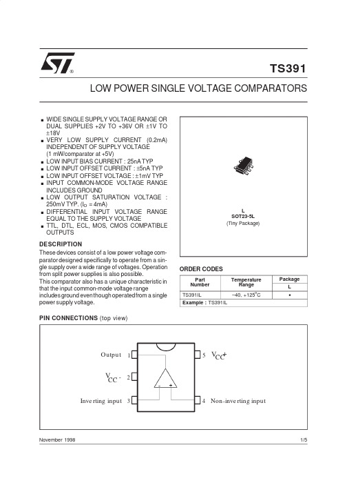
LOW POWER SINGLE VOLTAGE COMPARATORS®.WIDE SINGLE SUPPLY VOLTAGE RANGE OR DUAL SUPPLIES +2V TO +36V OR ±1V TO ±18V.VERY LOW SUPPLY CURRENT (0.2mA)INDEPENDENT OF SUPPLY VOLTAGE (1mW/comparator at +5V).LOW INPUT BIAS CURRENT :25nA TYP .LOW INPUT OFFSET CURRENT :±5nA TYP .LOW INPUT OFFSET VOLTAGE :±1mV TYP .INPUT COMMON-MODE VOLTAGE RANGE INCLUDES GROUND.LOW OUTPUT SATURATION VOLTAGE :250mV TYP.(I O =4mA).DIFFERENTIAL INPUT VOLTAGE RANGE EQUAL TO THE SUPPLY VOLTAGE.TTL,DTL,ECL,MOS,CMOS COMPATIBLE OUTPUTSDESCRIPTIONThese devices consist of a low power voltage com-parator designed specifically to operate from a sin-gle supply over a wide range of voltages.Operation from split power supplies is also possible.This comparator also has a unique characteristic in that the input common-mode voltage rangeincludesground eventhough operatedfrom a single power supply voltage.ORDER CODESPart Number TemperatureRange PackageL TS391IL–40,+125oC•Example :TS391IL12345Inve rting input Non-inve rting inputOutputVCC-V CC+PIN CONNECTIONS (top view)TS391November 1998LSOT23-5L (Tiny Package)1/5ABSOLUTE MAXIMUM RATINGSSymbol ParameterTS391I Unit V CC Supply Voltage±18or 36V V id Differential Input Voltage ±36V V i Input Voltage–0.3to +36VOutput Short-circuit to Ground -note 1Infinite P tot Power Dissipation -note 2500mWT oper Operating Free-air TemperatureRange –40to +125o C T stgStorage Temperature Range–65to +150oCNotes : 1.Short-circuit from the output to V CC +can cause excessive heating and eventual destruction.The maximum outputcurrent is approximately 20mA,independent of the magnitude of V CC +.2.T j =150o C,T a mb =25o C with R t hja =250oC/W for SOT23-5package.Non-invertingInputInverting Input3.5µA 100µA 3.5µA 100µACCV CCV CCV CCV OV SCHEMATIC DIAGRAMTS3912/5ELECTRICAL CHARACTERISTICSV CC+=+5V,V CC–=0V,T amb=25o C(unless otherwise specified)Symbol Parameter Min.Typ.Max.UnitV io Input Offset Voltage–(note2)T amb=+25o CT min.≤T amb≤T max.159mVI ib Input Bias Current–(note3)T amb=+25o CT min.≤T amb≤T max.25250400nAI io Input Offset CurrentT amb=+25o CT min.≤T amb≤T max.550150nAA vd Large Signal Voltage GainV CC=15V,R L=15kΩ,V o=1to11V50200V/mVI CC Supply CurrentV CC=5V,no loadV CC=30V,no load 0.20.50.51.25mAV icm Input Common Mode Voltage Range-(note4) T amb=+25o CT min.≤T amb≤T max.0V CC+-1.5V CC+-2VV id Differential Input Voltage-(note6)V CC+V I sink Output Sink Current(V id=-1V,V O=1.5V)616mA V OL Low Level Output Voltage(V id=-1V,I sink=4mA) T amb=25o CT min.≤T amb≤T max 250400700mVI OH High Level Output Current(V id=1V,V CC=V O=30V) T amb=25o CT min.≤T amb≤T max 0.11nAµAt re Response Time(R L=5.1kΩto V CC+)–(note5) 1.3µst rel Large Signal Response Time(V i=TTL,V ref=+1.4V,R L=5.1kΩto V CC+)300nsNotes: 2.At output swit ch point,V O≈1.4V,R S=0Ωwith V CC+from5V to30V and over the full input common-mode range (0V to V C C+1.5V).3.The direction of the input current is out of the IC due to the PNP input stage.This current is essentially constant,independent of the state of the output,so no loading charge exists on the reference or input lines.4.The input common-mode voltage of either input signal voltage should not be allowed to go negative by more than0.3V.The upper end of the common-mode voltage range is V C C+–1.5V,but either or both inputs can go to+30V without damage.5.The response time specified is for a100mV input step with5mV overdrive.For larger overdrive signals300ns canbe obtained.6.Positive excursions of input voltage may exceed the power supply level.As long as the other voltage remains withinthe common-mode range the comparator will provide a proper output state.The low input voltage state must not be less than–0.3V(or0.3V below the negative power supply,if used).TS3913/5S U P P L Y C U R R E N T (m A )0.50.40.30.20.110203040S UP P LY VOLTAGE (V)T a m b =+70CT amb =+125CT=+25CT a mb =0CT a mb =-55CR =SUPPLY CURRENT versusSUPPLY VOLTAGEI N P U T C U R R E N T (n A )2010203040SUPPLY VOLTAGE (V)T amb =+70°CT amb =+125°CT amb =-55°C4060800T amb =0°CT amb =+25°CV =0Vi R =10Ωi 9INPUT CURRENT versus SUPPLY VOLTAGET amb =-55°CT amb =+125°CT amb =+25°COut of saturation10110-310-210-1100S A T U R A T I O N V O L T A G E (V )10-210-1100101102OUTPUT SINK CURRENT (mA)OUTPUT SATURATION VOLTAGEversus OUTPUT CURRENT5V5.1k Ωe oe I65432100-50-100I N P U T V O L T A G E (m V )O U T P U T V O L T A G E (V )0.51 1.52TIME (µs)Input overdrive :5mV 20mV 100mVT amb =+25°CRESPONSE TIME FOR VARIOUS INPUT OVERDRIVES -NEGATIVE TRANSITION5V5.1k Ωe oe654321010050I N P U T V O L T A G E (m V )O U T P U T V O L T A G E (V )0.51 1.52TIME (µs)Input overdrive :100mV 20mV 5mV T amb =+25°C 0RESPONSE TIME FOR VARIOUS INPUT OVERDRIVES -POSITIVE TRANSITIONTS3914/5LCE1A2AA1bEDPACKAGE MECHANICAL DATA 5PINS -TINY PACKAGE (SOT23)limetersInchesMin.Max.Min.Max.A 0.90 1.450.0340.057A100.150.006A20.90 1.300.0340.051b 0.350.500.0130.020C 0.090.200.0030.008D 2.80 3.000.1100.118E 2.60 3.000.1020.118E1 1.50 1.750.0590.069L0.100.600.0030.024Information furnished is believed to be accurate and reliable.However,STMicroelectronics assumes no responsibility for the consequences of use of such information nor for any infringement of patents or other rights of third parties which may result from its use.No license is granted by implication or otherwise under any patent or patent rights of STMicroelectronics.Specifications mentioned in this publication are subject to change without notice.This publ ication supersedes and replaces all information previously supplied.STMicroelectronics products are not authorized for use as critical components in life support devices or systems without express written approval of STMicroelectronics.©The ST logo is a trademark of STMicroelectronics©1998STMicroelectronics –Printed in Italy –All Rights ReservedSTMicroelectronics GROUP OF COMPANIESAustralia -Brazil -Canada -China -France -Germany -Italy -Japan -Korea -Malaysia -Malta -Mexico -MoroccoThe Netherlands -Singapore -Spain -Sweden -Switzerland -Taiwan -Thailand -United Kingdom -U.S.A.©O R D E R C O D ETS3915/5。


IR Receiver Modules for Remote Control SystemsTSOP392.., TSOP394.. Vishay SemiconductorsMECHANICAL DATA Pinning:1 = OUT,2 = V S,3 = GND FEATURES•Very low supply current•Photo detector and preamplifier in one package •Internal filter for PCM frequency•Improved shielding against EMI•Supply voltage: 2.5 V to 5.5 V•Improved immunity against ambient light•Insensitive to supply voltage ripple and noise •Component in accordance to RoH S 2002/95/EC and WEEE 2002/96/ECDESCRIPTIONThe TSOP392.., TSOP394.. series are miniaturized receivers for infrared remote control systems. A PIN diode and a preamplifier are assembled on a lead frame, the epoxy package acts as an IR filter.The demodulated output signal can be directly decoded by a microprocessor. The TSOP392.. is compatible with all common IR remote control data formats. The TSOP394.. is optimized to suppress almost all spurious pulses from energy saving fluorescent lamps but will also suppress some data signals.This component has not been qualified according to automotive specifications.BLOCK DIAGRAM APPLICATION CIRCUIT19026PARTS TABLECARRIER FREQUENCY STANDARD APPLICATIONS (AGC2/AGC8)VERY NOISY ENVIRONMENTS (AGC4) 30 kHz TSOP39230TSOP3943033 kHz TSOP39233TSOP3943336 kHz TSOP39236TSOP3943638 kHz TSOP39238TSOP3943840 kHz TSOP39240TSOP3944056 kHz TSOP39256TSOP39456TSOP392.., TSOP394..IR Receiver Modules for Remote Control SystemsVishay SemiconductorsNote(1)Stresses beyond those listed under “Absolute Maximum Ratings” may cause permanent damage to the device. This is a stress rating only and functional operation of the device at these or any other conditions beyond those indicated in the operational sections of this specification is not implied. Exposure to absolute maximum rating condtions for extended periods may affect the device reliability.Note (1)T amb = 25°C, unless otherwise specifiedTYPICAL CHARACTERISTICST amb = 25°C, unless otherwise specifiedFig. 1 - Output Active LowFig. 2 - Pulse Length and Sensitivity in Dark AmbientABSOLUTE MAXIMUM RATINGS (1)PARAMETER TEST CONDITIONSYMBOLVALUE UNIT Supply voltage (pin 2)V S - 0.3 to + 6.0V Supply current (pin 2)I S 3mA Output voltage (pin 1)V O - 0.3 to (V S + 0.3)V Output current (pin 1)I O 5mA Junction temperatureT j 100°C Storage temperature range T stg - 25 to + 85°C Operating temperature range T amb - 25 to + 85°C Power consumption T amb ≤ 85°C P tot 10mW Soldering temperaturet ≤ 10 s, 1 mm from case T sd260°CELECTRICAL AND OPTICAL CHARACTERISTICS (1)PARAMETER TEST CONDITION SYMBOL MIN.TYP.MAX.UNIT Supply current (pin 2)E v = 0, V S = 3.3 V I SD 0.270.350.45mA E v = 40 klx, sunlightI SH 0.45mA Supply voltage V S 2.55.5V Transmission distance E v = 0, test signal see fig. 1,IR diode TSAL6200,I F = 250 mA d 45m Output voltage low (pin 1)I OSL = 0.5 mA, E e = 0.7 mW/m 2,test signal see fig. 1V OSL 100mV Minimum irradiance Pulse width tolerance:t pi - 5/f o < t po < t pi + 6/f o ,test signal see fig. 1E e min.0.150.35mW/m 2Maximum irradiance t pi - 5/f o < t po < t pi + 6/f o ,test signal see fig. 1E e max.30W/m 2DirectivityAngle of half transmission distanceϕ1/2± 45degE eV O V VTSOP392.., TSOP394..Vishay SemiconductorsIR Receiver Modules for Remote Control SystemsFig. 3 - Output FunctionFig. 4 - Output Pulse DiagramFig. 5 - Frequency Dependence of ResponsivityFig. 6 - Sensitivity in Bright AmbientFig. 7 - Sensitivity vs. Supply Voltage DisturbancesFig. 8 - Sensitivity vs. Electric Field DisturbancesE eV O V V OL0.00.20.40.60.81.01.20.70.9 1.1 1.3f/f 0 - Relati v e Fre qu ency16925E /E - R e l. R e s p o n s i v i t y e m i n.eTSOP392.., TSOP394.. IR Receiver Modules forRemote Control SystemsVishay SemiconductorsFig. 9 - Maximum Envelope Duty Cycle vs. Burst Length Fig. 10 - Sensitivity vs. Ambient Temperature Fig. 11 - Relative Spectral Sensitivity vs. WavelengthFig. 12 - Horizontal DirectivityFig. 13 - Vertical Directivity Fig. 14 - Sensitivity vs. Supply VoltageTSOP392.., TSOP394..Vishay SemiconductorsIR Receiver Modules for Remote Control SystemsSUITABLE DATA FORMATThe TSOP392.., TSOP394.. series are designed to suppress spurious output pulses due to noise or disturbance signals.Data and disturbance signals can be distinguished by the devices according to carrier frequency, burst length and envelope duty cycle. The data signal should be close to the band-pass center frequency (e.g. 38 kH z) and fulfill the conditions in the table below.When a data signal is applied to the TSOP392.., TSOP394..in the presence of a disturbance signal, the sensitivity of the receiver is reduced to insure that no spurious pulses are present at the output. Some examples of disturbance signals which are suppressed are:•DC light (e.g. from tungsten bulb or sunlight)•Continuous signals at any frequency•Strongly or weakly modulated noise from fluorescent lamps with electronic ballasts (see figure 15 or figure 16)Fig. 15 - IR Signal from Fluorescent Lampwith Low ModulationFig. 16 - IR Signal from Fluorescent Lampwith High ModulationNoteFor data formats with short bursts please see the datasheet for TSOP391.., TSOP393..0101520Time (ms)16920I R S i g n a l50101520Time (ms)16921I R S i g n a l10TSOP392..TSOP394..Minimum burst length10 cycles/burst 10 cycles/burst After each burst of lengtha minimum gap time is required of10 to 70 cycles ≥ 10 cycles 10 to 35 cycles ≥ 10 cycles For bursts greater thana minimum gap time in the data stream is needed of 70 cycles > 4 x burst length35 cycles> 10 x burst lengthMaximum number of continuous short bursts/second 18001500Compatible to NEC code yes yes Compatible to RC5/RC6 code yes yes Compatible to Sony codeyes no Compatible to Thomson 56 kHz codeyes yes Compatible to Mitsubishi code (38 kHz, preburst 8 ms, 16 bit)yes no Compatible to Sharp codeyesyesSuppression of interference from fluorescent lampsMost common disturbance signals are suppressedEven extreme disturbance signals are suppressedTSOP392.., TSOP394..IR Receiver Modules forVishay SemiconductorsRemote Control SystemsPACKAGE DIMENSIONS in millimetersTSOP392.., TSOP394..Vishay Semiconductors IR Receiver Modules forRemote Control SystemsOZONE DEPLETING SUBSTANCES POLICY STATEMENTIt is the policy of Vishay Semiconductor GmbH to1.Meet all present and future national and international statutory requirements.2.Regularly and continuously improve the performance of our products, processes, distribution and operating systems withrespect to their impact on the health and safety of our employees and the public, as well as their impact on the environment. It is particular concern to control or eliminate releases of those substances into the atmosphere which are known as ozone depleting substances (ODSs).The Montreal Protocol (1987) and its London Amendments (1990) intend to severely restrict the use of ODSs and forbid their use within the next ten years. Various national and international initiatives are pressing for an earlier ban on these substances. Vishay Semiconductor GmbH has been able to use its policy of continuous improvements to eliminate the use of ODSs listed in the following documents.1.Annex A, B and list of transitional substances of the Montreal Protocol and the London Amendments respectively.2.Class I and II ozone depleting substances in the Clean Air Act Amendments of 1990 by the Environmental Protection Agency(EPA) in the USA.3.Council Decision 88/540/EEC and 91/690/EEC Annex A, B and C (transitional substances) respectively.Vishay Semiconductor GmbH can certify that our semiconductors are not manufactured with ozone depleting substances and do not contain such substances.We reserve the right to make changes to improve technical designand may do so without further notice.Parameters can vary in different applications. All operating parameters must be validated for each customer application by the customer. Should the buyer use Vishay Semiconductors products for any unintended or unauthorized application, the buyer shall indemnify Vishay Semiconductors against all claims, costs, damages, and expenses, arising out of, directly or indirectly, any claim of personal damage, injury or death associated with such unintended or unauthorized use.Vishay Semiconductor GmbH, P.O.B. 3535, D-74025 Heilbronn, GermanyDisclaimer Legal Disclaimer NoticeVishayAll product specifications and data are subject to change without notice.Vishay Intertechnology, Inc., its affiliates, agents, and employees, and all persons acting on its or their behalf (collectively, “Vishay”), disclaim any and all liability for any errors, inaccuracies or incompleteness contained herein or in any other disclosure relating to any product.Vishay disclaims any and all liability arising out of the use or application of any product described herein or of any information provided herein to the maximum extent permitted by law. The product specifications do not expand or otherwise modify Vishay’s terms and conditions of purchase, including but not limited to the warranty expressed therein, which apply to these products.No license, express or implied, by estoppel or otherwise, to any intellectual property rights is granted by this document or by any conduct of Vishay.The products shown herein are not designed for use in medical, life-saving, or life-sustaining applications unless otherwise expressly indicated. Customers using or selling Vishay products not expressly indicated for use in such applications do so entirely at their own risk and agree to fully indemnify Vishay for any damages arising or resulting from such use or sale. Please contact authorized Vishay personnel to obtain written terms and conditions regarding products designed for such applications.Product names and markings noted herein may be trademarks of their respective owners.元器件交易网。