Excitonic Effects and Optical Spectra of Single-Walled Carbon Nanotubes
- 格式:pdf
- 大小:232.82 KB
- 文档页数:6
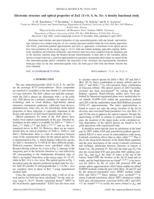
Electronic structure and optical properties of Zn X(X=O,S,Se,Te):A density functional study S.Zh.Karazhanov,1,2P.Ravindran,1A.Kjekshus,1H.Fjellvåg,1and B.G.Svensson3 1Centre for Material Science and Nanotechnology,Department of Chemistry,University of Oslo,P.O.Box1033Blindern,N-0315Oslo,Norway2Physical-Technical Institute,2B Mavlyanov Street,Tashkent700084,Uzbekistan3Department of Physics,University of Oslo,P.O.Box1048Blindern,N-0316Oslo,Norway͑Received5July2006;revised manuscript received15November2006;published6April2007͒Electronic band structure and optical properties of zinc monochalcogenides with zinc-blende-and wurtzite-type structures were studied using the ab initio density functional method within the local-density approxima-tion͑LDA͒,generalized-gradient approximation,and LDA+U approaches.Calculations of the optical spectrahave been performed for the energy range0–20eV,with and without including spin-orbit coupling.Reflec-tivity,absorption and extinction coefficients,and refractive index have been computed from the imaginary partof the dielectric function using the Kramers-Kronig transformations.A rigid shift of the calculated opticalspectra is found to provide a goodfirst approximation to reproduce experimental observations for almost all thezinc monochalcogenide phases considered.By inspection of the calculated and experimentally determinedband-gap values for the zinc monochalcogenide series,the band gap of ZnO with zinc-blende structure hasbeen estimated.DOI:10.1103/PhysRevB.75.155104PACS number͑s͒:71.15.Ϫm,71.22.ϩiI.INTRODUCTIONThe zinc monochalcogenides͑Zn X;X=O,S,Se,and Te͒are the prototype II-VI semiconductors.These compoundsare reported to crystallize in the zinc-blende-͑z͒and wurtzite ͑w͒-type structures.The Zn X-z phases are optically isotropic, while the Zn X-w phases are anisotropic with c as the polaraxis.Zn X phases are a primary candidate for optical devicetechnology such as visual displays,high-density opticalmemories,transparent conductors,solid-state laser devices,photodetectors,solar cells,etc.So,knowledge about opticalproperties of these materials is especially important in thedesign and analysis of Zn X-based optoelectronic devices.Optical parameters for some of the Zn X phases havewidely been studied experimentally in the past.Detailed in-formation on this subject is available for ZnO-w,1–9ZnS-w,9ZnS-z,9–11ZnSe-z,9,10and ZnTe-z,9,10,12,13and see the sys-tematized survey in Ref.14.However,there are no experi-mental data on optical properties of ZnSe-w,ZnTe-w,andZnO-z.Furthermore,there is a lack of consistency betweensome of the experimental values for the optical spectra.Thisis demonstrated in Fig.1,which displays reflectivity spectrafor ZnO-w measured at T=300K by three different groups.Dielectric-response functions were calculated using theKramers-Kronig relation.As is seen in Fig.1,intensity of theimaginary part of the dielectric function͑⑀2͒and reflectivity ͑R͒corresponding to the fundamental absorption edge of ZnO-w are higher8than those at the energy range10–15eV, while in Ref.14it is vice versa.The optical spectra in Fig.1 measured using the linearly polarized incident light for elec-tricfield͑E͒parallel͑ʈ͒and perpendicular͑Ќ͒to the c axes are somehow close to those of Ref.7using nonpolarized incident light.Using the experimental reflectivity data,a full set of op-tical spectra for ZnO has been calculated15for the wide en-ergy range0–26eV.Density functional theory16͑DFT͒in the local-density approximation17͑LDA͒has also been used to calculate optical spectra for ZnO-w͑Ref.18͒and ZnS-w ͑Ref.18͒by linear combination of atomic orbitals and for ZnS-z19and ZnSe-z19by self-consistent linear combination of Gaussian orbitals.The optical spectra of ZnO͑including excitons͒has been investigated20by solving the Bethe-Salpeter equation.Band-structure studies have been per-formed by linearized-augmented plane-wave method plus lo-cal orbitals͑LAPW+LO͒within the generalized gradient and LDA with the multiorbital mean-field Hubbard potential ͑LDA+U͒approximations.The latter approximation is found to correct not only the energy location of the Zn3d electrons and associated band parameters͑see also Refs.21 and22͒but also to improve the optical response.Despite the shortcoming of DFT in relation to underestimation of band gaps,the locations of the major peaks in the calculated en-ergy dependence of the optical spectra are found to be in good agreement with experimental data.It should be noted that the error in calculation of the band gap by DFT within LDA and generalized-gradient approxi-mation͑GGA͒is more severe in semiconductors with strong Coulomb correlation effects than in other solids.21–25This is due to the mean-field character of the Kohn-Sham equations and the poor description of the strong Coulomb correlation and exchange interaction between electrons in narrow d bands͑viz.,the potential U͒.Not only the band gap͑E g͒but also the crystal-field͑CF͒and spin-orbit͑SO͒splitting ener-gies͑⌬CF and⌬SO͒,the order of states at the top of the valence band͑VB͒,the location of the Zn3d band and its width,and the band dispersion are found21,22,26,27to be incor-rect for ZnO-w by the ab initio full potential͑FP͒and atomic-sphere-approximation͑ASA͒linear muffin-tin orbital ͑LMTO͒methods within the pure LDA͑Refs.26and27͒and by the projector-augmented wave͑PAW͒method within LDA and GGA.21,22Thesefindings were ascribed21,22to strong Coulomb correlation effects.DFT calculations within LDA plus self-interaction correction͑LDA+SIC͒and LDA +U are found21,22,26to rectify the errors related to⌬CF andPHYSICAL REVIEW B75,155104͑2007͒⌬SO ,order of states at the top VB,and width and location of the Zn 3d band,as well as effective masses.In other semi-conductors,in which the Coulomb correlation is not suffi-ciently strong,the ⌬CF and ⌬SO values derived from DFT calculations within LDA are found to be quite accurate.This was demonstrated for diamondlike group IV ,z -type group III-V ,II-VI,and I-VII semiconductors,28w -type AlN,GaN,and InN,29using the LAPW and V ASP -PAW,the w -type CdS and CdSe,27z -type ZnSe,CdTe,and HgTe,30using the ab initio LMTO-ASA,and z -and w -type ZnSe and ZnTe ͑Refs.21and 22͒as well as z -type CdTe,31using the V ASP -PAW and FP LMTO methods.Although the SO splitting at the top of VB is known to play an important role in electronic structure and chemical bonding ofsemiconductors,21,22,26,28–30,32,33there is no systematic study of the role of the SO coupling in optical properties of these materials.Several attempts have been undertaken to resolve the DFT eigenvalue problem.One such approach is the utilization of the GW approximation ͑“G”stands for one-particle Green’s function as derived from many-body perturbation theory and “W”for Coulomb screened interactions ͒.Although GW re-moves most of the problems of LDA with regard to excited-state properties,it fails to describe the semiconductors with strong Coulomb correlation effects.For example,two studies of the band gap of ZnO calculated using the GW correction underestimated E g by 1.2eV ͑Ref.34͒and overestimated it by 0.84eV.35Calculations for Zn,Cd,and Hg monochalco-genides by the GW approach showed 36that the band-gap underestimation is in the range 0.3–bination of exact-exchange ͑EXX ͒DFT calculations and the optimized-effective GW potential approach is found 37to improve the agreement with the experimental band gaps and Zn 3d en-ergy levels.Band gaps calculated within the EXX treatment are found to be in good agreement with experiment for thes -p semiconductors.38,39Excellent agreement with experi-mental data was obtained 39also for locations of energy levels of the d bands of a number of semiconductors and insulators such as Ge,GaAs,CdS,Si,ZnS,C,BN,Ne,Ar,Kr,and Xe.Another means to correct the DFT eigenvalue error is to use the screened-exchange LDA.40Compared to LDA and GW,this approximation is found to be computationally much less demanding,permitting self-consistent determination of the ground-state properties and giving more correct band gaps and optical properties.Other considered approaches for ab initio computations of optical properties involve electron-hole interaction,41partial inclusion of dynamical vertex cor-rections that neglect excitons,42and empirical energy-dependent self-energy correction according to the Kohn-Sham local-density theory of excitation.19However,the simplest method is to apply the scissor operator,43which displaces the LDA eigenvalues for the unoccupied states by a rigid energy ing the latter method,excellent agree-ment with experiments has been demonstrated for lead monochalcogenides 44and ferroelectric NaNO 2.45However,the question as to whether the rigid energy shift is generally applicable to semiconductors with strong Coulomb correla-tion effects is open.In this work,electronic structure and optical properties of the Zn X -w and -z phases have been studied in the energy range from 0to 20eV based on first-principles band-structure calculations derived from DFT within the LDA,GGA,and LDA+U .PUTATIONAL DETAILSExperimentally determined lattice parameters have been used in the present ab initio calculations ͑Table I ͒.The ideal positional parameter u for Zn X -w is calculated on the as-sumption of equal nearest-neighbor bond lengths:27u =13ͩa cͪ2+14.͑1͒The values of u for the ideal case agree well with the experi-mental values u *͑see Table I ͒.Self-consistent calculations were performed using a 10ϫ10ϫ10mesh according to the Monkhorst-Pack scheme for the Zn X -z phases and the ⌫-centered grid for the Zn X -w phases.A.Calculations byV ASPpackageOptical spectra have been studied based on the band-structure data obtained from the V ASP -PAW package,55which solves the Kohn-Sham eigenvalues in the framework of the DFT ͑Ref.16͒within LDA,17GGA,56and the simplified ro-tationally invariant LDA+U .23,24The exchange and correla-tion energies per electron have been described by the Perdew-Zunger parametrization 57of the quantum Monte Carlo results of Ceperley and Alder.58The interaction be-tween electrons and atomic cores is described by means of non-norm-conserving pseudopotentials implemented in the V ASP package.55The pseudopotentials are generated in accor-dance with the PAW ͑Refs.59and 60͒method.The use of the PAW pseudopotentials addresses the problem ofinad-FIG.1.Reflectivity spectra R ͑͒for ZnO-w determined experi-mentally at 300K in Refs.9and 14͑solid circles ͒,Ref.8͑open circles ͒,and Ref.7͑solid lines ͒,along with the imaginary part of the dielectric-response function ͓⑀2͔͑͒calculated using the Kramers-Kronig relation.The results of Ref.7͑open circles ͒are used for both E ʈc and E Ќc ,because no polarized incident light was used in the experiments.KARAZHANOV et al.PHYSICAL REVIEW B 75,155104͑2007͒equate description of the wave functions in the core region ͑common to other pseudopotential approaches61͒,and its ap-plication allows us to construct orthonormalized all-electron-like wave functions for Zn3d and4s and s and p valence electrons of the X atoms under consideration.LDA and GGA pseudopotentials have been used,and the completelyfilled semicore Zn3d shell has been considered as valence states.It is well known that DFT calculations within LDA and GGA locate the Zn3d band inappropriately close to the top-most VB,hybridizing the O p band,falsifying the band dis-persion,and reducing the band gap.Nowadays,the problem is known to be solved by using the LDA+SIC and LDA +U.21,22,26,62–64For the DFT calculations within LDA+U, explicit values of the parameters U and J are required as input.In previous papers,21,22we have estimated the values of the U and J parameters within the constrained DFT theory65and in a semiempirical way by performing the cal-culations for different values of U and forcing it to match the experimentally established66location of the Zn3d bands. Based on the results,21,22the values of the parameters U and J listed in Table I are chosen to study the optical spectra.B.Calculations by MINDLAB packageFor investigation of the role of the SO coupling in elec-tronic structure and optical properties of Zn X,DFT calcula-tions have been performed using the MINDLAB package,67 which uses the full potential linear muffin-tin orbital͑FP LMTO͒method.For the core charge density,the frozen-core approximation is used.The calculations are based on LDA with the exchange-correlation potential parametrized accord-ing to Gunnarsson-Lundquist68and V osko-Wilk-Nussair.69The base geometry in this computational method consists of a muffin-tin part and an interstitial part.The basis set is comprised of linear muffin-tin orbitals.Inside the muffin-tin spheres,the basis functions,charge density,and potential are expanded in symmetry-adapted spherical harmonic functions together with a radial function and a Fourier series in the interstitial.C.Calculation of optical propertiesFrom the DFT calculations,the imaginary part of the di-electric function⑀2͑͒has been derived by summing transi-tions from occupied to unoccupied states for energies much larger than those of the phonons:⑀2ij͑͒=Ve22បm22͵d3k͚nnЈ͗kn͉p i͉knЈ͘ϫ͗knЈ͉p j͉kn͘f kn͑1−f knЈ͒␦͑⑀knЈ−⑀kn−ប͒.͑2͒Here,͑p x,p y,p z͒=p is the momentum operator,f kn the Fermi distribution,and͉kn͘the crystal wave function correspond-ing to the energy⑀kn with momentum k.Since the Zn X-w phases are optically anisotropic,components of the dielectric function corresponding to the electricfield parallel͑Eʈc͒and perpendicular͑EЌc͒to the crystallographic c axis have been considered.The Zn X-z phases are isotropic;conse-quently,only one component of the dielectric function has to be analyzed.The real part of the dielectric function⑀1͑͒is calculated using the Kramer-Kronig transformation.The knowledge ofTABLE I.Theoretically and experimentally͑in brackets͒determined unit-cell dimensions a and c,vol-umes V,ideal u͓calculated by Eq.͑1͔͒,and experimental u*,as well as values of the parameters U and J from Refs.21and22,were used in the present calculations.For w-type structure,a=b.For the z-type structure, a=b=c and all atoms are infixed positions.Phasea͑Å͒c͑Å͒V͑Å3͒u*uU͑eV͒J͑eV͒ZnO-w a 3.244͑3.250͒ 5.027͑5.207͒45.82͑47.62͒0.3830.38091ZnS-w b,c 3.854͑3.811͒ 6.305͑6.234͒81.11͑78.41͒0.3750.37561ZnSe-w a,d 4.043͑3.996͒ 6.703͑6.626͒94.88͑91.63͒0.3750.37181ZnTe-w e,f 4.366͑4.320͒7.176͑7.100͒118.47͑114.75͒0.3750.37371ZnO-z g 4.633͑4.620͒99.45͑98.61͒81ZnS-z h,i 5.451͑5.409͒161.99͑158.25͒91ZnSe-z a 5.743͑5.662͒189.45͑181.51͒81ZnTe-z i,j 6.187͑6.101͒236.79͑227.09͒81Reference46.b Reference18.c Reference47.d Reference48.e Reference49.f Reference50.g Reference51.h Reference52.i Reference53.j Reference54.ELECTRONIC STRUCTURE AND OPTICAL PROPERTIES…PHYSICAL REVIEW B75,155104͑2007͒both the real and imaginary parts of the dielectric tensor allows one to calculate other important optical spectra.In this paper,we present and analyze the reflectivity R ͑͒,the absorption coefficient ␣͑͒,the refractive index n ͑͒,and the extinction coefficient k ͑͒:R ͑͒=ͯͱ⑀͑͒−1ͱ⑀͑͒+1ͯ2,͑3͒␣͑͒=ͱ2ͱ⑀12͑͒+⑀22͑͒−2⑀1͑͒,͑4͒n ͑͒=ͱͱ⑀12͑͒+⑀22͑͒+⑀1͑͒2,͑5͒k ͑͒=ͱͱ⑀12͑͒+⑀22͑͒−⑀1͑͒2.͑6͒Here,⑀͑͒=⑀1͑͒+i ⑀2͑͒is the complex dielectric function.The calculated optical spectra yield unbroadened functions and,consequently,have more structure than the experimental ones.44,45,70,71To facilitate a comparison with the experimen-tal findings,the calculated imaginary part of the dielectric function has been broadened.The exact form of the broad-ening function is unknown.However,analysis of the avail-able experimentally measured optical spectra of Zn X shows that the broadening usually increases with increasing excita-tion energy.Also,the instrumental resolution smears out many fine features.These features have been modeled using the lifetime broadening technique by convoluting the imagi-nary part of the dielectric function with a Lorentzian with a full width at half maximum of 0.002͑ប͒2eV,increasing quadratically with the photon energy.The experimental reso-lution was simulated by broadening the final spectra with a Gaussian,where the full width at half maximum is equal to 0.08eV.III.RESULTS AND DISCUSSIONA.Band structureThe optical spectra are related to band dispersion and probabilities of interband optical transitions.So,it is of in-terest to analyze the electronic structure in detail.Band dis-persions for Zn X -w and Zn X -z calculated by DFT within LDA and LDA+U are presented in Fig.2.The general fea-tures of the band dispersions are in agreement with previous studies ͑see,e.g.,Refs.26,62,and 72͒.It is seen from Fig.2that the conduction-band ͑CB ͒minima for Zn X -w and Zn X -z are much more dispersive than the VB maximum,which shows that the holes are much heavier than the CB electrons in agreement with experimental data 73,74for the effective masses and calculated with FP LMTO and ͑Ref.26͒linear combination of atomic orbitals,18as well as with our findings.21,21Consequently,mobility of electrons is higher than that of holes.Furthermore,these features indicate that p electrons of X ͑that form the topmost VB states ͒are tightly bound to their atoms and make the VB holes less mobile.Hence,the contribution of the holes to the conductivity is expected to be smaller than that of CB electrons even though the concentration of the latter is smaller than that of the former.These features emphasize the predominant ionic na-ture of the chemical bonding.Another interesting feature of the band structures is that the VB maximum becomes more dispersive with increasing atomic number of X from O to Te.As noted in our previous contributions,21,22the band gaps of Zn X calculated by DFT within LDA,GGA,and LDA +U are underestimated and the question as to whether it is possible to shift the CB states rigidly was kept open.As found from the optical spectra discussed on the following sections,rigid shifts of the CB states up to the experimen-tally determined locations can provide a good first approxi-mation for the stipulation of the band gap.So,for the band dispersions in Fig.2,we have made use of this simple way for correcting the band gaps calculated by DFT.The only problem in this respect was the lack of an experimental band-gap value for ZnO-z .To solve this problem,the experi-mental and calculated ͑by DFT within LDA ͒band gaps ͑E g ͒of the Zn X series were plotted as a function of the atomic number of X .As seen from Fig.3,E g for the Zn X -w phases are very close to the corresponding values for the Zn X -z phases and the shape of the experimentaland calculated functional dependencies is in conformity.On this basis,theFIG.2.Band dispersion for ZnO-w ,ZnS-w ,ZnSe-w ,ZnTe-w ,ZnO-z ,ZnS-z ,ZnSe-z ,and ZnTe-z calculated according to LDA ͑solid lines ͒and LDA+U ͑dotted lines ͒.The Fermi level is set to zero energy.KARAZHANOV et al.PHYSICAL REVIEW B 75,155104͑2007͒band gap of ZnO-z is estimated by extrapolating the findings for Zn X -z from ZnS-z to ZnO-z .This procedure gave E g Ϸ3.3eV for ZnO-z .It is well known that not only band gaps are underesti-mated within LDA and GGA,but also band dispersions come out incorrectly,whereas location of energy levels of the Zn 3d electrons are overestimated ͑see,e.g.,Refs.20–22and 63͒.As also seen from Fig.2,calculations within the LDA+U approach somewhat correct the location of the en-ergy levels of the Zn 3d electrons.The elucidation of the eigenvalue problem and the order of states at the topmost VB from LDA,GGA,and LDA+U calculations are discussed in Refs.20–22and 26and will not be repeated here.Examination of Fig.2shows that the VB comprises three regions of bands:first a lower region consists of s bands of Zn and X ,a higher-lying region of well localized Zn 3d bands,and on top of this a broader band dispersion originat-ing from X -p states hybridized with Zn 3d states.The latter subband is more pronounced in ZnO than in the other Zn X phases considered.The hybridization is most severe accord-ing to the LDA and GGA calculations,whereas the LDA +U calculations somehow suppress this and improve the band-gap underestimation.A more detailed discussion of these aspects is found in Refs.21and 22.The SO splitting at the topmost VB is known to play an important role for the electronic structure and chemical bonding of solids.28,29,32In semiconductors with z -type struc-ture,the SO splitting energy is determined as the difference between energies of the topmost VB states with symmetry ⌫8v and ⌫7v .28,29,32In the w -type compounds,the topmost VB is split not only by SO interaction but also by CF,giving rise to three states at the Brillouin-zone center.To calculate theSO splitting energy for w -type phases,the quasicubic model of Hopfield 75is commonly used.It is well known that the SO splitting energy derived from ab initio calculations agrees well with experimental data only for some of the semiconductors.This is demonstrated,for example,for all diamondlike group IV and z -type group III-V ,II-VI,and I-VII semiconductors,28w -type AlN,GaN,and InN,29Zn X -w and -z ͑X =S,Se,and Te ͒,21,22and CdTe.31However,the errors in estimated SO and CF splitting ener-gies by LDA calculations are significant for semiconductors with strong Coulomb correlation effects,as demonstrated,e.g.,for ZnO.21,22,26For such systems,DFT calculations within LDA+U ͑Refs.21,22,and 26͒are shown to provide quite accurate values for ⌬CF and ⌬SO .Overestimation of the p -d hybridization in various variants of the DFT can also lead to the wrong spin-orbit coupling of the valence bands.76,77Systematic study of the SO coupling parameters was per-formed for zinc-blende II-VI semiconductors ͑Ref.30͒using the TB and LMTO methods,as well as for all diamondlike and zinc-blende semiconductors ͑Ref.28͒using the FLAPW method with and without the p 1/2local orbitals and the frozen-core PAW method implemented into V ASP .The cor-rections coming from the inclusion of the local p 1/2orbitals are found to be negligible for the compounds with light at-oms.Analysis of these results shows that the SO splitting energy coming from calculations using the V ASP -PAW shows good agreement with the experimental data.This result was also obtained 21recently for Zn X of wurtzite and zinc-blende structures.As demonstrated in Refs.21and 22the SO split-ting energy ͑⌬SO ͒increases when one moves from ZnO-z to ZnTe-z ,in agreement with earlier findings of Ref.28.To study the role of the SO coupling in band dispersion,the present ab initio calculations have been performed by V ASP and MINDLAB packages and spin-orbit splitting energy is found.The results are presented in Table II .Analysis of Table II shows that ͑⌬SO ͒calculated by MINDLAB is quite accurate.As expected,band dispersions calculated with and with-out the SO coupling differ little when the SO splittingenergyFIG.3.Band gaps for Zn X -w ͑circles ͒and Zn X -z ͑triangles ͒phases determined experimentally ͑filled symbols,from Refs.21and 22͒and calculated ͑open symbols ͒by DFT within LDA as a function of the atomic number of the X component of Zn X .TABLE II.Calculated SO splitting energy ͑in meV ͒using the MINDLAB package along with the previous theoretical and experi-mental findings.ZnO-z ZnS-z ZnSe-z ZnTe-z –3166432914–3166432914−34a 66a 393a 889a −34b 66b 398b 916b −37c 64c 392c 898c −33d64d 393d 897d 65e420f910fLAPW,Ref.28.b LAPW+p1/2,Ref.28.c V ASP -PAW,Ref.28.dV ASP -PAW,Ref.21.eExperiment,Ref.78.f Experiment,Ref.79.ELECTRONIC STRUCTURE AND OPTICAL PROPERTIES …PHYSICAL REVIEW B 75,155104͑2007͒is small.However,the difference increases when one moves from ZnO to ZnTe.This feature is demonstrated in Table II and Fig.4for band dispersions of ZnO-z ,ZnO-w ,ZnTe-z ,and ZnTe-w calculated by V ASP with and without including the SO coupling.As is well known ͑see,e.g.,Refs.21,26,and 27͒,without the SO coupling,the top of the VB of Zn X -w is split into a doublet and a singlet state.In the band structure,the Fermi level is located at the topmost one ͑Fig.4͒,which is the zero energy.Upon inclusion of the SO cou-pling into calculations,the doublet and singlet states are split into three twofold degenerate states called A ,B ,and C states with energies E g ͑A ͒,E g ͑B ͒,and E g ͑C ͒,respectively,80ar-ranged in order of decreasing energy,i.e.,E g ͑A ͒ϾE g ͑B ͒ϾE g ͑C ͒.The center of gravity of the A ,B ,and C states,located at ͓E g ͑A ͒−E g ͑C ͔͒/3below the topmost A state,re-mains to be nearly the same as the topmost VB,correspond-ing to the case without the SO coupling.26,27Consequently,to compare band structures calculated with and without the SO coupling,one should plot the band structure with the Fermi energy at the center of gravity of the A ,B ,and C states for the former and at the topmost VB for the latter.Hence,when the SO coupling is applied,the A and B states as well as the bottommost CB move upwards to ͓E g ͑A ͒−E g ͑C ͔͒/3in en-ergy,whereas the C state moves downwards to ͓E g ͑A ͒−E g ͑C ͔͒2/3compared to the center of gravity.Then,posi-tions of the lowest VB region calculated with and without the SO coupling remain nearly identical.B.General features of optical spectra of Zn XSince optical properties of solids are based on the band structure,the nature of the basic peaks in the optical spectracan be interpreted in terms of the interband transitions re-sponsible for the peaks.Such an interpretation is available for semiconductors with z -and w -type structures.11,14,81In order to simplify the presentation of the findings of this work,the labels E 0,E 1,and E 2of Ref.11͑from the reflec-tivity spectra ͒were retained in Table III and Fig.4.The subscript 0is ascribed to transitions occurring at ⌫,the sub-script 1to transitions at points in the ͓111͔direction,and the subscript 2to transitions at points in the ͓100͔direction ͑re-ferring to the k space for the z -type structure ͒.Assignment of the E 0,E 1,and E 2peaks to optical transitions at high-symmetry points is presented in Table III and Fig.4.The optical spectra ⑀1͑͒,⑀2͑͒,␣͑͒,R ͑͒,n ͑͒,and k ͑͒calculated by DFT within LDA,GGA,and LDA+U are displayed in Figs.5–8and compared with available experi-mental findings.14The spectral profiles are indeed very simi-lar to each other.Therefore,we shall only give a brief ac-count mainly focusing on the location of the interband optical transitions.The peak structures in Figs.5–8can be explained from the band structure discussed above.All peaks observed by experiments ͑see,e.g.,Refs.11and 14͒are reproduced by the theoretical calculations.Because of the underestimation of the optical band gaps in the DFT calculations,the locations of all the peaks in the spectral profiles are consistently shifted toward lower energies as compared with the experimentally determined spectra.Rigid shift ͑by the scissor operator ͒of the optical spectra has been applied,which somewhat removed the discrepancy between the theoretical and experimental results.In general,the cal-culated optical spectra qualitatively agree with the experi-mental data.In our theoretical calculations,the intensity of the major peaks are underestimated,while the intensity of some of the shoulders is overestimated.This result is in good agreement with previous theoretical findings ͑see,e.g.,Ref.19͒.The discrepancies are probably originating from the ne-glect of the Coulomb interaction between free electrons and holes ͑excitons ͒,overestimation of the optical matrix ele-ments,and local-field and finite-lifetime effects.Further-more,for calculations of the imaginary part of the dielectric-response function,only the optical transitions from occupied to unoccupied states with fixed k vector are considered.Moreover,the experimental resolution smears out many fine features,and,as demonstrated in Fig.1,there is inconsis-tency between the experimental data measured by the same method and at the same temperature.However,as noted in the Introduction,accounting for the excitons and Coulomb correlation effects in ab initio calculations 20by the LAPW +LO within LDA+U allowed correcting not only theenergyFIG. 4.Band dispersion for ZnO-z ,ZnO-w ,ZnTe-z ,and ZnTe-w calculated by the V ASP -PAW method within LDA account-ing for SO coupling ͑solid lines ͒and without SO coupling ͑open circles ͒.Topmost VB of the band structure without SO coupling and center of gravity of that with SO coupling are set at zero energy.Symmetry labels for some of the high-symmetry points are shown for ͑c ͒ZnTe-z and ͑d ͒ZnTe-w to be used for interpretation of the origin of some of the peaks in the optical spectra of Zn X -w and Zn X -z .TABLE III.Relation of the basic E 0,E 1,and E 2peaks in the optical spectra of Zn X to high-symmetry points ͑see Refs.11and 14͒in the Brillouin zone at which the transitions seem to occur.Peak z type w type,E ʈc w type,E Ќc E 0⌫8→⌫6⌫1→⌫1⌫6→⌫1E 1L 4,5→L 6A 5,6→A 1,3M 4→M 1E 2X 7→X 6KARAZHANOV et al.PHYSICAL REVIEW B 75,155104͑2007͒。
a r X i v :c o n d -m a t /0411618v 1 [c o n d -m a t .m t r l -s c i ] 24 N o v 2004Exciton-phonon effects in carbon nanotube optical absorptionVasili Perebeinos,J.Tersoff,and Phaedon Avouris ∗IBM Research Division,T.J.Watson Research Center,Yorktown Heights,New York 10598(Dated:February 2,2008)We find that the optical properties of carbon nanotubes reflect remarkably strong effects of exciton-phonon coupling.Tight-binding calculations show that a significant fraction of the spectral weight of the absorption peak is transferred to a distinct exciton+phonon sideband,which is peaked at around 200meV above the main absorption peak.This sideband provides a distinctive signature of the excitonic character of the optical transition.The exciton-phonon coupling is reflected in a dynamical structural distortion,which contributes a binding energy of up to 100meV.The distortion is surprisingly long-ranged,and is strongly dependent on chirality.PACS numbers:78.67.Ch,71.10.Li,The optical properties of carbon nanotubes are cur-rently the focus of intense experimental and theoretical attention [1,2,3,4,5,6,7,8,9,10,11,12],and even single nanotube electro-optical devices have been demon-strated [13,14,15].Most of the experimental results have been discussed and analysed in terms of interband transitions.In particular,nanotube bandgaps were de-termined in this way.However,theoretical calculations of the optical spectra [10,11,12]suggest that the observed transitions correspond to exciton energies,not interband transitions.Moreover,the exciton binding energies are anomalously large in nanotubes [7,8,10,11,12],cor-responding to a substantial fraction of the bandgap,so the optical transition energy is quite different than the bandgap.If correct,these theoretical results require a reevalua-tion of our current picture of nanotube electronic struc-ture.Device properties are particularly sensitive to the bandgap,because of the central role of tunneling in most nanotube transistors [16].Thus a definitive test of the excitonic interpretation of optical transitions is needed.Fine structure in the optical data can provide a dis-tinctive signature,facilitating comparison between differ-ent models to unambiguously verify the role of excitonic transitions.Recent photoconductivity excitation spec-tra [17,18]show sidebands at about 200meV above to the main absorption peaks,suggesting the involvement of phonons.Fluorescence excitation spectroscopy also shows structure at the phonon energy,allowing more detailed analysis with finer energy resolution [19].But while the interaction of single electrons with phonons has been studied extensively,we know of no studies of exciton-phonon interactions in nanotubes.We therefore investigate theoretically the role of electron-phonon coupling in the optical spectra of nan-otubes,including a comparison of between excitons and free-carrier transitions.We find surprisingly strong phonon effects in the excitonic spectra.Dynamical ef-fects lead to the transfer of a significant fraction of the spectral weight from the exciton absorption peak (zero phonon line)to a phonon sideband peaked at around200meV (Fig.1a and Fig.2a-b),consistent with the experimental observations.In contrast,our calculations for electron-phonon interaction without excitonic bind-ing (Fig.2c)do not show a distinct phonon sideband.These results clearly suggest that the optical data must be interpreted in terms of excitonic transitions,and do not provide a direct measure of the bandgap.We find that the fraction of the intensity transferred to the phonon sideband is inversely proportional to the nanotube diameter.The exciton-phonon binding energy is also unexpectedly high,about 60-100meV.The asso-ciated lattice distortions exhibit an intriguing structure,they extend far beyond the exciton itself [11]and reverse sign for different nanotube chiralities (Fig.1b-c).The effect of the dielectric environment on the spectra is also discussed.(We treat individual nanotubes,as in fluores-cence excitation spectroscopy.Nanotube bundles are less suitable for measuring detailed lineshapes.)In the absence of exciton-phonon coupling,emission or absorption of a photon involves an exciton of total wavevector q φcorresponding to the photon momentum,hereafter approximated as q φ=0.The exciton-phonon coupling mixes this exciton with phonons and with ex-citons of other q ,such that the total exciton+phonon momentum is conserved.The finite-q exciton wavefunc-tion can be found from the solution of the Bethe-Salpeter Equation (BSE)[20]in the basis of a tight-binding Hamil-tonian [21],analogous to the q =0case [11]:ΨS q= kA S kq u †k +q v k |GS .(1)Here A S kq is the eigenvector of the S ’s state of BSE so-lution;u †k +q (v k )creation (annihilation)of an electronin the conduction (valence)band acting on the groundstate |GS = k v †k|vac .The indices k and q each label both the continuous 1D wavevector along the tube axis and the discrete circumferential wavevector.We model the electron-phonon interaction by the Su-Schrieffer-Heeger (SSH)model [22],with matrix element t =t 0−gδu dependent on the change of the nearest neighbor C-C distance (δu ),where t 0=3eV.We take the2P (n m )z (nm)d (m A )z (nm)-1(d)FIG.1:(color online).(a)Absorption spectrum Eq.(4)for (17,0)tube and ε=2(solid red curve and red delta-function).Dotted line shows electronic contribution to side-band energy (with 10meV Gaussian broadening).Phonon contributions are quite narrow and are shown schematically as delta-functions (height ∼I 1/2).(b)Long-range tail of the atomic displacements with respect to the hole position (at ori-gin)for a (16,0)tube:radial displacements (labelled δR ,in blue),and displacements parallel to the axis (labelled δz ,in red).(c)Same for (17,0)tube.(d)Short-range azimuthal and axial distortions,shown on “unwrapped”carbon nanotube by displaying the displaced atom positions (red circles)together with undisplaced positions (white circles),with displacements magnified by a factor of 230for visibility.Hole position is solid circle at center.I (a r b . u n i t s )E-E 11 (eV)FIG.2:(color online).Absorption spectra in (17,0)tube calculated with and without electron-phonon couplings (solid red and dashed black curves respectively)for (a)ε=2,(b)ε=4,(c)ε→∞.The zero of energy here corresponds to the onset of the first optically active exciton,which has zero width and is shown by the vertical arrows.The onset of continuum (bandgap)transitions is at 0.48eV,0.19eV,and 0in (a),(b),and (c)respectively.The width of the second exciton is finite due to:(1)coupling with the first band electron-hole continuum to give lifetimes of τee =10fs and 15fs for ε=2and 4respectively;and (2)coupling with phonons to give τph =90fs and 33fs for ε=2and 4respectively.Delta functions in Eq.(5)were Gaussian broadened with width of 20meV,except in (c)we use 6.5meV to emphasize that the width of the continuum peak is intrinsic.electron-phonon coupling constant to be g =5.3eV/˚A as predicted theoretically for a related molecular problem [23],consistent with fits to the Peierls gap in conjugated polymers [24].After Fourier transformation the intraband SSH Hamiltonian has the form:H el −ph = kqµM µkq (v †k +q v k −u †k +q u k )(a qµ+a †−qµ),(2)where M µkq ∝gN−1/2is momentum dependent electron-phonon coupling;a †−qµis a phonon creation operator with wavevector −q and phonon band index µ=1...6;and N is the number of primitive unit cells,each con-taining two carbons.For the phonon spectrum we used a force-constant model similar to Saito et al.[25].The electron-phonon Hamiltonian mixes the optically active q =0exciton with finite-q excitons in combination with phonons of wavevector −q :H el −ph ΨS 0 =− S ′qµB SS ′qµa †−qµ ΨS ′qB SS′qµ=kM µkq A S ′∗kq (A S k,0+A Sk +q,0)(3)3Here the orthogonality relation of the BSE solution ( S A S kq A S ∗k ′q =δkk ′)has been used to derive exciton-phonon coupling amplitudes B SS ′qµ.The wavefunction and the spectral line shape can be evaluated in second order perturbation theory for the lowest optically active exciton s : ˜Ψs 0 ∝|Ψs0 +qS ′µB sS ′qµ(E S ′q + ω−qµ−E s 0)2×δ(E S′q + ω−qµ− ω)(4)The calculated absorption spectrum Eq.(4)is shownin Fig.1a (solid red curve)for a (17,0)tube and ε=2,where εis the dielectric constant of the embedding medium [11].Because of exciton-phonon coupling,the main absorption peak looses 8%of it’s spectral weight to the sideband,which corresponds to the continuum of finite-q excitons plus phonon of wavevector −q .Most of the transferred spectral weight goes to the prominent sideband at about 210meV above the zero phonon line,with 4%of the spectral weight falling between 100and 300meV.The SSH Hamiltonian has little coupling to the low frequency modes and we find a much weaker replica at the radial breathing mode (RBM)frequency [i.e.20meV for a (17,0)tube].To understand the spectrum in more detail,we decom-pose the sideband energy into contributions from phonon energy and exciton dispersion.Specifically,for each tran-sition within 300meV above the zero-phonon line,we project out the energy contribution from phonons vs elec-tronic excitation (due to the admixture of finite-q exci-tons).The phonon contribution to the sideband exhibits three peaks Fig.1a,corresponding to the longitudinal optical (LO)phonon band edges at the K and Γpoints of the graphene Brillouin zone,and the radial breath-ing mode.The K phonon dominates.It has stronger coupling;and more importantly,it mixes exciton bands [26],allowing absorption by the “dark”(dipole forbid-den)bands [11,27].The energy difference between the sideband peak position and optical phonon frequency is due to the exciton “recoil energy”,i.e.the energy from finite exciton q ,which contributes ∼30meV here.In the presence of an exciton the nanotube distorts dy-namically.While the electron remains within roughly 2nm of the hole for the cases shown in Fig.1,the struc-tural distortions are far more long-ranged.The distor-tions calculated using the wavefunction Eq.(1)are shown in Fig.1b and 1c for (16,0)and (17,0)tubes respectively,plotting the atomic displacements relative to the posi-tion of the hole.The breathing distortions decay expo-nentially away from the exciton,with a decay length of λb =13nm.We find that λb is proportional to the tubediameter.The sign of the breathing distortion depends on chirality indices (n,m):positive for mod(n-m,3)=1and negative for mod(n-m,3)=2.From the sign of the exciton-phonon matrix elements,we expect a reversal of the signs of the breathing distortions for the second exci-ton.The displacements parallel to the tube axis decay far more slowly even than this,oscillating with a wavevector λz ≈80nm,which appears to be insensitive to the tube diameter.The short-range distortions near the exciton are shown in Fig.1d.The spectra for higher-energy excitons (E S 0>E s0)can-not be obtained from Eq.(4),because the denominator E S ′q + ω−qµ−E S 0can be arbitrarily close to zero and the perturbation theory breaks down.Toyozawa showed [28]that an exact solution for the absorption spectra has a form similar to the perturbation theory expression,with an energy dependent lifetime and polaronic shift in the energy denominator.We approximate Toyozawa’s solu-tion by evaluating the lifetime broadening in the Random Phase Approximation (RPA):I (ω)=S f S( ω−E S 0)2+ΓS (ω)2ΓS (ω)=π S ′qµB SS ′qµ 2δ( ω−E S ′q− ω−qµ),(5)where f S is the oscillator strength of the S exciton [11].We checked that the Toyozawa solution obtained with a self consistent Born approximation neglecting the k de-pendence of the self energy ΣS (E )=∆S (E )+ΓS (E )doesnot change the RPA result Eq.(5).If ω=E S0in Eq.(5)then ΓS (E S0)/ equals half of the reciprocal lifetime of S -exciton due to the scattering by phonons.The bind-ing energy shift for the S -exciton in RPA approximation is:δE S = S ′qµB SS ′qµ 2P (E S 0−E S ′q − ω−qµ)−1,(6)where P denotes the principle part.The absorption spectra calculated with and without exciton-phonon coupling are shown in Fig.2for the tube embedded in dielectric ε=2,4,and for the free electron-hole pair absorption (equivalent to the limit ε→∞).In the absence of exciton-phonon interactions there are two strong exciton absorption peaks,each followed by the cor-responding continuum of intraband absorption [11].The first exciton has zero width in this approximation,and is shown by a vertical arrow in Fig.2a and 2b.Both exciton lines show a distinct phonon sideband about 200meV above the main absorption line.(For ε=4the exci-ton binding energy is about 0.2eV,so the band-to-band absorption (dotted line)also contributes to the sideband intensity in Fig.2b.)In contrast,there is no distinct phonon peak associated with band-to-band absorption (Fig.2c).Thus the phonon peak provides a clear sig-4E b 1 (m e V )d (nm)I s 1/I 1 (%) FIG.3:(color online).(a)The phonon binding energy,and (b)fraction of the spectral weight transferred to the exci-ton+phonon sideband,for the first exciton in zig-zag tubes,versus tube diameter for ε=2(black circles)and for ε=4(blue squares)respectively.The curves (black solid for ε=2and blue dashed for ε=4)are fits A b,I +B b,I /d ,where A b =47(meV),B b =30(meVnm)and A I =1.7(%),B I =10(%nm)for ε=2.nature of whether or not the absorption is excitonic in nature.The second exciton can decay into free electron-hole pairs of the first band via Coulomb interaction or by emit-ting a phonon,giving rise to a finite lifetime of the second exciton resonance.The electronic and phonon contribu-tions are given in the figure caption for a (17,0)tube for two values of ε.The actual value of the lifetime,as well as other details of the spectrum,are very sensitive to the lineup of the resonance peak position with the onset of the first band continuum,and thus are also sensitive to the tube radius and dielectric environment.Therefore experimental measurements of the first exciton are easier to compare with theory.The total exciton-phonon binding energy calculated from Eq.(6)has the largest contribution from the cou-pling to the higher energy states,which have smaller op-tical spectral weight due to the energy denominator in Eq.(5).The dependence of the binding energy on the diameter d is shown in Fig.3a,along with a phenomeno-logical fit,for the first exciton in different zig-zag tubes,for ε=2and 4.The second exciton binding energy is always larger than the first exciton,by 15-30%,due to the larger effective mass of the former.The fraction of the spectral weight transfer for the first exciton Eq.(4)is shown on Fig.3b,along with a fit for the same values of ε.In conclusion,we calculate exciton-phonon effects in the absorption spectra of carbon nanotubes,predicting a significant spectral weight transfer from the main (exci-tonic)absorption peak to a phonon sideband at around 200meV above the zero phonon line,for both the first and second parable structure is seen inrecent experiments [17,18,19].In contrast,for band-to-band transitions we find that there is no distinct side-band;instead the phonon structure represents only a slight perturbation of the spectrum.We therefore be-lieve that the phonon sideband provides direct experi-mental evidence,that the optical transition is excitonic in nature and cannot be used as a direct measure of the bandgap.[*]Electronic address:avouris@[1]Z.M.Li,Z.K.Tang,H.J.Liu,N.Wang,C.T.Chan,R.Saito,S.Okada,G.D.Li,J.S.Chen,N.Nagasawa,and S.Tsuda,Phys.Rev.Lett.87,127401(2003).[2]M.J.O’Connell,S.M.Bachilo,C.B.Huffman,V.C.Moore,M.S.Strano,E.H.Haroz,K.L.Rialon,P.J.Boul,W.H.Noon,C.Kittrell,J.Ma,R.H.Hauge,R.B.Weisman,and R.E.Smalley,Science,297,593(2002).[3]S.M.Bachilo,M.S.Strano,C.Kittrell,R.H.Hauge,R.E.Smalley,R.B.Weisman,Science,298,2361(2002).[4]A.Hagen and T.Hertel,Nano Lett.3,383(2003)[5]S.Lebedkin,F.Hennrich,T.Skipa,and M.M.Kappes,J.Phys.Chem.B 107,1949(2003).[6]J.Lefebvre,Y.Homma,and P.Finnie,Phys.Rev.Lett.90,217401(2003)[7]T.Ando,J.Phys.Soc.Japan 66,1066(1996).[8]T.G.Pedersen,Phys.Rev.B 67,073401(2003).[9]C.L.Kane and E.J.Mele,Phys.Rev.Lett.90,207401(2003).[10]C.D.Spataru,S.Ismail-Beigi,L.X.Benedict,and S.G.Louie,Phys.Rev.Lett.92,077402(2004);Appl.Phys.A 78,1129(2004).[11]V.Perebeinos,J.Tersoff,Ph.Avouris,Phys.Rev.Lett.92,257402(2004).[12]E.Chang,G.Bussi,A.Ruini,and E.Molinari,Phys.Rev.Lett.92,196401(2004).[13]J.A.Misewich,R.Martel,Ph.Avouris,J.C.Tsang,S.Heinze,J.Tersoff,Science 300,783(2003).[14]M.Freitag,Y.Martin,J.A.Misewich,R.Martel,andPh.Avouris,Nano Lett.3,1067(2003).[15]M.Freitag,J.Chen,J.Tersoff,J.C.Tsang,Q.Fu,J.Liu,and Ph.Avouris,Phys.Rev.Lett.93,076803(2004).[16]S.Heinze,J.Tersoff,R.Martel,V.Derycke,J.Appen-zeller,and Ph.Avouris,Phys.Rev.Lett.89,106801(2002);S.Heinze,M.Radosavljevi´c ,J.Tersoff,and Ph.Avouris,Phys.Rev.B 68,235418(2003).[17]Ph.Avouris,MRS Bulletin,29,403(2004).[18]M.Freitag et al.,to be published.[19]S.G.Chou,H.B.Ribeiro,A.P.Santos,C.Fantini,Ge.G.Samsonidze,A.Jorio,F.Plentz,G.Dresselhaus,M.S.Dresselhaus,Y-M.Chiang,M.Zheng,A.K.Swan,M.S.Unlu,and B.B.Goldberg,unpublished (presented at Int.Conf.on the Science and Application of Nanotubes,July 19-24,2004,San Luis Potos,S.L.P.,Mexico).[20]M.Rohlfing and S.G.Louie,Phys.Rev.B 62,4927(2000).[21]R.Saito and H.Kataura,in Carbon Nanotubes:Syn-thesis,Structure,Properties and Application ,edited by M.S.Dresselhaus,G.Dresselhaus,P.Avouris (Springer-Verlag,Heidelberg 2001),Vol.80.5[22]W.P.Su,J.R.Schrieffer,and A.J.Heeger,Phys.Rev.Lett.42,1698(1979);Phys.Rev.B.22,2099(1980). [23]V.Perebeinos,P. B.Allen,M.Pederson,cond-mat/0208051.[24]R.Fincher et.al.,Solid State Comm.27,489(1978).[25]R.Saito et al.,Phys.Rev.B57,4145(1998).[26]V.Perebeinos,J.Tersoff,Ph.Avouris,cond-mat/0411021.[27]H.Zhao and S.Mazumdar,Phys.Rev.Lett.93,157402(2004)[28]Y.Toyozawa,Prog.Theor.Phys.20,53(1958);J.Phys.Chem.Solids25,59(1964).。
· 1344 ·2011年白光LED用Ce,Sm共掺杂YAG单晶荧光材料的光谱性能华伟1,向卫东1,董永军2,梁晓娟1,杨帆1,金怀东1,梁续2,吕春燕3(1. 温州大学化学与材料工程学院,浙江温州 325035;2. 中国科学院上海光学精密机械研究所,上海 201800;3. 湖州师范学院化学系,浙江湖州 313000)摘要:对白光发光二极管(light-emitting diode,LED)用Y3Al5O12(YAG)单晶荧光材料的制备和光谱性能进行了研究。
采用提拉法生长了白光LED用Ce:YAG及Sm,Ce:YAG晶体,并通过吸收光谱、激发光谱和发射光谱等对晶体的光谱特性进行表征。
结果表明:Ce:YAG单晶作为荧光材料被发射波长460nm左右的蓝光激发,产生1个480~650nm的宽峰发射。
Ce:YAG荧光材料的发光中缺少红光成分,通过Sm3+,Ce3+共掺的Sm,Ce:YAG晶体可以有效增加发光中的红色发光成分。
关键词:钇铝石榴石;荧光材料;钐;铈;光谱性能;晶体生长;白光发光二极管中图分类号:O482.3 文献标志码:A 文章编号0454–5648(2011)08–1344–05网络出版时间:2011–07–26 15:21:03 DOI:CNKI:11-2310/TQ.20110726.1521.022网络出版地址:/kcms/detail/11.2310.TQ.20110726.1521.201108.1344_022.htmlSpectral Characteristics of Ce,Sm Codoped YAG Luminescent Materials for White-LED HUA Wei1,XIANG Weidong1,DONG Yongjun2,LIANG Xiaojuan1,YANG Fan1,JIN Huaidong1,LIANG Xu2,LÜ Chunyan3(1. College of Chemistry and Materials Engineering, Wenzhou University, Wenzhou 325035, Zhejiang; 2. Shanghai Institute ofOptics and Fine Mechanics, Chinese Academy of Science, Shanghai 201800; 3. Department of Chemistry, HuzhouTeachers College, Huzhou 313000, Zhejiang, China)Abstract: The growth and spectra characteristics of Ce doped Y3Al5O12 (Ce:YAG) and Ce,Sm-codoped YAG (Sm,Ce:YAG) single crystals luminescent materials used for white light-emitting diode (LED) were investigated. The Ce:YAG and Sm,Ce:YAG single crystals were grown by the Czochralski method, and their luminescence properties were analyzed via the absorption, emission and excitation spectra. The results indicate that when Ce:YAG crystal is excitated by 460nm blue light, a broad emission band of 480–650 nm range is produced in the absence of a red light component. It was found that the red light component of Ce:YAG luminescent ma-terial was of importance to improve the color rendering index, and this could be enhanced by Sm3+ and Ce3+ co-doping. The Sm,Ce:YAG crystal is promising to improve the color rendering index of white LED.Key words: yttrium aluminum garnet; luminescent materials; samarium; cerium; spectroscopic property; crystal growth; white light emitting diode半导体白光发光二极管(light-emitting diode,LED)照明是21世纪最具有发展前景的高新技术领域之一。

Optical evidence of strong coupling between valence-band holes and d-localized spinsin Zn1−x Mn x OV.I.Sokolov,1A.V.Druzhinin,1N.B.Gruzdev,1A.Dejneka,2O.Churpita,2Z.Hubicka,2L.Jastrabik,2and V.Trepakov2,3 1Institute of Metal Physics,UD RAS,S.Kovalevskaya Str.18,620041Yekaterinburg,Russia2Institute of Physics,AS CR,v.v.i.,Na Slovance2,18221Praha8,Czech Republic3Ioffe Institute,RAS,194021St-Petersburg,Russia͑Received3December2009;revised manuscript received2March2010;published30April2010͒We report on optical-absorption study of Zn1−x Mn x O͑x=0–0.06͒films on fused silica substrates takingspecial attention to the spectral range of the fundamental absorption edge͑3.1–4eV͒.Well-pronounced exci-tonic lines observed in the region3.40–3.45eV were found to shift to higher energies with increasing Mnconcentration.The optical band-gap energy increases with x too,reliably evidencing strong coupling betweenoxygen holes and localized spins of manganese ions.In the3.1–3.3eV region the optical-absorption curve inthe manganese-containedfilms was found to shift to lower energies with respect to that for undoped ZnO.Theadditional absorption observed in this range is interpreted as a result of splitting of a localized Zhang-Rice-typestate into the band gap.DOI:10.1103/PhysRevB.81.153104PACS number͑s͒:78.20.ϪeI.INTRODUCTIONDilute magnetic semiconductor Zn1−x Mn x O is one of themost promising materials for the development of optoelec-tronic and spin electronic devices with ferromagnetism re-tained at practical temperatures͑i.e.,Ͼ300K͒.However,researchers are confronted with many complex problems.Ferromagnetic ordering does not always appear and the na-ture of its instability is a subject of controversy.In addition,optical properties of Zn1−x Mn x O appreciably differ fromthose in Zn1−x Mn x Se and Zn1−x Mn x S related compounds,where the intracenter optical transitions of Mn2+ions areconventionally observed in the optical-absorption and photo-luminescence spectra.1,2In contrast,a very intense absorp-tion in the2.2–3.0eV region was reported in Zn1−x Mn x Owithout any manifestations of intracenter transitions,3–5and photoluminescence due to4T1→6A1optical transition of Mn2+is absent as well.Interpretation of this absorption bandas a charge transfer3,5is complicated by the fact that Mn2+forms neither d5/d4donor nor d5/d6acceptor levels in the forbidden gap of ZnO.6,7To resolve this contradiction,Dietl8put forward the con-cept that the oxides and nitrides belong to the little studiedfamily of dilute magnetic semiconductors with strong corre-lations.Characteristic features of such compounds are an in-crease in the band gap with the concentration of magneticions and emergence of a Zhang-Rice͑Z-R͒-type state in theforbidden gap9arising as a result of strong exchange cou-pling of3d-localized spin of the impurity centers andvalence-band holes.According to Ref.8,fulfillment ofstrong hybridization condition depends on the ratio of theimpurity-center potential U to a critical value U c;a coupledhybrid state can be formed when U/U cϾ1.Existence of such electronic state has been verified by ab initio theoretical treatment of electron correlations using the local spin-density approximation͑LSDA+U model͒and calculation of the ex-change coupling values.10In Zn1−x Mn x O the hole can origi-nate by electron transfer from the Mn2+adjacent oxygen to the conduction band.The resulting hole localizes as the Z-R state leading to appearance of additional broad,intense ab-sorption band.In this way the study of optical-absorptionspectra can be used as a probe to identify the Z-R states.It is known that the optical band-edge absorption spec-trum of Mn-doped ZnO is characterized by the onset of astrong rise of the absorption coefficient in theϳ3.1eV spec-tral region.11In Refs.11and12,this absorption inZn1−x Mn x Ofilms was treated as a product of direct interbandoptical transitions using conventional formula␣2ϳ͑ប−E g͒.The resulting magnitudes of band gap for composition with x=0.05have been estimated as E g=3.10eV͑Ref.11͒and3.25eV,12which is appreciably less than E g=3.37eV inZnO.13Such“redshift”of the band gap was considered inRef.12as a result of p-d exchange interaction,in analogy tothe shift of the excitonic lines in reflectivity and lumines-cence spectra observed in Ref.14for Zn1−x Mn x Se.At thesame time theory predicts an increase in E g͑x͒with x for Zn1−x Mn x O.8Also excitonic absorption spectrum in Zn1−x Mn x O nanopowders,15appeared to be located at ener-gies higher than that in ZnO nanopowders,that does not confirm the shift of E g to lower energies for Zn1−x Mn x O films.In this work we report on the optical-absorption spectrastudies in thin Zn1−x Mn x Ofilms deposited on fused silicaing suchfilms we succeed to detect the absorp-tion spectra of excitons and to determine reliably the widthof the optical gap E g.This allowed us to elucidate the natureof the additional absorption band appearing atបϽE g near the fundamental absorption edge as a result of splitting of one more Z-R-type state due to strong hybridization and ex-change coupling of3d-localized spin of the manganese and valence-band oxygen hole.II.EXPERIMENTALThin Zn1−x Mn x Ofilms with x=0–0.06,120–130,and 200–250nm of thicknesses were deposited on fused silica substrates by the atmospheric barrier-torch discharge tech-nique,as it was described in Refs.16and17.The substratePHYSICAL REVIEW B81,153104͑2010͒temperature during deposition was kept at ϳ200°C.Mn content was controlled by measurements of Mn and Zn emis-sion ͑em =4031Åand 4810Å,respectively ͒of plasma during deposition and crosschecked by the postgown EPMA ͑JEOL JXA-733device with Kevex Delta Class V mi-croanalyser ͒analysis with accuracy Ϯ0.3%.X-ray diffrac-tion ͑XRD ͒studies were performed with a Panalytical X’PertMRD Pro diffractometer with Eulerian cradle using Cu K ␣radiation ͑em =1.5405Å͒in the parallel beam ge-ometry.XRD profiles were fitted with the Pearson VII func-tion by the DIFPATAN code.18Correction for instrumental broadening was performed using NIST LaB6standard and V oigt function method.19Optical absorption within the 1.2–6.5eV spectral region was measured in unpolarized light at room temperature using a Shimadzu UV-2401PC spectrophotometer.The bare silica substrate and Zn 1−x Mn x O film on silica substrate were mounted into the reference and test channel,respectively.The optical density ␣d ͑product of optical-absorption coeffi-cient and film thickness ͒was calculated without taking into account multiple reflections as ␣d =ln ͑I 0/I ͒,where I 0and I are intensities of light passed through bare substrate and film/substrate structure.III.RESULTS AND DISCUSSIONFigure 1presents XRD pattern for ZnO and Zn 0.95Mn 0.05O films,as an example.All obtained films re-vealed crystalline block structure with dominant ͑002͒orien-tation of blocks’optical C -axes aligned normal to substrate.Observed reflexes correspond to wurtzite structure evi-dencing absence of extraneous phases.Both pure and Mn-doped ZnO films appeared to be compressively strained with 0.2%of strain,s =͑a 0−a S ͒/a 0,where a 0and a S are the lattice parameters of nonstrained and strained films.The analysis reveals that the value of compressive strain is controlled pre-dominantly by stresses,but not by presence of Mn ͑at least for Mn concentrations used ͒.Figure 2presents the optical-absorption spectra for Zn 1−x Mn x O films.A wide absorption line is seen in the re-gion of the band edge ͑Fig.2͒,whose energy appears to be shifted by about 100meV to higher energies in comparison with the excitonic line in ZnO ͓ϳ3.31eV at T =300K ͑Ref.13͔͒.The line shift is very likely connected with the com-pressive strain of Zn 1−x Mn x O films mentioned above.The wide and shifted line has been observed earlier in ZnO film on sapphire substrate 20,21and was identified as a shift of the excitonic line due to compressive strain of Zn 1−x Mn x O films.21The inset represents spectra of this line obtained in ZnO at T =300K and 77.3K.It is seen that the excitonic line is narrowed,split into two components and shifted to higher energies on lowering the temperature,clearly evidenc-ing its excitonic nature.The first line is a sum of A and B excitons,the second one is the C exciton appearing due to disorientation of blocks forming the film.16Analogous tem-perature evolutions have been reported for a wide excitonic line in ZnO nanocrystals.15As the concentration of Mn impurity increases,the exci-tonic line additionally broadens and shifts to higher energies.Figure 3shows the actual Mn concentration shift of the ex-citonic line energy បexc .It is seen that the increase in Mn concentration leads to not only changes in the excitonic spec-trum but also exhibits enhancement of the band-gap energy in Zn 1−x Mn x O films ͑band-gap magnitude can be estimated as E g =បexc +E exc ,where E exc =60meV is the excitonic binding energy 13͒.It is known that the band-gap magnitude in ZnO-MnO system varies from 3.37eV in ZnO up to 3.8eV in MnO.22According to the theoretical analysis 8per-formed taking into account inversion of ⌫7and ⌫9valence subbands in ZnO,23,24strong coupling of manganese spin and p states of valence band leads to appearance of a positiveI n t e n s i t y (c o u n t )2θ(degree)FIG.1.XRD pattern of ZnO ͑left scale ͒and Zn 0.95Mn 0.05O ͑right scale ͒films.E n e r g y (eV)αdFIG.2.Exciton absorption spectra of compressed Zn 1−x Mn x O films:1—x =0%,2—x =1.8%,and 3—x =5%;film thickness:d =͑120–130͒nm;and T =300K.Inset shows excitonic absorption lines for compressed ZnO:1—T =300K and 4—T =77.3K.01234563.403.413.423.433.44E n e r g y (e V )X (%)FIG.3.Mn-concentration dependence of the excitonic line en-ergies for Zn 1−x Mn x O films.additive in optical absorption of Zn 1−x Mn x O at small x val-ues.The sum of two contributions at sufficiently small x results in an increase in E g magnitude.The rise of the band-gap magnitude with the admixture of the second component E g ͑x ͒has been observed in Zn 1−x Co x O ͑Ref.25͒for exci-tonic lines registered in the reflection spectra at 1.6K.The shift of the excitonic line to higher energies was observed in Zn 0.99Fe 0.01O,too.20In the case of weak d -p coupling the additive into the band gap change appeared to be negative.8In this case the band-gap value E g decreases with x for x Յ0.1,as it was found for Zn 1−x Mn x Se ͑Fig.6in Ref.14͒and for Cd 1−x Mn x S.26Therefore,the observed rise of the E g ͑x ͒value with Mn addition provides the reliable experimental proof that the strong hybridization condition U /U c Ͼ1in Zn 1−x Mn x O is fulfilled.Figure 4presents optical absorption in Zn 1−x Mn x O films recorded in the spectral region 3.1–3.3eV .It is seen that the onset of optical absorption in Zn 1−x Mn x O films emerges at lower energies than that for ZnO ones.Analogous shift had been observed earlier in the spectrum of the photoluminescence excitation over deep im-purity centers in Zn 1−x Mn x O for Ref.15.Unlike authors of Refs.11and 12,we assume that addi-tional absorption of Zn 1−x Mn x O ͑in comparison with ZnO ͒in the 3.1–3.3eV range is a result of pushing the Z-R-type states out of valence band to the forbidden gap.9The essence of this state consists of localization of the valence-band hole within the first coordination sphere on the oxygen ions as a result of strong exchange interaction of manganese and hole spins.Such electronic state is similar to the Z-R-type state originally considered for La 2CuO 4oxidesuperconductor.9This state is a singlet one,because in La 2CuO 4the spins of d 9configuration of Cu 2+ion and oxy-gen holes are equal but of opposite direction.The situation is more complex in the case of Zn 1−x Mn x O since the top of valence band is formed by three close subbands:⌫7,⌫9,and ⌫7.23,24In such case we have serious reasons to assume that not only the presence of one deep Z-R-type state is respon-sible for optical absorption in the 2.2–3.0eV spectral region.We assume the presence of another,relatively shallow Z-R-type state too,which has been split off into the gap providing additional absorption in the 3.1–3.3eV region of Zn 1−x Mn x O.Tentatively,using results 11,12,15we estimate the splitting of the second Z-R level from the valence band as 0.12–0.27eV .More reliable determination of the split energy can be performed using more sensitive methods of absorp-tion spectra, e.g.,modulation methods,which are in progress.IV .CONCLUSIONThin Zn 1−x Mn x O films ͑x =0–0.06͒have been sintered and their optical-absorption spectra were investigated.The well-pronounced excitonic absorption lines in the fundamen-tal absorption spectral regions were observed.Position of excitonic absorption lines in Zn 1−x Mn x O films shifts to higher energies with increasing Mn content.This evidences an increase in the E g magnitude with x for small values x and reliably corroborates fulfillment of the strong coupling crite-rion ͑U /U c Ͼ1͒in Zn 1−x Mn x O.The last effect leads to emer-gence of an intense optical-absorption band in the 2.2–3.0eV region due to the presence of the band-gap Z-R-type state.The additional absorption observed in the range of 3.1–3.3eV is interpreted as a result of splitting of one more Z-R-type states into the band gap.ACKNOWLEDGMENTSAuthors thank T.Dietl,V .I.Anisimov,and A.V .Lukoy-anov for useful discussions and V .Valvoda for kind assis-tance in XRD experiments.This work was supported by Czech Grants No.A V0Z10100522of A V CR,No.KJB100100703of GA A V ,No.202/09/J017of GA CR,No.KAN301370701of A V CR,and No.1M06002of MSMT CR and Russian Grants No.08-02-99080r-ofiof RFBR,PP RAS “Quantum Physics of Condensed Matter”,and State Contract No.5162.nger and H.J.Richter,Phys.Rev.146,554͑1966͒.2T.Hoshina and H.Kawai,Jpn.J.Appl.Phys.19,267͑1980͒.3F.W.Kleinlein and R.Helbig,Z.Phys.266,201͑1974͒.4R.Beaulac,P.I.Archer,and D.R.Gamelin,J.Solid State Chem.181,1582͑2008͒.5T.Fukumura,Z.Jin,A.Ohtomo,H.Koinuma,and M.Kawasaki,Appl.Phys.Lett.75,3366͑1999͒.6K.A.Kikoin and V .N.Fleurov,Transition Metal Impurities in Semiconductors:Electronic Structure and Physical Properties ͑World Scientific,Singapore,1994͒,p.349.7T.Dietl,J.Magn.Magn.Mater.272-276,1969͑2004͒.8T.Dietl,Phys.Rev.B 77,085208͑2008͒.9F.C.Zhang and T.M.Rice,Phys.Rev.B 37,3759͑1988͒.10T.Chanier,F.Virot,and R.Hayn,Phys.Rev.B 79,205204͑2009͒.11V .Shinde,T.Gujar,C.Lokhande,R.Mane,and S.-H.Han,3.1253.2500.00.40.8αdEnergy (eV)12FIG.4.Spectral dependence of the optical density ␣d in the 3.1–3.3eV spectral region for Zn 1−x Mn x O,1—ZnO;2—x =0.3–0.5%;film thickness 200–250nm;and T =300K.Mater.Chem.Phys.96,326͑2006͒.12Y.Guo,X.Cao,n,C.Zhao,X.Hue,and Y.Song,J.Phys. Chem.C112,8832͑2008͒.13Zh.L.Wang,J.Phys.:Condens.Matter16,R829͑2004͒.14R.B.Bylsma,W.M.Becker,J.Kossut,U.Debska,and D. Yoder-Short,Phys.Rev.B33,8207͑1986͒.15V.I.Sokolov,A.Ye.Yermakov,M.A.Uimin,A.A.Mysik,V.A.Pustovarov,M.V.Chukichev,and N.B.Gruzdev,J.Lumin.129,1771͑2009͒.16M.Chichina,Z.Hubichka,O.Churpita,and M.Tichy,Plasma Processes Polym.2,501͑2005͒.17Z.Hubicka,M.Cada,M.Sicha,A.Churpita,P.Pokorny,L. Soukup,and L.Jastrabík,Plasma Sources Sci.Technol.11,195͑2002͒.18http://www.xray.cz/priv/kuzel/dofplatan/19R.Kuzel,Jr.,R.Cerny,V.Valvoda,and M.Blomberg,ThinSolid Films247,64͑1994͒.20Z.Jin,T.Fukumura,M.Kaasaki,K.Ando,H.Saito,T.Skiguchi, Y.Z.Yoo,M.Murakami,Y.Matsumoto,T.Hasegawa,and H. Koinuma,Appl.Phys.Lett.78,3824͑2001͒.21J.-M.Chauveau,J.Vives,J.Zuniga-Perez,ügt,M.Teis-seire,C.Deparis,C.Morhain,and B.Vinter,Appl.Phys.Lett.93,231911͑2008͒.d and V.E.Henrich,Phys.Rev.B38,10860͑1988͒. 23K.Shindo,A.Morita,and H.Kamimura,J.Phys.Soc.Jpn.20, 2054͑1965͒.24W.Y.Liang and A.D.Yoffe,Phys.Rev.Lett.20,59͑1968͒. 25W.Pacuski,D.Ferrand,J.Gibert,C.Deparis,J.A.Gaj,P.Ko-ssacki,and C.Morhain,Phys.Rev.B73,035214͑2006͒.26M.Ikeda,K.Itoh,and H.Sato,J.Phys.Soc.Jpn.25,455͑1968͒.。
Definition of optical constantsCASTEP can calculate the optical properties of solids that are due to electronic transitions.In general, the difference in the propagation of an electromagnetic wave through vacuum and some other material can be described by a complex refractive index, N:Eq. CASTEP 48In vacuum N is real, and equal to unity. For transparent materials it is purely real, the imaginary part being related to the absorption coefficient by:Eq. CASTEP 49The absorption coefficient indicates the fraction of energy lost by the wave when it passes through the material, so that the intensity at the distance x from the surface is I(x)=I(0)exp(-2πηx), where I(0) is the intensity of the incident light.The reflection coefficient can be obtained for the simple case of normal incidence onto a plane surface by matching both the electric and magnetic fields at the surface:Eq. CASTEP 50However, when performing calculations of optical properties it is common to evaluate the complex dielectric constant and then express other properties in terms of it. The complex dielectric constant, ε(ω), is given by:Eq. CASTEP 51and hence the relation between the real and imaginary parts of the refractive index and dielectric constant is:Eq. CASTEP 52Another frequently used quantity for expressing optical properties is the optical conductivity, σ(ω):Eq. CASTEP 53Optical conductivity is usually used to characterize metals, however CASTEP is aimed more toward the optical properties of insulators and semiconductors. The main difference between the two is that intraband transitions play important role in the IR part of the optical spectra of metals and these transitions are not considered at all in CASTEP.A further property that can be calculated from the complex dielectric constant is the energy loss function. It describes the energy lost by an electron passing through a homogeneous dielectric material and is given by:Eq. CASTEP 54Connection to experimental observablesExperimentally, the most accessible optical parameters are the absorption, η(ω), and the reflection, R(ω), coefficients. In principle, given the knowledge of both of these, the real and imaginary parts of N can be determined, through Eq. CASTEP 49and Eq. CASTEP 50. Eq. CASTEP 51 allows expression in terms of thecomplex dielectric constant. However, in practice, the experiments are more complicated than the case of normal incidence considered above. Polarization effects must be accounted for and the geometry can become quite complex (for example, transmission through multilayered films or incidence at a general angle). CASTEP supports spin-polarized calculations of optical properties for magnetic systems. Only transitions between the states with the same spin are allowed. For a more general discussion of the analysis of optical data see Palik (1985). Connection to electronic structureThe interaction of a photon with the electrons in the system is described in terms of time dependent perturbations of the ground state electronic states. Transitions between occupied and unoccupied states are caused by the electric field of the photon (the magnetic field effect is weaker by a factor of v/c). When these excitations are collective they are known as plasmons (which are most easily observed by the passing of a fast electron through the system rather than a photon, in a technique known as Electron Energy Loss Spectroscopy, described by Eq. CASTEP 54 , since transverse photons do not excite longitudinal plasmons). When the transitions are independent they are known as single particleexcitations. The spectra resulting from these excitations can be thought of as a joint density of states between the valence and conduction bands, weighted by appropriate matrix elements (introducing selection rules).Evaluation of the dielectric constantCASTEP calculates the imaginary part of the dielectric constant, which is given by:Eq. CASTEP 55where u is the vector defining the polarization of the incident electric field.This expression is similar to Fermi's Golden rule for time dependent perturbations, and ε2(ω) can be thought of as detailing the real transitions between occupied and unoccupied electronic states. Since the dielectric constant describes a causal response, the real and imaginary parts are linked by a Kramers-Kronig transform. This transform is used to obtain the real part of the dielectric function, ε1(ω).Details of the calculationEvaluation of matrix elementsThe matrix elements of the position operator that are required to describe the electronic transitions in Eq. CASTEP 55may normally be written as matrix elements of the momentum operator allowing straightforward calculation in reciprocal space. However, this depends on the use of local potentials (Read and Needs, 1991), while in CASTEP nonlocal potentials are more often used. The corrected form of the matrix elements is:Eq. CASTEP 56Ultrasoft pseudopotentials produce an additional contribution to optical matrix elements that is also included in CASTEP results. Drude correctionThe intraband contribution to the optical properties affects mainly the low energy infrared part of the spectra. It can be described sufficiently accurately via an semiempirical Drude term in the optical conductivity:Eq. CASTEP 57in terms of the plasma frequency ωP and damping parameter γD which depends on many details of the material and is usually obtained from experiment. The Drude damping parameter describes the broadening of the spectra due to effects not included in the calculation. Examples of processes that contribute to this broadening are electron-electron scattering (including Auger processes), electron-phonon scattering, and electron-defect scattering. This last contribution is usually the most important. As a result an a priori determination of the broadening would require knowledge as to the concentrations and kinds of defects present in the sample under study.PolarizationFor materials that do not display full cubic symmetry, the optical properties will display some anisotropy. This can be included in the calculations by taking the polarization of the electromagnetic field into account. As mentioned above, the unit vector u defines the polarization direction of the electric field. When evaluating the dielectric constant there are three options: polarized: requires a vector to define the direction of the electric field vector for the light at normal incidence to the crystal.∙unpolarized: requires a vector to define the direction of propagation of incident light at normal incidence to the crystal. The electric field vector is taken as an average over the plane perpendicular to this direction.∙polycrystal: no direction need be specified, the electric field vectors are taken as a fully isotropic average. Scissors operatorAs discussed below, the relative position of the conduction to valence bands is erroneous when the Kohn-Sham eigenvalues are used. In an attempt to fix this problem, inherent in DFT, we allow a rigid shift of the conduction band with respect to the valence band. This procedure of artificially increasing the band gap is know as a scissor operator.Limitations of the methodLocal field effectsThe level of approximation used here does not take any local field effects into account. These arise from the fact that the electric field experienced at a particular site in the system is screened by the polarizability of the system itself. So, the local field is different from the applied external field (that is, the photon electric field). This can have a significant effect on the spectracalculated (see the example of bulk silicon calculation below) but it is prohibitively expensive to calculate for general systems at present.Quasiparticles and the DFT bandgapIn order to calculate any spectral properties it is necessary to identify the Kohn-Sham eigenvalues with quasiparticle energies. Although there is no formal connection between the two, the similarities between the Schrödinger-like equation for the quasiparticles and the Kohn-Sham equations allow the two to be identified. For semiconductors, it has been shown computationally (by comparing GW and DFT band structures) that most of the difference between Kohn-Sham eigenvalues and the true excitation energies can be accounted for by a rigid shift of the conduction band upward with respect to the valence band (Godby et al., 1992). This is attributed to a discontinuity in the exchange-correlation potential as the system goes from (N)-electrons to (N+1)-electrons during the excitation process. There can, in some systems, be considerable dispersion of this shift across the Brillouin zone, and the scissor operator used here will be insufficient.Excitonic effectsIn connection with the absence of local field effects, excitonic effects are not treated in the present formalism. This will be of particular importance for ionic crystals (for example NaCl) where such effects are well known.Other limitations∙The nonlocal nature of the GGA exchange-correlation functionals is not taken into account when evaluating the matrix elements but it is expected that this will have a small effect on the calculated spectra.∙Phonons and their optical effects have been neglected.∙Finally, there is an intrinsic error in the matrix elements for optical transition due to the fact that pseudowavefunctions have been used (that is they deviate from the true wavefunctions in the core region). However, the selection rules will not be changed when going from pseudo- to all-electron wavefunctions.Sensitivity of optical properties to calculation parametersNumber of conduction bandsThis parameter defines the energy range covered in the calculation, and it also determines the accuracy of the Kramers-Kronigtransform. It is clear from Figure 1that ε2(ω) converges rapidly with the number of conduction bands included.Figure 1. Convergence of the dielectric function with the number of conduction bandsEnergy cutoffThe value of the energy cutoff that was used in the original SCF calculation of the ground state electron density is an important factor that determines the accuracy of the calculated optical properties. A bigger basis set provides more accurate self-consistent charge density and more variational freedom when searching for wavefunctions of unoccupied states. Figure 2showsthat while it is important to converge the calculation with respect to the planewave cutoff to obtain the correct energies for the spectral features, the shape of those features is reached rapidly.Figure 2. Convergence of the dielectric function with the cutoff energyNumber of k-points in the SCF calculationThe accuracy of the ground state electron density depends on the number of k-points used in the SCF run as well as on the basis set quality. Figure 3reveals that the optical properties converge rapidly with the number of k-points used in the SCF run, whichimplies low sensitivity to the details of the charge density. Figure 3. Convergence of the dielectric function with the number of k-points in the SCF calculationNumber of k-points for Brillouin zone integrationIt is important to use a sufficient number of k-points in the Brillouin zone when running optical matrix element calculations. The matrix element changes more rapidly within the Brillouin zone than electronic energies themselves. Therefore, one requires more k-points to integrate this property accurately than are needed for an ordinary SCF calculation. Figure 4 clearly demonstrates the importance of converging the Brillouin zone integration forthe optical properties with respect to the k-point density. Both energies and spectral features are strongly affected by the accuracy of this integration.Figure 4. Convergence of the dielectric function with the number of k-points in the optical matrix elements calculationSee Also:Theory in CASTEP。
a rXiv:mtrl -th/9522v14Fe b1995First-principle study of excitonic self-trapping in diamond Francesco Mauri ∗and Roberto Car Institut Romand de Recherche Num´e rique en Physique des Mat´e riaux (IRRMA)IN-Ecublens 1015Lausanne,Switzerland Abstract We present a first-principles study of excitonic self-trapping in diamond.Our calculation provides evidence for self-trapping of the 1s core exciton and gives a coherent interpretation of recent experimental X-ray absorption and emission data.Self-trapping does not occur in the case of a single valence exciton.We predict,however,that self-trapping should occur in the case of a valence biexciton.This process is accompanied by a large local relaxation of the lattice which could be observed experimentally.PACS numbers:61.80.−x,71.38.+i,71.35+z,71.55.−iTypeset using REVT E XDiamond presents an unusually favorable combination of characteristics that,in connection with the recent development of techniques for the deposition of thin diamondfilms,make this material a good candidate for many technological applications.Particularly appealing is the use of diamond in electronic or in opto-electronic devices,as e.g.UV-light emitting devices.Moreover,diamond is an ideal material for the construction of windows that operate under high power laser radiation or/and in adverse environments.It is therefore interesting to study radiation induced defects with deep electronic levels in the gap,since these can have important implications in many of these applications.Excitonic self-trapping is a possible mechanism for the formation of deep levels in the gap.The study of such processes in a purely covalent material,like diamond,is interesting also from a fundamental point of view.Indeed,excitonic self-trapping has been studied so far mostly in the context of ionic compounds,where it is always associated with,and often driven by,charge transfer effects.In a covalent material the driving mechanism for self-trapping is instead related to the difference in the bonding character between the valence and the conduction band states.Both experimental data and theoretical arguments suggest the occurrence of self-trapping processes in diamond.In particular,a nitrogen(N)substitutional impurity induces a strong local deformation of the lattice[1–3]that can be interpreted as a self-trapping of the donor electron.The structure of a1s core exciton is more controversial[4–9].Indeed the similarity between an excited core of carbon and a ground-state core of nitrogen suggests that the core exciton should behave like a N impurity.However,the position of the core exciton peak in the diamond K-edge absorption spectra is only0.2eV lower than the conduction band minimum[4,7,8],while a N impurity originates a deep level1.7eV below the conduction band edge[10].On the other hand,emission spectra[8]suggest that a1s core exciton should self-trap like a N impurity.Finally,we consider valence excitations.In this case experimental evidence indicates that a single valence exciton is of the Wannier type,i.e.there is no self-trapping.To our knowledge,neither experimental nor theoretical investigations on the behavior of a valence biexciton in diamond have been performed,although simple scalingarguments suggest that the tendency to self-trap should be stronger for biexcitons than for single excitons.In this letter,we present a detailed theoretical study of excitonic self-trapping effects in diamond.In particular,we have investigated the Born-Oppenheimer(BO)potential energy surfaces corresponding to a core exciton,a valence exciton and a valence biexciton in the context of density functional theory(DFT),within the local density approximation(LDA) for exchange and correlation.Our calculation indicates that the1s core exciton is on a different BO surface in absorption and in emission experiments.Indeed X-ray absorption creates excitons in a p-like state as required by dipole selection rules.Subsequently the system makes a transition to an s-like state associated to a self-trapping distortion of the atomic lattice,similar to that found in the N impurity case.These results provide a coherent interpretation of the experimental data.In addition,our calculation suggests that self-trapping should also occur for a valence biexciton.This is a prediction that could be verified experimentally.Let us start by discussing a simple model[11,12].In diamond,the occupied valence and the lower conduction band states derive from superpositions of atomic sp3hybrids having bonding and antibonding character,respectively.Thus,when an electron,or a hole,or an electron-hole pair is added to the system,this can gain in deformation energy by relaxing the atomic lattice.Scaling arguments suggest that the deformation energy gain E def∝−1/N b, where N b is the number of bonds over which the perturbation is localized.This localization,due to quantum confinement.The in turn,has a kinetic energy cost E kin∝+1/N2/3bbehavior of the system is then governed by the value of N b that minimizes the total energy E sum=E def+E kin.Since the only stationary point of E sum is a maximum,E sum attains its minimum value at either one of the two extrema N b=1or N b=∞.If the minimum occurs for N b=1,the perturbation is self-trapped on a single bond which is therefore stretched.If the minimum occurs for N b=∞,there is no self-trapping and the perturbation is delocalized.When N p particles(quasi-particles)are added to the system,one can showthat,for a given N b,E def scales as N2p,while E kin scales as N p.As a consequence,the probability of self-trapping is enhanced when N p is larger.This suggests that biexcitons should have a stronger tendency to self-trap than single excitons[12,13].In order to get a more quantitative understanding of self-trapping phenomena in dia-mond,we performed self-consistent electronic structure calculations,using norm-conserving pseudopotentials[14]to describe core-valence interactions.The wave-functions and the electronic density were expanded in plane-waves with a cutoffof35and of140Ry,respec-tively.We used a periodically repeated simple cubic supercell containing64atoms at the experimental equilibrium lattice constant.Only the wave-functions at theΓpoint were con-sidered.Since the self-trapped states are almost completely localized on one bond,they are only weakly affected by the boundary conditions in a64atom supercell.The effect of the k-point sampling was analysed in Ref.[3]where similar calculations for a N impurity were performed using the same supercell.It was found that a more accurate k-point sampling does not change the qualitative physics of the distortion but only increases the self-trapping energy by20%compared to calculations based on theΓ-point only[3].In order to describe a core exciton we adopted the method of Ref.[15],i.e.we generated a norm conserving pseudopotential for an excited carbon atom with one electron in the1s core level andfive electrons in the valence2s-2p levels.In our calculations for a valence exciton or biexciton we promoted one or two electrons,respectively,from the highest valence band state to the lowest conduction band state.Clearly,our single-particle approach cannot account for the(small)binding energy of delocalized Wannier excitons.However our approach should account for the most important contribution to the binding energy in the case of localized excitations.Structural relaxation studies were based on the Car-Parrinello(CP) approach[16].We used a standard CP scheme for both the core and the valence exciton, while a modified CP dynamics,in which the electrons are forced to stay in an arbitrary excited eigenstate[12,17],was necessary to study the BO surfaces corresponding to a valence biexciton.All the calculations were made more efficient by the acceleration methods of Ref.[18].Wefirst computed the electronic structure of the core exciton with the atoms in the ideal lattice positions.In this case the excited-core atom induces two defect states in the gap:a non-degenerate level belonging to the A1representation of the T d point group,0.4eV below the conduction band edge,and a3-fold degenerate level with T2character,0.2eV below the conduction band edge.By letting the atomic coordinates free to relax,we found that the absolute minimum of the A1potential energy surface correponds to an asymmetric self-trapping distortion of the lattice similar to that found for the N impurity[3].In particular, the excited-core atom and its nearest-neighbor,labeled a and b,respectively,in Fig.1, move away from each other on the(111)direction.The corresponding displacements from the ideal sites are equal to10.4%and to11.5%of the bond length,respectively,so that the (a,b)-bond is stretched by21.9%.The other atoms move very little:for instance the nearest-neighbor atoms labeled c move by2.4%of the bond length only.This strong localization of the distortion is consistent with the simple scaling arguments discussed above.As a consequence of the atomic relaxation,the non-degenerate level ends up in the gap at1.5eV below the conduction band edge,while the corresponding wavefunction localizes on the stretched bond.The3-fold degenerate level remains close to the conduction band edge,but since the distortion lowers the symmetry from T d to C3v,the3-fold degenerate level splits into a2-fold degenerate E level and a non-degenerate A1level.In Fig.2we report the behavior of the potential energy surfaces corresponding to the ground-state,the A1and the T2core exciton states as a function of the self-trapping dis-tortion.Notice that the distortion gives a total energy gain of0.43eV on the A1potential energy surface.The same distortion causes an increase of the ground-state energy of1.29 eV.Our calculation indicates that the core-exciton behaves like the N impurity[3],support-ing,at least qualitatively,the validity of the equivalent core approximation.The similar behavior of the A1level in the core exciton and in the N impurity case was also pointed out recently in the context of semi-empirical CNDO calculations[9].The differences between the core exciton and the impurity[3]are only quantitative:in particular,the relaxationenergy and especially the distance of the A1level from the conduction band edge are smaller for the core exciton than for the N impurity.Our results suggest the following interpretation of the experimental data of Refs.[4,8]: (i)During X-ray absorption the atoms are in the ideal lattice positions.Dipole transitions from a1s core level to a A1valence level are forbidden,but transitions to the T2level are allowed.In our calculation the T2level is0.2eV lower than the conduction band edge,in good agreement with the core exciton peak observed in X-ray absorption spectra[4,8].(ii) On the T2BO potential energy surface the lattice undergoes a Jahn-Teller distortion which lowers its energy(see Fig.2).(iii)Since the LO phonon energy in diamond(0.16eV)is comparable to the energy spacing between the A1and the T2surfaces,which is less than 0.2eV after the Jahn-Teller distortion,the probability of a non-adiabatic transition from the T2to the A1surface is large.(iv)On the A1level the system undergoes a strong lattice relaxation resulting in a localization of the exciton on a single bond.(v)The self-trapping distortion induces a Stokes shift in the emitted photon energy.If the atomic relaxation were complete the Stokes shift would be equal to1.9eV,which correponds(see Fig.2) to the energy dissipated in the T2-A1transition(0.2eV),plus the energy gained by self trapping on the A1surface(0.43eV),plus the energy cost of the self-trapping distortion on the ground-state energy surface(1.29eV).The data reported in Ref.[8]show a shift of about1eV in the positions of the peaks associated to the1s core exciton in X-ray absorption and emission spectra.The emission peak is very broad,with a large sideband that corresponds to Stokes shifts of up to5eV.As pointed out in Ref.[8],this large sideband is likely to be the effect of incomplete relaxation. This is to be expected since the core exciton lifetime should be comparable to the phonon period[8].As a consequence,the atomic lattice would be able to perform only a few damped oscillations around the distorted minimum structure during the lifetime of the core exciton.We now present our results for the valence excitations.While in the case of a single exciton the energy is minimum for the undistorted crystalline lattice,in the case of a biex-citon wefind that the energy is minimized in correspondence of a localized distortion of theatomic lattice.This is characterized by a large outward symmetric displacement along the (111)direction of the atoms a and b in Fig.1.As a result the(a,b)-bond is broken since the distance between the atoms a and b is increased by51.2%compared to the crystalline bondlength.This distortion can be viewed as a kind of local graphitization in which the atoms a and b change from fourfold to threefold coordination and the corresponding hy-bridized orbitals change from sp3to sp2character.Again,in agreement with the model based on simple scaling arguments,the distortion is strongly localized on a single bond.As a matter of fact and with reference to the Fig.1,the atoms c and d move by1.2%of the bondlength,the atoms e and f move by2.3%,and the atoms not shown in thefigure by less than0.9%.The self-trapping distortion of the biexciton gives rise to two deep levels in the gap: a doubly occupied antibonding level,at1.7eV below the conduction band edge,and an empty bonding level,at1.6eV above the valence band edge.Both states are localized on the broken bond.In Fig.3we show how different BO potential energy surfaces behave as a function of the self-trapping distortion of the valence biexciton.In particular,from thisfigure we see that,while for the biexciton there is an energy gain of1.74eV in correspondence with the self-trapping distortion,the same distortion has an energy cost of1.49eV for the single exciton,and of4.85eV for the unexcited crystal.We notice that,while DFT-LDA predicts self-trapping for the valence biexciton,it does not do so for the single exciton,in agreement with experiment.Similarly to the case of the core exciton the major experimental consequence of the self-trapping of the valence biexciton is a large Stokes shift in the stimulated-absorption spontaneous-emission cycle between the exciton and the biexciton BO surfaces.As it can be seen from Fig.3,this Stokes shift should be equal to3.23eV,i.e.to the sum of the energy gain of the biexciton(1.74eV)and of the energy cost of the exciton(1.49eV) for the self-trapping relaxation.The fundamental gap of diamond is indirect.Thus the spontaneous decay of a Wannier exciton in an ideal diamond crystal is phonon assistedand the radiative lifetime of the exciton is much longer than in direct gap semiconductors. However,after self-trapping of the biexciton,the translational symmetry is broken and direct spontaneous emission becomes allowed.As a consequence the radiative life time of the self-trapped biexciton is much smaller than that of the Wannier ing the DFT-LDA wavefunctions,we obtained a value of∼7ns for the radiative lifetime of the biexciton within the dipole approximation.This is several orders of magnitude larger than the typical phonon period.Therefore the self-trapping relaxation of the valence biexciton should be completed before the radiative decay.A self-trapped biexciton is a bound state of two excitons strongly localized on a single bond.Thus the formation of self-trapped biexcitons requires a high excitonic density.To realize this condition it is possible either to excite directly bound states of Wannier excitons, or to create a high density electron-hole plasma,e.g.by strong laser irradiation.In the second case many self-trapped biexcitons could be produced.This raises some interesting implications.If many self-trapped biexcitons are created,they could cluster producing a macroscopic graphitization.Moreover,since the process of self-trapping is associated with a relevant energy transfer from the electronic to the ionic degrees of freedom,in a high density electron hole plasma biexcitonic self-trapping could heat the crystal up to the melting point in fractions of a ps,i.e in the characteristic time of ionic relaxation.Interestingly,melting ofa GaAs crystal under high laser irradiation has been observed to occur in fractions of a ps[19].In Ref.[19]this phenomenon has been ascribed to the change in the binding properties due to the electronic excitations.Our study on diamond leads one to speculate that in a sub-picosecond melting experiment self-trapping phenomena could play an important role.In conclusion,we have studied excited-state BO potential energy surfaces of crystalline diamond within DFT-LDA.Our calculation predicts self-trapping of the core exciton and provides a coherent description of the X-ray absorption and emission processes,which com-pares well with the experimental data.Moreover,we also predict self-trapping of the valence biexciton,a process characterized by a large local lattice relaxation.This implies a strong Stokes shift in the stimulated absorption-spontaneous emission cycle of about3eV,whichcould be observed experimentally.It is a pleasure to thank F.Tassone for many useful discussions.We acknowledge support from the Swiss National Science Foundation under grant No.20-39528.93REFERENCES∗Present address:Departement of Physics,University of California,Berkeley CA94720, USA.[1]C.A.J.Ammerlaan,Inst.Phys.Conf.Ser.59,81(1981).[2]R.J.Cook and D.H.Whiffen,Proc.Roy.Soc.London A295,99(1966).[3]S.A.Kajihara et al,Phys.Rev.Lett.66,2010(1991).[4]J.F.Morar et al,Phys.Rev.Lett.54,1960(1985).[5]K.A.Jackson and M.R.Pederson,Phys.Rev.Lett.67,2521(1991).[6]J.Nithianandam,Phys.Rev.Lett.69,3108(1992).[7]P.E.Batson,Phys.Rev.Lett.70,1822(1993).[8]Y.Ma et al,Phys.Rev.Lett.71,3725(1993).[9]A.Mainwood and A.M.Stoneham,J.Phys.:Condens.Matter6,4917(1994).[10]R.G.Farrer,Solid State Commun.7,685(1969).[11]W.Hayes and A.M.Stoneham,Defects and defect processes in nonmetallic solids,(Wiley&Sons,New York,1985)pags.29-38.[12]F.Mauri,R.Car,(to be published).[13]The number of equal particles that can be accommodated on one bond of the crystal inthe same quantum state is limited by the Pauli principle.Thus no more than two holes or/and two electrons with opposite spins can be localized on one bond of a sp3bonded semiconductor.[14]G.Bachelet,D.Hamann,and M.Schl¨u ter,Phys.Rev.B26,4199(1982).[15]E.Pehlke and M.Scheffler,Phys.Rev.B47,3588(1993).[16]R.Car and M.Parrinello,Phys.Rev.Lett.55,2471(1985).[17]F.Mauri,R.Car and E.Tosatti,Europhys.Lett.24,431(1993).[18]F.Tassone,F.Mauri,and R.Car,Phys.Rev.B50,10561(1994).[19]orkov,I.L.Shumay,W.Rudolph,and T.Schroder,Opt.Lett.16,1013(1991);P.Saeta,J.-K.Wang,Y.Siegal,N.Bloembergen,and E.Mazur,Phys.Rev.Lett.67, 1023(1991);K.Sokolowski-Tinten,H.Schulz,J.Bialkowski,and D.von der Linde, Applied Phys.A53,227(1991).FIGURESFIG.1.Atoms and bonds in the ideal diamond crystal(left panel).Atoms and bonds after the self-trapping distortion associated with the valence biexciton(right panel).In this case the distance between the atoms a and b increases by51.2%.A similar but smaller distortion is associated with the core exciton:in this case the(a,b)distance is increased by21.9%.FIG.2.Total energy vs self-trapping distortion of the core-exciton.Thefigure displays the BO potential energy surfaces correponding to the ground-state,the A1,and the T2core exciton states.FIG.3.Total energy as a function of the self-trapping distortion of the biexciton.The BO energy surfaces correponding to the ground state,the valence exciton,and the valence biexciton are shown in thefigure.a b ce df(111)ground stateA 1−core excitonT 2−core excitonconduction ideal lattice distorted latticeground statebi−excitonexcitondistorted lattice ideal lattice。
Photoluminescence of Single-Walled Carbon Nanotubes:The Role of Stokes Shift and Impurity LevelsJinglin Mu,1Yuchen Ma,1,*Huabing Yin,1Chengbu Liu,1,†and Michael Rohlfing21School of Chemistry and Chemical Engineering,Shandong University,Jinan250100,People’s Republic of China 2Institut fu¨r Festko¨rpertheorie,Universita¨t Mu¨nster,48149Mu¨nster,Germany (Received9March2013;revised manuscript received28July2013;published25September2013)Recent experiments have indicated that dopants and defects can trigger new redshifted photolumines-cence(PL)peaks below the E11peak in single-walled carbon nanotubes(SWCNTs).To understand the origin of the new PL peaks,we study theoretically the excited-state properties of SWCNTs with some typical dopants and defects by ab initio many-body perturbation theory.Our calculations demonstrate that the Stokes shift in doped centers can be as large as170meV,which is much larger than that of intact SWCNTs and must be taken into account.Wefind dipole-allowed transitions from localized midgap and shallow impurity levels,which can give rise to pronounced PL peaks.Dark excitons,on the other hand, seem to have oscillator strengths that are too small to account for the new PL peaks.DOI:10.1103/PhysRevLett.111.137401PACS numbers:78.67.Ch,71.55.Ài,78.20.BhSingle-walled carbon nanotubes(SWCNTs)exhibit remarkable optical properties and have promising applica-tions in optoelectronics,biological imaging and sensing. Such applications require a high photoluminescence(PL) quantum yield at certain wavelengths.A perfect SWCNT has a prominent PL peak given by the E11exciton. However,PL spectra of pristine SWCNTs often also have weak emission sidebands below E11,which have been attributed to localized exciton states[1–5].The physical mechanism of such localized excitons is still under debate.One common interpretation would be that they originate from the brightening(or activation)of intrinsic dark states[4–7],i.e.,of excitons that should be dipole forbidden due to selection rules within a perfect SWCNT.For example,adsorbed hydrogen was thought to brighten the dark triplet excitons and thus reduce the PL quantum yield at E11[7].This assignment had been based on the comparison between the measured energies of these peaks and the calculated energies of dark excitons in some perfect SWCNTs viafirst-principles methods[8]. However,this kind of assignment is debatable with respect to two important issues:(i)until now there has been no evidence that the oscillator strengths of the activated dark excitons are high enough to dominate the new PL peaks, and(ii)the Stokes shifts of the new PL peaks are much larger than those observed in perfect SWCNTs($4meV) [9].Here we define the Stokes shift of an optical transition as the energy difference between absorption and emission.A completely different interpretation of the localized-exciton sidebands considers localized midgap and shallow states from chemical modifications[1,10]or from defects [2].In oxygen-doped SWCNTs,for example,the PL at E11 can been quenched and a strong near-infrared peak domi-nates the emission spectrum[10].There have been some attempts to investigate the influence of dopants and defects.Based on quantum chemical calculations by a semiempirical method,Ghost et al.attributed the new redshifted emission peaks in O-doped SWCNTs to a split-ting of previously degenerate bands[10],but this cannot explain their experimental observation that no photoab-sorption takes place at the emission energy.In order to resolve the above-mentioned issues and con-troversies,we investigate in this Letter the absorption and luminescence of SWCNTs with dopants and defects within ab initio electronic-structure theory.We consider doping with oxygen and hydrogen,as well as single vacancy and Stone-Wales defects that are typical for SWCNTs.We show that in all cases the locally disturbed symmetry of the SWCNT leads to dipole-allowed excitons that are derived from either the E11state of the pristine SWCNT or from localized impurity states.Furthermore,the reduced sym-metry causes strong Stokes shifts that are1order of magni-tude larger than in pristine SWCNTs.Ourfindings support the interpretation that the sidebands observed experimen-tally result from such local states.The contributions from dark excitons to the PL,on the other hand,are small.For the determination of the optical spectra we employ state-of-the-art many-body perturbation theory,in particu-lar the GW method and the Bethe-Salpeter equation (GWþBSE)[11–13].The GWþBSE method has become a standard approach to the optical spectra of materials of different dimensions,including SWCNTs [8,14,15].Different from most GWþBSE studies,which mostly focus on the spectrum of the ground-state geometry, we also consider the change of the geometric structure when an exciton is formed.Here we evaluate the equilib-rium structures of the optically excited states by con-strained density functional theory(CDFT),finally allowing for the determination of the Stokes shift of the exciton.The combination of CDFT and GWþBSE offers a highly reliable approach for predicting emission energies [16,17]from the equilibrium geometry of the excited state.All DFT and CDFT calculations are carried out with the SIESTA code[18]within the Perdew-Burke-Ernzerhof generalized-gradient approximation.Based on this,the GWþBSE calculations are done with a Gaussian-orbital based code[12,13].All calculations are performed for a(8, 0)SWCNT with a supercell of17.1A˚length,containing four primitive unit cells(i.e.,128atoms).As a starting point,Fig.1shows the band structure and optical absorption spectrum of a perfect(8,0)SWCNT. Two pronounced peaks(E11and E22)are found at1.53and 1.79eV excitation energies,which are in good agreement with previous GWþBSE results[15]and experiments (1.60and1.88eV for E11and E22,respectively)[9].The exciton binding energies are about1eV,1order of magni-tude larger than those in bulk semiconductors with similar band gaps.This strong excitonic effect arises from the one-dimensional nature of the(8,0)SWCNT[15].We focus on the E11state for the rest of the Letter.We optimize the excited-state geometry of E11within CDFT andfind a Stokes shift of about20meV,which agrees with experi-ments[9,19].The E11exciton is composed from band-to-band transitions between the HOMO band and the LUMOþ3band[as indicated in Fig.1(a)].Since both bands are double degenerate(as a result of the rotational symmetry of the tube),four singlet excitons are formed between them,i.e.,the dipole-allowed E11state and three dark states:two degenerate states(C)and one single state (D)at excitation energies of 1.56eV and 1.50eV, respectively[indicated as open triangle and open circle in Fig.2(b)].The electronic structure changes dramatically when ada-toms are involved.For example,an oxygen atom breaks a C-C bond of the SWCNT and forms a C-O-C link as shown in Fig.2(a)[10].The oxygen atom splits the HOMO and LUMOþ3bands into nondegenerate bands(HÀ=Hþand L3À=L3þ,respectively),as shown in the band structure [Fig.2(a)].Note that the oxygen atom does not cause any extra impurity energy levels.Orbital analysis of the states demonstrates that the2p orbitals of the oxygen atom mix with the orbitals of the SWCNT.Because of the oxygen atom,the four original HOMO!LUMOþ3excitons of the pristine tube change drastically.Instead of only one dipole-allowed state(E11),two dipole-allowed states(A1 and A2)are found at1.45eVand1.62eVexcitation energy. These states are mostly formed from band-to-band transi-tions between Hþand L3À(A1)and HÀand L3þ(A2), respectively,both of which are dipole-allowed.In addition, the transitions Hþ!L3þand HÀ!L3À,respectively, cause two additional dipole-forbidden excitons(C1and C2).In the pristine tube,the band degeneracies(E HÀ¼E Hþ,E L3À¼E L3þ)would allow the linear combination ofA1and A2into the dipole-allowed E11state and the dipole-forbidden dark state(D).We therefore conclude that oxy-gen doping changes the selection rules of the excitons, turning dipole-forbidden excitons into dipole-allowed ones,as a consequence of breaking the rotational symme-try of the tube.Note that the excitons A1and A2are still delocalized along the tube[see the spatial distribution of A1in Fig.2(d)],similar to the E11exciton[15].FIG.1.(a)GW band structure and(b)absorption spectrum forthe(8,0)SWCNT.Optically allowed transitions are indicated byarrows in(a).FIG.2(color online).(a)GW band structure,(c)optical ab-sorption and emission spectra for the O-doped(8,0)SWCNT ofthe configuration shown in the inset of(a).The C-O bond lengthsare1.39A˚.The distance between the two C atoms bonded to O is2.15A˚.Optically allowed transitions are illustrated by arrows.(b)Exciton energies for the pristine(open symbols)and O-doped(filled symbols)(8,0)SWCNTs.E11,A1and A2are brightexcitons.C,D,C1,and C2are dark excitons.(d)Real-spacedistribution of the exciton A1,where the electron(hole)isrepresented in red or medium gray(blue or dark gray).The splitting between A1and A2(here:about170meV) should scale with the oxygen concentration,which is 1=128in our study.In the experiments of Ref.[10],theoxygen concentration is about1=2000,so we expect a splitting of about10meV,only,which would be very difficult to identify.In fact,only a small broadening of the E11absorption peak was measured[10].The most important effect of oxygen,besides lifting the selection rules,is an enhanced coupling between exciton and structure near the symmetry-breaking adatom. The structural relaxation in the excited state A1leads to a Stokes shift of0.15eV,with the photoemission peak [labeled AÃ1in Fig.2(c)]at1.30eV.The energy difference to the E11state of the pristine tube(which observes a Stokes shift of0.02eV only,see above,leading to photo-emission at1.51eV)amounts to0.21eV.In fact,PL experiments show emission lines106–214meV below E11[10],in full accordance with ourfindings. Photoabsorption,on the other hand,does not occur at this new emission energy[10],supporting our observation of a large Stokes shift.Structural relaxation in the state A2could result in a similar emission peak AÃ2[not shown in Fig.2(c)]. However,according to Kasha’s rule[20],excitons with higher energies will nonradiatively decay into the lowest excited state with the aid of phonons,especially for the case here where the energies of A1and A2are so close toeach other.Therefore the emission peak AÃ2may not appear in experiment.Another typical doping material is hydrogen,which tends to adsorb in form of pairs on the outside of the SWCNT[21][see Fig.3(c)for the optimized structure]. Concomitantly,localized impurity states[labeled state1 and state2in Fig.3(a)]appear near the frontier orbitals. Differently from the oxygen-doped case,state1is spatially localized[see Fig.3(b)].The optical absorption spectrum [Fig.3(c)]is characterized by two peaks,A and B.While B can again be identified as a HOMO!LUMOþ3transi-tion(similar to the E11exciton),the A state at1.27eV absorption energy originates from the transition between state1and state2.Since state1is a localized state,the A exciton is localized at the H defect site,as well,which is distinctly different from the case of oxygen defects.Again, structural relaxation in the A exciton state leads to a strong Stokes shift of0.17eV and a photoemission peak at 1.10eV,far below the original E11absorption or emission peaks.In O-doped and H-doped SWCNTs,the exciton radii for the states A1and A are still much larger than the C-C bond length,so the exciton-lattice coupling is not too strong.The structural relaxations are not localized at the dopants,but are distributed over a large area with atom displacements of less than0.01A˚.Nonetheless,the large number of affected atoms significantly shifts the initial (final)state of the optical transition up(down)and thus reduces the energy gap between them,causing the Stokes shift.Note that the exciton binding energies are hardly affected.In a recent experiment on H-doped(9,8)SWCNT,a PL peak appeared about50meV below the E11peak[7].A GWþBSE calculation for that system is beyond ourcomputational capabilities,but some comparison can be achieved from the DFT band structure of a H-doped(14,0) SWCNT[which has a diameter similar to a(9,8)tube]. From the location of the H-derived bands,state1and state2,relative to the HOMO and LUMO bands(from which the E11exciton is formed in the case of a(14,0) SWCNT),we estimate that the A absorption peak should be0.11eV above E11.After including a Stokes shift of again0.17eV,PL from AÃshould occur0.06eV below E11 and0.04eV below the Stokes-shifted EÃ11PL peak. This would indicate that the measured PL peak originates from a defect-induced localized,Stokes-shifted spin-singlet exciton.This would be in contrast to the interpre-tation of Nagatsu et al.,who attributed their new PL peak in H-doped SWCNTs to a spin-triplet,dark exciton [7].However,Konabe and Watanabe discuss in their fol-lowing work[22]that the oscillator strength of triplet excitons would be negligible,even when the carbon-to-hydrogen ratio is100,and could not cause the strong A peak.We thus conclude that triplet excitons cannot be responsible for the new PL peak,which in fact originates from defect-associated electronic levels and a strong Stokesshift.FIG.3(color online).(a)GW band structure,(c)optical ab-sorption and emission spectra for the H-doped(8,0)SWCNT of the configuration shown in the inset of(c).The C-H bond lengths are1.11A˚.The C-C bonds nearest to H are elongated by about 0.12A˚.Optically allowed transitions are illustrated by arrows. Impurity states are illustrated by ellipses.(b)Charge distribution for the two impurity states.Defects of the SWCNTs may also occur intrinsically,either from preparation or from being damaged.Intensepulsed excitation[6],for example,causes new PL peaksabout0.1–0.2eV below E11that were attributed to theactivation of optically dark excitons[6].However,webelieve that the oscillator strengths of such activated statesmay be quite small.We argue instead that the new peaksmay equally well result from new electronic states of thedamaged SWCNTs.Two prominent intrinsic defects aregiven by single vacancies(SVs)and by Stone-Wales(SW)defects.We have investigated the optical spectra of bothdefect types,both for a(8,0)SWCNT and for a(6,4)SWCNT[as was used in the experiments of[6],with152atoms in a18.6A˚long unit cell].Ourfindings for thelowest-energy dipole-allowed transitions are summarizedin Table I.Wefind that the SV and SW defects still exhibit a semi-conducting band structure.Some localized electron statesexist near the conduction band minimum and the valenceband maximum.In both cases,the optical spectrum startswith spatially localized excitations below the E11transition(see Table I),similar to the adatom-related spectra.TheStokes shifts of the SV and SW spectra,however,are muchsmaller($0:02eV,only),comparable with those of the E11state of the pristine SWCNT.We believe that the defect-induced states may be responsible for the new PLpeaks found experimentally.This holds in particular for theSW defect,which leads to excited states0.16eV below E11,consistent with the experimental observation.In summary,we have investigated the origin of satellitePL peaks below E11in SWCNTs induced by defects anddopants observed in recent experiments.We argue that thecontribution from dark excitons,which have been empha-sized before,may be insignificant.Instead,wefind local-ized impurity levels and corresponding optical transitionsnear or below the E11excitation energy of the pristine tube,with dipole oscillator strengths that are much larger than those of dark excitons.In the case of vacancies,the onset of the spectrum is in the infrared.Furthermore,the strong Stokes shifts of adatom-related states lead to redshifted PL peaks that dominate the spectrum.From our results we conclude that the photoluminescence of imperfect SWCNTs would be determined by defect levels.We believe that our interpretation should also hold for other defects and for other kinds of nanotubes,e.g.,TiO2or ZnO, and that defect states might be of general significance for thefields of optoelectronics,sensing,etc.This work was supported by the National Natural Science Foundation of China(Grants No.21173130and No.91127014),the Natural Science Foundation of Shandong Province(No.BS2012CL022),and Open Fund of State Key Laboratory of Information Photonics and Optical Communications(Beijing University of Posts and Telecommunications).Computational resources have been provided by the National Supercomputing Centers in Jinan and Tianjin(TH-1Asystem).*myc@†cbliu@[1]J.J.Crochet,J.G.Duque,J.H.Werner,and S.K.Doorn,Nat.Nanotechnol.7,126(2012).[2] fort,D.A.Jones,A.Malapanis,Z.R.Robinson,M.T.Fishman,and J.U.Lee,Phys.Rev.B83,081401(R) (2011).[3]T.Mueller,M.Kinoshita,M.Steiner,V.Perebeinos,A.A.Bol,D.B.Farmer,and P.Avouris,Nat.Nanotechnol.5,27 (2010).[4]O.Kiowski,K.Arnold,S.Lebedkin,F.Hennrich,andM.M.Kappes,Phys.Rev.Lett.99,237402(2007). [5]Y.Murakami,B.Lu,S.Kazaoui,N.Minami,T.Okubo,and S.Maruyama,Phys.Rev.B79,195407(2009). [6]H.Harutyunyan,T.Gokus,A.A.Green,M.C.Hersam,M.Allegrini,and A.Hartschuh,Nano Lett.9,2010(2009).[7]K.Nagatsu,S.Chiashi,S.Konabe,and Y.Homma,Phys.Rev.Lett.105,157403(2010).[8] C.D.Spataru,S.Ismail-Beigi,R.B.Capaz,and S.G.Louie,Phys.Rev.Lett.95,247402(2005).[9]R.B.Weisman and S.M.Bachilo,Nano Lett.3,1235(2003).[10]S.Ghosh,S.M.Bachilo,R.A.Simonette,K.M.Beckingham,and R.B.Weisman,Science330,1656 (2010).[11]G.Onida,L.Reining,and A.Rubio,Rev.Mod.Phys.74,601(2002).[12]M.Rohlfing,P.Kru¨ger,and J.Pollmann,Phys.Rev.B52,1905(1995).[13]M.Rohlfing and S.G.Louie,Phys.Rev.B62,4927(2000).[14]M.Rohlfing,Phys.Rev.Lett.108,087402(2012).[15] C.D.Spataru,S.Ismail-Beigi,L.X.Benedict,and S.G.Louie,Phys.Rev.Lett.92,077402(2004).[16] E.Artacho,M.Rohlfing,M.Coˆte´,P.D.Haynes,R.J.Needs,and C.Molteni,Phys.Rev.Lett.93,116401(2004).TABLE I.Photoabsorption(Abs.),photoluminescence(PL) energies and Stokes shift(ÁSt)(in eV)of the lowest-energy dipole-allowed states,as calculated within GWþBSE. Available experimental data are given in brackets.Abs.PLÁSt (8,0)E11 1.53(Exp:1.60a) 1.510.02ð8;0ÞþO 1.45 1.300.15ð8;0Þþ2H 1.27 1.100.17 (14,0)E110.92(Exp:0.96a)ÁÁÁÁÁÁð14;0Þþ2H 1.03b0.86bÁÁÁð8;0ÞþSV0.970.950.02ð8;0ÞþSW 1.35 1.330.02 (6,4)E11 1.41(Exp:1.42a)ÁÁÁÁÁÁð6;4ÞþSV0.79ÁÁÁÁÁÁc)ÁÁÁa Experimental value from Ref.[9].b Estimated from the H-induced DFT-GGA energy levels.c Experimental value from Ref.[6].[17]Y.Ma,M.Rohlfing,and A.Gali,Phys.Rev.B81,041204(2010).[18]M.S.Jose´,A.Emilio,D.G.Julian,G.Alberto,J.Javier,O.Pablo,and S.-P.Daniel,J.Phys.Condens.Matter14, 2745(2002).[19]S.M.Bachilo,M.S.Strano,C.Kittrell,R.H.Hauge,R.E.Smalley,and R.B.Weisman,Science298,2361(2002).[20]M.Kasha,Discuss.Faraday Soc.9,14(1950).[21]ler,J.Kintigh,E.Kim,P.F.Weck,S.Berber,and D.Toma´nek,J.Am.Chem.Soc.130,2296 (2008).[22]S.Konabe and K.Watanabe,Phys.Rev.B83,045407(2011).。
Advanced Optical MaterialsIntroductionAdvanced optical materials are a class of materials that possess unique optical properties and are engineered to enhance light-matter interactions. These materials have revolutionized various fields such as photonics, optoelectronics, and nanotechnology. In this article, we will explore the different types of advanced optical materials, their applications, and the future prospects of this exciting field.Types of Advanced Optical MaterialsPhotonic CrystalsPhotonic crystals are periodic structures that can manipulate the propagation of light. They consist of a periodic arrangement ofdielectric or metallic components with alternating refractive indices. These structures can control the flow of light by creating energy bandgaps, which prohibit certain wavelengths from propagating through the material. Photonic crystals find applications in optical communication, sensing, and solar cells.MetamaterialsMetamaterials are artificially engineered materials that exhibit properties not found in nature. They are composed of subwavelength-sized building blocks arranged in a periodic or random manner. Metamaterials can manipulate electromagnetic waves by achieving negative refractive index, perfect absorption, and cloaking effects. These unique properties have led to applications in invisibility cloaks, super lenses, and efficient light harvesting.Plasmonic MaterialsPlasmonic materials exploit the interaction between light and free electrons at metal-dielectric interfaces to confine light at nanoscale dimensions. This confinement results in enhanced electromagnetic fields known as surface plasmon resonances. Plasmonic materials have diverse applications such as biosensing, photothermal therapy, and enhanced solar cells.Quantum DotsQuantum dots are nanoscale semiconductor crystals with unique optical properties due to quantum confinement effects. Their size-tunable bandgap enables them to emit different colors of light depending ontheir size. Quantum dots find applications in display technologies (e.g., QLED TVs), biological imaging, and photovoltaics.Organic Optoelectronic MaterialsOrganic optoelectronic materials are based on organic compounds that exhibit electrical conductivity and optical properties. These materials are lightweight, flexible, and can be processed at low cost. They find applications in organic light-emitting diodes (OLEDs), organic photovoltaics (OPVs), and organic field-effect transistors (OFETs).Applications of Advanced Optical MaterialsInformation TechnologyAdvanced optical materials play a crucial role in information technology. Photonic crystals enable the miniaturization of optical devices, leading to faster and more efficient data transmission. Metamaterials offer possibilities for creating ultra-compact photonic integrated circuits. Plasmonic materials enable the development of high-density data storage devices.Energy HarvestingAdvanced optical materials have revolutionized energy harvesting technologies. Quantum dots and organic optoelectronic materials are used in next-generation solar cells to enhance light absorption and efficiency. Plasmonic nanoparticles can concentrate light in solar cells, increasing their power output. These advancements contribute to the development of sustainable energy sources.Sensing and ImagingThe unique optical properties of advanced optical materials make them ideal for sensing and imaging applications. Quantum dots are used as fluorescent probes in biological imaging due to their bright emissionand excellent photostability. Metamaterial-based sensors offer high sensitivity for detecting minute changes in refractive index ormolecular interactions.Biomedical ApplicationsAdvanced optical materials have significant implications in biomedical research and healthcare. Plasmonic nanomaterials enable targeted drug delivery, photothermal therapy, and bioimaging with high spatial resolution. Organic optoelectronic materials find applications in wearable biosensors, smart bandages, and flexible medical devices.Future ProspectsThe field of advanced optical materials is rapidly evolving with continuous advancements being made in material synthesis, characterization techniques, and device fabrication processes. Thefuture prospects of this field are promising, with potential breakthroughs in areas such as:1.Quantum Optics: Integration of advanced optical materials withquantum technologies could lead to the development of quantumcomputers, secure communication networks, and ultra-precisesensors.2.Flexible and Wearable Electronics: Organic optoelectronicmaterials offer the potential for flexible and wearable electronic devices, such as flexible displays, electronic textiles, andimplantable medical devices.3.Optical Computing: Photonic crystals and metamaterials may pavethe way for all-optical computing, where photons replace electrons for faster and more energy-efficient data processing.4.Enhanced Optoelectronic Devices: Continued research on advancedoptical materials will lead to improved performance and efficiency of optoelectronic devices such as solar cells, LEDs, lasers, andphotodetectors.In conclusion, advanced optical materials have opened up newpossibilities in various fields by enabling unprecedented control over light-matter interactions. The ongoing research and development in this field promise exciting advancements in information technology, energy harvesting, sensing and imaging, as well as biomedical applications. The future looks bright for advanced optical materials as they continue to revolutionize technology and shape our world.。
Photoelectronic Responses in Solution-Processed Perovskite CH3NH3PbI3Solar CellsStudied by Photoluminescenceand Photoabsorption Spectroscopy Yasuhiro Yamada,Toru Nakamura,Masaru Endo,Atsushi Wakamiya,and Yoshihiko KanemitsuAbstract—Photoelectronic responses of organic–inorganic hy-brid perovskite CH3NH3PbI3on mesoporous TiO2electrodes are investigated.On the basis of near-band-edge optical absorption and photoluminescence spectra,the bandgap energy and exciton binding energy as a function of temperature are obtained.The ex-citon binding energy is much smaller than thermal energy at room temperature,which means that most excitons are thermally disso-ciated,and optical processes are determined by the photoexcited electrons and holes.We determined the temperature dependence of exciton binding energy,which changes fromß30meV at13K to 6meV at300K.In addition,the bandgap energy and the exciton binding energy show abrupt changes at150K due to structural phase transition.Our fundamental optical studies provide essen-tial information for improving the device performance of solar cells based on halide perovskite semiconductors.Index Terms—Photoluminescence,semiconductor devices,solar energy.I.I NTRODUCTIONL EAD halide perovskites,i.e.,CH3NH3PbX3[X=Cl,Br, and I],have recently emerged as a promising candidate material for efficient light-energy conversion devices.Although CH3NH3PbX3itself is a3-D semiconductor,organic–inorganic hybrid lead halide perovskite semiconductors have previously been examined extensively with regard to the unique optical properties of natural lower dimensional layered perovskite-type compounds[1],[2].In2009,Kojima et al.[3]first reported the development of a sensitized solar cell using perovskite CH3NH3PbI3as a light-harvesting sensitizer with mesoporous TiO2electrodes and liquid electrolyte.The further breakthrough was the realization of an efficient all-solid-state sensitized so-lar cell with power conversion efficiency above10%based on perovskite CH3NH3PbI3,with the use of the solid-state hole-transporting material Spiro-OMeTAD[4],[5].With ongoing re-search,the power conversion efficiency of perovskite-based de-vices has improved rapidly and is currently at over19%[3]–[10],Manuscript received July10,2014;accepted October8,2014.This work was supported by The Sumitomo Electric Industries Group CSR foundation, JST-PRESTO,and JST-CREST.The authors are with the Institute for Chemical Research,Kyoto Uni-versity,Uji,Kyoto611-0011,Japan(e-mail:yamada.yasuhiro.6c@kyoto-u. ac.jp;nakamura.tooru.25z@;endo@hydrogen.kuicr.kyoto-u.ac.jp; wakamiya@scl.kyoto-u.ac.jp;kanemitu@scl.kyoto-u.ac.jp).Color versions of one or more of thefigures in this paper are available online at .Digital Object Identifier10.1109/JPHOTOV.2014.2364115which is much higher than that of conventional dye-sensitized solar cells.More recently,the planar heterojunction-type per-ovskite solar cell has also been developed[11],[12].In order to further contribute to the development of increas-ingly efficient perovskite solar cells,it is necessary to identify the key mechanism that determines the advanced photovoltaic properties of perovskite semiconductors.To date,it has been demonstrated that long carrier diffusion length contributes to the high efficiency of these solar cells[13],[14].The estimation of diffusion length was conducted using time-resolved photolu-minescence(PL)spectroscopy in perovskite thinfilms,assum-ing the1-D exciton diffusion model.However,it has not been clarified whether the exciton or free-carrier mechanism is an appropriate interpretation of the optical properties.To answer this question,we need to evaluate the exciton binding energy of CH3NH3PbI3.Although several research works have been made to evaluate the exciton binding energy of CH3NH3PbI3 bulk crystals and thinfilms,the reported literature values are scattered over a wide range[15]–[18],and it is still under discus-sion.Therefore,in order to promote an improved understanding of the intrinsic characteristics of perovskite solar cells,it is nec-essary to reveal fundamental optical properties of perovskite semiconductors and evaluate the exciton binding energy.In our previous report,we obtained the room-temperature bandgap energy of CH3NH3PbI3on mesoporous TiO2elec-trodes based on their PL,PL excitation,and transient absorption [19].The combination of these different optical spectroscopy techniques provides detailed information on optical properties [20],[21].It was found that the PL and PLE spectra have peaks at1.60and1.64eV,respectively,and we observed a negative TA peak at1.61eV due to photobleaching,which usually appears at the bandgap energy of direct bandgap semiconductors.We, therefore,determined that the direct bandgap energy is1.61eV at room temperature.In this paper,we discuss the optical absorption spectra mea-sured through total optical transmittance(TT)and diffuse re-flectance(DR)analyses in a wide temperature range.The fabri-cation process of the perovskite thinfilms and perovskite-based solar cells used in this study is outlined.The optical absorption spectra of these samples are then obtained and analyzed,taking excitonic effects into consideration,and the temperature depen-dence of the bandgap energy,the exciton binding energy,and the broadening parameter are determined.Temperature-dependent PL spectra are also measured.2156-3381©2014IEEE.Personal use is permitted,but republication/redistribution requires IEEE permission.See /publications standards/publications/rights/index.html for more information.Fig.1.Schematic illustration of the perovskite solar cells and samples.Optical measurements were performed on the sample without hole transporting material and gold electrode.The CH3NH3PbI3layer was formed on the mesoporous TiO2electrode.II.S AMPLES AND E XPERIMENTAL S ETUP Perovskite thinfilms were fabricated on mesoporous TiO2 electrodes using the two-step method[8].The porous TiO2 layer was deposited on the glass substrate through spin coat-ing using a TiO2paste.The porous TiO2films were infiltrated with PbI2(99.999%,Sigma-Aldrich)through the spin-coating of a PbI2solution in N,N-dimethylformamide in an argon-filled glove box.After maintaining a temperature of70°C for30min to allow the material to dry,thefilms were dipped in a solution of CH3NH3I in2-propanol and then rinsed with2-propanol. We then conducted optical measurements on these samples. Perovskite-based photovoltaic cells were also fabricated by at-taching hole-transporting material and gold electrodes to the samples(see[19]and[22]for this fabrication method).The structures of the samples used in the optical and photovoltaic measurements are illustrated schematically in Fig.1.Before and during the experiment,the samples were maintained in an argon atmosphere to avoid degradation due to air exposure.In addition,the samples were left for more than three days after fabrication to allow the intrinsic material properties to stabilize. To evaluate the near-band-edge optical properties,we mea-sured TT,which is the angle-integrated intensity of forward scattered light,using an integrating sphere because of the strong light-scattering due to the mesoporous TiO2.In addition,DR spectroscopy was used to obtain temperature-dependent optical absorption spectra.The acquired DR spectrum was converted to the Kubelka–Munk function F(R),which is approximately pro-portional to the absorption coefficient,according to the relation F(R)=(1−R)2/(2R),where R is the diffuse reflectivity.PL measurements were performed using an Si CCD camera with a monochromator.III.R ESULTS AND D ISCUSSIONWe confirmed that the solar cell with the produced CH3NH3PbI3works well,particularly with regard to power-conversion efficiency.Fig.2shows the solar-cell performance of our perovskite-based solar cell.We estimated the power conversion efficiency under AM 1.5conditions.It shows high open-circuit voltage(V OC=0.98V),short-circuit cur-rent(J SC=19.1mA/cm2),andfill-factor(F F=0.68).The power-conversion efficiency was12.7%.To evaluate the optical properties of CH3NH3PbI3,we con-ducted optical absorption measurements,as shown in Fig.3. Although DR measurement of perovskite solar cells hasbeen Fig.2.(a)Current-density–voltage curves under illumination(solid curve) and in the dark(broken curve)and(b)external quantum efficiency spectrum of our perovskite solarcell.Fig.3.(a)Optical absorption spectra obtained by TT(circles)and DR(tri-angle)measurements.The solid curve is thefit given by(1)and(2).The bro-ken curve represents the Gaussian broadening function G(E),which is used in (2).We obtained w=75meV as a bestfit parameter,which corresponds to the width of the Gaussian broadening function.conducted previously[5],[6],[19],we also carried out TT mea-surement to achieve a more accurate optical absorption spec-trum.For comparison,the DR spectrum is normalized and offset, and it was found that the TT and DR spectra were in good agree-ment with each other.However,the TT spectra had less signal-to-noise ratio compared with the DR measurements.Therefore, the TT spectra were used for analysis of the perovskite solar cell properties at room temperature.As we have stated previously,CH3NH3PbI3is a direct-gap semiconductor[19].Its TT spectrum has no excitonic peaks, suggesting the exciton binding energy is much smaller than the thermal energy at room temperature(ß25meV).However,even in this case,it is known that the near-band-edge optical absorp-tion is modified due to excitonic effects[23]–[25].According to [23]and[24],the near-band-edge optical absorption spectrum for a dipole-allowed direct-gap semiconductor,taking excitonic effects into consideration,is expressed asα∝A∞n=11n3δ(E−E n)/E2+(E−E g)1/2τeτE sinhτ(1)Y AMADA et al.:PHOTOELECTRONIC RESPONSES IN SOLUTION-PROCESSED PEROVSKITE CH3NH3PBI3SOLAR CELLS3whereτ=π|E b/(E−E g)|.E,E g,and E b are the photon en-ergy,bandgap energy,and exciton binding energy,respectively.A is a proportionality coefficient that depends on temperature, while E n is the exciton resonance energy and typically followsE n=E g−E b/n2,where n(=1,2,3,...)is the quantum number.The actual absorption spectrum is modified by intrinsicor extrinsic effects such as thermal broadening and inhomoge-neous broadening.To take these broadening effects into account,the optical absorption is convolved by the Gaussian broadeningfunction G(E),i.e.,αr=∞α(E)G(V−E)dV.(2) Wefit the TT spectra using(1)and(2).Thefit result is shown in Fig.3as a solid curve,which conforms to the experimen-tal data well,and the broadening function is given as a broken curve in the samefigure.The obtained bestfit parameters were E g=1.614eV and E b=6meV,while the broadening Gaus-sian function width(the broadening parameter)is w=75meV. The estimated bandgap energy shows good agreement with our previous report.Note that the broadening parameter is much higher than the thermal energy at room temperature.We are of the view that this originates from the Urbach tail[19].Based on the exciton binding energy result of6meV,we canconclude that the majority of the excitons in CH3NH3PbI3arethermally dissociated at room temperature.However,this exci-ton binding energy is much smaller than that given by previousreports,which had results in the range of37–50meV[15]–[17].Since these values were estimated at low temperatures of ap-proximately10K,we propose that the exciton binding energyvaries with temperature.It has been reported that CH3NH3PbI3undergoes phase transition at150and330K[19],[26],andlarge modification of optical properties is anticipated near thephase transition temperature[19].To examine this suggestion,we conducted PL and DR mea-surements in a wide temperature range from13to300K,asshown in Fig.4.For the PL measurements,the excitation pho-ton energy was1.91eV.At room temperature,the PL spectrumshows a broad peak at1.60eV.According to the estimatedbandgap energy of1.614eV,there is only a small Stokes shift,and therefore,we hold that the PL origin is the band-to-bandradiative recombination of electrons at the conduction band andthe holes at the valence band.We confirmed that the PL spectrum shape is independent ofexcitation intensity and excitation photon energy under our ex-perimental conditions.This means that the PL processes are in-dependent of photoexcited carrier density.The low-temperaturePL spectra are rather complicated:Three PL components wereobserved.With a decrease in temperature,a new PL peak ap-pears at approximately1.65eV and two-step optical absorptionis observed.This is related to the structural phase transition inthe region of this temperature[26].We believe that the twophases coexist even below the phase transition temperature as,below50K,a new PL peak appears at1.60eV.Regarding optical absorption spectra,a broad peak is ob-served near the band-edge in the optical absorption spectrum atlow temperatures(below50K).It is our view that thisbroad Fig.4.PL and DR spectra at various temperatures.The solid curves represent thefit given by(1)and(2).F(R)=(1−R)2/(2R),where R is the diffusereflectivity.Fig.5.Temperature dependence of the broadening parameter(w),exciton binding energy(E b),and bandgap energy(E g).Thefitting errors for E g were below10meV.peak corresponds to the n=1excitons.The DR spectra werefit using(1)and(2),and at low temperatures(below150K)where two optical absorption edges coexist,wefit the high-energy absorption edge.Thefit results are plotted as solid curves in Fig.4.We obtained the bandgap energy,exciton binding en-ergy,and broadening parameter as best-fit parameters,which are indicated in Fig.5.The bandgap energy and broadening pa-rameter show abrupt changes at150K,which is the structural phase transition temperature.It can be seen that the broadening parameter gradually increases with temperatures above150K, and the exciton binding energy is also temperature-dependent. At13K,the estimated exciton binding energy is30meV,which is consistent with the previously reported value[15]–[17].It is clear that the exciton binding energy decreases with tem-perature,and a gradual change appears at the phase transition temperature.We hold that the temperature-dependent exciton4IEEE JOURNAL OF PHOTOVOLTAICSbinding energy can be explained by dielectric permittivity.The dielectric constant of CH3NH3PbI3should vary with temper-ature because of the phase transition temperature at150and 330K,and the exciton binding energy is inversely proportional to the square of the dielectric permittivity.In fact,it has been reported that the dielectric permittivity measured at90GHz increases with temperature above150K[27].This trend is con-sistent with the observed temperature dependence of the exciton binding energy.In addition,it was pointed out that excitons are almost entirely screened at room temperature,yielding free car-riers,due to optical phonons and collective rotational motion of the organic cations[28].Ourfindings suggest that excitons in CH3NH3PbI3thinfilms are not stable at room temperature because of the smaller exciton binding energy(6meV)than the thermal energy(25meV),and photoexcited electrons and holes behave as free carriers.This result is consistent with our recent study on time-resolved PL and transient absorption,which provides clear evidence that the radiative two-carrier recombination of free electrons and holes determines the optical processes in CH3NH3PbI3thinfilms[29]. Comparison with the previous reports should be mentioned. D’Innocenzo et al.recently reported the exciton binding energy of50meV that was estimated from the temperature depen-dence of exciton linewidth in optical absorption spectra above the phase transition temperature[18].To estimate the exci-ton binding energy,they assumed the temperature-independent inhomogeneous linewidth.However,CH3NH3PbI3thinfilms show an increase of the bandgap energy with temperature above the phase transition temperature,and this trend is contrary to typical semiconductors,suggesting that material parameters in CH3NH3PbI3might change with temperature above the phase transition.On the other hand,we evaluated the exciton binding energy using whole spectrum shape near the bandgap energy without such an assumption.Based on these discussions,we be-lieve that our estimation of exciton binding energy well account for the near-band-edge optical properties of CH3NH3PbI3.It is significant to employ various spectroscopic techniques to reveal the near-band-edge optical and excitonic properties of semiconductors.Through such research works,we can clarify the detailed mechanism for photovoltaic processes in emerging solar-cell materials,i.e.,lead halide perovskites CH3NH3PbX3 [X=Cl,Br,and I].IV.C ONCLUSIONIn conclusion,we have studied the near-band-edge optical spectra of organic–inorganic hybrid perovskite CH3NH3PbI3 on mesoporous TiO2electrodes by means of TT,DR,and PL measurements.At room temperature,no exciton peaks were observed in the optical absorption spectra.These spectra were then analyzed,taking excitonic effects into account,and an exciton binding energy of6meV was obtained.This result is much smaller than that given in previous reports estimated at low temperatures.This indicates that the exciton binding energy is temperature dependent.We also examined the temperature-dependent DR and PL spectra.At room temperature,almost no Stokes shift was observed.With a decrease in temperature, the exciton binding energy decreases,and the PL peak and DR onset energy suddenly show a blue shift at approximately150K, which is a structural phase transition temperature.We believe that ourfindings provide the requisite information to develop efficient perovskite solar cells.R EFERENCES[1] D.B.Mitzi,S.Wang,C.A.Feild,C.A.Chess,and A.M.Guloy,“Conduct-ing layered organic-inorganic halides containing<110>-oriented per-ovskite sheets,”Science,vol.267,pp.1473–1476,Mar.1995.[2]T.Ogawa and Y.Kanemitsu,Optical Properties of Low-Dimensional Ma-terials.Singapore:World Scientific,1995,ch.6.[3] A.Kojima,K.Teshima,Y.Shirai,and T.Miyasaka,“Organometal halideperovskites as visible-light sensitizers for photovoltaic cells,”J.Amer.Chem.Soc.,vol.131,pp.6050–6051,Apr.2009.[4]J.-H.Im,C.-R.Lee,J.-W.Lee,S.-W.Park,and N.-G.Park,“6.5%ef-ficient perovskite quantum-dot-sensitized solar cell,”Nanoscale,vol.3, pp.4088–4093,Sep.2011.[5]H.-S.Kim,C.-R.Lee,J.-H.Im,K.-B.Lee,T.Moehl,A.Marchioro,S.-J.Moon,R.Humphry-Baker,J.-H.Yum,J.E.Moser,M.Gr¨a tzel,and N.-G.Park,“Lead iodide perovskite sensitized all-solid-state submicron thinfilm mesoscopic solar cell with efficiency exceeding9%,”Sci.Rep., vol.2,pp.591-1–591-7,Aug.2012.[6]M.M.Lee,J.Teuscher,T.Miyasaka,T.N.Murakami,and H.J.Snaith,“Efficient hybrid solar cells based on meso-superstructured organometal halide perovskites,”Science,vol.338,pp.643–647,Nov.2012.[7]J.H.Heo,S.H.Im,J.H.Noh,T.N.Mandal,C.-S.Lim,J.A.Chang,Y.H.Lee,H.-J.Kim,A.Sarkar,M.K.Nazeeruddin,M.Gr¨a tzel,and S.I.Seok,“Efficient inorganic–organic hybrid heterojunction solar cells containing perovskite compound and polymeric hole conductors,”Nat.Photon.,vol.7,pp.486–491,May2013.[8]J.Burschka,N.Pellet,S.-J.Moon,R.Humphry-Baker,P.Gao,M.K.Nazeeruddin,and M.Gr¨a tzel,“Sequential deposition as a route to high-performance perovskite-sensitized solar cells,”Nature,vol.499, pp.316–319,Jul.2013.[9]P.Docampo,J.M.Ball,M.Darwich,G.E.Eperon,and H.J.Snaith,“Effi-cient organometal trihalide perovskite planar-heterojunction solar cells on flexible polymer substrates,”mun.,vol.4,pp.2761-1–2761-6, Nov.2014.[10]H.Zhou,Q.Chen,G.Li,S.Luo,T.Song,H.Duan,Z.Hong,J.You,Y.Liu,and Y.Yang,“Interface engineering of highly efficient perovskite solar cells,”Science,vol.345,pp.542–546,Aug.2014.[11]M.Liu,M.B.Johnston,and H.J.Snaith,“Efficient planar hetero-junction perovskite solar cells by vapour deposition,”Nature,vol.501, pp.395–398,Sep.2013.[12]G.E.Eperon,V.M.Burlakov,P.Docampo,A.Goriely,and H.J.Snaith,“Morphological control for high performance,solution-processed pla-nar heterojunction perovskite solar cells,”Adv.Func.Mater.,vol.24, pp.151–157.Jan.2014.[13]S.D.Stranks,G.E.Eperon,G.Grancini,C.Menelaou,M.J.P.Alcocer,T.Leijtens,L.M.Herz,A.Petrozza,and H.J.Snaith,“Electron-hole diffusion lengths exceeding1micrometer in an organometal trihalide perovskite absorber,”Science,vol.342,pp.341–344,Oct.2013. [14]G.Xing,N.Mathews,S.Sun,S.S.Lim,m,M.Gr¨a tzel,S.Mhaisalkar,and T.C.Sum,“Long-range balanced electron-and hole-transport lengths in organic-inorganic CH3NH3PbI3,”Science,vol.342, pp.344–347,Oct.2013.[15]T.Ishihara,“Optical properties of PbI-based perovskite structures,”J.Lumin.,vol.60–61,pp.269–274,Apr.1994.[16]M.Hirasawa,T.Ishihara,T.Goto,K.Uchida,and N.Miura,“Mag-netoabsorption of the lowest exciton in perovskite-type compound (CH3NH3)PbI3,”Physica B,vol.201,pp.427–431,Jul.1994.[17]K.Tanaka,T.Takahashi,T.Ban,T.Kondo,K.Uchida,and N.Miura,“Bandgap and exciton binding energies in lead-iodide-based natural quantum-well crystals,”Solid State Commun.,vol.127,pp.619–623, Sep.2003.[18]V.D’Innocenzo,G.Grancini,M.J.P.Alcocer,A.R.S.Kandada,S.D.Stranks,M.M.Lee,nzani,H.J.Snaith,and A.Petrozza,“Excitons versus free charges in organo-lead tri-halide perovskites,”mun., vol.5,pp3586-1–3586-6,Aug.2014.[19]Y.Yamada,T.Nakamura,M.Endo,A.Wakamiya,and Y.Kanemitsu,“Near-band-edge optical responses of solution-processed organic–inorganic hybrid perovskite CH3NH3PbI3on mesoporous TiO2elec-trodes,”Appl.Phys.Exp.,vol.7,pp.032302-1–032302-4,Mar.2014.Y AMADA et al.:PHOTOELECTRONIC RESPONSES IN SOLUTION-PROCESSED PEROVSKITE CH3NH3PBI3SOLAR CELLS5[20]Y.Yamada and Y.Kanemitsu,“Determination of electron and hole life-times of rutile and anatase TiO2single crystals,”Appl.Phys.Lett., vol.101,pp.133907-1–133907-4,Sep.2012.[21]L.Q.Phuong,M.Okano,Y.Yamada,A.Nagaoka,K.Yoshino,andY.Kanemitsu,“Photocarrier localization and recombination dynamics in Cu2ZnSnS4single crystals,”Appl.Phys.Lett.,vol.103,pp.191902-1–191902-4,Nov.2013.[22] A.Wakamiya,M.Endo,T.Sasamori,N.Tokitoh,Y.Ogomi,S.Hayase,andY.Murata,“Reproducible fabrication of efficient perovskite-based solar cells:X-ray crystallographic studies on the formation of CH3NH3PbI3 layers,”Chem.Lett.,vol.43,pp.711–713,Feb.2014.[23]P.Y.Yu and M.Cardona,Fundamentals of Semiconductors:Physics andMaterial Properties,3rd ed.Berlin,Germany:Springer-Verlag,2005, ch.6.[24]R.J.Elliott,“Intensity of optical absorption by excitons,”Phys.Rev.,vol.108,pp.1384–1389,Dec.1957.[25]M.D.Sturge,“Optical absorption of gallium arsenide between0.6and2.75eV,”Phys.Rev.,vol.127,pp.768–773,Aug.1962.[26]N.Onoda-Yamamuro,T.Matsuo,and H.Suga,“Calorimetric and IR spec-troscopic studies of phase transitions in methylammonium trihalogeno-plumbates(II),”J.Phys.Chem.Solids,vol.51,pp.1383–1395,Jul.1990.[27] A.Poglitsch and D.Weber,“Dynamic disorder in methylammoni-umtrihalogenoplumbates(II)observed by millimeterwave spectroscopy,”J.Chem.Phys.,vol.87,pp.6373–6378,Aug.1987.[28]J.Even,L.Pedesseau,and C.Katan,“Analysis of multivalley andmultibandgap absorption and enhancement of free carriers related to exciton screening in hybrid perovskites,”J.Phys.Chem.C,vol.118, pp.11566–11572,May2014.[29]Y.Yamada,T.Nakamura,M.Endo,A.Wakamiya,and Y.Kanemitsu,“Photocarrier recombination dynamics in perovskite CH3NH3PbI3for solar cell applications,”J.Amer.Chem.Soc.,vol.136,pp11610–11613, Aug.2014.Authors’photographs and biographies not available at the time of publication.。

abnormal dispersion glass 反常色散玻璃abrased glass 磨光玻璃absolute optical frequency measurement 绝对光频测量; 绝对光频测量absorbing spectacle glass 吸光眼镜玻璃absorpting loss in optical thin-film 光学薄膜的吸收损耗accuracy of test glass 玻璃样板准确度acid embossing of glass 玻璃酸蚀法acid etching of glass 玻璃蚀刻法acid-ground glass 酸蚀毛玻璃acid-resisting glass coil 耐酸玻璃蛇管acoustic-to-optical image converter 声光像转换器acousto-optical effect 声光效应acousto-optical modulation device 声光调制器acousto-optically tuned laser 声光调谐激光器acquired hour-glass stomach 后天性葫芦胃acryl glass 丙烯酸酯类有机玻璃; 有机玻璃acrylic glass 丙烯酸玻璃actinic glass 光化玻璃actinic-green glass 光化绿玻璃activated silicate glass 活化硅酸盐玻璃; 激活硅酸盐玻璃active glassy material 激活玻璃材料active optical component 有源光学元件active optical fiber 激活光纤addition of optical fields 光学场叠加aerial optical cable 架空光缆agate glass 玛瑙玻璃airborne light optical fibre technology 机载轻型光纤技术airborne lightweight optical tracking system 机载轻型光学跟踪系统air-glass interface 空气玻璃界面air-glass reflection 空气玻璃反射air-to-glass surface 空气玻璃面air-to-glass transition 空气玻璃的传输alabaster glass 乳白玻璃; 乳色玻璃; 雪花玻璃alcoholic acid varnished glass cloth tape 醇酸玻璃漆布带alkali glass 碱性玻璃alkali-proof glass 耐碱玻璃alkali-rich glass (冕牌玻璃) 纯碱玻璃all optical communication 全光通信all-glass construction 全玻璃结构all-glass ion gauge head 玻壳电离规管all-glass kinescope 全玻璃显像管all-glass paper 玻璃纤维纸all-glass work 全玻璃制品all-glass 全玻璃的all-optical computer 全光系计算机alum glass 明矾玻璃aluminium-coated glass-fibre 镀铝玻璃纤维amber glass 琥珀玻璃; 褐色玻璃amber-yellow glass 茶色玻璃amorphous optical material 无定形光学材料ampoule glass 安瓿玻璃anamorphic zoom lens 变形变焦距透镜anamorphotic optical system 变形光学系统anchoring agent for glassine 玻璃纸用锚固剂ancient glass 古代玻璃andesitic glass 安山玻璃angle of optical axis 光轴间夹角annealed glass 退火玻璃antenna optical modeling 光学天线模型anti-dazzle glass 遮光玻璃; 防眩玻璃antiglare glass 防眩玻璃antimonial glass 锑玻璃antimony flint glass 锑火石玻璃antimony glass 锑玻璃antipode,optical isomer, antimers 对映体antique glass 古玻璃; 古式彩色玻璃antisolar glass 吸热玻璃apodized optical system 切趾光学系统apparatus glass 仪表玻璃; 仪器玻璃aquamarine glass 海蓝玻璃area under glass 保护地armo(u)red glass 装甲玻璃armorplate glass 钢化玻璃板armour glass screen 防弹玻璃板armoured glass 防弹玻璃art glass 艺术玻璃artistic glassware 艺术玻璃制品; 美术玻璃器皿Askania optical tracker 阿斯卡尼亚光学跟踪器aspheric optical system 非球面光学系统astigmatic glasses 散光眼镜atomic radiation absorbing glass 防原子辐射玻璃atomic radiation resistant glass 防原子辐射玻璃attachment optical system 辅助光学系统auto glass 安全玻璃automatic on-board optical system 机上自动光学系统auxiliary optical axis 辅助光轴auxiliary optical system 辅助光学系统aventurine glass 金星玻璃babal glass 钡硼铝玻璃balanced optical mixer 平衡光学混频器balustrade with glass panel 玻璃栏板band-pass optical filter 带通滤波器bare optical fiber(-bre) 裸光纤barium crown glass 钡冕玻璃barium flint glass 钡火石玻璃; 铅玻璃; 晶质玻璃barium glass 钡玻璃; 防射线玻璃barium phosphate crown glass 磷酸钡冕玻璃baryta glass 钡铅玻璃basaltic glassy substratum 玄武玻璃质底层bat of glass wool 玻璃棉毡片bath of glass 玻璃水beaded glass 玻璃珠beating of optical frequencies 光学频率的拍频beer glass 啤酒杯bell glass 玻璃钟罩Bell integrated optical device (BIOD) 贝尔集成光学器件bent glass 曲面玻璃beryllium glass 铍玻璃beveled plate glass 带斜边的板玻璃bevelled mirror glass 磨边镜玻璃biaxial optical symmetry 双轴光学对称binary glass 二组分玻璃binary silica optical fibre 二元硅光学纤维bismuth glass 铋玻璃bismuthate glass 铋酸盐玻璃bistable optical device 双稳态光学装置bistable optical element 双稳态光学元件bit-by-bit optical memory 按位光存储器bituminous glass fabric felt 玻璃纤维布油毡black glass 黑色玻璃; 中性滤光片black lava glass 黑色熔岩玻璃blanket of glass wool 玻璃棉毡block filter glass 阻断滤片block of glass wool 玻璃棉板blown glass tumbler 吹制玻璃杯blown glass 吹制的玻璃制品blown glassware 吹制玻璃器皿blue glass 蓝色玻璃blue tinted glass 蓝色玻璃boax glass 硼砂玻璃Bohemian glass 玻希米亚玻璃; 硬玻璃borate flint glass 含硼火石玻璃borate glass 硼酸盐玻璃borax glass 熔融硼砂boron glass 硼玻璃boron-free glass 无硼玻璃borosilicate crown glass 硼硅酸盐冕玻璃borosilicate glass 硼硅玻璃; 硼硅酸盐玻璃; 光学玻璃; 硅酸硼玻璃bottle glass 瓶罐玻璃bottom glass 池底玻璃液braided glass tube 编织玻璃纤维管brittle glass 脆性玻璃broad glass 玻璃板brown colour glass 茶色玻璃bubble glass 气泡玻璃bulb glass 灯泡玻璃bulk optical plastic 块料光学塑料bulked glass yarn 玻璃纤维膨体纱bullet proof glass 防弹玻璃bullet-resisting glass 防弹玻璃buried optical cable 埋式光缆burning glass 点火镜; 取火镜; 凸面镜; 凸透镜butting optical fiber 对接式光纤cabal glass 钙硼铝玻璃cable optical fiber 成缆光纤calcic silicate glass 硅酸钙玻璃calcium aluminate glass 铝酸钙玻璃calcium-aluminium borosilicate glass 钙铝硼硅酸盐玻璃calco-sodium glass 钙冕玻璃cameo glass (多层套色并具有浮雕的玻璃器皿) 宝石玻璃cameo glass 浮雕玻璃camera with ground glass focusing 毛玻璃聚焦摄影机canary glass 鲜黄玻璃canning glass jar 包装用玻璃罐capillary glass electrode 毛细管玻璃电极capillary glass tube 玻璃毛细管carbon amber glass 有色玻璃case hardened glass 钢化玻璃cased glass cutting 套色刻花玻璃cased glass 套覆玻璃case-hardened glass 表面硬化玻璃casing glass 套色玻璃; 镶色玻璃cast glass 铸造玻璃; 压铸玻璃casting glass 压铸玻璃cathedral glass 仿古玻璃cellular glass ceramics 蜂窝玻璃陶瓷cellular glass 泡沫玻璃; 多孔玻璃cellulated glass 多孔玻璃cement glass plate 粘固粉玻璃板centred optical system 合轴光学系统; 共轴光学系统ceramic-faced glass 陶瓷面玻璃Cerenkov glass 切伦科夫玻璃cerise glass 宝石红玻璃cerium glass 铈玻璃; 铈玻璃chalcogenide glass 硫化物玻璃; 硫属化物玻璃chameleon glass block 变色眼镜片channel-section glass 槽形玻璃chemical glass 化学玻璃chemically toughened glass 化学钢化玻璃chemically-strengthened glass 化学钢化玻璃chips of glass 玻璃屑chrome green glass 铬绿色玻璃chromium glass 铬玻璃chunk glass 碎玻璃; 碎玻璃片; 玻璃毛坯circular sight glass 圆形视镜cladded fibre optical waveguide 包层光学纤维波导cladding glass 包层玻璃clear glass 透明玻璃; 净片玻璃; 净片玻璃closed loop adaptive optical system 闭环自适应光学系统clouded glass 云纹玻璃coated glass 镀膜玻璃coating glasses 镀膜眼镜cobalt blue glass 钴蓝玻璃cobalt glass 钴玻璃cobalt lead crystal glass 钴铅晶质玻璃coherent optical locator 相干光定位器coherent optical processing 相干光处理coherent optical radar 相干光雷达colloidal graphite for fibre glass 玻纤涂膜石墨乳colo(u)r glass filter 有色玻璃滤光片colored glass 有色玻璃colored optical lens 光学彩色镜片colored sheet glass 彩色平板玻璃colour glass bulb 彩色玻璃灯泡colour light glass 彩光玻璃coloured glass filter 彩色玻璃滤光片; 有色玻璃滤光片coloured glass 有色玻璃; 彩色玻璃coloured ophthalmic glass 有色眼镜玻璃; 有色眼镜片coloured plate glass 彩色板玻璃coloured sheet glass 彩色窗玻璃colourless glass 无色玻璃combed glass 带条纹的装饰玻璃combined glass break detector 复合式玻璃破碎检测器common glassine bag 普通玻璃纸袋commutating optical beam 转换光束compensated optical fiber 补偿光纤compensating glass 补偿镜complex optical train 复合成像链composite ground wire with optical fiber 带光纤的复合地线composite optical communication conductor 光通信复合导线compositepower cable with optical fiber 电力复合光缆compound glass 多层玻璃compound-glass optical fiber 复合玻璃光纤compound-glass optical fiber 复合玻璃光纤concave glass 凹面玻璃concave optical tool 光学玻璃凹面磨具conductive glass 导电玻璃configurated glass 压花玻璃confocal optical resonator 共焦光学谐振腔conformable optical mask 符合光掩模conical flask with ground-in glass stopper 带磨砂玻塞烧瓶conjugate zoom system 共轭变焦系统connector-induced optical conductor loss 连接器引起的光导体损耗console optical-display plotter 控制台光显示绘图仪contact glass 接触镜; 焦面玻璃container glass 瓶罐玻璃continuous variable optical attenuator 连续可变光衰减器continuous-wave optical ranging system 连续波光学测距系统convex glass 凸面玻璃; 凸透镜convex optical tool 光学玻璃凸面磨具copper aventurine glass 铜金星玻璃copper ruby glass 铜红玻璃copper-glass seal 铜与玻璃封焊copper-to-glass 铜玻璃封接cord-free plate glass 无条纹板玻璃Corning glass 康宁玻璃corning glass 麻粒玻璃coronal optical polarization 日冕光学偏振corrective glass 校正屈光不正的眼镜corrugated glass roofing 波形玻璃屋面corrugated glass 波纹玻璃; 波形玻璃; 瓦楞玻璃corrugated rolled glass 滚压瓦棱玻璃corrugated wired glass 波形夹丝玻璃counting glass 织物分析镜coupled optical resonators 耦合光谐振腔cover glass forceps 科内特氏钳cover glass 盖玻璃; 显微镜盖玻片; 防护玻璃罩; 护眼罩; 保护玻璃; 玻璃盖片cover-glass gauge 盖玻片测厚计cover-glass thickness 盖玻片厚度Crookes glass 克鲁克斯玻璃cross-coupling optical beam 交叉耦合光束crown flint glass 冕火石玻璃crown glass 冕玻璃; 冕牌玻璃crown optical glass 冕牌光学玻璃crown optical glass 冕牌光学玻璃crushed glass 粗碎玻璃cryolite glass 冰晶石玻璃crystal glass 晶体玻璃; 晶质玻璃; 结晶玻璃; 富铅玻璃crystal sheet glass 晶质玻璃; 结晶玻璃薄片cupping glass 拔火罐cupping-glass 吸罐; 吸疗杯curved holographic optical element 曲面全息光学元件cut glass 雕花玻璃; 刻花玻璃CW optical maser action 连续激光振荡cylinder glass 筒形玻璃daylight glass 日光玻璃dead glass 不流动玻璃液decanting glass 倾析瓶deck glass roof 玻璃平屋顶de-glassing 去玻璃处理depolished glass 磨砂玻璃; 漫射玻璃devitrification of glass 玻璃闷光; 玻璃透明消失; 玻璃析晶devitrified glass 闷光玻璃diamond-shaped pane of glass 菱形玻璃片didymium glass standard 钕镨玻璃标准didymium glass 钕镨玻璃dielectric optical waveguide 介质光波导diffuse reflection glass 漫反射玻璃diffused optical waveguide 扩散光波导diffusing glass 漫射玻璃; 散光玻璃digital optical tracking set 数字光学跟踪装置dimmer glass 减光玻璃diopside glass 透辉石玻璃dioptric glass 屈光玻璃diphenyl oxide glass cloth plate 二苯醚玻璃布板disappearing-filament optical pyrometer 隐丝光学高温计discrete bit optical memory 打点式光存储器; 逐位式光存储器dislocation of optical range-finder 光学测距机的失调dispersive optical system 色散光学系统display glass 显示屏document glass 保护文件用玻璃dolomite glass 白云石玻璃domestic glass 日用玻璃domestic glass-ware 日用玻璃器皿doped glass laser 掺杂玻璃激光器doped glass rod 掺杂玻璃棒doped glass 掺杂玻璃doped silica glass 掺杂石英玻璃double prism field glass 双棱镜望远镜double resonant optical parameter oscillator 双共振参量振荡器double strength glass 强力玻璃double water glass 双料水玻璃double-glass seal 双层玻璃气密封接doubly clad optical fibre 双包层光学纤维drawn glass 拉制玻璃Drexed glass-bottle 德雷克塞尔煤气洗涤瓶drinking glass 饮用玻璃杯drop glass 滴瓶dry plate glass 底片玻璃duct optical cable 管道光缆dull glass 暗淡玻璃; 无光玻璃edge glass 棱镜effect glass 效应玻璃; 特技用玻璃elasto-optical coefficient 弹光系数electic conducting glass fibre 导电玻璃纤维electrical glass fibre 电绝缘玻璃纤维electrical isolation optical memory 电隔离光存储器electrical optical converter 电光变换器electrical to optical converter 电光转换器electrically conducting glass 导电玻璃electrically conductive glass 导电玻璃electrically heated glass 电加热玻璃electro-conductive glass 导电玻璃electrode glass 电极玻璃electron optical prism 电子光学棱镜electronic glass 电子玻璃electronic optical comparator 光电比较仪electronic tube glass 电子管玻璃electronically conducting glass 电子导电玻璃electronically conductive glass 电子导电玻璃electronically tunable optical filter 电子可调谐光学滤波器electron-optical aberration 电子光学象差electron-optical image intensifier 电光像增强器electron-optical system 电子光学系统electro-optical beamsplitter 电光分光镜electro-optical converter 电光变换器electro-optical crystal 电光晶体electro-optical detector 电光检测器electro-optical diffraction modulator 电光衍射调制器electro-optical digital deflector 电光数字式偏转器electro-optical guided bomb 电子光学制导炸弹electro-optical hot gas pyrometer 电光热气高温计electro-optical image tube 光电移像管electro-optical light intensity modulator 电光光密度调制器electro-optical light-detecting apparatus 电光测光器; 电光光探测器electro-optical modulator 电光调制器electro-optical multiframe camera 光电多幅照相机electro-optical property 电光性质electro-optical sensor 电光传感器electro-optical shutter 电光快门electro-optical switch 电光开关electro-optical system 光电系统electro-optical tracker system 光电跟踪系统electro-optical tube 光电管electro-optically tuned laser 电光可调激光器electrostatic zoom image intensifier 静电变倍像增强器; 静电变倍像增强器elliptical glass reflector 双曲线反光镜embossed glass 浮雕玻璃emulsion opal glass 乳浊玻璃emulsion opal glasses 乳光玻璃enamel glass 搪瓷玻璃enamelled glass 釉面玻璃encapsulating glass 封接玻璃enveloping glass 封接玻璃epoxy glass 环氧玻璃epoxy phenol aldehyde glass cloth laminated board 环氧酚醛玻璃布板epoxy phenol aldehyde glass cloth laminated rod 环氧酚醛玻璃布棒equivalent optical thickness of thin film 薄膜等效厚度erasable optical disk 可擦光盘erbium glass laser 铒玻璃激光器erbium glass 铒玻璃erbium-doped optical fiber amplifier 掺铒光纤放大器etalon optical power 标准光强度etched glass 酸蚀毛玻璃; 无光玻璃etching glass 蚀刻玻璃explosion-proof glass 防爆玻璃external optical density 外光密度extra-dense barium crown glass 特重钡冕玻璃; 特重火石extra-dense flint glass 特重火石玻璃extra-fine glass wool 超细玻璃棉extra-fine glass-wool felt 超细玻璃棉毡extra-heavy crown glass 特重冕玻璃extra-light flint glass 特轻火石玻璃extra-thick sheet glass 特厚玻璃板extra-thin sheet glass 特薄玻璃板extrinsic sillca glass 非本征石英玻璃extruded glass 压型玻璃eye glass 钟表用放大镜; 眼镜eye-protection glasses 护目镜fabric analysing glass 织物分析镜fancy glass ware 艺术玻璃皿fast refractive infrared optical system 快速折射红外光学系统feed glass washer 玻璃眼垫圈feed glass 给油指示器feldspathic glass 长石质玻璃Fenzel glasses 芬泽尔氏眼镜ferroelectric glass-ceramic composition 铁电玻璃陶瓷组合体ferro-glass 钢化玻璃ferromagnetic glass-ceramics 铁磁性微晶玻璃fiber glass coating 玻璃纤维套fiber glass mat 玻璃纤维毡fiber glass packing 玻璃纤维填料fiber glass reinforced plastics 玻璃钢fiber glass reinforcement 玻璃纤维增强fiber glass thermoplastics 玻璃纤维增强热塑性塑料fiber-glass rotor blade 玻璃纤维旋翼桨叶fiber-glass 玻璃纤维fibre glass reinforced nylatron cage 玻璃纤维增强尼龙保持架fibre glass 玻璃丝fibre optical device 纤维光学装置fibre optical screen 纤维光学屏幕fibre optically coupled cascaded image intensifier 光纤耦合级联式图像增强器fibre-glass dermatitis 玻璃纤维皮炎fibre-glass epoxy antenna 玻璃钢天线fibre-glass printed circuit board 玻璃纤维印刷电路板fibre-glass reinforced aluminium foil 玻璃纤维加固铝箔fibre-glass reinforced polyester 玻璃纤维增强聚酯fibre-optical cable 纤维光缆fibrous glass reinforced plastics 玻璃纤维增强塑料fibrous glass 玻璃纤维field glass 野外镜; 望远镜field optical collimator system 场致光学准直仪系统field-glasses 双筒望远镜figured glass 压花玻璃figured plate glass 图案玻璃figured rolled glass 压花玻璃figured sheet glass 图案玻璃filament-wound glass-reinforced plastics 长纤维缠绕玻璃钢filigree glass 嵌丝玻璃; 银丝玻璃filling material for optical fiber cable 光缆缆芯填充料film glass 薄膜玻璃film optical modulator 薄膜光调制器film optical multiplexer 薄膜光复用器film optical sensing device 胶片光学传感器film optical switch 薄膜光开关film optical waveguide 薄膜光波导filter glass 滤色玻璃; 黑玻璃filtering flask with side tubulature hard glass 带支管硬质玻璃过滤瓶filtering flask with side tubulature soft glass 带支管软质玻璃过滤瓶fine glass rod 细玻棒finely crushed glass 细碎玻璃finished glass 成品玻璃fire retardant glass 防火玻璃fire-fly glass 荧光玻璃fixed glass louver 固定玻璃百叶窗fixed zoom lens 固定的变焦距物镜fix-glass storefront 玻璃店面flake glass reinforcement 片状玻璃加强flame proof glass 防火玻璃flame resistant glass 防火玻璃flashed glass 套色玻璃; 闪光玻璃; 贴色玻璃flashed opal glass 套料乳白玻璃flat- drawn sheet glass 拉制玻璃flat glass furnace 平板玻璃窑炉flat optical cable 扁平光缆flat optical tool 光学玻璃平面研磨盘flat-drawn glass 拉制玻璃flint container glass 无色瓶罐玻璃flint glass paper 粗砂纸flint glass 燧石玻璃; 燧石玻璃; 火石玻璃flint optical glass 火石光学玻璃flint optical glass 火石光学玻璃flint-glass prism 火石玻璃棱镜float glass bath 浮法玻璃的浮抛窑float glass process 浮法玻璃生产法float glass 浮法玻璃flow glass 流动观察玻璃fluoborate glass 氟硼酸玻璃fluo-germanate glass 氟锗酸玻璃fluophosphate glass 氟磷酸玻璃fluor borate glass 氟硼酸盐玻璃fluor crown glass 氟冕光学玻璃fluorescent glass detector 荧光玻璃探测器fluorescent glass 荧光玻璃; 发光玻璃fluoride glass 氟化玻璃; 氟化物玻璃fluoride opal glass 氟化物乳白玻璃fluoride-free glass 无氟玻璃fluorine-doped silica glass fiber 掺氟石英玻璃光纤fluorosilicate crown glass 氟硅冕玻璃fluorozirconate type optical fiber 氟化锆基光纤fluorphosphate glass 氟磷酸盐玻璃fluted glass 凹槽玻璃foam glass block 泡沫玻璃砖foam glass brick 泡沫玻璃砖foamed glass 泡沫玻璃; 多孔玻璃focus glass 调焦玻璃focus(s)ing glass 调焦屏focusing glass 图像聚焦检查镜focusing optical fiber 聚焦光纤; 聚焦光纤fog resistant glass 抗雾玻璃foliated glass 片状玻璃forming of glass 玻璃成形Fourier optical imaging system 傅里叶光学成像系统four-lens zoom system 四透镜变焦系统frameless glass door 无框玻璃门frameless glass 无框架的窗玻璃free-blown glass 自由吹制玻璃frequency discriminating optical chopper 鉴频光学限制器frit seal glass 封接玻璃fritted glass disk 多孔玻璃盘fritted glass filter 多孔玻璃过滤器; 烧结玻璃过滤器fritted glass 多孔玻璃; 烧结玻璃fritted glassware 烧结玻璃器皿front glass 保护玻璃; 前玻璃; 遮光玻璃frosted glass lamp shade 毛玻璃罩frosted glass plate 毛玻璃片frosted glass 毛玻璃; 磨砂玻璃; 霜花玻璃; 霜化玻璃frothed glass 泡沫玻璃fuel ga(u)ge glass 油量计玻璃fuel gauge glass 玻璃油量计full glass door 全玻璃门full lead crystal glass 全铅晶质玻璃fused glass cell 熔化玻璃试池fused quartz glass 熔凝石英玻璃fusible glass 易熔玻璃ga(u)ge glass 量液玻璃管gage glass 液位玻璃管; 玻璃液面计Galilean glass 伽里略望远镜gallium-arsenide optical filter 砷化镓滤光片garden glass 温室玻璃; 园艺玻璃gas-discharge optical maser 气体放电光学微波激射; 气体光学脉泽gasoline pump glass-bowl U-clamp 汽油泵油杯U形钢丝夹gasoline pump settling glass bowl 汽油泵沉淀玻璃杯gauge face glass 玻璃液面表gauge glass cap 玻璃示位表盖gauge glass cutter 玻璃割刀gauge glass 水位表; 水位玻璃; 玻璃管液面计; 玻璃油位表geometrical-optical approximation 几何光学近似geometric-optical aberration 几何光学像差Georgian glass 乔治亚玻璃Georgian wired glass 乔治亚式夹丝玻璃germanate glass 锗酸盐玻璃germanite glass 锗玻璃germanium-doped optical fiber 掺锗光学纤维germicidal lamp glass 杀菌灯玻璃giant optical pulsation 巨光脉动; 巨光脉动giant optical pulse 巨光脉冲; 巨光脉冲glass aggregate 玻璃骨料glass ampule 玻璃安瓿glass analysis 玻璃分析glass and wood panel door 玻璃镶板门glass antidimmer 玻璃抗朦剂glass apparatus 玻璃仪器glass applicator 玻璃涂药棒glass architecture 玻璃建筑glass art products 玻璃艺术制品glass bag 玻璃包套glass bar 玻璃棒glass base laminated material 玻璃层压制品glass base 玻璃底板glass basis 玻璃基体glass batch 玻璃配合料glass bead cleaning 喷玻璃丸清表面glass bead cylinder method 玻璃珠柱法glass bead peening 玻璃丸喷丸glass bead screen 玻璃微珠屏幕glass bead 玻璃细珠; 玻璃珠glass beaker 玻璃烧杯glass bell jar 玻璃钟罩glass bell 玻璃钟罩glass bending machine 玻璃弯曲机glass bending process 玻璃弯曲法glass binder 玻璃状粘合剂glass blank 玻璃雏形glass block partition wall 玻璃砖隔墙glass block 玻璃垫块; 玻璃砖; 镜片; 镜片glass blocks 玻璃块glass blower 玻璃灯工; 吹玻璃工; 吹玻璃机glass blower's burner 玻璃灯工用煤气喷灯glass blower's emphyesma 吹玻璃工肺气肿glass blowing lathe 玻璃吹制车床glass blowing out 玻璃吹制glass blowing 玻璃吹制; 玻璃的吹制glass bonded mica 玻璃胶合云母glass bottle 玻璃瓶glass bottom 玻璃钮扣glass bowl 玻璃杯glass break detector 玻璃破碎检测器glass break simulator 玻璃破碎模拟器glass break 玻璃状断口glass brick 玻璃砖glass bricks 玻璃块glass bulb blowing machine 灯泡机glass bulb forming machine 灯泡吹制机glass bulb mercury arc rectifier 玻璃泡汞弧整流器glass bulb mercury rectifier 玻璃泡水银整流管glass bulb 玻璃灯泡glass bushing 玻璃套管glass cable 玻璃丝电缆glass cameo 玻璃浮雕glass capacitor 玻璃电容器glass capillary electrode method 玻璃毛细管电极法glass capillary tube viscometer 玻璃毛细管粘度计glass capillary viscometer 玻璃毛细管粘度计glass capillary 玻璃毛细管glass carving machine 玻璃刻花机glass case 玻璃橱柜glass cell 玻璃比色槽; 玻璃试池glass cement 玻璃胶; 玻璃粘合剂glass cemented filter 玻璃夹胶滤色镜glass ceramic active medium 玻璃陶瓷活性媒质glass ceramic capacitor 玻璃-陶瓷电容器; 玻璃陶瓷介质电容器glass ceramic cermet 玻璃陶瓷glass ceramic composite 微晶玻璃复合材料glass ceramic die 玻璃陶瓷模glass ceramic 玻璃陶瓷glass chimney 玻璃灯罩glass clamp 玻璃夹子glass cleaner 玻璃清洁剂glass cloth 玻璃布; 玻璃纤维布glass coating 玻璃涂层; 玻璃涂料glass cock 玻璃旋塞glass coil 玻璃蛇管glass colth laminate 玻璃布层压制品glass component 玻璃组分glass composition 玻璃组成分glass concrete 玻璃纤维混凝土; 玻璃纤维增强混凝土glass condenser 玻璃介质电容器glass constituent 玻璃组分glass container 玻璃容器glass content 玻璃含量glass cord 玻璃纤维绳glass corner 玻璃角反射器; 玻璃隅角反射器glass cotton 玻璃棉glass cover 玻璃罩glass cover-plate 玻璃盖板glass cross 玻璃丝网glass culture 温室栽培glass current 玻璃液流glass curtain wall 玻璃幕墙glass cutter 玻璃刀; 玻璃割刀; 玻璃切割器glass cutting wheel 玻璃刻磨轮glass cutting workshop 玻璃切裁车间glass cutting 玻璃切割glass cylinder 玻璃量筒glass decoration 玻璃装饰glass defect 玻璃缺陷glass delay line 玻璃延迟线glass density 玻璃密度glass depth 玻璃液深度glass detector 玻璃检测器glass dial 玻璃刻度盘glass diamond 划玻璃钻glass dielectric capacitor 玻璃介质电容器glass dimmer 玻璃减光器glass diode 玻璃二极管glass dish evaporation test 玻璃皿蒸发试验glass dish 玻璃皿glass disk laser 玻璃圆盘激光器glass disk scale 玻璃刻度盘glass distilled water 蒸馏水glass door 玻璃门glass dosimeter 玻璃剂量计glass drawing machine 玻璃拉制机glass drill 玻璃钻glass drop 玻璃滴glass edging machine 磨边机glass electrode 玻璃电极glass embossing 玻璃浮雕glass enamel 玻璃搪瓷; 透明釉glass encapsulant 玻璃封装剂glass encapsulative 玻璃封装glass enclosed scale clinical thermometer 玻壳体温计glass engraving machine 玻璃雕刻机glass envelope 玻壳glass epoxy 玻璃钢板; 环氧玻璃钢板glass etcher 玻璃蚀刻雕花机glass etching 玻璃蚀刻法glass extrusion process 玻璃润滑热挤压法glass fabric felt 玻璃纤维布油毡glass fabric 玻璃纤维布; 玻璃纤维织物; 玻璃织物glass facing tile 玻璃面砖glass feeder 玻璃加料器glass fertilizer 玻璃肥料glass fiber asphalt 玻璃纤维沥青glass fiber coating 玻璃纤维涂料glass fiber covered wire 玻璃丝包线glass fiber felt 玻璃棉毡glass fiber filter wool 过滤用玻璃纤维glass fiber filter 玻璃纤维过滤器glass fiber guide 玻璃光纤波导glass fiber insulated wire 玻璃纤维绝缘电线glass fiber laminate 玻璃纤维层压板glass fiber laser 玻璃光纤激光器glass fiber lubricant 玻璃纤维润滑剂glass fiber mat wool 玻璃纤维棉垫glass fiber material 玻璃纤维材料glass fiber partition laminated 玻璃纤维层压隔板glass fiber reinforced cement 玻璃纤维增强水泥glass fiber reinforced concrete 玻璃纤维增强混凝土glass fiber reinforced epoxy resin 玻璃纤维增强环氧树脂glass fiber reinforced plastics for moulding 玻璃纤维增强模压塑料glass fiber reinforced plastics 玻璃纤维增强塑料glass fiber reinforced polycarbonate 玻璃纤维增强聚碳酸酯glass fiber reinforced polyester corrugated sheet 玻璃纤维聚酯波纹板glass fiber reinforced polyester resin 玻璃纤维增强聚酯树脂glass fiber reinforced polyester sheet 玻璃纤维聚酯板glass fiber reinforced polyester 玻璃纤维聚酯glass fiber reinforced polypropylene 玻璃纤维增强聚丙烯glass fiber waveguide 玻璃光纤波导glass fiber 玻璃光学纤维glass fibre cloth 玻璃纤维布glass fibre coating 玻璃纤维涂层glass fibre concrete 玻璃纤维混凝土glass fibre extrusion 玻璃纤维的喷出拉制glass fibre filter 玻璃纤维滤器glass fibre mat 玻璃纤维垫; 玻璃纤维毡glass fibre reinforced elastomer 玻璃纤维增强弹性体glass fibre reinforced nylon 玻璃纤维增强尼龙glass fibre reinforced plastic 玻璃钢glass fibre reinforcement 玻璃纤维增强glass fibre tile 玻璃纤维砖glass fibred polyester sheet 玻璃纤维聚酯板glass figurine 玻璃雕塑glass filament case 玻璃纤维壳体glass filament windup 玻璃丝的卷绕glass filament 玻璃丝glass film condenser 玻璃薄膜电容器glass film plates 玻璃底板glass film 玻璃薄膜glass filter cloth 玻璃纤维滤布glass filter method 玻璃滤器法glass filter 玻璃滤器; 滤光镜glass filtration fabric 玻璃纤维滤布glass finishing 玻璃加工glass fission detector 玻璃裂变探测器glass fitter 玻璃工glass flake composite 玻璃片组合件glass flexible fiber optics 玻璃纤维光学glass floor 玻璃地板glass flow 玻璃液流glass flume 玻璃水槽glass flux 玻璃状焊剂glass foam 玻璃泡沫; 泡沫玻璃glass footed stem mold 高脚杯梃模glass for electrode 电极用玻璃glass for infrared rays 透红外线玻璃glass for sealing 封接用玻璃glass for ultraviolet rays 透紫外线玻璃glass for vehicle window 车窗玻璃glass formation range 玻璃形成范围glass formation 玻璃的形成glass former 玻璃形成体; 成玻璃材料glass forming machine 玻璃成形机glass forming oxide 玻璃成形氧化物glass fragment 玻璃碎片glass free porcelain 无玻璃相陶瓷glass frit 玻璃粉; 玻璃熔块glass funnel 玻璃漏斗glass furnace 玻璃熔化炉; 玻璃熔炉glass gauge 玻璃管规; 玻璃液位表glass gilding 玻璃镀金glass glaze condenser 玻璃釉电容器glass glaze resistor 玻璃釉电阻器glass glaze 玻璃釉glass glue 玻璃粘合剂glass gob delivery 玻璃料滴供给glass graduate 玻璃量筒glass granite 玻璃花岗岩glass grinder 玻璃磨光机; 玻璃研磨机glass grinding machine 玻璃磨光机glass grinding workshop 玻璃研磨车间glass grit 玻璃粗粒glass guide 玻璃导像棒; 导向玻璃棒glass hard (HRC65以上) 玻璃硬度glass hard 高硬度glass hardness 很硬淬火glass harmonica 玻璃琴glass head seal 玻璃熔封glass head 玻璃熔接glass heat exchanger 玻璃换热器glass heating panel 玻璃电热板glass holder 玻璃托glass housing mercury rectifier 玻璃壳水银整流器glass industry 玻璃工业glass ingredient 玻璃组分glass insulated wire 玻璃绝缘线glass insulator 玻璃绝缘体; 玻璃绝缘子glass iron wire 玻璃铁丝glass jalousie 玻璃百叶窗glass jalousies 固定式玻璃百页窗glass jar 玻璃罐; 玻璃罩glass laminate 玻璃层板; 安全玻璃glass laminated sheet 玻璃层布板glass lamp chimney 玻璃灯罩glass laser material 玻璃激光材料glass laser rod 玻璃激光棒glass laser target 玻璃激光靶glass laser 玻璃激光器glass lathe 玻璃加工车床glass length scale 玻璃分划尺glass lens polishing 玻璃透镜的抛光glass level control 玻璃液面控制glass level cut 液面线侵蚀glass level 玻璃液面glass lifter 玻璃升降机glass line 玻璃液面线glass lined steel (耐化学侵蚀的钢件) 搪玻璃钢件glass lined steel pipe 衬玻璃钢管glass lined 搪玻璃的glass lining pipe GLP 搪瓷管glass lining pipe 衬玻璃管glass lining 搪玻璃; 搪瓷glass liquid hydrometer 玻璃液体比重计glass louvre 玻璃百叶; 玻璃天窗glass lubricant 玻璃润滑剂glass machinery 玻璃机械glass machining technique 玻璃加工工艺glass manometer 玻璃压力计glass manufacturer 玻璃制造者glass marble 玻璃球glass marker 玻璃刻度器glass mask 玻璃掩模glass mat 玻璃纤维板; 玻璃纤维毡glass matrix 玻璃基质; 玻璃母体glass measuring cylinder 玻璃量筒glass measuring device 玻璃量具glass melt 玻璃熔体glass melter 玻璃熔窑glass melting furnace 玻璃熔窑glass melting tank 玻璃熔窑glass melting 玻璃的熔融glass metal 玻璃液glass mica tape 玻璃布底云母带glass microballoon 玻璃微珠glass microelectrode 玻璃微电极glass mirror chopper 玻璃反射镜调制盘glass mirror 玻璃镜glass modifier 玻璃调整体glass mold 玻璃模具glass monofilament 玻璃单丝glass mortar 玻璃研钵glass mosaic 玻璃马赛克; 玻璃镶嵌砖glass mould diode 玻璃模二极管glass mould 玻璃型; 玻璃铸型glass needle lubricator 玻璃针注油器glass needle 玻璃针glass negative 玻璃底片glass network former 玻璃网络形成体glass network intermediate 玻璃网络中间体glass network 玻璃网络glass object 玻璃品glass observation tube 玻璃观察管glass oil cup 玻璃油杯glass oiler with screen 带滤网的玻璃油杯glass optical fiber 玻璃光纤glass optical fiber 玻璃光纤glass oven 玻璃退火炉glass package 玻璃封装glass paint 玻璃涂料glass painting 玻璃彩饰; 玻璃画glass panel heater 玻璃嵌板加热器glass panel 玻璃嵌板; 玻璃镶板glass paper 玻璃砂纸; 玻璃纸glass papering machine 玻璃砂纸磨光机glass parison 玻璃雏型glass particle formation 玻璃粒的形成glass partition 玻璃隔板; 玻璃隔断glass pattern 玻璃图样glass paving slab 玻璃铺地砖glass peep hole 玻璃检视孔glass pestle 玻璃杵glass phase 玻璃相glass pipe lime 玻璃管道glass pipe 玻璃管道glass pipette for grafting 植皮用玻璃吸管glass piping 玻璃管路glass plate grid 玻璃网格板glass plate level gauge 玻璃板液面计glass plate 玻璃板; 玻璃平板glass pocket 无用玻璃收集器glass polisher 玻璃抛光同glass polygon 玻璃多面体glass polyhedron 玻璃多面体glass porphyry 玻斑岩glass pot 玻璃罐; 玻璃坩埚glass powder 玻璃粉glass precision scale 精密玻璃刻尺glass preparation 玻璃制备glass press 玻璃压制机glass pressing blank 玻璃毛坯glass pressing machine 玻璃压制机glass pressure tube 玻璃压力管glass printer 玻璃印花机glass printing 玻璃印花glass prism monochromator 玻璃棱镜单色仪glass prism 玻璃棱镜; 棱镜; 棱面玻璃砖glass products 玻璃制品glass properties 玻璃性能glass pull 玻璃引出量glass putty 玻璃油灰; 宝石磨粉; 窗用油灰; 铅粉; 嵌玻璃油灰; 锡粉glass rack 载物片架glass receiver 玻璃浇铸台glass reflector 玻璃反射镜; 玻璃反射器glass reinforced lam-inate 玻璃增强塑料板glass reinforced plastic lifeboat 玻璃钢救生艇glass reinforced plastic motor lifeboat 玻璃钢机动救生艇glass reinforced plastic oar rowing lifeboat 玻璃钢划桨救生艇glass reinforced plastic pipe 玻璃钢管glass reinforced plastic 玻璃钢glass reinforced structural plastics 玻璃丝加固塑料glass reinforced thermoplastics 玻璃丝增强热塑塑料。
光学计算问题交流讨论CASTEP中的光学计算是以电子结构计算为基础的,因为传统DFT在能带计算方面的问题,所以光学计算的准确性受到很大影响,但还是可以得到一些有用信息的。
而且对于一些strong Coulomb correlation的问题也可以通过LDA+U,LDA+SIC等等进行修正。
因此此方面也会得到更多发展,应用。
我抛砖引玉先提出一个问题,希望高手解答,大家讨论。
对于光学各向异性的晶体,我们要考虑方向性,CASTEP中提供了两个选项,分别是polarized和unpolarized,可以提供各向异性的考虑。
分别解释如下:Polarized - optical properties are calculated for plane polarized with the specified polarization direction;Unpolarized - optical properties are averaged over polarization directions perpendicular to the specified incident direction.但是这两种情况究竟分别适用与研究什么类型材料呢?下面以wur结构为例,此种提法:the electric field parallel (E平行c)和perpendicular (E垂直c)to the crystallographic c axis,分别对应于CASTEP中的哪个选项呢?还有一种提法是分成两个分量:two components, the in-plane component is the average over the x and y directions and the z component which is perpendicular to x-y plane. 这样z分量和x-y plane分量分别可以和CASTEP中的哪种情况对应呢?polarization vectors perpendicular (E垂直c)and parallel(E平行c)to the crystallographic c axis偏振矢量(or 极化矢量)分别垂直和平行c轴两种情况,这两种情况如果通过MS中对polarized和unpolaried的说明,其实都可以实现的,不知道具体有什么区别?选择两个选项的具体原则该是什么呢?大家多多讨论在回答上面问题的之前,我绝对有必要了解一下CASTEP计算光学性质的主要原理,CASTEP计算的光学性质主要电子能带结构中最基本的跃迁方式,其他的考虑不多,如声子(晶格振动吸收),激子,自由电子气光学响应等,在CASTEP里面也有这个说明了,比如:Limitations of the methodLocal field effectsThe level of approximation used here does not take any local field effects into account. These arise from the fact that the electric field experienced at a particular site in the system is screened by the polarizability of the system itself. So, the local field is different from the applied external field (that is, the photon electric field). This can have a significant effect on the spectra calculated (see the example of bulk silicon calculation below) but it is prohibitively expensive to calculate for general systems at present.Quasiparticles and the DFT bandgapIn order to calculate any spectral properties it is necessary to identify the Kohn-Sham eigenvalues with quasiparticle energies. Although there is no formal connection between the two, the similarities between the Schrödinger-like equation for the quasiparticles and the Kohn-Sham equations allowthe two to be identified. For semiconductors, it has been shown computationally (by comparing GW and DFT band structures) that most of the difference between Kohn-Sham eigenvalues and the true excitation energies can be accounted for by arigid shift of the conduction band upward with respect to the valence band . This is attributed to a discontinuity in the exchange-correlation potential as the system goes from (N)-electrons to (N+1)-electrons during the excitation process. There can, in some systems, be considerable dispersion of this shift across the Brillouin zone, and the scissor operator used here will be insufficient.Excitonic effectsIn connection with the absence of local field effects, excitonic effects are not treated in the present formalism. This will be of particular importance for ionic crystals (for example NaCl) where such effects are well known.Other limitations∙The nonlocal nature of the GGA exchange-correlation functionals is not taken into account when evaluating the matrix elements but it is expected that thiswill have a small effect on the calculated spectra.∙Phonons and their optical effects have been neglected.∙Finally, there is an intrinsic error in the matrix elements for optical transition due to the fact that pseudowavefunctions have been used (that is they deviatefrom the true wavefunctions in the core region). However, the selection ruleswill not be changed when going from pseudo- to all-electron wavefunctions ∙比如第一条所说的局域场效应,我们在计算光学跃迁的时候,外界跃迁激发电场在材料内部认为是没有衰减的,实际上由于内场的作用,一部分电场会被Screen了,但我们没有考虑。
9Excitons,Biexcitons and TrionsIn Chap.8we defined the bandstructure for electrons and holes as the solu-tions to the(N±1)-particle problem and later we saw that the number of electrons in a band can be increased or decreased by donors and acceptors,re-spectively(Sect.8.14).In contrast,the number of electrons remains constant in the case of optical excitations with photon energies in the eV or band gap region.What we can do,however,is to excite an electron from the valence to the conduction band by absorption of a photon.In this process,we bring the system of N electrons from the ground state to an excited state.What we need for the understanding of the optical properties of the electronic system of a semiconductor an insulator or even a metal is therefore a description of the excited states of the N particle problem.The quanta of these excitations are called“excitons”in semiconductors and insulators.We can look at this problem from various points of view.The ground state of the electronic system of a perfect semiconductor is a completelyfilled valence band and a completely empty conduction band. We can define this state as the“zero”energy or“vacuum”state.In addition it has total momentum K=0,angular momentum L=0and spin S=0. From this point E=0,K=0we will start later on to consider the dispersion relation of the excitons in connection with Fig.9.1b.Another point of view is the following.If we start from the above-defined groundstate and excite one electron to the conduction band,we simultaneously create a hole in the valence band(Fig.9.1a).In this sense an optical excitation is a two-particle transition.The same is true for the recombination process.An electron in the conduction band can return radiatively or non-radiatively into the valence band only if there is a free place,i.e.,a hole.Two quasiparticles are annihilated in the recombination process.This concept of electron–hole pair excitation is also used successfully in other disciplines of physics.If one excites,e.g.,an electron in a(larger)atom or a neutron or proton in a nucleus from a deeper lying occupied state into a higher,empty one,a quantitative description concerning the transitions energies is obtained only if one takes into account both the particle in the2429Excitons,Biexcitons and Trionsexcited state and the hole left behind.This is even true if one excites an electron in a metal from a state in the Fermi sea with an energy below the Fermi energy E F to an empty state above.Excitons can be described at various levels of sophistication.We present in the next sections the most simple and intuitive picture using the effective mass approximation.Other approaches are described in[57E1,62N1,63K1, 63P1,77B1,78U1,79E1,79R1,79S1,81F1,81K1,85H1]or[82M1,86U1,93P1, 96Y1,98E1,98R1,04O1]of Chap.1and references therein.In Chap.27we shall also see how excitons are described in semiconductor Bloch equations.The concepts of Wannier and Frenkel excitons were introduced in the second half of the1930s[31F1,37W1].There is some controversy concerning thefirst experimental observations.The author does not wish to act as the referee to settle this point.Instead we give some references to early work [50H1,52G1,56G1,58N1,62N1]and to Fig.13.9and leave the decision to the reader.9.1Wannier and Frenkel ExcitonsUsing the effective mass approximations,Fig.9.1a suggests that the Coulomb interaction between electron and hole leads to a hydrogen-like problem with a Coulomb potential term–e2/(4π 0 |r e−r h|).Indeed excitons in semiconductors form,to a good approximation,a hy-drogen or positronium like series of states below the gap.For simple parabolicFig.9.1.A pair excitation in the scheme of valence and conduction band(a)in the exciton picture for a direct(b)and for an indirect gap semiconductor(c)9.1Wannier and Frenkel Excitons243 bands and a direct-gap semiconductor one can separate the relative motion of electron and hole and the motion of the center of mass.This leads to the dispersion relation of excitons in Fig.9.1b.E ex(n B,K)=E g−Ry∗1n2B+2K22M(9.1a)withn B=1,2,3...principal quantum number,Ry∗=13.6eVµm01ε2exciton Rydberg energy,(9.1b)M=m e+m h,K=k e+k h translational mass andwave vector of the exciton.(9.1c) For the moment,we use a capital K for the exciton wave vector to distinguish this two-particle state from the one-particle states.When we are more familiar with the exciton as a new quasi-particle we shall return to k.µ=m e m hm e+m hreduced exciton mass,(9.1d)a ex B=a H Bεm0µexcitonic Bohr radius.(9.1e)The radii of higher states can be considered on various levels of complexity.If one only takes into account the exponential term exp{Zr/na HB }in the radialpart of the wave function of the hydrogen problem appearing as the envelope function in(9.4a)and defines the(excitonic)Bohr radius by the decrease of this term to1/e,one obtains with Z=1for excitonsa B(n B)=a H Bεm0µn B,(9.2a)i.e.,a linear increase with n B.If,on the other hand,one takes the full radial function into account,i.e., also including the factorρl L2l+1n B+l(ρ)(9.2b)where l is the angular quantum number andρ=2Z r/n B·a H B and L2l+1n0B+l are the Laguerre polynomials and calculates the average distance between electron and proton or hole,respectively,one obtains[55S1,94L1]r(n B) =a B23n2B−l(l+1)(9.2c)i.e.,for the n B S states(i.e.l=0)a quadratic dependence starting with3a B/2 for n B=1.2449Excitons,Biexcitons and TrionsThe series of exciton states in(9.1a)has an effective Rydberg energy Ry∗modified by the reduced mass of the electron and hole and the dielectric “constant”of the medium in which these particles move;n B is the principal quantum number.The kinetic energy term in(9.1a)involves the translational mass M and the total wave vector K of the exciton.The radius of the exciton equals the Bohr radius of the H atom again modified byεandµ.Using the material parameters for typical semiconductors onefinds1meV≤Ry∗≤200meV E g(9.3a) and50nm a B≥1nm>a lattice.(9.3b) This means that the excitonic Rydberg energy Ry∗is usually much smaller than the width of the forbidden gap and the Bohr radius is larger than the lattice constant.This second point is crucial.It says that the“orbits”of electron and hole around their common center of mass average over many unit cells and this in turn justifies the effective mass approximation in a self-consistent way.These excitons are called Wannier excitons[37W1].In this limit,excitons can usually also be described in the frame of semicon-ductor Bloch equations,butfiner details or corrections to this simple model, which we shall treat in Sect.9.2and which are necessary to understand optical spectra,are usually not incorporated in the semiconductor Bloch equations of Chap.27.It should be mentioned that in insulators like NaCl,or in organic crys-tals like anthracene,excitons also exist with electron–hole pair wavefunctions confined to one unit cell.These so-called Frenkel excitons[31F1]cannot be described in the effective mass approximation.As a rule of thumb,one can state that in all semi-conductors the inequalities(9.3a,b)hold,so that we always deal with Wannier excitons.A series of conferences devoted both to excitons in anorganic semicon-ductors and in organic ones as well as in anorganic and organic insulators is EXCON(excitonic process in condensed matter).The proceedings have been published in[94E1]To get an impression of the wavefunction,we form wave packets for elec-trons and holesφe,h(r e,h)in the sense of the Wannier function of(8.10)and obtain schematically for the exciton wavefunction(r e−r h),(9.4a)φ(K,n B,l,m)=Ω−1/2e i K·Rφe(r e)φh(r h)φenvn B,l,mwith the center of mass RR=(m e r e+m h r h)/(m e+m h),(9.4b) whereΩ−1/2is the normalization factor.The plane-wave factor describes the free propagation of a Wannier exciton through the periodic crystal similarly as9.1Wannier and Frenkel Excitons245 for the Bloch waves of Sect.8.1,and the hydrogen-atom-like envelope function φenv describe the relative motion of electron and hole.The quantum numbers l and m,with l<n B and−l≤m≤l have the same meaning as for the hydrogen atom in the limit that the angular momentum is a good quantum number in a solid(see Chap.26).As for the H atom,the exciton states converge for n B→∞to the ioniza-tion continuum,the onset of which coincides with E g.Excitons features are especially strong for regions of the electron and hole dispersions,where the group velocities of electrons and holesυe g andυh g are equal e.g.zero.See e.g.[96Y1]of Chap.1.This means,that in direct gap semiconductors excitons form preferentially around K=0if the direct gap occurs at theΓpoint.In indirect gap semiconductors exciton states form preferentially with the hole around k h=0and the electron in its respective minimum,as shown in Fig.9.1c schematically e.g.for Ge where the conduction band has minima at k e=0and k e=0.Electrons and holes with different group velocities still“see”their mutual Coulomb interaction,but the dashed continuation of exciton dispersion from the indirect to the direct gap is an oversimplification, among others because the states away from the band extrema are strongly damped and their binding energy varies.See e.g.again[96Y1]of Chap.1.The discrete and continuum states of the excitons will be the resonances or oscillators which we have to incorporate into the dielectric function of Chaps. 4and5.For direct semiconductors with dipole allowed band-to-band transitions, onefinds an oscillator strength for excitons in discrete states with S(l=0) envelope function proportional to the band-to-band dipole transition matrix element squared and to the probability offinding the electron and hole in the same unit cell.For the derivation of this relation see[57E1].This lattercondition leads to the n−3B dependence of the oscillator strength for three-dimensional systems.f nB∝|H D cv|21n3B.(9.5)These f nBresult in corresponding longitudinal–transverse splitting as shown in connection with(4.26).Equation((9.5))holds for so-called singlet excitons with antiparallel electron and hole spin.Triplet excitons involve a spin flip,in their creation which significantly reduces their oscillator strength(spin flip forbidden transitions).Since the singlet and triplet pair or exciton states will play some role in later chapters(see,e.g.,Chaps.13to16)we give some simplified information on this topic here.The crystal ground state,i.e.,completelyfilled valence bands and com-pletely empty conduction bands,has,as already mentioned above,angular momentum L,spin S and total angular momentum J equal to zero.If we excite optically an electron from the valence band to the conduction band,2469Excitons,Biexcitons and Trionse.g.,by an electric dipole transition,the spin of the excited electron does not change because the electricfield of the light does not act on the spin. Consequently,the simultaneously created hole has a spin opposite to the one of the excited electron and the total spin S of the electron–hole pair state is still zero.Consequently,the electron–hole pair,and likewise the ex-citon,is said to be in a spin singlet state.The spin S=1of the photon is accommodated by the spatial part of the band-to-band matrix element in ((9.5))or by the envelope function of the exciton(see(9.4a)and[96Y1]of Chap.1).If the spinflips in the transition,e.g.,by interaction with the magnetic component of the lightfield,one ends up with a total spin S=1corresponding to spin triplet(exciton)state.The triplet state is situated energetically below the singlet state and the splitting is due to a part of the electron–hole exchange interaction,essentially the so-called short-range or analytic(for K→0)part of the exchange interaction.There are names other than triplet and singlet used for certain materials like para and ortho exciton(e.g.,for Cu2O)or dark and bright excitons(in quantum dots).The last pair of names reflects the fact that triplet excitons have small oscillator strength because they are“spin-flip forbidden.”Since spin and angular momentum are,strictly speaking,no good quantum numbers in a crystal(see Chap.26)it is not obligatory that the triplet exciton is threefold degenerate and the singlet is not degenerate.There are cases where the triplet or para exciton is nondegenerate,as in Cu2O, and the singlet is threefold degenerate,as in many zinc-blende type crystals like CuCl or ZnSe or GaAs.This is possibly the reason that in some older, especially French,literature the names singlet and triplet exciton states are interchanged.The oscillator strength of the continuum states is influenced by the so-called Sommerfeld enhancement factor.We come back to this point later in (9.3)and in Chaps.13and15,when we discuss the optical properties.In the picture of second quantization,we can define creation operators for electrons in the conduction band and for holes in the valence bandα+keandβ+kh ,respectively.The combination of both gives creation operators for elec-tron hole pairsα+ke β+kh.The exciton creation operator B+can be constructedvia a sum over electron–hole pair operators(see[81K1]or[93H1]of Chap.1).B+K=k e k h δ[K−(k e+k h)]αke,k hα+keβ+kh;(9.6)the expansion coefficients a ke,k h correspond,in principle,to those also used inan(slightly old-fashioned)expansion into Slater determinantes of the manyparticle problem,which contains either all valence band statesϕkh (r i,h)forthe ground state or always has one line being replaced by a conduction band state[63K1].It can be shown that the B+K,B K,obey Bose commutation relations with a density-dependent correction term which increases with the number9.2Corrections to the Simple Exciton Model247of electrons and holes contained in the volume of one exciton4π(a exB )3/3[77H2,81K1].This has two consequences:in thermodynamic equilibrium for low densities and not too low temperatures,the excitons can be well described by Boltz-mann statistics with a chemical potential ruled by their density and temper-ature similar to(8.43).For higher densities they deviate more and more from ideal bosons until they end up in an electron–hole plasma made up entirely from fermions(see Sect.20.5).This makes the creation of a Bose-condensed state of excitons(or of biexcitons)a very complicated problem.Though the-ory predicts a region in the temperature density plane where an excitonic Bose–Einstein condensed state could occur[77H2],there are currently many hints but no generally accepted,clearcut observation of a spontaneous Bose condensation of excitons.There are some experiments that prove the Bose character of excitons[76L1,83H1,83M1,83P1,84W1,87F1].We come back to this problem in Sect.20.5where we shall discuss also more recent results. 9.2Corrections to the Simple Exciton ModelThe simple model outlined in the preceeding section is,as already mentioned, adequate for non-degenerate,parabolic bands.We keep these assumptions for the moment and inspect afirst group of corrections which are relevant for the parametersεandµentering in(9.1a–e).We already know from Chaps.4–7 thatεis a function ofω,resulting in the question of which value should be used.As long as the binding energy of the exciton E b ex is small compared to the optical phonon energies and,consequently,the excitonic Bohr radius((9.1e)) larger than the polaron radius(8.16)E b ex< ωLO;a B>a Pol⇒ε=εs,(9.7a) we can use for the static valueεs below the phonon resonances and the polaron masses and polaron gap.This situation is fulfilled for some semi-conductors for all values of n B, e.g.,for GaAs where Ry∗ 5meV andωLO 36meV.In many other semiconductors including especially the wide gap semicon-ductors(see Fig.9.3)the inequality(9.7a)holds only for the higher states n B≥2,while for the ground state exciton(n B=1)wefindE b ex ωLO;a B a Pol−→εs≥ε≥εb.(9.7b)Examples are CdS,ZnO,CuCl or Cu2O.In this situation a value forεbetweenεs andεb seems appropriate,because the polarization of the lattice can only partly follow the motion of electron and hole.A useful approach is the so-called Haken potential[55H1]which interpolates betweenεs andεb depending on the distance between electron2489Excitons,Biexcitons and Trionsand hole,where r eh,r p e and r h p are the distances between electron and hole, and the polaran radii of electron and hole,respectively:1ε(r e,h)=1εb−1εb−1εs1−exp(−r eh/r p e)+exp(−r eh/r ph)2.(9.8)The next correction concerns the effective masses.The polarization cloudsof the polarons(Sect.8.6)have different signs for electron and hole.If bothparticles are bound together in an exciton state fulfilling(9.7b)the polaronrenormalization is partly quenched,with the consequence that values for theeffective masses will lie somewhere between the polaron values and the onesfor a rigid lattice.The gap“seen”by the exciton in the1S state will likewisebe situated between the two above extrema.Fortunately,the above effectstend to partly compensate each other.A transition from the polaron gap tothe larger rigid lattice gap shifts the exciton energy to larger photon energies.A transition fromεs toεb and a increase of the effective masses increasesthe binding energy and shift the1S exciton to lower photon energies.Asa consequence onefinds,even for many semiconductors for which inequality(9.7b)holds,that the1S excitonfits together with the higher exciton statesreasonably well into the hydrogen-like series of(9.1).We shall use this ap-proach in the future if not stated otherwise.In other cases like Cu2O or CuCl,the higher states with n B≥2follow a hydrogen-like n−2B series converging to the polaron gap,but the1S exciton shows,with respect to the polarongap,a binding energy E b ex,which differs from and is generally larger thanthe excitonic Rydberg energy deduced from the higher states.We call theexperimentally observed energetic distance between the1S exction and thepolaron gap the exciton binding energy E b ex,in contrast to Ry∗in(9.1).Thisdiscrepancy introduces some ambiguity when comparing theoretical resultswith experimental data,since in theory one often normalizes energies withthe excitonic Rydberg energy Ry∗,but the1S exciton has a different valuefor E b ex.There is a general trend of the material parameters m effandεwith E gwhich results in an increase of the exciton binding energy with increasing E gas shown in Fig.9.3.This is an analogous consequence of increasing the band width or in otherwords decreasing effective mass with decreasing width of the gap as described,e.g.,in the band structure model of Sect.8.5.The next complication comes from the band structure.If the bands aredegenerate,as is theΓ8valence band in T d symmetry,it is no longer possibleto separate the relative and the center of mass motion–they are coupledtogether.Similar effects stem from k-linear terms and other sources.We getlight-and heavy-hole exciton branches and splittings,e.g.,between the2Sand2P exciton states partly induced by the envelope function.An examplefor Cu2O will be given in Sect.13.2.Furthermore it should be mentioned,without going into details,that thesplitting between singlet and triplet excitons∆st and the splitting of the9.2Corrections to the Simple Exciton Model249 singlet state into a transverse and a longitudinal one∆LT,are both due to exchange interaction between electron and hole caused by their Coulomb in-teraction[73D1,88F1,03G1]if we consider the N-electron problem in the form of Slater’s determinant where the ground state consists only of valence-band states and the excited state of a sum of determinants in each of which one valence-band state is replaced by a conduction-band state.This aspect is treated in detail in[73D1]or in[93H1,93P1]of Chap.1.Usually the following relation holds for Wannier excitons∆st ∆LT with0.1meV ∆LT 15meV.(9.9)For the AΓ5-excitons in CdS or ZnO onefinds,e.g.,∆CdSLT =1.8meV,∆CdSst =0.2meV and∆ZnOLT=1.2meV,∆ZnOst=0.17meV.Since theshort range interaction increases with decreasing exciton radius as a−3B thesituation begins to change for1S excitons with a value of a exB exceeding onlyslightly the lattice constant,and leading thus also to the limit of the conceptWannier excitons.Onefinds,e.g.,for CuCl or Cu2O,∆CuCLLT =5.5meV,∆CuClst =2.5meV,∆Cu2OLT≈50µeV,∆Cu2Ost=12meV(see[85H1]).Theextremely low value of∆LT in Cu2O comes from the fact,that the band-to-band transition is parity forbidden and the1S singlet or ortho exciton is only allowed in quadrupole approximation(see Sect.13.2).The singlet-triplet splitting is even enhanced by the compression of the excitonic wave function in quantum wells and especially in quantum dots(see, e.g.,[98F1,03G1]).We come back to this aspect in Sect.9.3and Chap.15.Fig.9.2.The splitting of the1S exciton with the notation of the various contri-butions to exchange splitting for bulk samples(a)and in a quantum dot(b).The abreviations have the following meanings:S=singlet,T=triplet,∆lr=long range or nanoanalytic(for k→0)part of the exchange interaction,∆sr=short range or analytic part of the exchange interaction[03G1]2509Excitons,Biexcitons and TrionsFig.9.3.The exciton bind-ing energy E b ex as a functionof the band-gap for various di-rect gap semiconductors([82L1,93H1,93P1]of Chap.1) It should be mentioned that the excitation of an optically(dipol-)allowedexciton is accompanied by a polarization as detailed in Chaps.5and27onpolaritons and on(semiconductor)Bloch equations,respectively.The concept of exciton-phonon boundstates has been introduced in[68T1,72K1,02B1].Finally we mention that excitons can also be formed with holes in deepervalence bands.These so-called“core-excitons”are usually situated in the VUVor X-ray region of the spectrum and have a rather short lifetime.An exampleand further references are given in Sect.13.1.7and[87C1,88K1].9.3The Influence of DimensionalityIf we consider the exciton again as an effective mass particle with parabolicdispersion relations,as given by(9.1),we expect afirst influence of the di-mensionality on the density of states analogous to the situation shown in Fig.8.20for every exciton branch n B=1,2,3...Another effect of the dimensionality manifests itself in the binding energy,the Rydberg series and the oscillator strength.We consider an exciton,forwhich the motion of electron and hole is restricted to a two-dimensional plane,but the interaction is still a3d one,i.e.,proportional to e2/|r e−r h|and find(9.10a),(9.10b)in comparison to the3d case of(9.1)(see e.g.[93H1]ofChap.1):3d:E(K,n B)=E g−Ry∗1n2B+2(K2x+K2y+K2z)2M(9.10a)and for the oscillator strength f for the principal quantum number n B in the limit of(9.2a):f(n B)∝n−3B;a B∝a H B n B;n B=1,2,3....(9.10b)9.3The Influence of Dimensionality2512d:E(K,n B)=E g+E Q−Ry∗1(n B−12)2+2(K2x+K2y)2M(9.10c)with E Q quantization energyf(n B)∝n B−12−3;a B∝a H Bn B−12,n B=1,2,3....(9.10d)Essentially n B has to be replaced by n B−1/2when going from3d to 2d systems and the quantization energies E Q of electrons and holes must be considered.Actually E Q diverges for confinement in a mathematically2d plane,see Sect.8.10.The excitonic Rydberg Ry∗is the same in both cases with the consequence that the binding energy of the1S exciton is Ry∗in three,and 4Ry∗in two dimensions.The oscillator strength increases and the excitonic Bohr radius decreases when going from three-to two-dimensional systems.The usual realization of quasi-2d excitons is via(M)QW of type I.In this case the motion in the z-direction is quantized,but the width of the quantum well l z is non-zero.In Fig.9.4we show the exciton binding energy for GaAs as a function of l z for infinitely high barriers,where the curve reaches4Ry∗for l z=0and for finite barrier height,where the binding energy converges to the value of the barrier material for l z=0passing through a maximum of about2to3times Ry∗depending on the material parameters.It is possible to describe the binding energy of the exciton in the quasi two-dimensional case of a QW in terms of an“effective”dimensionality d effthat ranges between three and two and interpolates thus between the limiting cases of(9.10a)and(9.10c)by[91H1,92M1].E b ex(1S)=Ry∗1+d eff−322(9.10e)with d eff=3−exp−L W2aβ(9.10f)where aβis the three-dimensional excitonic Bohr radius and L W the width of the quantum well increased by the penetration depth of electron and hole into the barrier.The increase of the oscillator strength of the1S exciton comes from the fact that the quantization in the z-direction increases both the overlap between electron and hole and their attraction,which results in turn in a reduction of the two-dimensional Bohr radius.The Sommerfeld factor F,which describes the enhancement of the os-cillator strength of the continuum states and which arises from the residual electron–hole correlation,depends also on the dimensionality[66S1,91O1]. It reads3d:F3d=πW1/2eπW1/2sinh(πW1/2)with W=(E−E g)Ry∗−1;(9.11a)2529Excitons,Biexcitons and TrionsFig.9.4.The calculated bind-ing energy of n z=1hh excitonsin AlGaAs/GaAs quantum wellsas a function of the well thick-ness l z([81M1,84G1,88K2])2d:F2d=eπW1/2cosh(πW1/2)with W=(E−E g+E Q)Ry∗−1.(9.11b)In the three-dimensional case it has a square-root singularity at E g and decreases gradually to unity for E>E g.In two dimensions it decays only from two to one with increasing energy and in a one-dimensional system it is even below unity above the gap quenching thus the singularity in the(combined) density of states.We shall see the consequences in Chap.13.The corrections which we mentioned in Sect.9.2hold partly also in the quasi-2d case.The2d valence band structure may be even more complex, than the3d one,comparing e.g.Figs.8.17and Fig.8.24.However,it should be noted that the most widely investigated(M)QW are based on AlGaAs and InGaAs,which fulfill the inequality(9.6).The most striking feature of excitons in quasi-two-dimensional systems and in systems of even lower dimensionality,however,are the facts,that ex-citon series(n B=1...∞)exist for every combination of electron-and hole subband,though partly with small or vanishing oscillator strength and that the exciton splits into light-and heavy-hole excitons which results from the corresponding splitting of the valence-band states(Figs.8.23and8.24).To describe the exciton states we thus need more quantum numbers.Apart from the principal quantum number n B in(9.1)or(9.10a),we must state which of the quantized conduction-and valence-band states are involved.The sim-9.3The Influence of Dimensionality253 plest optical interband selection rule is∆n z=0,so that we shall see in optical spectra mainly excitons which obey this rule.Finally we must specify whether we are speaking of the light-or the heavy-hole plete information might thus be the n h z=2hh,n e z=2,n B=1exciton ually one uses the abbreviation n z=2hh exciton involving the above selection rule and the fact that excitons in MQW with n B>1are usually difficult to resolve due to broadening effects.For examples see Sect.15.1.As already discussed with one particle states in Sect.8.10,minibands also form for excitons in superlattices.In type II structures,the Coulomb interaction is decreased due to the spa-tial separation of electrons and holes in the two materials with wave function overlap reduced to the interface region.Excitons in such structures are also said to be indirect in real space.In strictly one-and zero-dimensional cases the binding energy for the ex-citon diverges.So it is not possible to give general formulas like(9.10c)for these situations.One is always limited to numerical calculations which have to explicitly include thefinite dimensions of the quantum wire or quantum dot.The various possibilities to produce quantum wells,superlattices,quan-tum wires and dots have been discussed already in Sects.8.11to8.13.In the following,we give some information relevant for approximately spherical quan-tum dots,as they occur frequently for semiconductor nanocrystals in glass or organic matrices.For details see e.g.[93B1,97W1,98G1,98J1]of Chap.1.Three regimes of quantization are usually distinguished in quantum dots in which the crystallite radius R is compared with the Bohr radius of the excitons or related quantities:weak confinement:R a B,E Q<Ry∗;(9.12a) medium or intermediate confinement:a e B≥R≥a h B;E Q≈Ry∗,(9.12b)with a e,hB =a H Bεm0m e,hstrong confinement:R≤a h B;E Q>Ry∗.(9.12c) In thefirst case(9.12a)the quantum dot(QD)is larger than the exciton.Asa consequence the center-of-mass motion of the exciton,which is described in(9.1a)and(9.4a)by the term e i K·R,is quantized while the relative motionof electron and hole given by the envelope functionφnB,l,m (r e−r h)is hardlyaffected.This situation is found,e.g.,for the Cu halides where a B is small,or for CdSe QD with R≥10nm.In the second case(9.12b)R has a value be-tween the radii of the electron orbit and the hole orbit around their common center of mass.As a consequence,the electron state is quantized and the hole moves in the potential formed by the dot and the space charge of the quan-tized electron.This case is the most demanding from the theoretical point of view since Coulomb effects and quantization energies are of the same order of magnitude.However,it is often realized for QD of II–VI semiconductors.The regime given by(9.12c)becomes easier again.The Coulomb energy increases。
光学计算问题交流讨论CASTEP中的光学计算是以电子结构计算为基础的,因为传统DFT在能带计算方面的问题,所以光学计算的准确性受到很大影响,但还是可以得到一些有用信息的。
而且对于一些strong Coulomb correlation的问题也可以通过LDA+U,LDA+SIC等等进行修正。
因此此方面也会得到更多发展,应用。
我抛砖引玉先提出一个问题,希望高手解答,大家讨论。
对于光学各向异性的晶体,我们要考虑方向性,CASTEP中提供了两个选项,分别是polarized和unpolarized,可以提供各向异性的考虑。
分别解释如下:Polarized - optical properties are calculated for plane polarized with the specified polarization direction;Unpolarized - optical properties are averaged over polarization directions perpendicular to the specified incident direction.但是这两种情况究竟分别适用与研究什么类型材料呢?下面以wur结构为例,此种提法:the electric field parallel (E平行c)和perpendicular (E垂直c)to the crystallographic c axis,分别对应于CASTEP中的哪个选项呢?还有一种提法是分成两个分量:two components, the in-plane component is the average over the x and y directions and the z component which is perpendicular to x-y plane. 这样z分量和x-y plane分量分别可以和CASTEP中的哪种情况对应呢?polarization vectors perpendicular (E垂直c)and parallel(E平行c)to the crystallographic c axis偏振矢量(or 极化矢量)分别垂直和平行c轴两种情况,这两种情况如果通过MS中对polarized和unpolaried的说明,其实都可以实现的,不知道具体有什么区别?选择两个选项的具体原则该是什么呢?大家多多讨论在回答上面问题的之前,我绝对有必要了解一下CASTEP计算光学性质的主要原理,CASTEP计算的光学性质主要电子能带结构中最基本的跃迁方式,其他的考虑不多,如声子(晶格振动吸收),激子,自由电子气光学响应等,在CASTEP里面也有这个说明了,比如:Limitations of the methodLocal field effectsThe level of approximation used here does not take any local field effects into account. These arise from the fact that the electric field experienced at a particular site in the system is screened by the polarizability of the system itself. So, the local field is different from the applied external field (that is, the photon electric field). This can have a significant effect on the spectra calculated (see the example of bulk silicon calculation below) but it is prohibitively expensive to calculate for general systems at present.Quasiparticles and the DFT bandgapIn order to calculate any spectral properties it is necessary to identify the Kohn-Sham eigenvalues with quasiparticle energies. Although there is no formal connection between the two, the similarities between the Schrödinger-like equation for the quasiparticles and the Kohn-Sham equations allowthe two to be identified. For semiconductors, it has been shown computationally (by comparing GW and DFT band structures) that most of the difference between Kohn-Sham eigenvalues and the true excitation energies can be accounted for by arigid shift of the conduction band upward with respect to the valence band . This is attributed to a discontinuity in the exchange-correlation potential as the system goes from (N)-electrons to (N+1)-electrons during the excitation process. There can, in some systems, be considerable dispersion of this shift across the Brillouin zone, and the scissor operator used here will be insufficient.Excitonic effectsIn connection with the absence of local field effects, excitonic effects are not treated in the present formalism. This will be of particular importance for ionic crystals (for example NaCl) where such effects are well known.Other limitations∙The nonlocal nature of the GGA exchange-correlation functionals is not taken into account when evaluating the matrix elements but it is expected that thiswill have a small effect on the calculated spectra.∙Phonons and their optical effects have been neglected.∙Finally, there is an intrinsic error in the matrix elements for optical transition due to the fact that pseudowavefunctions have been used (that is they deviatefrom the true wavefunctions in the core region). However, the selection ruleswill not be changed when going from pseudo- to all-electron wavefunctions ∙比如第一条所说的局域场效应,我们在计算光学跃迁的时候,外界跃迁激发电场在材料内部认为是没有衰减的,实际上由于内场的作用,一部分电场会被Screen了,但我们没有考虑。
收稿日期:2020⁃09⁃29。
收修改稿日期:2020⁃12⁃28。
国家自然科学基金(No.21875037,51502036)和国家重点研发计划(No.2016YFB0302303,2019YFC1908203)资助。
*通信联系人。
E⁃mail :***************.cn ,***************第37卷第3期2021年3月Vol.37No.3509⁃515无机化学学报CHINESE JOURNAL OF INORGANIC CHEMISTRYp 区金属氧化物Ga 2O 3和Sb 2O 3光催化降解盐酸四环素性能差异毛婧芸1黄毅玮2黄祝泉1刘欣萍1薛珲*,1肖荔人*,3(1福建师范大学环境科学与工程学院,福州350007)(2福建师范大学生命科学学院,福州350007)(3福建师范大学化学与材料学院,福州350007)摘要:对沉淀法合成的p 区金属氧化物Ga 2O 3和Sb 2O 3紫外光光催化降解盐酸四环素的性能进行了研究,讨论了制备条件对光催化性能的影响。
最佳制备条件下得到的Ga 2O 3⁃900和Sb 2O 3⁃500样品光催化性能存在巨大差异,通过X 射线粉末衍射、傅里叶红外光谱、N 2吸附-脱附测试、荧光光谱、拉曼光谱、电化学分析及活性物种捕获实验等对样品进行分析,研究二者光催化降解盐酸四环素的机理,揭示影响光催化性能差异的本质因素。
结果表明,Ga 2O 3和Sb 2O 3光催化性能差异主要归结于二者不同的电子和晶体结构、表面所含羟基数量及光催化降解机理。
关键词:p 区金属;氧化镓;氧化锑;光催化;盐酸四环素中图分类号:O643.36;O614.37+1;O614.53+1文献标识码:A文章编号:1001⁃4861(2021)03⁃0509⁃07DOI :10.11862/CJIC.2021.063Different Photocatalytic Performances for Tetracycline Hydrochloride Degradation of p ‑Block Metal Oxides Ga 2O 3and Sb 2O 3MAO Jing⁃Yun 1HUANG Yi⁃Wei 2HUANG Zhu⁃Quan 1LIU Xin⁃Ping 1XUE Hun *,1XIAO Li⁃Ren *,3(1College of Environmental Science and Engineering,Fujian Normal University,Fuzhou 350007,China )(2College of Life and Science,Fujian Normal University,Fuzhou 350007,China )(3College of Chemistry and Materials Science,Fujian Normal University,Fuzhou 350007,China )Abstract:The UV light photocatalytic performances of p ⁃block metal oxides Ga 2O 3and Sb 2O 3synthesized by a pre⁃cipitation method for the degradation of tetracycline hydrochloride were explored.The effects of synthesis conditions on the photocatalytic activity were discussed.The Ga 2O 3⁃900and Sb 2O 3⁃500samples prepared under optimal condi⁃tions exhibited a remarkable photocatalytic activity difference,which were characterized by X⁃ray diffraction,Fouri⁃er transform infrared spectroscopy,N 2adsorption⁃desorption tests,fluorescence spectrum,Raman spectrum,electro⁃chemical analysis and trapping experiment of active species.The photocatalytic degradation mechanisms of tetracy⁃cline hydrochloride over the photocatalysts were proposed and the essential factors influencing the difference of pho⁃tocatalytic performance were revealed.The results show that the different photocatalytic activities observed for Ga 2O 3and Sb 2O 3can be attributed to their different electronic and crystal structures,the amount of hydroxyl groupin the surface and the photocatalytic degradation mechanisms.Keywords:p ⁃block metal;Ga 2O 3;Sb 2O 3;photocatalysis;tetracycline hydrochloride无机化学学报第37卷0引言盐酸四环素(TC)作为一种四环素类广谱抗生素,被广泛应用于治疗人体疾病及预防畜禽、水产品的细菌性病害,其在世界范围的大量使用致使其在环境中积累[1]。
a r X i v :c o n d -m a t /0310220v 2 [c o n d -m a t .m t r l -s c i ] 12 A u g 2004Excitonic Effects and Optical Spectra of Single-Walled Carbon NanotubesCatalin D.Spataru,1,2Sohrab Ismail-Beigi,1,2Lorin X.Benedict,3and Steven G.Louie 1,21Department of Physics,University of California at Berkeley,Berkeley,California 947202Materials Sciences Division,Lawrence Berkeley National Laboratory,Berkeley,California 947203H Division,Physics and Advanced Technologies Directorate,Lawrence Livermore National Laboratory,University of California,Livermore,CA 94550(Dated:February 2,2008)Many-electron effects often dramatically modify the properties of reduced dimensional systems.We report calculations,based on an ab initio many-electron Green’s function approach,of electron-hole interaction effects on the optical spectra of small-diameter single-walled carbon nanotubes.Excitonic effects qualitatively alter the optical spectra of both semiconducting and metallic tubes.Excitons are bound by ∼1eV in the semiconducting (8,0)tube and by ∼100meV in the metallic (3,3)tube.These large many-electron effects explain the discrepancies between previous theories and experiments.Synthesis and observation of single-walled carbon nan-otubes (SWCNT)have advanced greatly in recent years,making possible the experimental study of the optical properties of individual SWCNTs [1,2].If well under-stood,the optical response of SWCNTs may be used to characterize these nanotubes,to monitor and guide their separation by type [3],and can be employed in device applications [4].However,measured optical transition frequencies deviate substantially from theoretical predic-tions based on one-particle interband theories.This de-viation is not unexpected since many-body interactions should play a vital role in reduced dimensions [5].Our ab initio results show that,indeed,many-electron effects can change qualitatively the optical spectra of SWCNTs.Strongly bound exictons are predicted in small diame-ter semiconducting nanotubes and even in some metallic tubes,and they dominate the optical response.Below,motivated by recent experiments [1,3],we com-pute the optical absorption spectra of the three small-diameter SWCNTs:(3,3),(5,0),and (8,0).We use a recently developed approach in which electron-hole ex-citations and optical spectra of real materials are calcu-lated from first principles in three stages [6]:(i)we treat the electronic ground-state with ab initio pseudopoten-tial density-functional theory (DFT)[7],(ii)we obtain the quasiparticle energies E n k within the GW approxi-mation for the electron self-energy Σ[8]by solving the Dyson equation:−∇22 symmetry-forbidden.We calculateǫ2(ω)in two ways(seeFig.1b).First,we neglect electron-hole interactions andfind the existence of a symmetry gap,i.e.no electron-hole transition with energy below the prominent peak at¯hω=3.25eV.Second,we include electron-hole interac-tions and solve the Bethe-Salpeter equation.In general,the electron-hole interaction kernel has two terms:anattractive direct term involving the screened Coulombinteraction and a repulsive exchange term involving thebare Coulomb interaction[6].Fig.1b shows that for the(3,3)tube the direct term dominates:one bound excitonis formed with a binding energy of86meV and an ex-tent of∼50˚A alongˆz.The surprising result of having abound exciton in a metal stems from having the symme-try gap,which is possible for a quasi1-D system where allk-states have well-defined symmetry.Also,the existenceof a sole bound exciton is due to the metallic screening(the screening length is≈3.2˚A):the effective electron-hole interaction alongˆz resembles an attractiveδ(z)func-tion,and in1D,the Hamiltonian H=−1dz2−|V0|δ(z)has a single bound eigenstate.Fig.2a shows the quasiparticle band structure for the metallic(5,0)tube.According to the band-folding scheme[16,17],this tube should be semiconducting. However,curvature effects[15]lead to strongσ−πhy-bridization,forcing a band to cross E F.Arrows in thefig-ure indicate optically allowed interband transitions which give rise to the two peaks,labeled A and B in the opti-cal spectrum in Fig.2b.When neglecting electron-hole interactions,peak B has a lower intensity than A be-cause the transitions contributing to B do not originate from a band extremum(vHs)but from the crossing at E F.For this tube,electron-hole interactions do not bind excitons:while the screening length in the(5,0)tube is similar to that of the(3,3)tube,the symmetry of the bands in the(5,0)tube prohibits direct attraction be-tween the electron-hole pairs contributing to peaks A and B.Thus the electron-hole interaction is governed by the repulsive exchange term.This effect,again,is peculiar to nanotubes:in traditional semiconductors,the attrac-tive direct term dominates over the repulsive exchange term.Moreover,when electron-hole interactions are in-cluded,the exchange term has a larger effect on peak B and suppresses it greatly.We now compare our results for the(3,3)and(5,0) tubes to experiments.In the work of Li et al.[1],4˚A di-ameter SWCNTs were grown inside zeolite channels,and three main peaks were found in the measured absorp-tion spectra(see Table1).While4˚A diameter SWC-NTs come in only three chiralities,(3,3),(5,0)and(4,2), it was not possible to assign directly the specific peaks to specific tubes experimentally.As shown in Table1, our results for the(3,3)and(5,0)tubes are in excellent quantitative agreement with experiment and provide a concrete identification for two of the observed peaks.We conclude that the remaining peak at2.1eV is due to the(4,2)tube(other calculations ignoring electron-hole interactions point to the same conclusion[18,19,20]). Moreover,the many-electron suppression of peak B in the(5,0)spectrum explains the absence of any observed feature in the measured spectra at≈2.8eV.We now consider the6.3˚A diameter semiconducting tube(8,0),in which we expect even larger excitonic ef-fects.The(8,0)tube has a calculated LDA minimum band gap of0.60eV.Quasiparticle corrections dramat-ically open the gap to1.75eV.This correction is sig-nificantly larger than those in bulk semiconductors with similar LDA gaps:we again attribute this to the1D na-ture of the SWCNTs which enhances Coulomb effects(as shown in model calculations[5]).Fig.3a shows the calculated absorption spectrum for an isolated(8,0)tube.There are three distinct low-energy peaks(labeled A,B,and C)in the non-interacting spectrum.When electron-hole interactions are included, wefind far more dramatic excitonic effects than in the metallic cases:each non-interacting peak gives rise to a series of visible exciton lines with large binding ener-gies of0.99eV,0.86eV and1.00eV for the lowest-energy excitons(A′1,B′1and C′1respectively).These binding en-ergies are more than ten times larger than those in bulk semiconductors with similar gaps,and excitonic effects qualitatively change the spectral profile.Again,these ef-fects stem from the long range of the screened Coulomb interaction and the1D nature of the SWCNTs:e.g.,the binding energy of a1D hydrogenic system is infinite due to the long-range Coulomb interaction[21].We note that the electron-hole interaction reverses the relative inten-sity of thefirst and second prominent optical peaks. Theory predicts that there are two varieties of excitons in the(8,0)tube:bound excitons with energies below the non-interacting optical gap(A’and B’series)and res-onant excitons with energies above the non-interacting optical gap(C’series).Fig.3b shows the real-space, electron-hole pair probability distribution|Φ(r e,r h)|2as a function of the electron position r e for the photoex-cited A′1bound exciton obtained byfixing the position of the hole r h(the black star in thefigure)on a carbonπorbital.Fig.3c and3d show this correlation more quan-titatively for the bound A′1and the resonant C′1exciton: |Φ|2is plotted alongˆz after integrating out the electron coordinates in the perpendicular plane.The extent of the bound part of both excitons is∼25˚A.Our results for the(8,0)tube are in excellent agree-ment with the experimentalfindings of Bachilo et al. [3,23]:by performing spectrofluorimetric measurements on various semiconducting SWCNTs,with diameters ranging from0.62to1.31nm and chiral angle from3 to28degrees,optical transitions were assigned to specific individual(n,m)tubes.While their SWCNT samples did not contain the(8,0)tube,they obtained results for tubes with similar diameter and chirality and providedfits for thefirst and second optical transition energies(ν11and3ν22)as a function of diameter and chiral angle,which they demonstrate to work well for a wide range of(n,m) values.Theirfits provide a ratio ofν22/ν11=1.17for the(8,0)tube.The traditional non-interactingπ-orbital only tight-binding model gives a ratio of2,and the exper-imental deviation from2has been a puzzle[24,25,26]. However,as shown in Table2,our results forν11andν22 in the(8,0)tube(peaks A′1and B′1)and their ratio are in excellent agreement with the deduced experimental val-ues.The deviation ofν22/ν11from2is a consequence of both band-structure and many-electron effects:one needs to include both for a basic and quantitative under-standing.In conclusion,we study the optical absorption spec-tra of metallic and semiconducting small diameter SWC-NTs and obtain excellent agreement with available ex-perimental data.We show that electron-hole interactions (which can be either attractive or repulsive)play a cru-cial role,especially for semiconducting tubes,in under-standing experimental rge excitonic features for both semiconducting and metallic tubes are seen to be due to the quasi-1D nature of SWCNTs,and the man-ner in which they effect the spectra depends strongly on the rotational symmetries of the tubes.This work was supported by the NSF under Grant #DMR0087088,and the Office of Energy Research,Of-fice of Basic Energy Sciences,Materials Sciences Division of the U.S.Department of Energy(DOE)under Con-tract#puter time was pro-vided at the DOE Lawrence Berkeley National Labora-tory(LBNL)’s NERSC center.Portions of this work were performed under the auspices of the DOE by the Univer-sity of California Lawrence Livermore National Labora-tory(LLNL)under contract No.W-7405-Eng-48.Col-laborations between LLNL and LBNL were facilitated by the DOE Computational Materials Sciences Network.[1]Z.M.Li et al.,Phys.Rev.Lett.87127401(2001).[2]M.J.O’Connell et al.,Science297,593(2002).[3]S.M.Bachilo et al.,Science298,2361(2002).[4]J.A.Misewich et al.,Science300,783(2003).[5]T.Ando,J.Phys.Soc.Japan66,1066(1996).[6]M.Rohlfing and S.G.Louie,Phys.Rev.B62,4927(2000).[7]W.Kohn and L.J.Sham,Phys.Rev.140,A1133(1965).[8]M.S.Hybertsen and S.G.Louie,Phys.Rev.B34,5390(1986).[9]G.Strinati,Phys.Rev.B295718(1984).[10]N.Troullier and J.L.Martins,Phys.Rev.43,1993(1991).[11]L.Kleinman and D.M.Bylander,Phys.Rev.Lett.48,1425(1982).[12]The influence of the dielectric background on the opticalspectra of the metallic SWCNTs considered turned out to be negligible.Table1:Peak position and optical transitions in4˚ASWCNTs.Nanotube(5,0)3.17eV 3.1eV(4,2)Theory Deduced from experiment[3,23]1.55eV 1.60eVν221.16 1.17[13]H.Ajiki and T.Ando,Physica B201,349(1994).[14]S.G.Louie in Topics in Computational Materials Science,edited by C.Y.Fong(World Scientific,Singapore,1997), pg.96.[15]X.Blase,L.X.Benedict,E.L.Shirley,S.G.Louie,Phys.Rev.Lett.721878(1994).[16]R.Saito,M.Fujita,G.Dresselhaus,M.S Dresselhaus,Appl.Phys.Lett.60,2204(1992).[17]N.Hamada,S.I.Sawada,A.Oshiyama,Phys.Rev.Lett.68,1579(1992).[18]H.J.Liu and C.T.Chan,Phys.Rev.B66,115416(2002).[19]M.Machon,S.Reich,C.Thomsen,D.Sanchez-Portal,P.Ordejon,Phys.Rev.B66,155410(2002).[20]The calculation for the(8,0)tube(32atoms in theunit cell)was already very challenging.We are currently studying the(4,2)tube(56atoms in the unit cell),but this is a far more difficult calculation.The calculations scale as the number of atoms to the4th power.[21]R.Loudon,Am.J.Phys.27,649(1959).[22]U.Fano,Phys.Rev.124,1866(1961).[23]R.B.Weisman and S.M.Bachilo,to be published.[24]M.Ichida,S.Mizuno,Y.Tani,Y.Saito,A.Nakamura,J.Phys.Soc.Jpn.68,3131(1999).[25]X.Liu et al.,Phys.Rev.B66,045411(2002).[26]C.L.Kane and E.J.Mele,Phys.Rev.Lett.90,207401(2003).E−E F (eV)5101520D (E )a2.52.7533.25 3.5Photon energy (eV)025*******125150175ε2without e−h interaction with e−h interactionAA’bFIG.1:Calculated quasiparticle DOS (a)and absorption spectra (b)for the (3,3)SWCNTs in AlP O 4zeolite.Spectra are broadened with a Gaussian factor of 0.0125eV.Wave vectorE n e r g y (e V )ΓXa00.51 1.52 2.53 3.5Photon energy (eV)1020304050ε2without e−h interaction with e−h interactionABbFIG.2:Quasiparticle band structure (a)and absorption spec-tra (b)for the (5,0)SWCNTs in AlP O 4zeolite.1 1.52 2.53 3.54Photon energy (eV)50100150200250ε2(arb i t r a r y u n i t s )with e−h interaction without e−h interactionA’1B’1A’2A’3B’2C’1C’2CBA a−50−2502550z (A)0100200300|Φ|2Exciton A’1oc0100z (A)0255075100|Φ|2Exciton C’1odFIG.3:Absorbtion spectra (a)and exciton wavefunctions (b,c,d)for the (8,0)SWCNT.Spectra are broadened with a Gaussian factor of 0.0125eV.。