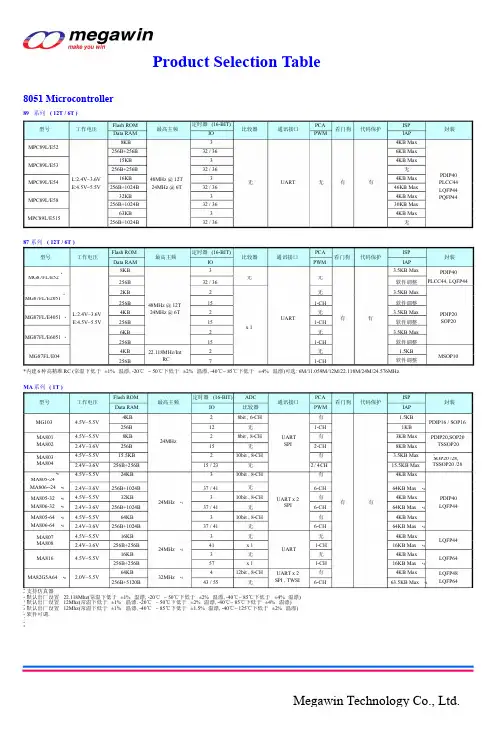
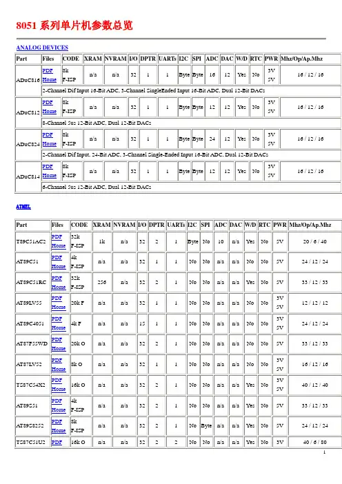
C8051F单片机选型列表
- 格式:pdf
- 大小:63.44 KB
- 文档页数:3
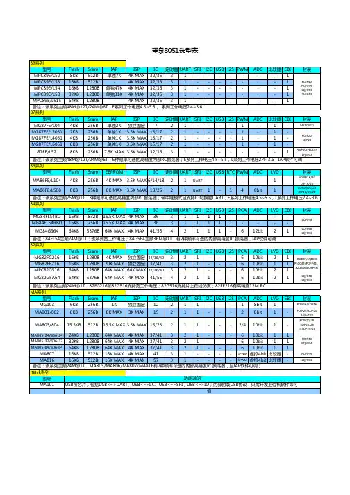
附录3:
部分新型8051兼容单片机性能速查表
在世界上8位单片机诞生后不久,8051的出现了,由于8051在当时8位单片机中的突出性能,它成为事实上的工业标准。
由于Intel公司的技术开放和8051的经典体系结构、良好的兼容性,众多的半导体厂商都热衷于8051及其兼容单片机的发展,特别是近几年来,随着微电子技术与计算机技术的迅猛发展,8051及其兼容单片机的发展日新月异、品种繁多,令人目不暇接。
8051及其兼容单片机的生产厂商各施绝技,生产出各具特色的8051及其兼容单片机,概括说来,新型的8051及其兼容单片机有如下的特点或功能:1.高速度;
2.混合(模拟与数字)信号处理;
3.低功耗;
4.多时钟和实时时钟;
5.大容量存储器;
6.大数量的I/O口和多功能、可配置I/O口;
7.基于串口或JTAG结构的在系统调试;
8.多种复位源;
9.片内可编程门阵列和系统可配置;
10.多种串口;
11.DMA功能;
12.USB接口;
13.视频(电视)信号处理与控制;
14.网络接口;
……
由于与8051兼容的单片机品种繁多,限于篇幅,要介绍所有新型的与8051兼容单片机是不可能的,而要重点介绍若干个品种,既有难以取舍的窘迫,又有挂一漏万之嫌。
即使是仅介绍这些新型的单片机的特点,恐怕也难在一本书中叙述清楚。
作者只好把所收集的与8051兼容的单片机及其特点整理成表格,作为附录供大家在开发选型时参考。
应该说明的是,该表格不可能把所有的与8051兼容的单片机都收入到,所列特点也仅仅是概括性的,不可能把所有的技术指标都给列出。
下表列出了与8051兼容的单片机的生产公司、信号及其特点与主要技术指标。
C8051F MCU 之系列仿真器介绍C8051F 单片机是完全集成的混合信号系统级芯片 (SoC ),具有与MCS-51完全兼容的指令内核。
该系列单片机采用流水线处理(pipe line )技术,不再区分时钟周期和机器周期,能在执行指令期间预处理下一条指令, 从而提高了指令执行效率。
大部分C8051F 单片机具备控制系统所需的 模拟和数字外设,包括看门狗、 ADC 、DAC 、电压比较器、电压基准输出、 定时器、PWM 、定时器捕捉和方波输出等,并具备多种总线接口,包括UART 、 SPI 、SMBus (与I2C 兼容)总线以及CAN 总线。
C8051F 系列单片机采用 FLASH ROM 技术,集 成JTAG ,支持在线编程。
本文重点说明一下 C8051F 开发工具的选择及各版本之间的异同, 以方便开发者选购。
下面所说的开发工具,均以原厂Silicon Laboratories (2003 和Cygnal 兼并)公司为主,国内有兼容的开发工具,可以对号入座。
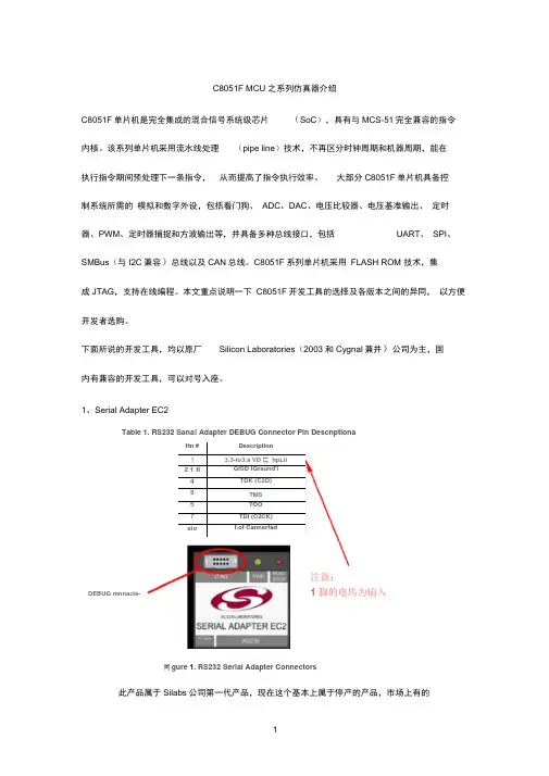
1、Serial Adapter EC2此产品属于Silabs 公司第一代产品,现在这个基本上属于停产的产品,市场上有的Hn # Description 13.3-to3.a VD 匚 hpLii 2 1 fl GlSD fGraund'i 4 TDK (C2D) 5 TMS 5TOO 7TDI (C2CK) aiol\ot Cannsrfad注資:1脚的电馬为输入Table 1. RS232 Sana! Adapter DEBUG Connector Pin DescnptionaDEBUG mnnacla-冋gure 1. RS232 Serial Adapter Connectors话,价格也相对偏高。
不合适!还有一个值得提醒大家的是(也是好多朋友问本空间的开发器为什么1脚为NC ,特做此声明),注意这个DEBUG 的调试接口的关系,在第一脚3.0 to 3.6 VDC In put ,搞过RS232接口的朋友都应该知道,串行口不能向设备提供大电流电源 的(通常的窃电电路也只是小电流方式 ),所以在官方的开发板上都有如下有这个关系。
改良创新后的51单片机-----C8051FMCS-51单片机及其衍生产品在我国乃至世界范围获得了非常广泛的应用,尤其在我国,大部分大专院校都采用MCS-51单片机作为教学机型,大部分单片机系统工程师都熟悉MCS-51单片机。
随着一些髙集成度、髙性能的8位和16位RISC单片机的推出,基于8051内核的单片机正面临着退出市场的境地。
因此一些半导体公司开始对传统8051内核进行大的改造,主要是提高速度和增加片内模拟和数字外设,以期大幅度提高单片机的整体性能.Silabs集成产品公司推出的C8051F单片机是这类MCS-51单片机的典型代表,也是目前功能最全,速度最快的8051衍生单片机。
C8051F单片机的出现令业界人士耳目一新,使广大单片机系统设计人员看到了MCS-51单片机的曙光。
C8051F单片机简介C8051F单片机是完全集成混合信号系统级芯片(SoC),具有与8051兼容的高速CIP-51内核,于MCS-51指令集完全兼容,可以使用标准803×805X汇编器和编译器进行软件开发。
除了具有标准8051的数字外设部件之外,片内还集成了数据采集和控制系统中常用的模拟部件和其它数字外设及功能部件。
这些外设或功能部件包括模拟多路选择器、可编程增益放大器、ADC、DAC、电压比较器、电压基准、温度传感器、SMBUS、12C、UART、SPI、定时器、可编程计数器、定时器阵列(PCA) 、数字I/O端口、电源监视器、看门狗定时器(WDT)和时钟振荡器等。
所有器件都有内置的FLASH程序存储器和256字节的内部RAM,有些器件内部还有位于外部数据存储器空间的RAM,即XRAM。
C8051F单片机的主要特点C8051F单片机中有丰富的模拟和数字资源,并采用了一些在单片机中前所未有的新技术,在CPU内核的内部和外部有几项关键性的改进。
提高了整体性能,更易于在最终使用中使用。
下面对C8051F单片机的主要特点加以介绍。
Rev. 0.4Copyright © 2014 by Silicon LaboratoriesC8051F35x-DKX EVELOPMENT IT SER S UIDE1. Kit ContentsThe C8051F35x-DK Development Kit contains the following items:⏹ C8051F350 Target Board⏹ C8051Fxxx Development Kit Quick-Start Guide ⏹ AC to DC Power Adapter⏹ USB Debug Adapter (USB to Debug Interface)⏹ USB Cable ⏹ CD-ROM2. Hardware Setup using a USB Debug AdapterThe target board is connected to a PC running the Simplicity Studio via the USB Debug Adapter as shown in Figure 1.1. Connect the USB Debug Adapter to the DEBUG connector on the target board with the 10-pin ribbon cable.2. Connect one end of the USB cable to the USB connector on the USB Debug Adapter.3. Connect the other end of the USB cable to a USB Port on the PC.4. Connect the ac/dc power adapter to power jack P1 on the target board.Notes:⏹ Use the Reset button in the IDE to reset the target when connected using a USB Debug Adapter.⏹ Remove power from the target board and the USB Debug Adapter before connecting or disconnecting theribbon cable from the target board. Connecting or disconnecting the cable when the devices have power can damage the device and/or the USB Debug Adapter.Figure 1.Hardware Setup using a USB Debug AdapterPWRP1.6C8051F35x-DK3. Software SetupSimplicity Studio greatly reduces development time and complexity with Silicon Labs EFM32 and 8051 MCU products by providing a high-powered IDE, tools for hardware configuration, and links to helpful resources, all in one place.Once Simplicity Studio is installed, the application itself can be used to install additional software and documentation components to aid in the development and evaluation process.Figure 2.Simplicity StudioThe following Simplicity Studio components are required for the C8051F350 Development Kit:⏹ 8051 Products Part Support ⏹ Simplicity Developer PlatformDownload and install Simplicity Studio from /8bit-software or /simplicity-studio .Once installed, run Simplicity Studio by selecting Start →Silicon Labs →Simplicity Studio →Simplicity Studio from the start menu or clicking the Simplicity Studio shortcut on the desktop. Follow the instructions to install the software and click Simplicity IDE to launch the IDE.The first time the project creation wizard runs, the Setup Environment wizard will guide the user through the process of configuring the build tools and SDK selection.In the Part Selection step of the wizard, select from the list of installed parts only the parts to use during development. Choosing parts and families in this step affects the displayed or filtered parts in the later device selection menus. Choose the C8051F35x family by checking the C8051F35x check box. Modify the part selection at any time by accessing thePart Management dialog from the Window →Preferences →Simplicity Studio →Part Management menu item.Simplicity Studio can detect if certain toolchains are not activated. If the Licensing Helper is displayed after completing the Setup Environment wizard, follow the instructions to activate the toolchain.C8051F35x-DK3.1. Running BlinkyEach project has its own source files, target configuration, SDK configuration, and build configurations such as the Debug and Release build configurations. The IDE can be used to manage multiple projects in a collection called a workspace. Workspace settings are applied globally to all projects within the workspace. This can include settings such as key bindings, window preferences, and code style and formatting options. Project actions, such as build and debug are context sensitive. For example, the user must select a project in the Project Explorer view in order to build that project.To create a project based on the Blinky example:1. Click the Software Examples tile from the Simplicity Studio home screen.2. In the Kit drop-down, select C8051F350 Development Kit, in the Part drop-down, select C8051F350, andin the SDK drop-down, select the desired SDK. Click Next.3. Under C8051F350 Development Kit, select F35x Blinky, click Next, and click Finish.4. Click on the project in the Project Explorer and click Build, the hammer icon in the top bar. Alternatively,go to Project→Build Project.5. Click Debug to download the project to the hardware and start a debug session.button to start the code running. The LED should blink.6. Press the Resume7. Press the Suspendbutton to stop the code.8. Press the Reset the device button to reset the target MCU.button to return to the development perspective.9. Press the Disconnect3.2. Simplicity Studio HelpSimplicity Studio includes detailed help information and device documentation within the tool. The help contains descriptions for each dialog window. To view the documentation for a dialog, click the question mark icon in thewindow:This will open a pane specific to the dialog with additional details.The documentation within the tool can also be viewed by going to Help→Help Contents or Help→Search.C8051F35x-DK4. Target BoardThe C8051F35x Development Kit includes a target board with a C8051F350 device pre-installed for evaluation and preliminary software development. Numerous input/output (I/O) connections are provided to facilitate prototyping using the target board. Refer to Figure3 for the locations of the various I/O connectors.P1Power connector (accepts input from 7 to 15 VDC unregulated power adapter)J122-pin Expansion I/O connectorJ3Port I/O Configuration Jumper BlockJ4DEBUG connector for Debug Adapter interfaceJ5DB-9 connector for UART0 RS232 interfaceJ6Analog I/O terminal blockJ7Connector for IDAC0 voltage circuitJ8USB Debug Adapter target board power connectorJ9, J10External crystal enable connectorsJ11Connector for IDAC1 voltage circuitJ12Connector block for Thermistor circuitryJ13, J14ADC external voltage reference connectorsFigure3.C8051F350 Target BoardC8051F35x-DK4.1. System Clock SourcesThe C8051F350 device installed on the target board features a calibrated programmable internal oscillator which is enabled as the system clock source on reset. After reset, the internal oscillator operates at a frequency of 3.0625MHz (±2%) by default but may be configured by software to operate at other frequencies. Therefore, in many applications an external oscillator is not required. However, if you wish to operate the C8051F350 device at a frequency not available with the internal oscillator, an external crystal may be used. Refer to the C8051F35x data sheet for more information on configuring the system clock source.The target board is designed to facilitate the installation of an external crystal. Remove shorting blocks at headers J9 and J10 and install the crystal at the pads marked Y1. Install a 10M resistor at R9 and install capacitors at C14 and C15 using values appropriate for the crystal you select. Refer to the C8051F35x data sheet for more information on the use of external oscillators.4.2. Switches and LEDsTwo switches are provided on the target board. Switch SW1 is connected to the RESET pin of the C8051F350. Pressing SW1 puts the device into its hardware-reset state. Switch SW2 is connected to the C8051F350’s general purpose I/O (GPIO) pin through headers. Pressing SW2 generates a logic low signal on the port pin. Remove the shorting block from the jumper to disconnect SW2 from the port pins. The port pin signal is also routed to a pin on the J1 I/O connector. See Table1 for the port pins and headers corresponding to each switch.Three LEDs are also provided on the target board. The red LED labeled PWR is used to indicate a power connection to the target board. The green LEDs labeled with port pin names are connected to the C8051F350’s GPIO pins through headers. Remove the shorting blocks from the headers to disconnect the LEDs from the port pins. The port pin signals are also routed to pins on the J1 I/O connector. See Table1 for the port pins and headers corresponding to each LED.Table 1. Target Board I/O DescriptionsDescription I/O JumperSW1Reset noneSW2P1.0J3[5–6]Green LED D2P0.6J3[1–2]Green LED D1P0.7J3[3–4]Red LED PWR noneC8051F35x-DK4.3. Expansion I/O Connector (J1)The 34-pin Expansion I/O connector J1 provides access to all signal pins of the C8051F350 device. Pins for V DD and GND as well as pins for VDDA and AGND are also available. A small through-hole prototyping area is also provided. All I/O signals routed to connector J1 are also routed to through-hole connection points between J1 and the prototyping area (see Figure3 on page4). Each connection point is labeled indicating the signal available at the connection point. See Table2 for a list of pin descriptions for J1.Table 2. J1 Pin DescriptionsPin #Description Pin #Description Pin #Description1V DD13P1.225AIN32GND14P1.326AIN43P0.015P1.427AIN54P0.116P1.528AIN65P0.217P1.6/IDAC029AIN76P0.318P1.7/IDAC130VREF+7P0.419P2.031/RST8P0.520AGND32VREF–9P0.621AGND33VDDA10P0.722AIN034AGND11P1.023AIN1--P1.124AIN2--4.4. Target Board DEBUG Interface (J4)The DEBUG connector (J4) provides access to the DEBUG (C2) pins of the C8051F350. It is used to connect the Serial Adapter or the USB Debug Adapter to the target board for in-circuit debugging and Flash programming. Table3 shows the DEBUG pin definitions.Table 3. DEBUG Connector Pin DescriptionsPin #Description1+3VD(+3.3VDC)2, 3, 9GND (Ground)4C2D5/RST(Reset)6P3.07C2CK8Not Connected10USB Power4.5. Serial Interface (J5)A RS232 transceiver circuit and DB-9 (J5) connector are provided on the target board to facilitate serial connections to UART0 of the C8051F350. The TX, RX, RTS and CTS signals of UART0 may be connected to the DB-9 connector and transceiver by installing shorting blocks on header J3.J3[7–8]- Install shorting block to connect UART0 TX (P0.4) to transceiver.J3[9–10]- Install shorting block to connect UART0 RX (P0.5) to transceiver.J3[11–12]- Install shorting block to connect UART0 RTS (P1.4) to transceiver.J3[13–14]- Install shorting block to connect UART0 CTS (P1.5) to transceiver.C8051F35x-DK4.6. Analog I/O (J6)Many of the C8051F350 target device’s port pins are connected to the J6 terminal block. Connections for VDDA, AGND, ADC external voltage references, IDAC outputs and ADC inputs are available. Refer to Table4 for the J6 terminal block connections.Table 4. J6 Terminal Block Pin DescriptionsPin #Description Pin #Description1IDAC08AIN32IDAC19AIN43VREF+10AIN54VREF–11AIN65AIN012AIN76AIN113AGND7AIN214VDDA4.7. IDAC Connectors (J7, J11)The C8051F350 target board also features two Current-to-Voltage 1K load resistors that may be connected to the 10-bit current-mode Digital-to-Analog Converters (IDACs) on port pins P1.6 and P1.7. Install a shorting block on J7 to connect the IDAC0/P1.6 pin of the target device to a load resistor. Install a second shorting block on J11 to connect the IDAC1/P1.7 pin of the target device to a load resistor. The IDAC signals are then routed to the J1 and J6 connectors.4.8. USB Debug Adapter Target Board Power Connector (J8)The USB Debug Adapter includes a connection to provide power to the target board. This connection is routed from J4[10] to J8[1]. Place a shorting block at header J8[2-3] to power the board directly from an ac/dc power adapter. Place a shorting block at header J8[1-2] to power the board from the USB Debug Adapter. Please note that the second option is not supported with either the EC1 or EC2 Serial Adapters.4.9. Thermistor Connector Block (J12)A thermistor circuit is included on the board which allows for a ratiometric measurement of the included thermistor. To use the circuit, remove the shorting blocks on the IDAC headers (J7, J11) and the External Voltage Reference headers (J13, J14). Next, connect all of the signals on the thermistor connector block (J12). Software on the chip can be written to use IDAC0 as a reference current source for the circuit. The current creates a voltage across R27 which is used as an external Voltage Reference input, while the voltage across the thermistor (R26) can be measured by connecting AIN0.0 to the AIN+ ADC input, and AIN0.1 to the AIN- ADC input.4.10. External Voltage Reference (J13, J14)A precision 2.5V voltage reference source is also included on the C8051F350 target board. To use this circuit as a reference source for the ADC, place shorting block on headers J13 and J14. Note that software on the device should be configured to use an external reference when using this configuration. When using the internal (on-chip) reference source, headers J13 and J14 should be left open.C8051F35x-DKC8051F35x-DKC8051F35x-DKD OCUMENT C HANGE L ISTRevision 0.1 to Revision 0.2⏹Section 1, added USB Debug Adapter and USBCable.⏹Section 2, changed name from "Hardware Setup" to"Hardware Setup using an EC2 Serial Adapter".⏹Section 2, added 2 Notes bullets.⏹Section 2, removed Note from bottom of page.⏹Added Section 3, "Hardware Setup using a USBDebug Adapter".⏹Section 5.4.2, changed step 2 to include newinstructions.⏹Section 7, J4, changed "Serial Adapter" to "DebugAdapter".⏹Target Board DEBUG Interface Section, added USBDebug Adapter.⏹DEBUG Connector Pin Descriptions Table, changedpin 4 to C2D.⏹Changed "jumper" to "header".⏹EC2 Serial Adapter section, added EC2 to thesection title, table title and figure title.⏹EC2 Serial Adapter section, changed "JTAG" to"DEBUG".⏹Added "USB Debug Adapter" section.⏹Section 7, J8, changed "Serial Adapter" to "USBDebug Adapter"⏹DEBUG Connector Pin Descriptions Table, changedpin 10 to USB Power⏹USB Debug Adapter Target Board Power Connector(J8) Section, changed "Serial" to "USB Debug" Revision 0.2 to Revision 0.3⏹Removed EC2 Serial Adapter from Kit Contents.⏹Removed Section 2. Hardware Setup using an EC2Serial Adapter. See RS232 Serial Adapter (EC2)User's Guide.⏹Removed Section 8. EC2 Serial Adapter. SeeRS232 Serial Adapter (EC2) User's Guide.⏹Removed Section 9. USB Debug Adapter. See USBDebug Adapter User's Guide.Revision 0.3 to Revision 0.4⏹Updated "Software Setup‚" on page 2.DisclaimerSilicon Laboratories intends to provide customers with the latest, accurate, and in-depth documentation of all peripherals and modules available for system and software implementers using or intending to use the Silicon Laboratories products. Characterization data, available modules and peripherals, memory sizes and memory addresses refer to each specific device, and "Typical" parameters provided can and do vary in different applications. Application examples described herein are for illustrative purposes only. Silicon Laboratories reserves the right to make changes without further notice and limitation to product information, specifications, and descriptions herein, and does not give warranties as to the accuracy or completeness of the included information. Silicon Laboratories shall have no liability for the consequences of use of the information supplied herein. This document does not imply or express copyright licenses granted hereunder to design or fabricate any integrated circuits. The products must not be used within any Life Support System without the specific written consent of Silicon Laboratories. A "Life Support System" is any product or system intended to support or sustain life and/or health, which, if it fails, can be reasonably expected to result in significant personal injury or death. Silicon Laboratories products are generally not intended for military applications. Silicon Laboratories products shall under no circumstances be used in weapons of mass destruction including (but not limited to) nuclear, biological or chemical weapons, or missiles capable of delivering such weapons.Trademark InformationSilicon Laboratories Inc., Silicon Laboratories, Silicon Labs, SiLabs and the Silicon Labs logo, CMEMS®, EFM, EFM32, EFR, Energy Micro, Energy Micro logo and combinations thereof, "the world’s most energy friendly microcontrollers", Ember®, EZLink®, EZMac®, EZRadio®, EZRadioPRO®, DSPLL®, ISOmodem ®, Precision32®, ProSLIC®, SiPHY®, USBXpress® and others are trademarks or registered trademarks of Silicon Laboratories Inc. ARM, CORTEX, Cortex-M3 and THUMB are trademarks or registered trademarks of ARM Holdings. Keil is a registered trademark of ARM Limited. All other products or brand names mentioned herein are trademarks of their respective holders. Silicon Laboratories Inc.400 West Cesar ChavezAustin, TX 78701USAIoT Portfolio/IoT SW/HW /simplicity Quality /quality Support and Community 。
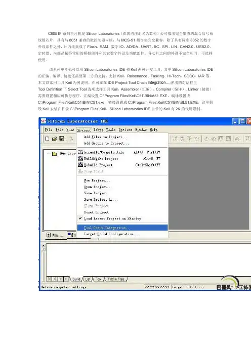
C8051F系列单片机是Silicon Laboratories(在国内注册名为芯科)公司推出完全集成的混合信号系统级芯片,具有与8051兼容的微控制器内核,与MCS-51 指令集完全兼容。
除了具有标准8052的数字外设部件之外,片内还集成了Flash、RAM、数字IO、AD/DA、UART、IIC、SPI、LIN、CAN2.0、USB2.0、定时器、内部晶振等常用的模拟部件和其它数字外设及功能部件。
各芯片之间的外设不完全相同,可选择使用。
该系列单片机可以用Silicon Laboratories IDE和Keil两种开发工具。
其中Silicon Laboratories IDE 的汇编、编译、链接还需要第三方的支持,支持Keil、Raisonance、Tasking、Hi-Tech、SDCC、IAR等。
本文以常用工具Keil为例说明。
在可在在IDE Project-Tool Chain Integration…,弹出的对话框里Tool Definition下Select Tool选项选择工具Keil,Assembler(汇编)、Compiler(编译)、Linker(链接)需要设置相应可执行程序,汇编设置C:\Program Files\Keil\C51\BIN\A51.EXE,编译设置成C:\Program Files\Keil\C51\BIN\C51.exe,链接设置成C:\Program Files\Keil\C51\BIN\BL51.EXE,这里假设Keil安装在目录C:\Program Files\Keil。
Silicon Laboratories IDE自带的Keil有2K的代码限制。
C8051F支持的适配器有两种,RS232串行适配器和USB调试适配器。
在Silicon Laboratories IDE 中Options-Connection Options…,弹出的对话框有RS232串行适配器和USB调试适配器选项,调试接口有JTAG和C2。
c8051f单片机原理及应用C8051F单片机是由Silicon Laboratories公司推出的一款高性能、低功耗、集成度高的8位单片机系列,它采用了高速8051内核,具有快速的执行速度和高效的计算能力,适用于各种应用领域。
本文将详细介绍C8051F单片机的原理和应用。
一、C8051F单片机原理1.8051内核C8051F单片机采用了高速的8051内核,它包含了一个中央处理器(CPU)、存储器、输入/输出端口、定时器/计数器、串行接口等模块。
8051内核具有简单易学、易于控制和可靠性高等特点,被广泛应用于各种嵌入式系统中。
2.存储器C8051F单片机的存储器包括闪存、RAM和EEPROM。
其中,闪存用于存储程序代码,RAM用于存储数据,EEPROM用于存储非易失性数据。
C8051F单片机的存储器容量从4KB到128KB不等,可以满足不同应用的需求。
3.输入/输出端口C8051F单片机的输入/输出端口包括数字输入/输出端口和模拟输入/输出端口。
数字输入/输出端口用于连接数字设备,模拟输入/输出端口用于连接模拟设备。
C8051F单片机的输入/输出端口可以通过软件配置,实现各种功能。
4.定时器/计数器C8051F单片机的定时器/计数器包括多个独立的定时器和计数器,它们可以通过软件配置,实现各种计时和计数功能。
5.串行接口C8051F单片机的串行接口包括SPI接口、I2C接口和UART接口。
它们可以用于与外部设备进行通信,实现数据交换和控制。
二、C8051F单片机应用C8051F单片机广泛应用于各种嵌入式系统中,例如:工业控制、智能家居、医疗设备、电子仪器等。
1.工业控制C8051F单片机可以用于各种工业控制系统中,如温度控制、湿度控制、压力控制等。
它具有高速的运算能力和丰富的输入/输出端口,可以实现复杂的控制算法和实时控制。
2.智能家居C8051F单片机可以用于智能家居系统中,如智能灯光控制、智能窗帘控制、智能门锁控制等。
C8051F系列MCU CygnalC8051F(已被Silicon Lab收购)系列单片机是真正能独立工作的片上系统SOCCPU有效地管理模拟和数字外设可以关闭单个或全部外设以节省功耗FLASH存储器还具有在系线重新编程的能力即可用作程序存储器又可用作于非易失性数据存储应用程序可以使用MOVC和MOVX指令对FLASH进行读或改写。
一.Cygnal C8051F系列单片机特点 1.片内资源 8~12位多通道ADC 1~2路12位DAC 1~2路电压比较器 内部或外部电压基准 内置温度传感器±3 16位可编程定时/计数器阵列PCA可用于PWM等 3~5个通用16位定时器 8~64个通用I/O口 带有I2C/SMBusSPI1~2个UART多类型串行总线 8~64K Flash存贮器 256~4K数据存贮器RAM 片内时钟源内置电源监测看门狗定时器 2.主要特点 高速的20MIPS~25MIPS与8051全兼容的CIP51内核 内部Flash存贮器可实现在系统编程即可作程序存贮器也可作非易失性数据存贮 工作电压为2.7V~3.6V典型值为3VI/ORSTJTAG引脚均允许5V电压输入 全系列均为工业级芯片-45℃~+85℃ 片内JTAG仿真电路提供全速的电路内仿真,不占用片内用户资源,支持断点单步观察点运行和停止等调试命令支持存贮器和寄存器校验和修改
二.有关C8051F系列 CPU 1.与标准8051完全兼容 Cygnal C8051F系列单片机采用CIP51内核,Cygnal指令与MCS51指令系统全兼容可用标准的ASM51Keil C高级语言开发编译C8051F系列单片机的程序 2.高速指令处理能力 标准的8051一个机器周期要占用12个系统时钟周期执行一条指令最少要一个机器周期CygnalC8051F系列单片机指令处理采用流水线结构机器周期由标准的12个系统时钟周期降为1个系统时钟周期指令处理能力比MCS51大大提高。CIP-51内核70% 指令的执行是在一个或两个系统时钟周期内完成的,只有四条指令的执行需4个以上时钟周期。 CIP-51指令与MCS51指令系统完全兼容,共有111条指令。 3.增加了中断源 标准的8051只有7个中断源,而Cygnal C8051F系列单片机扩展了中断处理,这对于时实多任务系统的处理是很重要的。扩展的中断系统向CIP-51提供22个中断源,允许大量的模拟和数字外设中断。一个中断处理需要较少的CPU干预,却有更高的执行效率。 4.增加了复位源 标准的8051只有外部引脚复位,Cygnal C8051F系列单片机增加了7种复位源,使系统的可靠性大大提高,每个复位源都可以由用户用软件禁止。它的复位源是: 1 片内电源监视 2 WDT看门狗定时器 3 时钟丢失检测器 4 比较器0输出电平检测 5 软件强制复位 6 CNVSTRAD转换启动 7 外部引脚RST复位可双向复位 8 提供内部时钟源 标准的8051只有外部时钟,Cygnal C8051F系列单片机有内部独立的时钟源。C8051F300/F302提供的内部时钟误差在2%以内,在系统复位后默认内部时钟。如果需要,可接外部时钟并可在程序运行时实现内外部时钟之间的切换。外部时钟可以是晶体RCC或外部时钟脉冲,以上的功能在低功耗应用系统中非常有用。
Effective Date:Bulletin Issue Date:Jan 11, 2023Jan 11, 2023Description of ChangeSilicon Labs is pleased to announce the release of datasheet version 1.3 for the C8051F50x/51x devices.The datasheet has been updated to add a separate table (Table 2.2) for Not Recommended for New Designs (NRND) devices.Link to the datasheet:https:///documents/public/data-sheets/C8051F50x-51x.pdf 2301111412 C8051F50x/51x v1.3 Datasheet UpdateProduct IdentificationExisting Part #C8051F500-AMC8051F500-AMRC8051F500-AQC8051F500-AQRC8051F500-IM C8051F500-IMRC8051F500-IQC8051F500-IQRC8051F501-AMC8051F501-AMRC8051F501-AQC8051F501-AQRC8051F501-IMC8051F501-IMRC8051F501-IQC8051F501-IQRC8051F502-AMC8051F502-AMRC8051F502-AQC8051F502-AQRC8051F502-IMC8051F502-IMRC8051F502-IQC8051F502-IQRC8051F503-AMC8051F503-AMRC8051F503-AQC8051F503-AQRC8051F503-IMC8051F503-IMRC8051F503-IQC8051F503-IQRC8051F504-AMC8051F504-AMRC8051F504-AQC8051F504-AQRC8051F504-IMC8051F504-IMRC8051F504-IQReason for ChangeUpdates to the Product Selection Guide.Kit IdentificationThis change is considered a minor change which does not affect form, fit, function, quality, or reliability. The information is being provided as a customer courtesy.Please contact your local Silicon Labs sales representative with any questions about this notification. A list of Silicon Labs sales representatives may be found at .Customer Actions Needed:Review updated datasheet.User RegistrationRegister today to create your account on . Your personalized profile allows you to receive technical document updates, new product announcements, “how-to” and design documents, product change notices (PCN) and other valuable content available only to registered users. /profileSilicon Laboratories Inc.400 West Cesar ChavezAustin, TX 78701 DisclaimerSilicon Labs intends to provide customers with the latest, accurate, and in-depth documentation of all peripherals and modules available for system and software implementers using or intending to use the Silicon Labs products. Characterization data, available modules andperipherals, memory sizes and memory addresses refer to each specific device, and "Typical" parameters provided can and do vary in different applications. Application examples described herein are for illustrative purposes only. Silicon Labs reserves the right to make changes without further notice and limitation to product information, specifications, and descriptions herein, and does not give warranties as to the accuracy or completeness of the included information. Silicon Labs shall have no liability for the consequences of use of the information supplied herein. This document does not imply or express copyright licenses granted hereunder to design or fabricate any integrated circuits. The products are not designed or authorized to be used within any Life Support System without the specific written consent of Silicon Labs. A "Life Support System" is any product or system intended to support or sustain life and/or health, which, if it fails, can be reasonably expected to result in significant personal injury or death. Silicon Labs products are not designed or authorized for military applications. Silicon Labs products shall under no circumstances be used in weapons of mass destruction including (but not limited to) nuclear, biological or chemical weapons, or missiles capable of delivering such weapons.Trademark InformationSilicon Laboratories Inc.® , Silicon Laboratories®, Silicon Labs®, SiLabs® and the Silicon Labs logo®, Bluegiga®, Bluegiga Logo®,Clockbuilder®, CMEMS®, DSPLL®, EFM®, EFM32®, EFR, Ember®, Energy Micro, Energy Micro logo and combinations thereof, "the world’s most energy friendly microcontrollers", Ember®, EZLink®, EZRadio®, EZRadioPRO®, Gecko®, ISOmodem®, Micrium, Precision32®, ProSLIC®, Simplicity Studio®, SiPHY®, Telegesis, the Telegesis Logo®, USBXpress®, Zentri and others are trademarks or registered trademarks of Silicon Labs. ARM, CORTEX, Cortex-M3 and THUMB are trademarks or registered trademarks of ARM Holdings. Keil is aregistered trademark of ARM Limited. All other products or brand names mentioned herein are trademarks of their respective holders.。