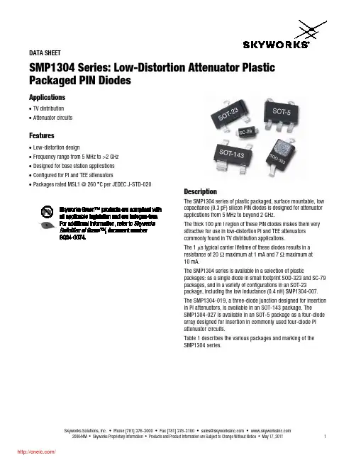
DATA SHEETSMP1304 Series: Low-Distortion Attenuator Plastic Packaged PIN DiodesApplications•TV distribution•Attenuator circuitsFeatures•Low-distortion design•Frequency range from 5 MHz to >2 GHz•Designed for base station applications•Configured for PI and TEE attenuators•Packages rated MSL1 @ 260°C per JEDEC J-STD-020DescriptionThe SMP1304series of plastic packaged, surface mountable, lowcapacitance (0.3 pF) silicon PIN diodes is designed for attenuatorapplications from 5 MHz to beyond 2 GHz.The thick 100 μm I region of these PIN diodes makes them veryattractive for use in low-distortion PI and TEE attenuatorscommonly found in TV distribution applications.The 1 μs typical carrier lifetime of these diodes results in aresistance of 20 Ωmaximum at 1 mA and 7 Ωmaximum at10 mA.The SMP1304series is available in a selection of plasticpackages: as a single diode in small footprint SOD-323 and SC-79package s, and in a variety of configurations in an SOT-23package, including the low inductance (0.4 nH) SMP1304-007.The SMP1304-019, a three-diode junction designed for insertionin PI attenuators, is available in an SOT-143 package. TheSMP1304-027 is available in an SOT-5 package as a four-diodearray designed for insertion in commonly used four-diode PIattenuator circuits.Table 1 describes the various packages and marking of theSMP1304 series.Skyworks Solutions, Inc. • Phone [781] 376-3000• Fax [781] 376-3100 • sales@ • 200044M• Skyworks Proprietary I nformation • Products and Product Information are Subject to Change Without Notice • May 17, 20111DATA SHEET • SMP1304 SERIESSkyworks Solutions, Inc. • Phone [781] 376-3000 • Fax [781] 376-3100 • sales@ • 2May 17, 2011 • Skyworks Proprietary I nformation • Products and Product Information are Subject to Change Without Notice • 200044M(Sn/Pb) packaging is not recommended for new designs .Innovation to Go™Select Linear Products (indicated by ♦) now available for purchase online.SMP1304-007The inductance of the SMP1304-007 is effectively reduced to 0.4 nH compared to the 1.5 nH of the standard configuration. The lower inductance is particularly beneficial when the diodes are used as shunt -connected switches at frequencies >500 MHz where inductance is the primary limitation on maximum switch isolation.To achieve the effective 0.4 nH, the SMP1304-007 must be inserted in the microstrip circuit board with a gap in the trace as shown in Figure 1. Because of the polarity of the diode junction, the low inductance can only be achieved with the cathode connected to ground.Figure 1. SOT-23 Package Trace GapFigure 2. SMP1304-019 Package (PI)SMP1304-019 PI Attenuator PIN DiodesThe SMP1304-019 uses three PIN diode junctions in an SOT -143 package (see Figure 2). The junctions are configured for ease ofinsertion in PI attenuator circuits in common use from 10 MHz to >1 GHz. The SMP1304-019 PIN diode junction was designed for low capacitance, a wide resistance dynamic range, and low distortion performance.Electrical and Mechanical SpecificationsThe absolute maximum ratings of the SMP1304 series are provided in Table 2. Electrical specifications are provided in Table 3. Resistance versus temperature measurements are provided in Table 4.Typical performance characteristics of the SMP1304 series are illustrated in Figures 3 to 6. Package dimensions are shown in Figures 7 to 15 (odd numbers), and tape and reel dimensions are provided in Figures 8 to 16 (even numbers).Package and Handling InformationInstructions on the shipping container label regarding exposure to moisture after the container seal is broken must be followed. Otherwise, problems related to moisture absorption may occur when the part is subjected to high temperature during solder assembly.The SMP1304 series is rated to Moisture Sensitivity Level 1 (MSL1) at 260 °C. It can be used for lead or lead -free soldering. For additional information, refer to the Skyworks Application Note, Solder Reflow Information , document number 200164 Care must be taken when attaching this product, whether it is done manually or in a production solder reflow environment. Production quantities of this product are shipped in a standard tape and reel format.DA TA SHEET • SMP1304 SERIESNote:Exposure to maximum rating conditions for extended periods may reduce device reliability. There is no damage to device with only one parameter set at the limit and all other parameters set at or below their nominal value. Exceeding any of the limits listed here may result in permanent damage to the device.CAUTION: Although this device is designed to be as robust as possible, Electrostatic Discharge (ESD) can damage this device. This device must be protected at all times from ESD. Static charges may easily produce potentials of several kilovolts on the human body or equipment, which can discharge without detection. Industry-standard ESD precautions should be used at all times. TheSMP1304 series PIN diodes are Class 1C ESD devices.Table 3. SMP1304 Series Electrical Specifications (Note 1)Note 1:Performance is guaranteed only under the conditions listed in this Table.Note 2:The SMP1304-019 and SMP1304-027 maximum capacitance is 0.45 pF.Skyworks Solutions, Inc. • Phone [781] 376-3000 • Fax [781] 376-3100 • sales@ • 200044M• Skyworks Proprietary I nformation • Products and Product Information are Subject to Change Without Notice • May 17, 20113DATA SHEET • SMP1304 SERIESSkyworks Solutions, Inc. • Phone [781] 376-3000 • Fax [781] 376-3100 • sales@ • 4May 17, 2011 • Skyworks Proprietary I nformation • Products and Product Information are Subject to Change Without Notice • 200044MTypical Performance CharacteristicsFigure 3. Series Resistance vs Current @ 100 MHzFigure 5. Capacitance vs Reverse VoltageFigure 4. DC CharacteristicFigure 6. Conductance vs Frequency and Reverse VoltageDA TA SHEET • SMP1304 SERIESSkyworks Solutions, Inc. • Phone [781] 376-3000 • Fax [781] 376-3100 • sales@ • 200044M • Skyworks Proprietary I nformation • Products and Product Information are Subject to Change Without Notice • May 17, 20115Figure 7. SC-79 Package Dimension DrawingFigure 8. SC-79 Tape and Reel DimensionsDATA SHEET • SMP1304 SERIESSkyworks Solutions, Inc. • Phone [781] 376-3000 • Fax [781] 376-3100 • sales@ • 6May 17, 2011 • Skyworks Proprietary I nformation • Products and Product Information are Subject to Change Without Notice • 200044MFigure 9. SOD-323 Package Dimension DrawingFigure 10. SOD-323 Tape and Reel DimensionsDA TA SHEET • SMP1304 SERIESSkyworks Solutions, Inc. • Phone [781] 376-3000 • Fax [781] 376-3100 • sales@ • 200044M • Skyworks Proprietary I nformation • Products and Product Information are Subject to Change Without Notice • May 17, 20117Figure 11. SOT-5 Package Dimension DrawingFigure 12. SOT-5 Tape and Reel DimensionsDATA SHEET • SMP1304 SERIESSkyworks Solutions, Inc. • Phone [781] 376-3000 • Fax [781] 376-3100 • sales@ • 8May 17, 2011 • Skyworks Proprietary I nformation • Products and Product Information are Subject to Change Without Notice • 200044MFigure 13. SOT-23 Package Dimension DrawingFigure 14. SOT-23 Tape and Reel DimensionsDA TA SHEET • SMP1304 SERIESSkyworks Solutions, Inc. • Phone [781] 376-3000 • Fax [781] 376-3100 • sales@ • 200044M • Skyworks Proprietary I nformation • Products and Product Information are Subject to Change Without Notice • May 17, 20119Figure 15. SOT-143 Package Dimension DrawingFigure 16. SOT-143 Tape and Reel DimensionsDATA SHEET • SMP1304 SERIESSkyworks Solutions, Inc. • Phone [781] 376-3000 • Fax [781] 376-3100 • sales@ • 10May 17, 2011 • Skyworks Proprietary I nformation • Products and Product Information are Subject to Change Without Notice • 200044MCopyright © 2002-2007, 2009, 2010, 2011 Skyworks Solutions, Inc. All Rights Reserved.Information in this document is provided in connection with Skyworks Solutions, Inc. (“Skyworks”) products or services. These materials, including the information contained herein, are provided by Skyworks as a service to its customers and may be used for informational purposes only by the customer. Skyworks assumes no responsibility for errors or omissions in these materials or the information contained herein. Skyworks may change its documentation, products, services, specifications or product descriptions at any time, without notice. Skyworks makes no commitment to update the materials or information and shall have no responsibility whatsoever for conflicts, incompatibilities, or other difficulties arising from any future changes.No license, whether express, implied, by estoppel or otherwise, is granted to any intellectual property rights by this document. Skyworks assumes no liability for any materials, products orinformation provided hereunder, including the sale, distribution, reproduction or use of Skyworks products, information or materials, except as may be provided in Skyworks Terms and Conditions of Sale.THE MATERIALS, PRODUCTS AND INFORMATION ARE PROVIDED “AS IS” WITHOUT WARRANTY OF ANY KIND, WHETHER EXPRESS, IMPLIED, STATUTORY, OR OTHERWISE, INCLUDING FITNESS FOR A PARTICULAR PURPOSE OR USE, MERCHANTABILITY, PERFORMANCE, QUALITY OR NON -INFRINGEMENT OF ANY INTELLECTUAL PROPERTY RIGHT; ALL SUCH WARRANTIES ARE HEREBY EXPRESSLY DISCLAIMED. SKYWORKS DOES NOT WARRANT THE ACCURACY OR COMPLETENESS OF THE INFORMATION, TEXT, GRAPHICS OR OTHER ITEMS CONTAINED WITHIN THESE MATERIALS. SKYWORKS SHALL NOT BE LIABLE FOR ANY DAMAGES, INCLUDING BUT NOT LIMITED TO ANY SPECIAL, INDIRECT, INCIDENTAL, STATUTORY, OR CONSEQUENTIAL DAMAGES, INCLUDING WITHOUT LIMITATION, LOST REVENUES OR LOST PROFITS THAT MAY RESULT FROM THE USE OF THE MATERIALS OR INFORMATION, WHETHER OR NOT THE RECIPIENT OF MATERIALS HAS BEEN ADVISED OF THE POSSIBILITY OF SUCH DAMAGE.Skyworks products are not intended for use in medical, lifesaving or life -sustaining applications, or other equipment in which the failure of the Skyworks products could lead to personal injury, death, physical or environmental damage. Skyworks customers using or selling Skyworks products for use in such applications do so at their own risk and agree to fully indemnify Skyworks for any damages resulting from such improper use or sale.Customers are responsible for their products and applications using Skyworks products, which may deviate from published specifications as a result of design defects, errors, or operati on ofproducts outside of published parameters or design specifications. Customers should include design and operating safeguards to minimize these and other risks. Skyworks assumes no liability for applications assistance, customer product design, or damage to any equipment resulting from the use of Skyworks products outside of stated published specifications or parameters.Skyworks, the Skyworks symbol, and “Breakthrough Simplicity” are trademarks or registered trademarks of Skyworks Solutions, Inc., in the United States and other countries. Third -party brands and names are for identification purposes only, and are the property of their respective owners. Additional information, including relevant terms and conditions, posted at , are incorporated by reference.分销商库存信息:SKYWORKS-SOLUTIONSSMP1304-004LF SMP1304-027LF。