语音芯片TLV320AIC23使用
- 格式:ppt
- 大小:1.92 MB
- 文档页数:25

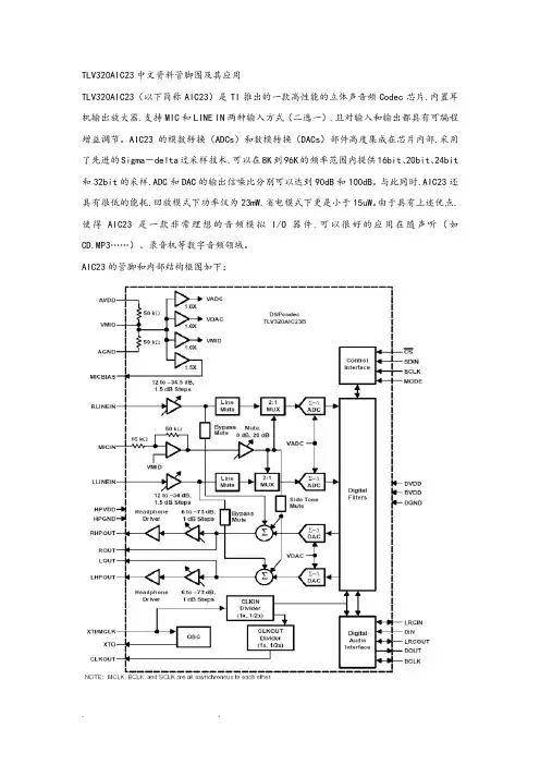
TLV320AIC23中文资料管脚图及其应用TLV320AIC23(以下简称AIC23)是TI推出的一款高性能的立体声音频Codec芯片.内置耳机输出放大器.支持MIC和LINE IN两种输入方式(二选一).且对输入和输出都具有可编程增益调节。
AIC23的模数转换(ADCs)和数模转换(DACs)部件高度集成在芯片内部.采用了先进的Sigma-delta过采样技术.可以在8K到96K的频率范围内提供16bit、20bit、24bit 和32bit的采样.ADC和DAC的输出信噪比分别可以达到90dB和100dB。
与此同时.AIC23还具有很低的能耗.回放模式下功率仅为23mW.省电模式下更是小于15uW。
由于具有上述优点.使得AIC23是一款非常理想的音频模拟I/O器件.可以很好的应用在随声听(如CD.MP3……)、录音机等数字音频领域。
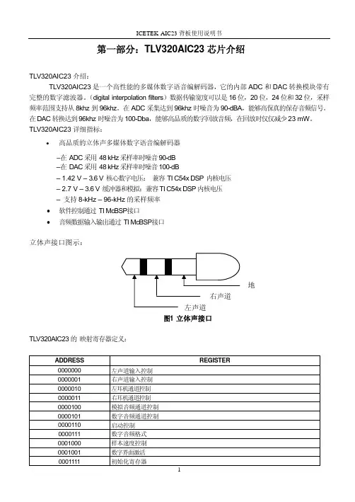
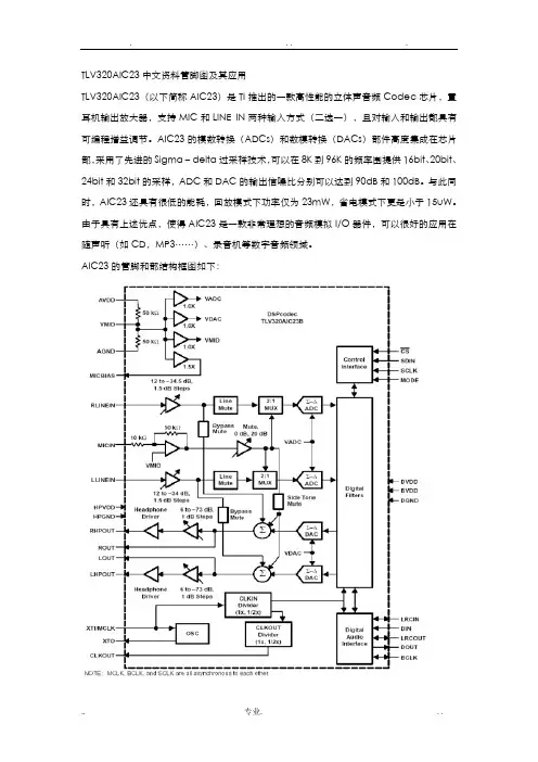
AIC23的管脚和内部结构框图如下:从上图可以看出.AIC23主要的外围接口分为以下几个部分:一.数字音频接口:主要管脚为BCLK-数字音频接口时钟信号(bit时钟).当AIC23为从模式时(通常情况).该时钟由DSP 产生;AIC23为主模式时.该时钟由AIC23产生;LRCIN-数字音频接口DAC方向的帧信号(I2S模式下word时钟)LRCOUT-数字音频接口ADC方向的帧信号DIN-数字音频接口DAC方向的数据输入DOUT-数字音频接口ADC方向的数据输出这部分可以和DSP的McBSP(Multi-channel buffered serial port.多通道缓存串口)无缝连接.唯一要注意的地方是McBSP的接收时钟和AIC23的BCLK都由McBSP的发送时钟提供.连接示意图如下:二.麦克风输入接口:主要管脚为MICBIAS-提供麦克风偏压.通常是3/4 AVDDMICIN-麦克风输入.由AIC结构框图可以看出放大器默认是5倍增益连接示意图如下:三. LINE IN输入接口:主要管脚为LLINEIN-左声道LINE IN输入RLINEIN-右声道LINE IN输入连接示意图如下:四.耳机输出接口:主要管脚为LHPOUT-左声道耳机放大输出RHPOUT-右声道耳机放大输出LOUT-左声道输出ROUT-右声道输出从框图可以看出.LOUT和ROUT没有经过内部放大器.所以设计中常用LHPOUT和RHPOUT.连接示意图如下:五.配置接口:主要管脚为SDIN-配置数据输入SCLK-配置时钟DSP通过该部分配置AIC23的内部寄存器.每个word的前7bit为寄存器地址.后9bit为寄存器内容。

TLV320AIC23中文资料管脚图及其应用TLV320AIC23(以下简称AIC23)是TI推出的一款高性能的立体声音频Codec芯片,置耳机输出放大器,支持MIC和LINE IN两种输入方式(二选一),且对输入和输出都具有可编程增益调节。
AIC23的模数转换(ADCs)和数模转换(DACs)部件高度集成在芯片部,采用了先进的Sigma-delta过采样技术,可以在8K到96K的频率围提供16bit、20bit、24bit和32bit的采样,ADC和DAC的输出信噪比分别可以达到90dB和100dB。
与此同时,AIC23还具有很低的能耗,回放模式下功率仅为23mW,省电模式下更是小于15uW。
由于具有上述优点,使得AIC23是一款非常理想的音频模拟I/O器件,可以很好的应用在随声听(如CD,MP3……)、录音机等数字音频领域。
AIC23的管脚和部结构框图如下:从上图可以看出,AIC23主要的外围接口分为以下几个部分:一.数字音频接口:主要管脚为BCLK-数字音频接口时钟信号(bit时钟),当AIC23为从模式时(通常情况),该时钟由DSP产生;AIC23为主模式时,该时钟由AIC23产生;LRCIN-数字音频接口DAC方向的帧信号(I2S模式下word时钟)LRCOUT-数字音频接口ADC方向的帧信号DIN-数字音频接口DAC方向的数据输入DOUT-数字音频接口ADC方向的数据输出这部分可以和DSP的McBSP(Multi-channel buffered serial port,多通道缓存串口)无缝连接,唯一要注意的地方是McBSP的接收时钟和AIC23的BCLK都由McBSP的发送时钟提供,连接示意图如下:二.麦克风输入接口:主要管脚为MICBIAS-提供麦克风偏压,通常是3/4 AVDDMICIN-麦克风输入,由AIC结构框图可以看出放大器默认是5倍增益连接示意图如下:三.LINE IN输入接口:主要管脚为LLINEIN-左声道LINE IN输入RLINEIN-右声道LINE IN输入连接示意图如下:四.耳机输出接口:主要管脚为LHPOUT-左声道耳机放大输出RHPOUT-右声道耳机放大输出LOUT-左声道输出ROUT-右声道输出从框图可以看出,LOUT和ROUT没有经过部放大器,所以设计中常用LHPOUT和RHPOUT,连接示意图如下:五.配置接口:主要管脚为SDIN-配置数据输入SCLK-配置时钟DSP通过该部分配置AIC23的部寄存器,每个word的前7bit为寄存器地址,后9bit为寄存器容。
1 TLV320AIC23语音系统的设计任务及目的1.1 TLV320AIC23语音系统的设计任务课程设计是实践教学环节。
学生通过动手做软件和硬件设计,能够熟练掌握数字信号处理技术,增加对基础知识的消化和理解。
1.2 TLV320AIC23语音系统的设计目的(1)完成硬件设计;(2)完成TLV320AIC23的初始化;(3)进行语音信号的采集与播放。
1.3 TLV320AIC23语音系统介绍在当今的数字化时代背景下,DSP已成为通信、计算机、消费类电子产品等领域的基础器件,是集成电路中发展最快的电子产品,并成为电子产品更新换代的决定因素。
DSP芯片已经被广泛地应用于当今技术革命的各个领域,而且DSP技术也正以极快的速度被应用在通信、电子系统、信号处理系统等许多领域中。
基于TMS320C5509DSP芯片的语音分析器的设计系统的主要功能对语音信号进行采样滤波后FFT变换,然后观察其频谱分布。
通过该分析器可观察到语音信号频谱特征的观察,从而为语音的编解码,压缩,解压缩,语音编码,语音识别语音合成,语音增强等实时语音处理方法的实现及参数的选取提供依据。
本系统是一个数字信号处理系统,是电子技术、信号处理技术与计算技术相结合的产物,也是一个软硬件结合的系统。
2 语音系统的技术方案及硬件电路设计2.1 语音系统的性能指标2.1.1本设计实现的语音系统具有如下主要性能:(1)由于语音信号的频率范围为300Hz-3400Hz(人说话声音)或20Hz-20kHz(音乐,占音频信号全频率),根据采样定理,为保证信息不失真,确定系统的采样频率为8KHz 或96kHz;(2)结合系统采用的TMS320C5509芯片处理速度以及信号采样频率的要求,采用TLV320AIC23DSP芯片作为系统的A/D转换芯片;2.1.2语音系统具有如下优点:(1)音频数据占用资源少(2)音质通信级高(3)开发难度低(4)语音芯片与DSP 接口电路简单(5)体积小2.2硬件设计方案系统框图如图1所示,音源(如麦克风)发出的音频信号经音频处理器的A/D部分转换为数字信号后进人DSP,完成数据的采集工作,由系统的模式识别部分决定对采集的数据进行何种处理(如滤波等),处理后的信号再通过音频编解码器的D/A部分还原为模拟的声音信号送往扬声器输出。
TLV320AIC23中文资料管脚图及其应用TLV320AIC23(以下简称AIC23)是TI推出的一款高性能的立体声音频Codec芯片,内置耳机输出放大器,支持MIC和LINE IN两种输入方式(二选一),且对输入和输出都具有可编程增益调节。
AIC23的模数转换(ADCs)和数模转换(DACs)部件高度集成在芯片内部,采用了先进的Sigma-delta过采样技术,可以在8K到96K的频率范围内提供16bit、20bit、24bit和32bit的采样,ADC和DAC的输出信噪比分别可以达到90dB和100dB。
与此同时,AIC23还具有很低的能耗,回放模式下功率仅为23mW,省电模式下更是小于15uW。
由于具有上述优点,使得AIC23是一款非常理想的音频模拟I/O器件,可以很好的应用在随声听(如CD,MP3……)、录音机等数字音频领域。
AIC23的管脚和内部结构框图如下:从上图可以看出,AIC23主要的外围接口分为以下几个部分:一.数字音频接口:主要管脚为BCLK-数字音频接口时钟信号(bit时钟),当AIC23为从模式时(通常情况),该时钟由DSP产生;AIC23为主模式时,该时钟由AIC23产生;LRCIN-数字音频接口DAC方向的帧信号(I2S模式下word时钟)LRCOUT-数字音频接口ADC方向的帧信号DIN-数字音频接口DAC方向的数据输入DOUT-数字音频接口ADC方向的数据输出这部分可以和DSP的McBSP(Multi-channel buffered serial port,多通道缓存串口)无缝连接,唯一要注意的地方是McBSP的接收时钟和AIC23的BCLK都由McBSP的发送时钟提供,连接示意图如下:二.麦克风输入接口:主要管脚为MICBIAS-提供麦克风偏压,通常是3/4 AVDDMICIN-麦克风输入,由AIC结构框图可以看出放大器默认是5倍增益连接示意图如下:三.LINE IN输入接口:主要管脚为LLINEIN-左声道LINE IN输入RLINEIN-右声道LINE IN输入连接示意图如下:四.耳机输出接口:主要管脚为LHPOUT-左声道耳机放大输出RHPOUT-右声道耳机放大输出LOUT-左声道输出ROUT-右声道输出从框图可以看出,LOUT和ROUT没有经过内部放大器,所以设计中常用LHPOUT和RHPOUT,连接示意图如下:五.配置接口:主要管脚为SDIN-配置数据输入SCLK-配置时钟DSP通过该部分配置AIC23的内部寄存器,每个word的前7bit为寄存器地址,后9bit 为寄存器内容。
1SLEA037A–June 2004–Revised June 2020Submit Documentation FeedbackCopyright ©2004–2020,Texas Instruments IncorporatedDynamic Behavior of the TLV320DAC23and the TLV320AIC23BApplication ReportSLEA037A–June 2004–Revised June 2020Dynamic Behavior of the TLV320DAC23and theTLV320AIC23BKeith Engler,Luis Fernando RodruguezABSTRACTThis application report discusses the following topics:1.The operation based on various settings of the power-down control register.2.The time it takes to be stable after returning from a power-down control command.3.A list of power sequence restrictions.4.The results of changing the external capacitors on VMID.5.IIC communication6.How the sample rate varies proportionally with a change in MCLK while the DAC is in master mode.DISCLAIMER:The information contained in this document is based on lab evaluations using alimited supply of samples.This document is not intended to replace the TLV320DAC23or TLV320AIC23B data manuals or is it in anyway a device specification.Values in thisdocument are not assured for every TLV320DAC23or TLV320AIC23B device.If there are any discrepancies between this document and the data manual,the data manual will prevail.Contents1Power-Down Control Settings ..............................................................................................22Noise Fixed by Toggling Bit D7of Power-Down Control ..............................................................33Power-Up Stability Time ....................................................................................................34Power Sequence .............................................................................................................45VMID Capacitor Variations .................................................................................................56TLV320DAC23IIC Communication (67)Sample Variance With MCLK Changes ...................................................................................6List of Figures1Theoretical Low-Frequency Attenuation (5)List of Tables1Reduction in Power Consumption Results (42)Sample Rates (7)TrademarksAll trademarks are the property of their respective owners.Power-Down Control Settings 2SLEA037A–June 2004–Revised June 2020Submit Documentation FeedbackCopyright ©2004–2020,Texas Instruments IncorporatedDynamic Behavior of the TLV320DAC23and the TLV320AIC23B1Power-Down Control SettingsThere are various software programmable modes to conserve power.See the power-down control register address 0000110section in the data manual for more clarification.Described below is each bit of this register and how each bit responds to being toggled.1.1D0Line InputFunction:Powers down both line inputs.Effect:Can be done dynamically without any audible effects on the DAC or line outputs.1.2D3DACFunction:Powers down both the DAC and DAC filters.Effect:If done dynamically,audible pops and clicks on the DAC.Solution:SoftMute the DAC bit D3register 0000101.Deselect the DAC bit D4register 0000100.Power down the DAC.1.3D4OUTFunction:Powers down both the line and headphone outputs.Effect:If done dynamically audible pops and clicks on the DAC.Solution:SoftMute the DAC bit D3reg 0000101.1.4D5OscillatorFunction:Powers off the on-board crystal oscillator.Effect:MCLK still functions with the oscillator being powered down.Preliminary tests show that theoscillator can be powered off and on dynamically without any audible effects on the DAC or line outputs.Further verification might be required if this option is required.1.5D6ClockFunction:Powers off the CLKOUT pin.CLKOUT pin is powered low when turned off.1.6D7Device PowerFunction:In this power-down mode the control interface is still active.The analog VMID reference is disabled.Due to the VMID being disabled,audible effects will be heard when it is turned back on.Effect:This conserves power,reduces digital noise,and RF emissions.1.7Standby ModeIn standby mode,the control interface and the VMID reference are still active.LINE =OFF Bit D0DAC =OFF Bit D3OUT =OFF Bit D4The OSC (D5)and CLK (D6)can be turned off if they are not being used to generate the system master clock.The device transmits audio without any audio imperfections after leaving the standby mode.The TLV320DAC23maintains all previous settings,therefore it will be ready to receive and transmit data immediately after returning to active mode.1.8Power-Down ModeOFF =OFF Bit D7 Noise Fixed by Toggling Bit D7of Power-Down Control3SLEA037A–June 2004–Revised June 2020Submit Documentation FeedbackCopyright ©2004–2020,Texas Instruments IncorporatedDynamic Behavior of the TLV320DAC23and the TLV320AIC23BThe device transmits audio without any audio imperfections after leaving the power-down mode.The TLV320DAC23maintains all previous settings,therefore it will be ready to receive and transmit data immediately after returning to active mode.2Noise Fixed by Toggling Bit D7of Power-Down ControlThe TLV320DAC23experiences noise on the analog output on one or both channels when the MCLK is removed.This noise occurs about 20%of the time when the MCLK is removed.The MCLK is removed as a power saving measure within the DSP.It is good practice to always power up bit D7of the power-down control register last.2.1Lab SetupThe TLV320AIC23was used for this experiment so that I could feed analog into the ADC and loop the digital data out back into the DAC.The analog input signal is a 1-kHz single tone,but it can be varied up to 24kHz.The analog signal is being generated using an audio precision analyzer.The MCLK is running at 12.288MHz and the device is in master mode.The TLV320AIC23EVM2is being used to control the I2C data from the graphical user interface (GUI)software.2.2Lab Testing ProcessThe analog output from the DAC is monitored on the oscilloscope and should produce a clean 1-kHz sine wave.The MCLK can be connected-disconnected-connected multiple times while the device is running and streaming audio.About 20%of the time,the MCLK can be disconnected and upon reconnection,a 48-kHz noise can be seen riding upon the 1-kHz output.The level of the noise is about 154-mv peak-to-peak and the level of the 1-kHz signal is about 1.44-V peak-to-peak.2.3Lab CorrelationNote that the 48-kHz noise is the same frequency as the sample rate.If the sample rate is changed to 8kHz,then the noise changes to 8kHz.This shows that the digital filters are not being reinitialized after the MCLK is removed.This fits with hearing the problem mostly at 8-kHz,11-kHz,12-kHz,and 16-kHz melodies.The 48-kHz noise cannot be heard because it is out of the audio band.2.4Lab ConclusionVarious commands have been tried to clear the noise.However,toggling bit D7on the powerdown control register clears the noise every time.3Power-Up Stability TimeThis section discusses the time it takes for the TLV320DAC23to be stable after returning from a power-down control command.This occurs by toggling bit D7of the power-down control register (address 0000101).A TLV320AIC23EVM was configured in USB mode with an MCLK of 6MHz and programmed with a sample rate of 48kHz.A 1-kHz full-scale sine wave was recorded on a CD and connected to the Line In of the TLV320AIC23EVM.The EVM was configured in a loop back mode,so that the Digital Out of the TLV320AIC23was feed back in to the Digital In of the TLV320AIC23.The headphone out was monitored on an oscilloscope.The oscilloscope was triggered on the IIC SCL transaction of the power-up command.The time from the end of the power-up transaction to the point where the sine wave became stable ranged from 346μs to 384μs.Therefore,400μs is a safe value,but it cannot be assured for all cases.Note that this time includes the transaction through the analog-to-digital converter and back through the digital-to-analog converter;therefore,the time for just the digital-to-analog converter (TLV320DAC23)to be stable may be less.Power Sequence 4SLEA037A–June 2004–Revised June 2020Submit Documentation FeedbackCopyright ©2004–2020,Texas Instruments IncorporatedDynamic Behavior of the TLV320DAC23and the TLV320AIC23B4Power Sequence 4.1Power RestrictionsThe digital supply voltage (DVDD)must always be less than or equal to the analog supply voltage(AVDD).The digital supply voltage (DVDD)must always be less than or equal to the digital buffer supply voltage (BVDD).The digital buffer supply voltage (BVDD)must always be less than or equal to the analog supply voltage (AVDD).DVDD must always be less than or equal to BVDD.Also,BVDD must always be less than or equal to AVDD and BVDD must always be less than or equal to HPVDD.This is summarized below.•DVDD may not exceed BVDD •BVDD may not exceed AVDD •BVDD may not exceed HPVDD Therefore:•DVDD ≤BVDD •BVDD ≤AVDD •BVDD ≤HPVDD •DVDD ≤AVDD •DVDD ≤HPVDD4.2Power UpThe power restrictions are easy to meet if all voltages are tied together to the same value.It may be desired to operate DVDD at 1.8V and set the remaining voltages at 3.3V.In this case the power up sequence of each voltage is important,since the 1.8-V supply may come up first and violate the rules.Since operating DVDD at 1.8V is intended to save power,we first had to determine if operating DVDD at 1.8V would actually lead to lower power consumption.This has been verified with an TLV320AIC23running in master mode,OSC off and all voltages set to 3.26V.DVDD was connected through a 2.2-Ωresister.The input voltage was varied from 3.26V down to 1.42V.There is a reduction in powerconsumption over this range and Table 1shows these results.Note that these measurements are only a reference using a crude lab arrangement and these values should not be used to imply performance of the TLV320AIC23or TLV320DAC23under all circumstances.(1)NOTE:The THD+N measurements were not done at these low power settings of DVDD.Table 1.Reduction in Power Consumption ResultsResistor DVDD (1)MV mA mW 2.20 3.2610.96 4.9816.242.20 3.110.26 4.6614.462.2039.8 4.4513.362.20 2.89 4.0911.452.20 2.68.18 3.729.672.20 2.47.36 3.358.032.20 2.2 6.65 3.02 6.652.202 5.9 2.68 5.362.20 1.8 5.26 2.39 4.32.20 1.6 4.6 2.09 3.352.201.424.031.832.6 Power Sequence5SLEA037A–June 2004–Revised June 2020Submit Documentation FeedbackCopyright ©2004–2020,Texas Instruments IncorporatedDynamic Behavior of the TLV320DAC23and the TLV320AIC23B4.3Power-Up Sequence SuggestionTo control the power-up sequence a transistor or FET may be used.Drive the base of the transistor with voltage X,where voltage X must always be higher than DVDD.Switch the transistor to ensure that DVDD is never present,unless voltage X is present and of sufficient value.In this case,AVDD,HPVDD,and BVDD are all equal to voltage X and it is set to 3.3V.4.4Power-Down SequenceVerify that DVDD is powered off first or at the same time as AVDD,HPVDD,and BVDD.5VMID Capacitor VariationsThe capacitor values at VMID on the TLV320AIC23EVM are 10μF in parallel with 0.1-μF capacitor.This information is available in the AIC23EVM2user’s guide (SLEU016).This document is available on the Texas Instruments web site.A 4.7-μF capacitor in parallel with a 0.1-μF capacitor has been recommended.Due to space constraints,it is recommended to have two 1-μF capacitors in parallel and have them in parallel with 0.1-μF capacitor.This will probably be sufficient if the low frequency noise of the system is well controlled.Figure 1shows the theoretical low frequency attenuation for each of the three capacitors.The three capacitors in the chart are 10.1μF,4.8μF,and 2.1μF.The equivalent resistance of the two 50-k Ωresisters internal to the TLV320DAC23is 25k Ω.This analysis is theoretical and does not accuratelyaccount for internal leakage characteristics of the capacitors.It is recommended that the 0.1-μF capacitor remain separate.Freq 3db =1/(2pi x 25k Ωx 10.1μF)=0.63Hz Freq 3db =1/(2pi x 25k Ωx 4.8μF)=1.32Hz Freq 3db =1/(2pi x 25k Ωx 2.1μF)=3.03HzFigure 1.Theoretical Low-Frequency AttenuationTLV320DAC23IIC Communication 6SLEA037A–June 2004–Revised June 2020Submit Documentation FeedbackCopyright ©2004–2020,Texas Instruments IncorporatedDynamic Behavior of the TLV320DAC23and the TLV320AIC23B6TLV320DAC23IIC CommunicationThis section describes the general communication protocol to the TLV320DAC23with examples.Three bytes for each IIC command must be sent:1.The IIC address is the first byte.2.The second byte consists of the register address plus D8of the data.3.The D7–D0of the data comprises the third byte.The tricky part is the data is 9bits long,which means bit D8of the data is bit DO of the register address.To write 0xFF to the PD control register,you must write the following:•0x340x0C 0xFFNOTE:The PD control register address is address 0x06,but 0x0C must be sent since the first bit iscarried over from the data.The following gives more examples of I2C registers settings:•0x340x000x00(Left Line Input Control:Unmuted)•0x340x020x00(Right Line Input Control:Unmuted)•0x340x0C 0x06(Power Down Control:line =on,DAC =on,out =on,CLK =on,OSC =on)•0x340x080x10(Analog Audio Path Control:bypass =disabled)•0x340x0E 0x00(Digital Audio Interface Format:Right Justified 16bits)•0x340x100xA0(Sample Rate Control:CLKOUT=MCLK/2,Sample Rate =44.1kHz)•0x340x120x01(Digital Interface Activation:ActivateInterface =Active)•0x340x040x01(Left Headphone Volume Control:ZC =on,volume =+6dB)•0x340x060x01(Right Headphone Volume Control:ZC =on,volume =+6dB)7Sample Variance With MCLK ChangesThe section describes how the sample rate of the TLV320DAC23varies proportionally with a change in MCLK,while the DAC is in master mode.In Table 2,the specified MCLK is 12MHz and the specified sample rate (fs)is 48kHz.The TLV320DAC23device supports a proportional change in fs for eachchange in MCLK from their specified values.These tests were done in USB mode,but similar results were obtained in normal mode. Sample Variance With MCLK Changes7SLEA037A–June 2004–Revised June 2020Submit Documentation FeedbackCopyright ©2004–2020,Texas Instruments IncorporatedDynamic Behavior of the TLV320DAC23and the TLV320AIC23BTable 2.Sample RatesMCLK (Hz)CLKINMODEfs Setting (kHz)fs Actual (Hz)MCLK %Changefs %Change120000000USB48480000%0%1100000044000–8.33%–8.33%1000000040000–16.67%–16.67%900000036000–25%–25%800000032000–33.33%–33.33%700000028000–41.67%–41.67%600000024000–50%–50%500000020000–58.33%–58.33%400000016000–66.67%–66.67%300000012000–75%–75%20000008000–83.33%–83.33%10000004000–91.67%–91.67%5000002000–95.83%–95.83%2500001000–97.92%–97.92%100000400–99.17%–99.17%1000040–99.92%–99.92%10004–99.99%–99.99%Changes from Original (June 2004)to A Revision Page •Updated to latest format and removed Preliminary watermark (1)IMPORTANT NOTICE AND DISCLAIMERTI PROVIDES TECHNICAL AND RELIABILITY DATA(INCLUDING DATASHEETS),DESIGN RESOURCES(INCLUDING REFERENCE DESIGNS),APPLICATION OR OTHER DESIGN ADVICE,WEB TOOLS,SAFETY INFORMATION,AND OTHER RESOURCES“AS IS”AND WITH ALL FAULTS,AND DISCLAIMS ALL WARRANTIES,EXPRESS AND IMPLIED,INCLUDING WITHOUT LIMITATION ANY IMPLIED WARRANTIES OF MERCHANTABILITY,FITNESS FOR A PARTICULAR PURPOSE OR NON-INFRINGEMENT OF THIRD PARTY INTELLECTUAL PROPERTY RIGHTS.These resources are intended for skilled developers designing with TI products.You are solely responsible for(1)selecting the appropriate TI products for your application,(2)designing,validating and testing your application,and(3)ensuring your application meets applicable standards,and any other safety,security,or other requirements.These resources are subject to change without notice.TI grants you permission to use these resources only for development of an application that uses the TI products described in the resource.Other reproduction and display of these resources is prohibited.No license is granted to any other TI intellectual property right or to any third party intellectual property right.TI disclaims responsibility for,and you will fully indemnify TI and its representatives against,any claims, damages,costs,losses,and liabilities arising out of your use of these resources.TI’s products are provided subject to TI’s Terms of Sale(/legal/termsofsale.html)or other applicable terms available either on or provided in conjunction with such TI products.TI’s provision of these resources does not expand or otherwise alter TI’s applicable warranties or warranty disclaimers for TI products.Mailing Address:Texas Instruments,Post Office Box655303,Dallas,Texas75265Copyright© 2020,Texas Instruments Incorporated。
TLC320AIC23在音频处理中的应用
摘要介绍了高性能立体声音频编解码芯片TLV320AIC23的基本特点、性能以及使用方法,并结合DSP芯片TMS320VC5509与音频CODEC芯片TLV320AIC23的接口设计,详细阐述了如何通过I2C总线对TLV320AIC23进行初始化设置的过程以及如何根据TLV320AIC23的特点对DSP的串口进行设计等一系列问题。
1TLV320AIC23芯片简介
TLV320AIC23是TI公司生产的一种高性能立体声音频编解码
TLV320AIC23中的模数与数模转换器使用了多比特sigma-delta工艺,并在内部集成了高采样率的数字内插滤波器。
该器件的数字传输字长可以是16、20、24、32Bit,它支持8~96kHz的采样率。
模数转换器的sigma-delta调制器决定了其三阶多比特结构,这种结构在采样率为96kHz的情况下,能够达到90dB信噪比,从而可在小型低功耗设计中实现高保真录音。
数模转换器中的二阶多比特结构还可在采样率为96kHz的情况下使信躁比达到100dB,从而使得高质量的数字音频回放成为可能。
该芯片在回放中的功率消耗小于23mW。
因此,对于可移动的数字音频播放和录音使用中的模拟输入输出等应用系统,TLV320AIC23无疑是十分理想的选择。
该芯片主要有如下特性
●是一种高性能的立体声编解码器;
●通过软件控制能与TI的MCBSP相兼容;
●音频数据可以通过与TIMCBSP相兼容的可编程音频接口输入输出;
●内部集成了驻极体话筒的偏置电压和缓冲器;
●带有立体声线路输入;
●具有模数转换器的多种输入立体声线路输入和麦克风输入;。