Si446x中文API文档
- 格式:pdf
- 大小:4.39 MB
- 文档页数:138
SI4443之MATCH学习总结Author:倪茂昌通过看手册和实验,终于成功了。
总结一下,希望想用Match (Header Check) Functionality 功能的朋友可以参考下。
使用该功能的来源:因为节点有好多,所以必须为每一个节点配置一个ip地址。
这样就可以在多节点网络下对任意一点进行定点通信。
实现这个最简单的方法就是在发送数据包里前几个字节设置目的地址,然后接收端接收到数据包,判断第一字节的内容是不是自己IP,从而进行相应处理,但是这个方法有两个缺点:1:当检测到有数据包时,所有节点都接收读取,然后判断操作,这样效率不高,耗电。
2:处理时间会增大,因为当数据包很大时也要接收完才知道是不是自己的,浪费时间。
所以,我就想用芯片自带的Match匹配检测功能,这样射频芯片就会自动检测,匹配的数据是否成功,我们只需读取这个状态值就可以决定读不读这个数据包。
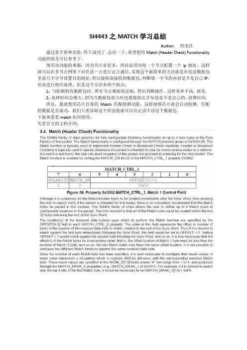
下面来看看match如何使用:先看官方的文档介绍:通过文档介绍,可以知道最多可以配置四字节在同步字之后的内容,分别用MACH_1—4L 来配置对应的MATCH_VALUE,MATCH_MASK,MATCH_CTRL,其中MATCH_VALUE里面填写要匹配的内容(比如我想将这个节点地址设为:0X01,因此本寄存器写入:0X01),MATCH_MASK 作为掩码可以来设置匹配检测哪几位(我这八位都检测,就设为:0XFF), MATCH_CTRL作为控制寄存器,第一个MATCH_CTRL_1中的第六位与其它3个控制寄存器不同,它作为使能控制,这里我们想使用MATCH就把它置1(该寄存器写入:0X40)。
上面的配置都是对MACH_1配置的,因为我只用一个字节的匹配,如果还想使用其他字节配置,自己再去配置2,3,4.看程序:Ok,把该段程序放到初始化程序里,然后就可以了,接下来在接收函数里写:SI446x_Status返回值是8个字节数据数组,每一个字节每一位对应的状态如下所示:我们可以看到SI446x_Status[2]这个字节里,即上表中的第三行,第八位表示这个匹配的判断结果,如果这位为1表明匹配成功,如果为0表明匹配失败。

si4463中文教程
简介
si4463是一款高性能、低功耗的无线收发器,常用于无线通信应用。
本教程将介绍如何使用si4463进行无线通信,包括硬件连接、驱动安装、配置和编程等内容。
硬件连接
在开始使用si4463之前,我们需要正确地连接硬件。
下面是si4463模块的引脚说明:
引脚名称描述
SDN上电复位控制引脚
GPIO通用输入/输出引脚
GND地
VCC电源(2.7V - 5.5V)
SCLK SPI时钟引脚
SDI SPI数据输入引脚
SDO SPI数据输出引脚
CS SPI片选引脚
将si4463模块的引脚与微控制器连接起来,并确保连接正确无误。
接下来,我们将介绍如何安装si4463的驱动。
驱动安装
为了能够成功地使用si4463模块,我们需要安装相应的驱动。
这里以Windows系统为例:
1.打开设备管理器,找到对应的串口设备,右键点击
并选择更新驱动程序。
2.选择手动更新驱动程序,然后选择从计算机中选择。
3.浏览到si4463驱动程序所在的文件夹,点击下一步。
4.完成驱动程序的安装。
完成驱动程序的安装后,我们还需要进行相应的配置和编程。
配置和编程
首先,在编程之前,我们需要下载并安装si4463的开发环境。
这里推荐使用Silicon Labs提供的开发工具。
1.在Silicon Labs官网下载并安装Si4463开发工具。
2.打开Si4463开发工具。
3.在工具中选择对应的芯片版本和项目设置。
4.单击。
.一.模块介绍 (2)1.1特点简介 (2)1.2电气参数 (3)1.3系列产品 (3)1.4常见问题 (3).二.功能简述 (4)2.1引脚定义 (4)2.2连接单片机 (5)2.3模块复位 (5)2.4AUX详解 (5).三.工作模式 (6)3.1模式切换 (7)3.2一般模式(模式0) (7)3.3唤醒模式(模式1) (7)3.4省电模式(模式2) (8)3.5休眠模式(模式3) (8)3.6快速通信测试 (8).四.指令格式 (9)4.1出厂默认参数 (9)4.2工作参数读取 (9)4.3版本号读取 (9)4.4复位指令 (9)4.5参数设置指令 (9).五.参数配置 (11).六.包装与焊接 (12).七.定制合作 (12).八.关于我们 (13).1.1E30-TTL-100是一款基于Silicon Labs公司原装进口SI4438射频芯片的无线串口模块(UART),半双工,收发一体,透明传输方式,发射功率100mW,工作在425~450.5MHz频段Array(默认433MHz),TTL电平输出,兼容3.3V与5V的IO口电压,具有空中唤醒功能(超低功耗)。
模块具有软件FEC前向纠错算法,其编码效率较高,纠错能力强,在突发干扰的情况下,能主动纠正被干扰的数据包,大大提高可靠性和传输距离。
在没有FEC的情况下,这种数据包只能被丢弃。
模块具有数据加密和压缩功能。
模块在空中传输的数据,具有随机性,通过严密的加解密算法,使得数据截获失去意义。
而数据压缩功能有概率减小传输时间,减小受干扰的概率,提高可靠性和传输效率。
1.21.3系列产品E30-TTL-1001.4常见问题E30-TTL-100.2.1*我司提供Altium designer封装库请前往下载或联系索取2.22.3模块复位E30-TTL-1002.4AUX详解E30-TTL-100AUX用于无线收发缓冲指示和自检指示。
它指示模块是否有数据尚未通过无线发射出去,或已经收到无线数据是否尚未通过串口全部发出,或模块正在初始化自检过程中。

apisix⾼性能⽹关-中⽂开发⽂档2020年6⽉12⽇13:48:33github:⽬前此项⽬已有成为apache孵化项⽬官⽅中⽂⽂档:⽀持的功能很多,我个⼈⽐较推荐服务发现,这个很省资源,不然得吧java的⼀套全部上上去,这样其他语⾔的也可以轻松做微服务了APISIXQQ 交流群: 552030619邮件列表: 发邮件到 dev-subscribe@, 然后跟着回复邮件操作即可。
APISIX 是⼀个云原⽣、⾼性能、可扩展的微服务 API ⽹关。
它是基于 Nginx 和 etcd 来实现,和传统 API ⽹关相⽐,APISIX 具备动态路由和插件热加载,特别适合微服务体系下的 API 管理。
为什么选择 APISIX?如果你正在构建⽹站、移动设备或 IoT(物联⽹)的应⽤,那么你可能需要使⽤ API ⽹关来处理接⼝流量。
APISIX 是基于云原⽣的微服务 API ⽹关,它是所有业务流量的⼊⼝,可以处理传统的南北向流量,也可以处理服务间的东西向流量,也可以当做 k8s ingress controller 来使⽤。
APISIX 通过插件机制,提供动态负载平衡、⾝份验证、限流限速等功能,并且⽀持你⾃⼰开发的插件。
功能你可以把 Apache APISIX 当做流量⼊⼝,来处理所有的业务数据,包括动态路由、动态上游、动态证书、A/B 测试、⾦丝雀发布(灰度发布)、蓝绿部署、限流限速、抵御恶意攻击、监控报警、服务可观测性、服务治理等。
全平台云原⽣: 平台⽆关,没有供应商锁定,⽆论裸机还是 Kubernetes,APISIX 都可以运⾏。
运⾏环境: OpenResty 和 Tengine 都⽀持。
⽀持 ARM64: 不⽤担⼼底层技术的锁定。
多协议: 动态 TCP/UDP 代理。
: ⽀持⽤client_id对 MQTT 进⾏负载均衡,同时⽀持 MQTT 和两个协议标准。
:通过 APISIX 代理 gRPC 连接,并使⽤ APISIX 的⼤部分特性管理你的 gRPC 服务。
APIsix的接口格式主要包含以下部分:
1. 请求方法(HTTP method):例如GET、POST、PUT、DELETE等。
2. 请求路径(URL path):表示请求的资源地址,具体由URL和查询参数构成。
3. 请求头(HTTP headers):用于传递一些附加信息,例如Content-Type、Authorization等。
4. 请求参数(query parameters):以键值对的形式附加在URL末尾,用于传递查询条件或参数。
5. 请求体(request body):包含POST或PUT请求中需要发送的数据,通常使用JSON格式。
6. 响应状态码(HTTP status code):表示API请求是否成功,常见的状态码有200、404、500等。
7. 响应头(HTTP headers):用于返回响应的附加信息,例如Content-Type、Server等。
8. 响应体(response body):包含API返回的实际数据,通常也是使用JSON格式。
以上是APIsix接口的基本格式,具体的接口定义可能因APIsix的具体实现和开发者的需求而有所不同。
在实际使用中,需要根据具体的API文档和开发指南来了解具体的接口格式和参数要求。
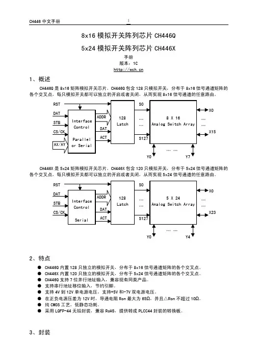
8x16模拟开关阵列芯片CH446Q5x24模拟开关阵列芯片CH446X手册版本:1C1、概述CH446Q是8x16矩阵模拟开关芯片。
CH446Q包含128只模拟开关,分布于8x16信号通道矩阵的各个交叉点,每只模拟开关都可以独立的开启或者关闭,从而实现8x16信号通道的任意路由。
CH446X是5x24矩阵模拟开关芯片。
CH446X包含120只模拟开关,分布于5x24信号通道矩阵的各个交叉点,每只模拟开关都可以独立的开启或者关闭,从而实现5x24信号通道的任意路由。
2、特点●CH446Q内置128只独立的模拟开关,分布于8x16信号通道矩阵的各个交叉点。
●CH446X内置120只独立的模拟开关,分布于5x24信号通道矩阵的各个交叉点。
●CH446Q支持7位并行地址输入,兼容现有同类产品。
●支持串行地址移位输入,节约引脚。
●支持4V到12V单电源电压,支持+5V和-7V双电源电压。
●在正负电源压差为12V时,导通电阻Ron最大为65Ω,并且△Ron不超过10Ω。
●纯CMOS工艺,低静态功耗。
●采用LQFP-44无铅封装,兼容RoHS,提供转成PLCC44封装的转换板。
3、封装封装形式宽度引脚间距封装说明订货型号LQFP-44 10*10mm 0.8mm 31.5mil 标准LQFP44脚贴片CH446Q LQFP-44 10*10mm 0.8mm 31.5mil 标准LQFP44脚贴片CH446X4、引脚4.1. CH446Q引脚引脚号引脚名称类型引脚说明38 VDD 电源正电源,电压必须大于等于GND12 GND 电源公共接地,数字信号参考地,电压为0V16 VEE 电源负电源,电压必须小于等于GND41 RST 输入外部手工复位输入,高电平有效10 P/-S 输入地址输入方式选择:高电平为并行输入方式;低电平为串行输入方式36 DAT 输入串行地址方式下,为串行数据输入和开关数据输入;并行地址方式下,为开关数据输入,为高电平时对应开启,为低电平时对应关闭14 STB 输入选通脉冲输入,高电平有效34 CS/CK 输入串行地址方式下,为串行时钟输入,上升沿有效;并行地址方式下,为片选输入,高电平有效43、18、19、42 AX0~AX3 输入串行地址方式下,为未用引脚,必须直接连接GND;并行地址方式下,为X端口选择的地址输入20、21、40 AY0~AY2 输入串行地址方式下,为未用引脚,必须直接连接GND;并行地址方式下,为Y端口选择的地址输入31、30、29、28、27、26、3、4、5、6、7、8、25、24、1、2 X0~X15模拟信号输入输出8x16矩阵模拟开关的X端口33、35、37、39、17、15、13、11 Y0~Y7模拟信号输入输出8x16矩阵模拟开关的Y端口9、22、23、32、44NC. 空脚未用引脚,禁止连接4.2. CH446X引脚引脚号引脚名称类型引脚说明38 VDD 电源正电源,电压必须大于等于GND12 GND 电源公共接地,数字信号参考地,电压为0V16 VEE 电源负电源,电压必须小于等于GND41 RST 输入外部手工复位输入,高电平有效36 DAT 输入串行数据输入和开关数据输入;作为开关数据输入时,高电平为开启,低电平为关闭14 STB 输入选通脉冲输入,高电平有效34 CS/CK 输入串行时钟输入,上升沿有效31、30、29、28、27、26、3、4、5、6、7、8、25、24、1、2、33、35、37、39、17、15、13、11 X0~X23模拟信号输入输出5x24矩阵模拟开关的X端口43、18、19、42、20 Y0~Y4模拟信号输入输出5x24矩阵模拟开关的Y端口9、10、21、40、22、23、32、44NC. 空脚未用引脚,禁止连接5、功能说明参考首页的框图,CH446Q芯片内部分为三个部分:接口控制逻辑、128只锁存器、128只模拟开关阵列。
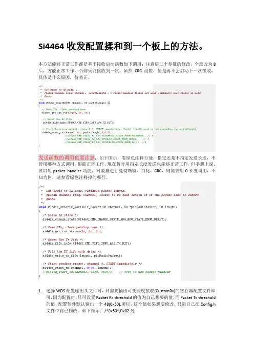
Si4464收发配置揉和到一个板上的方法。
本方法能够正常工作都是基于接收启动函数如下调用:注意后三个参数的修改,全部改为8后,方能正常工作,否则只能接收到一次。
虽然CRC没错,但是再不会启动下一次接收,具体是什么原因,待查正。
发送函数的调用也要注意:如下图示,看绿色注释行处,指定还是不指定发送长度,不管用哪种方式调用,都能正常工作。
现在暂时用指定长度发送也能够正常工作,但手册上说,要启用packet handler功能,对数据进行曼彻斯特、白化、CRC,则需要用0长度调用,不知为何,请参看绿色注释掉的哪行。
1.选择WDS配置输出头文件时,只需要输出可变长度接收(CustomRx)的寄存器配置文件即可,因为配置时,只可设置Packet Rx threshold的值为自己想要的值,而Packet Tx threshold 的值,配置软件默认输出一个48(0x30),所以,这个值如果想要修改,只能自己在Config.h 文件中自己修改。
如下图示:/*0x30*/0x02处2.在发送时再行修改Tx模式时寄存器的发送模式为单域,在config文件中切记要修改PKT_FIELD_2_CRC_CONFIG寄存器的配置:如下图中0x2A/*0x0A*/处。
3.发送函数前做如下配置:看最长的那行。
另外:注意黑条处的寄存器PKT_LEN,在发送时不用去管里头的长度大小端设置,其实,发送的时候就是配置寄存器的一个域工作就可了。
数据包的封装(与Rx端的协议)由用户自己在填充TxFIFO时,组织完成。
4.接收函数前做如下的配置:看最长的那行。
另外,注意,本配置中,未将长度字节配置填充到RxFIFO中。
若需要的话,可在下图选中Add length to RX FIFO即可:5.完整配置图如下:第一步:选中Custom packet RX,配置前导码,同步头,选2个域,设置接收缓冲阈值等,详见下图:第二步:选可变长度数据包模式,配置如下图示:第三步:配置同步头,这里选默认的2字节2D D4,同步头用户可自己1~4字节的任意值。
Si4463芯片使用小结一、芯片介绍Silicon Labs 的 Si4463芯片是高性能的低电流收发器,其覆盖了 119MHz 至 1050 MHz 的Sub-1GHz频段。
还是 EZRadioPRO系列的一部分,该系列包含覆盖各种应用的完整发射器、接收器和收发器产品线。
所有器件都具有杰出的灵敏度 -126 dBm,同时实现了极低的活动和休眠电流消耗。
二、功能实现1、引脚说明Si4463有20个引脚,主要引脚功能可以分为两大类:硬件引脚和软件引脚。
硬件引脚主要由电源、射频部分组成,软件引脚主要分为SPI、芯片使能以及GPIO。
硬件引脚在原理图、PCB设计部分需要注意,此处主要是介绍芯片的程序操作,硬件部分就此带过。
下表列举了si4463的21个引脚(包括芯片正下方的Exposed pad引脚)的具体引脚号和功能简述:表1 Si4463引脚简述Si446xPin Number Pin Name Pin Function Exposed pad, 18 GND Ground 6, 8 VDD Supply input2,3 Rxp,Rxn used for Rx4,7 Tx,TXRamp used for Tx16,17 Xin,Xout crystal11 NIRQ Interrupt output, active low1 SDN Shutdown input, active high15 NSEL SPI select input12 SCLK SPI clock input14 SDI SPI data input13 SDO SPI data output9 GPIO0 GPIO10 GPIO1 GPIO19 GPIO2 GPIO20 GPIO3 GPIO2、功能实现1)SPI操作芯片的12-15脚为SPI引脚,最大支持速率达到10MHz.芯片支持标准的SPI总线协议,操作方便。
整个芯片的所有SPI操作都可以分成两种方式:写命令和读数据。
SI4463 发送与接收不同步的问题si4463发送与接收不同步的问题Si4463发送和接收不同步si4463配置为使用变长度包传送模式,主机发送数据,从机接收数据,然后从机回传数据至主机。
发现在发送主机数据后,从机不会立即接收数据,而是经过一段延迟(延迟不是固定的,与数据包长度有关)。
在这里,将主设备和从设备的si4463上的nirq信号连接到示波器进行观察(在发送和接收启用数据包完成后中断)。
这里,通信前导字为8个字节,同步字为2个字节,包长度位为1个字节,包数据为8个字节,无crc。
数据串行速率为1kbps,主机理论上发送完毕需时间(8+2+1+8)*8/1k=0.152s,实际测试为160ms。
而示波器显示,从机经过0.12s后,nirq才变低。
从从机接收到rxfifo后,理论上rxfifo的数量应该是(1字节的数据包长度+8字节的数据=9),而从机nirq变低后,rxfifo的读取数量是0x18,即读取24,再读取15,理论时间是15*8/1K=0.12s,这与实际测量一致。
因为读取时是按包读取,即rxfifo第一个值为8(包长度),然后接下来只读取8个数据,并且在下次接收数据之前,会重新resetrxfifo,所以并不会出错(倘若在进行下次操作之前不重新resetrxfifo,则下次接收会出错)。
但仍然存在的问题是带来的延迟较大。
奇怪现象:如果从机只接收不发送,那么在主机发送后,从机也同时接收,rxfifo中的数字与主机发送的数字一致。
一旦执行发送操作,从机的接收将延迟,rxfifo的数量将异常。
因此,很自然地认为,如果在从机发送后再次初始化si4463(如通电初始化),下一次接收将与主机的传输同步。
事实也是如此。
然而,如果所有这些都重新初始化,也需要时间。
进一步发现,只有RF_pkt_len_uu12部分被初始化(由WDS自动生成的头文件)。
即在每次发送完毕后,重新配置下rf_pkt_len_12部分的寄存器(进一步发现是pkt_field_1_length_12_8、7_0),然后可保证从机下次接收与主机的发送同步。
Silicon Labs 无线收发器SI446x 的应用技巧Silicon Labs 的无线Sub-G 产品Si446x 现在已经越来越多的用于表计产品,如气表、电表等。
由于在表计类老产品中TI 的CC1101 系列应用非常广泛,所以客户使用Si446x 时,就会遇到和CC1101 兼容问题,本文档将解决此问题。
Si446x 具有硬件CRC、Whitening 和软件CRC、Whitening,因为不使用CRC、Whitening 和Manchester 时,Si446x 和CC1101 通信配置比较简单,可以参照Si446x works with CC1101_v1.11.pdf 文档,本文档只讨论CRC、Whitening 和Manchester 同时使能时配置方法。
Si446x 提供软件CRC、Whitening 算法支持和CC1101 兼容,需要将寄存器PKT_WHT_BIT_NUM 0x1205 的SW_WHT_CTRL 和SW_CRC_CTRL 位置1,使能SW whitening 和SW CRC。
为了确保Si446x 开启SW whitening 特性可以和CC1101 通信,寄存器PKT_WHT_SEED_15_8 0x1203 和PKT_WHT_SEED_7_0 0x1204 需要都设置为0xFF。
Si446x 最为发送端时,包格式需配置如下:由于已经开启SW CRC 和SW Whitening,所以必须关闭硬件CRC 和Whitening,以免重复计算CRC 和Whitening,寄存器PKT_FIELD_1_CONFIG 的PN_START 和WHITEN 位都清零,寄存器PKT_FIELD_1_CRC_CONFIG 也配置为0x00。
关闭了硬件CRC,为了发送由软件CRC 计算出的2 个字节CRC 的值,发送数据时需要多发送两个字节给TX FIFO 作为CRC 字节,并且配置Field1 的长度时,也需要额外增加2 个字节。
深圳市瑞诺信息技术有限公司RON1300产品说明书公司简介深圳市瑞诺信息技术有限公司是专业从事无线通讯产品开发、生产、销售、工程、与售后的综合企业,经过多年所有员工的不懈的努力取得了今日成绩,公司一直致力于高频无线智能产品及系统的研发、生产和销售。
无线产品的开发和ODM的项目维持了公司不断成长和壮大,公司在香港有专门的物流部门,深圳有专门的射频研发和生产,研发部备有完整的测试和调试仪器。
从频谱和信号源到网络分析仪全部具备,有专业的屏蔽室,有专业的静电测试仪器和高低温测试设备。
公司涉及领域:无线数传组网技术、无线射频识别技术 UHF(超高频)、RFID标签(tag)和读取器(reader)技术、智能家居系统,射频模拟前端和数字基带终端设计。
公司有专业射频研发高级工程师,从事多年无线产品开发。
有着多年的产品开发经验。
产品的稳定性和一致性是产品推广的基础,公司在产品的性能和功能上做了非常的大努力。
目录1.RON1300系列模组简介 (3)1.1.模组说明 (3)1.2.性能性能 (3)1.3.应用市场 (3)1.4.产品图片 (3)2.RON1300系列模组电器参数 (4)2.1.模组接线图及引脚描述 (4)2.2.模组电器参数 (4)3.RON1300系列模组使用说明 (6)3.1.RON1300模组软件编写和WDS使用说明 (7)4.RON1300系列模组参考软件 (9)5.RON1300模块原理图 (10)1.RON1300系列模组简介1.1模组接线图及引脚描述RON1300系列无线模组是专门用于远距离、小数据的无线数据传输系统。
它具有高数据传输速率和更远的传输距离。
该系列模组可以嵌入到现有产品或系统的设计当中,使通信可以更加容易、简洁。
客户只需在原有的微控制器件编译简单的通讯协议,即可激活双向通信实现数据传输。
RON1300系列模组RF部分是采用SILINCON LAB的Si4463设计,提供非常高的发射功率和接收灵敏度,可以让客户从现在有线系统在短时间内实现无线的转换。
Rev. 0.5 9/14Copyright © 2014 by Silicon LaboratoriesEZRadioPRO-DK1. Kits OverviewThis user's guide describes the development kits of the EZRadioPRO wireless development kit family. Each kit contains two RF nodes based on the Wireless Motherboard to support evaluation and development of sub-GHz RF links with the different EZRadioPRO devices. Table 1 lists the RF pico boards of the kits that use the latest C2A revision of the EZRadioPRO ICs. Table 2 lists the RF pico boards of the obsolete kits that use the previous B1B revision of the EZRadioPRO ICs. Table 3 lists the content that is common to all kits.Table 1. RF Pico Boards of the EZRadioPRO Development KitsQty DescriptionPart Number Si4461 Development Kit 868 MHz4461C-868-PDK 2Si4461 RF Transceiver Pico board 868 MHz, 14 dBm, direct tie 4461CPCE14D868-EK Si4438 Development Kit 490 MHz4438C-490-PDK 2Si4438 RF Transceiver Pico board 490 MHz, 20 dBm, direct tie 4438CPCE20D490-EK Si4463 Development Kit 915 MHz4463C-915-PDK 2Si4463 RF Transceiver Pico board 915 MHz, 20 dBm, switched4463CPCE20C915-EKTable 2. RF Pico Boards of the obsolete EZRadioPRO Development KitsQty DescriptionPart Number Si4060/Si4362 Development Kit 868MHz4060-868-PDK 1Si4060 RF Transmitter Pico Board 868MHz, 10dBm 4060-PCE10B868-EK 1Si4362 RF Receiver Pico Board 868MHz 4362-PRXB868-EK Si4063/Si4362 Development Kit 915MHz4063-915-PDK 1Si4063 RF Transmitter Pico board 915MHz, 20dBm 4063-PCE20B915-EK 1Si4362 RF Receiver Pico board 915MHz 4362-PRXB915-EK Si4461 Development Kit 868MHz4461-868-PDK 2Si4461 RF Transceiver Pico board 868MHz, 14dBm, direct tie 4461-PCE14D868-EKSi4438 Development Kit 490MHz4438-490-PDK 2Si4438 RF Transceiver Pico board 490MHz, 20dBm, direct tie 4438-PCE20D490Si4463 Development Kit 915MHz4463-915-PDK 2Si4463 RF Transceiver Pico Board 915MHz, 20dBm, switched4463-PCE20C915-EKTable 3. Content Common to Every KitQty DescriptionPart Number 2Wireless Motherboard MSC-WMB93X 2C8051F930 MCU Pico Board UPPI-930-RF2USB cable (USBA-USB mini)2Antenna with SMA connection MSC-AT50-XXX1Kit user guideEZRadioPRO-DK2. Software SetupThere are two software tools provided by Silicon Labs to aid in EZRadioPRO software development, the Wireless Development Suite (WDS) and the Silicon Labs Integrated Development Environment (IDE). The recommended starting point for EZRadioPRO development is the WDS software tool. This tool is able to identify the connected boards by reading their identification memories (EBID) and provides valuable help by greatly simplifying radio configuration, evaluation, and application development.2.1. Hardware and Software Requirements for WDSThe following hardware and software is required to run the WDS:⏹ Windows XP or later⏹ Microsoft .NET framework 3.5 or later⏹ Silicon Labs CP210x VCP driver⏹ WDS v3.2.7.0 or laterThe lack of the .NET framework and VCP driver are recognized during the WDS installation. The install wizard will install the missing components after prompting the user for consent.2.2. Download WDSWDS can be obtained from the Silicon Labs web site free of charge at/Support%20Documents/Software/WDS3-Setup.exe2.3. Installation StepsIf WDS is already installed on your machine, skip this section.Note:Before installing this software, local administration rights must be obtained from your network administrator.1. Start WDS3-Setup.exe.2. Click “Next” to start the installation process.3. Accept the license agreement by clicking the check box, and then press the “Next” button.4. Select the installation folder.It is recommended to use the default folder, C:\Program Files\Silabs\WDS35. When your settings are confirmed, click “Install” to continue.6. Click “Finish” to close the WDS Installer.EZRadioPRO-DK 3. Hardware SetupAfter checking the kit contents against Tables 2 and 3, the kit can be put into operation by performing the steps listed below.1. Insert an RF Pico board into the connectors labeled as CON1 and CON2 on the Wireless Motherboard(WMB).2. Insert a UPPI-930-RF MCU Pico Board into the connectors, J5, J6, J7, and J8, on the WMB. The dottedcorner of the F930 MCU has to point to the triangle symbol on the WMB.3. Connect the antenna to the SMA connector on the RF Pico Board.4. Set the SUPPLY SELECT switch to the USB position.5. Set the MCU DC/DC switch to the OFF position.6. Ensure that all the CURRENT MEASUREMENT jumpers are in place.7. Start the WDS on your PC.8. Using one of the USB cables in the kit, connect the WMB to the PC.9. If necessary wait for Windows to install the debug interface driver.10. WDS must identify the connected board and open an Application Manager window that lists informationabout the identified board.11. Boards are shipped without preloaded software. Sample codes can be configured and downloaded to theMCU from WDS. For details on how to use the WDS, see the WDS User's Guides listed in "4. UsefulDocumentation" on page 5".EZRadioPRO-DKFigure 2.WDS Application Manager WindowRepeat steps 1 to 9 for the other node of the kit.The two nodes are now ready for evaluation. Detailed descriptions of the example codes can be found in the programming guide listed in "4. Useful Documentation" on page 5.The following is a quick-step guide to performing simple packet TX/RX.1. Leave both nodes powered from the USB as described above.2. Select “Radio Configuration Application”.3. From the Radio Configuration Application window, select “Standard Packet TX” for one node and “StandardPacket RX” for the other node.4. 4Leave the default parameter settings untouched; simply click “Download project”.5. Now, the simple TX/RX sample project is running on the boards. When pressing one of the SW1 to SW4buttons on the TX board, packets are sent, and the corresponding LED of LED1 to LED4 lights up during the transmission. On the RX side, LED1 is always on, while different combinations of LED2 to LED4 light up during successful packet reception according to the button pressed.EZRadioPRO-DK 4. Useful DocumentationFor general information on the EZRadioPRO chips, see the following data sheets:⏹ Si406x Data Sheet⏹ Si4362 Data Sheet⏹ Si446x Data SheetFor hardware design guidance, see the following application notes:⏹ AN627: Si4060/Si4460/61 Low-Power PA Matching⏹ AN629: Si4460/61/63/64 RF ICs Layout Design Guide⏹ AN643: Si446x/Si4362 RX LNA Matching⏹ AN648: Si4063/Si4463/64 TX MatchingFor detailed information on lab measurements and data sheet parameter verification, refer to the following application notes:⏹ AN655: Range Test Application for EZRadio® and EZRadioPRO®⏹ AN796: Wireless Development Suite General Description⏹ AN632: WDS User's Guide for EZRadioPRO® DevicesFor detailed information on programming the radio, refer to the following documents:⏹ Si406x API Descriptions⏹ Si4362 API Descriptions⏹ Si446x API Descriptions⏹ AN633: Programming Guide for EZRadioPRO® Si4x6x Devices⏹ Download WDS3 installer⏹ Download Silicon Laboratories IDE installerMore useful documents can be accessed via the EZRadioPRO web pages at/products/wireless/EZRadioPRO/Pages/default.aspxEZRadioPRO-DK5. The Wireless Motherboard Hardware PlatformThe wireless motherboard platform is a demo, evaluation, and development platform for EZRadioPRO radio ICs. It consists of a wireless motherboard and interchangeable MCU and RF pico boards.Figure 3.8-bit Wireless Motherboard PlatformEZRadioPRO-DK5.1. The Wireless MotherboardFigure 4.Wireless MotherboardThe wireless motherboard contains four pushbuttons, four LEDs, and a buzzer as simple user interfaces. A graphical LCD displays menu items for range testing purposes and a potentiometer demonstrates analog capabilities of the MCU. A switch supports the power options of the MCU's built-in dc/dc converter. Using the current measurement jumpers, current consumption can be measured separately either for the MCU, the radio, or the peripherals. The motherboard contains test pins for all I/O pins of the MCU and for all digital pins of the radio. In addition, there are SMA connectors for the GPIOs of the radio for test equipment connection. A USB communication interface as well as a built-in Silicon Labs USB-to-C2 debug adapter are integrated onto the board so that the wireless motherboard (WMB) can be directly connected via USB to the PC for downloading and debugging code on the MCU.An interface connection towards sensor modules can also be found. The MCU is also connected to the RF pico board through a connector pair.MCU Pico BoardRF Pico BoardCurrentMeasurement PinsRadio Test PinsRadio GPIO ConnectorsBuzzerReset Button Push Buttons Potentiometer MCU DC/DC Converter Switch MCU Test PinsPower Supply Switch Sensor Module Connector External Power Supply Connection USBCommunication and Debug InterfaceEZRadioPRO-DK5.2. Power SchemeThe power source of the platform can be selected with the power supply selector switch “SUPPLY SELECT” on the WMB board. If this switch is in the ”USB” position, supply voltage is provided by the PC that is connected to the ”J16” mini USB connector. If this switch is in the ”BAT” position, the supply voltage is provided by two AA batteries in the battery holder on the bottom side of the board. If the ”SUPPLY SELECT” switch is in the ”EXT” position, supply voltage is provided by an external power source through the ”TP7” and “TP9” points.Using the ”MCU dc/dc” switch, the internal dc/dc converter of the C88051F930 MCU on the MCU pico board can be activated if the connected pico board supports this function. If the switch is in ”OFF” position, the MCU's dc/dc converter is inactive and the supply voltage is only determined by the state of the “SUPPLY SELECT” switch. Positioning the switch to either ”LDO (1.25V)” or ”1 CELL” position will turn on the MCU's dc/dc converter by connecting 1.25–1.5V supply voltage to the VBAT pin and removing external power from the VDC pin. The MCU will provide 1.9V in default setting on its VDC pin to all the other connected loads. Since this current is limited, it may be necessary to disconnect or disable some loading part of the board. For further details, see the MCU data sheet and the board schematic. The board schematic can be found in the EZRadioPRO Development Kit User's Guide. A complete CAD design pack of the board is also available at .5.3. RF Pico BoardFigure5.RF Pico Board Front SideThe RF pico board is a radio module that contains an EZRadioPRO radio IC, matching network and an SMA connector on the top side. These components apart from the antenna connector are covered by a metal shield for noise reduction. The digital signals of the radio (SCLK, SDI, SDO, NSEL, SCL, SDA, VDD and GND) can be accessed on test points at the edge of the board. The boards also have a factory loaded board identification memory (EBID) on the bottom side that contains data that describes the board properties. Via the unified RF pico connector pair on the bottom side of the board, any RF pico board can be connected to the WMB.EZRadioPRO-DKThe schematic of an RF Pico Board can be found in the next chapter. The complete CAD design pack of each RF pico board type is also available at .5.4. Setting up and Connecting the WMB to the PCSteps for connecting the platform to the PC:1. Connect an RF Pico Board to the WMB board through the CON1 and CON2 connectors.2. Insert a UPPI-930-RF MCU pico board in the connectors J5, J6, J7, J8 on the WMB. The dotted corner of the C8051F930 MCU has to point to the triangle symbol on the WMB.3. Connect an antenna to the SMA connector on the RF Pico Board.4. Select the desired power source with the SUPPLY SELECT switch.5. Ensure that all the CURRENT MEASUREMENT jumpers are in place.6. Connect the WMB board to a USB port of the PC.7. Wait for Windows to install the driver of the debug interface if necessary.Table 4. Connections between the WMB Board and the RF Pico BoardSi446x, Si4362, Si406x, Si4438WMBC8051F930Pin NumberPin Name Pin Function RF Pico board J1connectorWMB Con2 connector Pin Name EP ,18GND Ground 21,2,19,20GND 8VDD Voltage Supply input 117,18VDD 11NIRQ Interrupt output active low 107P0.11SDN Shutdown input active high 38P2.315NSEL SPI select input 66P1.412SCLK SPI clock input 95P1.014SDI SPI data input 73P1.213SDO SPI data output 84P1.19GPIO_0General Purpose I/O 1211P2.6 (2nd)10GPIO_1General Purpose I/O 1112P1.319GPIO_2General Purpose I/O 513P2.520GPIO_3General Purpose I/O414P2.4EZRadioPRO-DK6. Wireless Motherboard SchematicsF i g u r e 6.W i r e l e s s M o t h e r b o a r d S c h e m a t i c (1 o f 4)F i g u r e 7.W i r e l e s s M o t h e r b o a r d S c h e m a t i c (2 o f 4)F i g u r e 8.W i r e l e s s M o t h e r b o a r d S c h e m a t i c (3 o f 4)F i g u r e 9.W i r e l e s s M o t h e r b o a r d S c h e m a t i c (4 o f 4)F i g u r e 10.R F P i c o B o a r dF i g u r e 11.U P P I -930-R F M C U P i c o B o a r d S c h e m a t i c (1 o f 2)F i g u r e 12.U P P I -930-R F M C U P i c o B o a r d S c h e m a t i c (2 o f 2)C ONTACT I NFORMATIONSilicon Laboratories Inc.400 West Cesar ChavezAustin, TX 78701Tel: 1+(512) 416-8500Fax: 1+(512) 416-9669Toll Free: 1+(877) 444-3032Please visit the Silicon Labs Technical Support web page:https:///support/pages/contacttechnicalsupport.aspxand register to submit a technical support request.Patent NoticeSilicon Labs invests in research and development to help our customers differentiate in the market with innovative low-power, small size, analog-intensive mixed-signal solutions. Silicon Labs' extensive patent portfolio is a testament to our unique approach and world-class engineering team.The information in this document is believed to be accurate in all respects at the time of publication but is subject to change without notice.Silicon Laboratories assumes no responsibility for errors and omissions, and disclaims responsibility for any consequences resulting from the use of information included herein. Additionally, Silicon Laboratories assumes no responsibility for the functioning of undescribed fea-tures or parameters. Silicon Laboratories reserves the right to make changes without further notice. Silicon Laboratories makes no warran-ty, representation or guarantee regarding the suitability of its products for any particular purpose, nor does Silicon Laboratories assume any liability arising out of the application or use of any product or circuit, and specifically disclaims any and all liability, including without limitation consequential or incidental damages. Silicon Laboratories products are not designed, intended, or authorized for use in applications intend-ed to support or sustain life, or for any other application in which the failure of the Silicon Laboratories product could create a situation where personal injury or death may occur. Should Buyer purchase or use Silicon Laboratories products for any such unintended or unauthorized application, Buyer shall indemnify and hold Silicon Laboratories harmless against all claims and damages.Silicon Laboratories and Silicon Labs are trademarks of Silicon Laboratories Inc.Other products or brandnames mentioned herein are trademarks or registered trademarks of their respective holders.。