APR3001-45A中文资料
- 格式:pdf
- 大小:153.22 KB
- 文档页数:15
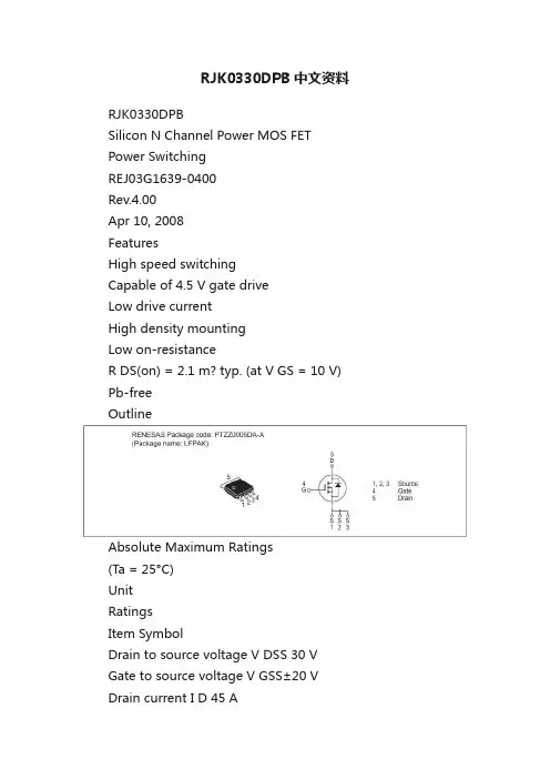
RJK0330DPB中文资料RJK0330DPBSilicon N Channel Power MOS FET Power SwitchingREJ03G1639-0400Rev.4.00Apr 10, 2008FeaturesHigh speed switchingCapable of 4.5 V gate driveLow drive currentHigh density mountingLow on-resistanceR DS(on) = 2.1 m? typ. (at V GS = 10 V) Pb-freeOutlineAbsolute Maximum Ratings(Ta = 25°C)UnitRatingsItem SymbolDrain to source voltage V DSS 30 V Gate to source voltage V GSS±20 V Drain current I D 45 ADrain peak current I D(pulse)Note1 180 ABody-drain diode reverse drain current I DR 45 A Avalanche current I AP Note 2 22 A Avalanche energy E AR Note 2 48.4 mJ Channel dissipation Pch Note3 55 WChannel to Case Thermal Resistance θch-C 2.27 °C/WCha nnel temperature Tch 150 °CStorage temperature Tstg –55 to +150 °CNotes: 1. PW ≤ 10 μs, duty cycle ≤ 1%2. Value at Tch = 25°C, Rg ≥ 50 ?3. Tc = 25°CElectrical Characteristics(Ta = 25°C)Item Symbol Min Typ Max Unit Test ConditionsDrain to source breakdownvoltageV (BR)DSS 30 —— V I D = 10 mA, V GS = 0 Gate to source leak current I GSS ——±0.1 μA V GS = ±20 V, V DS = 0 Zero gate voltage drain current I DSS ——1 μA V DS = 30 V, V GS = 0 Gate to source cutoff voltage V GS(off) 1.2 — 2.5 V V DS = 10 V, I D = 1 mAR DS(on) — 2.1 2.7 m ? I D = 22.5 A, V GS = 10 V Note4 Static drain to source on stateresistance R DS(on) — 2.8 3.9 m ? I D = 22.5 A, V GS = 4.5 V Note4 Forward transfer admittance |y fs | — 90 — S I D = 22.5 A, V DS = 10 V Note4 Input capacitance Ciss — 4300 — pF Output capacitance Coss — 800 — pFReverse transfer capacitance Crss — 245 — pF V DS = 10 V, V GS = 0,f = 1 MHz Gate Resistance Rg — 0.4 — ? Total gate charge Qg — 27 — nC Gate to sourcecharge Qgs — 10.5 — nCGate to drain charge Qgd — 5.8 — nC V DD = 10 V, V GS =4.5 V,I D = 45 A Turn-on delay time t d(on) — 6.8 — ns Rise time t r — 3.9 — nsTurn-off delay time t d(off) — 50 — ns Fall timet f — 5.4 — ns V GS = 10 V, I D = 22.5 A,V DD ? 10 V, R L = 0.44 ?, Rg = 4.7 ? Body–drain diode forward voltage V DF — 0.78 1.02 V I F = 45 A, V GS = 0 Note4 Body–drain diode reverse recovery timet rr — 36 — ns I F = 45 A, V GS = 0di F / dt = 100 A/ μs Body–drain diode reverse recovery charge Q rr — 34 — nCNotes: 4. Pulse testMain CharacteristicsPackage DimensionsOrdering InformationPart No. Quantity Shipping Containerpcs TapingRJK0330DPB-00-J0 2500Refer to "/en/network " for the latest and detailed information.Renesas Technology America, Inc.450 Holger Way, San Jose, CA 95134-1368, U.S.A Tel: <1> (408) 382-7500, Fax: <1> (408) 382-7501Renesas Technology Europe LimitedDukes Meadow, Millboard Road, Bourne End, Buckinghamshire, SL8 5FH, U.K.Tel: <44> (1628) 585-100, Fax: <44> (1628) 585-900Renesas Technology (Shanghai) Co., Ltd.Unit 204, 205, AZIACenter, No.1233 Lujiazui Ring Rd, Pudong District, Shanghai, China 200120Tel: <86> (21) 5877-1818, Fax: <86> (21) 6887-7858/7898Renesas Technology Hong Kong Ltd.7th Floor, North Tower, World Finance Centre, Harbour City, Canton Road, Tsimshatsui, Kowloon, Hong Kong Tel: <852> 2265-6688, Fax: <852> 2377-3473Renesas Technology Taiwan Co., Ltd.10th Floor, No.99, Fushing North Road, Taipei, Taiwan Tel: <886> (2) 2715-2888, Fax: <886> (2) 3518-3399Renesas Technology Singapore Pte. Ltd.1 Harbour Front Avenue, #06-10, Keppel Bay Tower, Singapore 098632 Tel: <65> 6213-0200, Fax: <65> 6278-8001Renesas Technology Korea Co., Ltd.Kukje Center Bldg. 18th Fl., 191, 2-ka, Hangang-ro, Yongsan-ku, Seoul 140-702, Korea Tel: <82> (2) 796-3115, Fax: <82> (2) 796-2145Renesas Technology Malaysia Sdn. BhdUnit 906, Block B, Menara Amcorp, Amcorp Trade Centre, No.18, Jln Persiaran Barat, 46050 Petaling Jaya, Selangor Darul Ehsan, Malaysia Tel: <603> 7955-9390, Fax: <603> 7955-9510 RENESAS SALES OFFICES。
ACCESSORIESLMSHELF = Mounting Shelf 300-450W MXSHELF = Mounting Shelf 72-200W C1063R49/02 IHOrdering InformationSERIES DC WATTAGE HEADS HEADS OPTIONS 1CCL = 6 Volt 6 Volt6 Volt3 = Three A = Ammeter 2TCL = 12 Volt75 = 75 Watts DY = 8 Watt, Tungsten 2 = Two ACF1 = 120 VAC Fuse 100 = 100 Watts DA = 18 Watt, Tungsten 1 = OneACF2 = 277 VAC Fuse 150 = 150 Watts DL = 25 Watt, Tungsten ACP1 = 120 VAC Power Switch 225 = 225 WattsDC = 30 Watt, Tungsten ACP2 = 277 VAC Power Switch AD = ACCU-TEST Self-Diagnostics 12 Volt (Includes standard voltmeter)12 VoltADAL = ACCU-TEST with Alarm150 = 150 Watt DNY = 12 Watt, Tungsten ADTD = ACCU-TEST with Time Delay 3200 = 200 Watt DE = 28 Watt, Tungsten DCP = DC Power Switch300 = 300 Watt DK = 25 Watt, Tungsten EX = Special Input Transformer (Specify voltage and frequency)450 = 450 WattDG = 30 Watt, TungstenTD1 = 120 VAC Time Delay 3TTD2 = 277 VAC Time Delay 3(Suggested lamp heads listedV = Voltmeter 2above. Refer to the Accessories Section for W = White Housingadditional lamp head choices.)CCL15016.0”(40.6 cm)TCL300, TCL4506.0”(15.2 cm)7.6”(19.3 cm)12.0”(30.5 cm)27.0”(12.7 cm)6.0”(15.2 cm)7.6”(19.3 cm)12.0”(30.5 cm)Notes:1) Some option combinations may impact UL list-ing. consult factory for specifics.2) Not available witj AD, ADAL, or ADTD options.3) 15 minute delay.元器件交易网Housing18 gauge steel housing with a tan epoxy powder coat finish.Knockouts provided for mounting up to three lamp heads.The suggested lamp head is the “D” Series round sealed beam Par 36 tungsten. To order lamp heads other than the suggested “D” head, refer to Chloride Accessories Section..Suggested SpecificationFurnish and install Chloride Systems emergency lighting unit model ________. The unit shall be constructed to meet Underwriter’s Laboratories, Inc. Standard #924and the National Electrical Code (NEC).INSTALLATION AND OPERATION -Unit shall be easily field connected to a 120 or 277 VAC, 60 hertz, unswitched power source. Installation must comply with the NEC as well as other applicable codes. Upon utility power failure or brownout, the unit shall automatically transfer to battery power and maintain the required illumina-tion level for a minimum period of 90 minutes. Upon restoration of utility power, the charger shall restore the battery to full charge within UL 924 requirements follow-ing a rated discharge of not more than 90 minutes.CHARGER -Product shall utilize a fully automatic, voltage regulated, two-rate current limited solid-state charger. The charging system shall maintain the battery at full capacity without the need for periodic exercising or equalization. The following features shall be standard: Low voltage disconnect (LVD), brownout protection and AC lockout.BATTERY -The battery shall be a low maintenance, free electrolyte, wet cell, lead calcium battery. The lead calcium battery shall provide trouble-free operation in temperatures up to 85°F (30°C).HOUSING -The unit housing shall be constructed of 18 gauge steel with a tan epoxy powder coat finish.Chloride SystemsISO 9001A2528C1063R49/02 IH272 West Stag Park Service Road •Burgaw NC 28425Telephone: (910) 259 1000 •Facsimile: (800) 258 Lamp Head Photometrics(For DL, suggested head for CCL)(For DK, suggested head for TCL)Vertical203050100Up 2010feet 010Down 20.2.1406070.31.5Horizontal203050100Left 2010feet 010Right 20.2.1406070.31.5203050100Up 2010feet 010Down 20Photometric No. 3406070801.3.2.1.5Horizontal203050100Left 3010feet 01020Right 301.3.2.120.540607080。
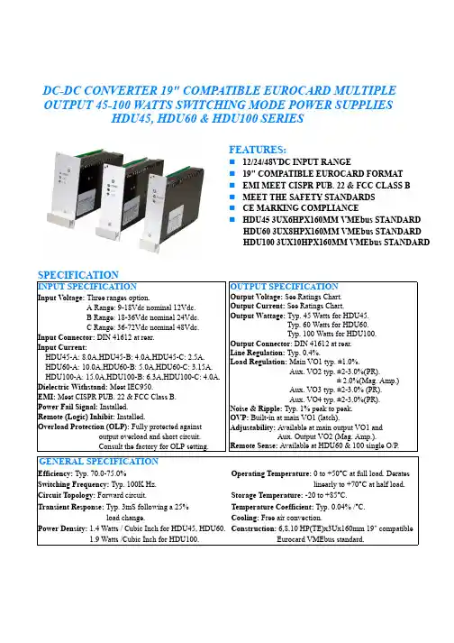
DC-DC CONVERTER 19" COMPATIBLE EUROCARD MULTIPLE OUTPUT 45-100 WATTS SWITCHING MODE POWER SUPPLIES HDU45, HDU60 & HDU100 SERIESFEATURES:12/24/48VDC INPUT RANGE19" COMPATIBLE EUROCARD FORMATEMI MEET CISPR PUB. 22 & FCC CLASS BMEET THE SAFETY STANDARDSCE MARKING COMPLIANCEHDU45 3UX6HPX160MM VMEbus STANDARDHDU60 3UX8HPX160MM VMEbus STANDARDHDU100 3UX10HPX160MM VMEbus STANDARD SPECIFICATIONINPUT SPECIFICATIONInput Voltage: Three ranges option.A Range: 9-18Vdc nominal 12Vdc.B Range: 18-36Vdc nominal 24Vdc.C Range: 36-72Vdc nominal 48Vdc.Input Connector: DIN 41612 at rear.Input Current:HDU45-A: 8.0A,HDU45-B: 4.0A,HDU45-C: 2.5A.HDU60-A: 10.0A,HDU60-B: 5.0A,HDU60-C: 3.15A.HDU100-A: 15.0A,HDU100-B: 6.3A,HDU100-C: 4.0A.Dielectric Withstand: Meet IEC950.EMI: Meet CISPR PUB. 22 & FCC Class B.Power Fail Signal: Installed.Remote (Logic) Inhibit: Installed.Overload Protection (OLP): Fully protected againstoutput overload and short circuit.Consult the factory for OLP setting.OUTPUT SPECIFICATIONOutput Voltage: See Ratings Chart.Output Current: See Ratings Chart.Output Wattage: Typ. 45 Watts for HDU45.Typ. 60 Watts for HDU60.Typ. 100 Watts for HDU100.Output Connector: DIN 41612 at rear.Line Regulation: Typ. 0.4%.Load Regulation: Main VO1 typ. ±1.0%.Aux. VO2 typ. ±2-3.0%(PR).± 2.0%(Mag. Amp.)Aux. VO3 typ. ±2-3.0% (PR).Aux. VO4 typ. ±2-3.0%(PR).Noise & Ripple: Typ. 1% peak to peak.OVP: Built-in at main VO1 (latch).Adjustability: Available at main output VO1 andAux. Output VO2 (Mag. Amp.).Remote Sense: Available at HDU60 & 100 single O/P. GENERAL SPECIFICATIONEfficiency: Typ. 70.0-75.0%Switching Frequency: Typ. 100K Hz.Circuit Topology: Forward circuit.Transient Response: Typ. 3mS following a 25%load change.Power Density: 1.4 Watts / Cubic Inch for HDU45, HDU60.1.9 Watts /Cubic Inch for HDU100.Operating Temperature: 0 to +50°C at full load. Derateslinearly to +70°C at half load.Storage Temperature: -20 to +85°C.Temperature Coefficient: Typ. 0.04% /°C.Cooling: Free air convection.Construction: 6,8,10 HP(TE)x3Ux160mm 19" compatibleEurocard VMEbus standard.OUTPUT VOLTAGE/CURRENT RATINGS CHARTHDU45 SeriesMECHANICAL DIMENSIONS: MM [INCHES] WEIGHT: HDU45 537.0g (18.94 Oz.)SINGLE OUTPUTINPUT RANGEOUTPUT VO1 @◇ MODEL NO.Vdc Typ. Volt.HDU45-A or B or C-S033 A: 9-18,B: 18-36,C: 36-72 10.0A 3.3V HDU45-A or B or C-10 A: 9-18,B: 18-36,C: 36-72 9.0A 5.0V HDU45-A or B or C-11 A: 9-18,B: 18-36,C: 36-72 4.0A 12.0V HDU45-A or B or C-12 A: 9-18,B: 18-36,C: 36-72 3.0A 15.0V HDU45-A or B or C-13A: 9-18,B: 18-36,C: 36-72 2.0A 24.0VDUAL OUTPUTINPUT RANGEOUTPUT VO1 @◇ OUTPUT VO2 ●◇■ MODEL NO.Vdc Typ. Volt. Typ. Volt.HDU45-A or B or C-D033E A: 9-18,B: 18-36,C: 36-72 5.0A 3.3V 4.0A 5.0V HDU45-A or B or C-D033I A: 9-18,B: 18-36,C: 36-72 5.0A 3.3V 2.0A 12.0V HDU45-A or B or C-20 A: 9-18,B: 18-36,C: 36-72 4.0A 5.0V 2.0A 12.0V HDU45-A or B or C-21 A: 9-18,B: 18-36,C: 36-72 2.0A 12.0V 2.0A 12.0V HDU45-A or B or C-23 A: 9-18,B: 18-36,C: 36-72 1.5A 15.0V 1.5A 15.0V HDU45-A or B or C-24 A: 9-18,B: 18-36,C: 36-72 4.0A 5.0V 1.0A 24.0V HDU45-A or B or C-25 A: 9-18,B: 18-36,C: 36-72 1.0A 24.0V 1.0A 24.0VTRIPLE OUTPUTINPUT RANGEOUTPUT VO1 @◇ OUTPUT VO2 ●◇■ OUTPUT VO3 ●◇■ MDEL NO.Vdc Typ. Volt. Typ. Volt. Typ. Volt. HDU45-A or B or C-T033EI A: 9-18,B: 18-36,C: 36-72 5.0A 3.3V 4.0A 5.0V 0.50A 12.0V HDU45-A or B or C-T033IM A: 9-18,B: 18-36,C: 36-72 5.0A 3.3V 2.0A 12.0V 0.25A 24.0VHDU45-A or B or C-30 A: 9-18,B: 18-36,C: 36-72 3.0A 5.0V 2.0A 12.0V 0.50A 5.0V HDU45-A or B or C-31 A: 9-18,B: 18-36,C: 36-72 3.0A 5.0V 2.0A 15.0V 0.50A 15.0V HDU45-A or B or C-32 A: 9-18,B: 18-36,C: 36-72 3.0A 5.0V 2.0A 12.0V 0.50A 12.0V HDU45-A or B or C-33 A: 9-18,B: 18-36,C: 36-72 3.0A 5.0V 1.0A 24.0V 0.50A 12.0VSymbol: " "OVP built-in. "@"Adjustable. "●" Installed with Post Regulator. "■" Couple filter inductor. "◇" Floating ( or isolated) output.INPUT & OUTPUT CONNECTORS PIN ASSIGNMENTSDC INPUTSINGLE/DUAL/TRIPLE OUTPUTASSORTED SIGNAL ASSIGNMENT +Vin -Vin G +VO1 -VO1 +VO2 -VO2 +VO3 -VO3 NC LOG. INH. +S -SPOWERFAILHDU45-1X28 30 32 4,6 12,14 - - - - 16,18,24,26 20 8 10 22 HDU45-2X28 30 32 4 6 8 10 - - 12,14,16,18,24,26 20 - - 22 HDU45-3X28 30 32 4,6, 8,10 12 14 16 18 24,26 20 - - 22HDU60 SeriesSINGLE OUTPUTINPUT RANGEOUTPUT VO1 @#◇ MODEL NO.Vdc Typ. Volt.HDU60-A or B or C-S033 A: 9-18,B: 18-36,C: 36-72 16.0A 3.3V HDU60-A or B or C-10 A: 9-18,B: 18-36,C: 36-72 12.0A 5.0V HDU60-A or B or C-11 A: 9-18,B: 18-36,C: 36-72 5.0A 12.0V HDU60-A or B or C-12 A: 9-18,B: 18-36,C: 36-72 4.0A 15.0V HDU60-A or B or C-13A: 9-18,B: 18-36,C: 36-72 2.5A 24.0VDUAL OUTPUTINPUT RANGEOUTPUT VO1 @◇ OUTPUT VO2▲◇@ MODEL NO.Vdc Typ. Volt. Typ. Volt.HDU60-A or B or C-D033E A: 9-18,B: 18-36,C: 36-72 6.0A 3.3V 5.0A 5.0V HDU60-A or B or C-D033I A: 9-18,B: 18-36,C: 36-72 6.0A 3.3V 3.0A 12.0V HDU60-A or B or C-20 A: 9-18,B: 18-36,C: 36-72 5.0A 5.0V 3.0A 12.0V HDU60-A or B or C-21 A: 9-18,B: 18-36,C: 36-72 2.5A 12.0V 2.5A 12.0V HDU60-A or B or C-23 A: 9-18,B: 18-36,C: 36-72 2.0A 15.0V 2.0A 15.0V HDU60-A or B or C-24 A: 9-18,B: 18-36,C: 36-72 5.0A 5.0V 1.5A 24.0V HDU60-A or B or C-25A: 9-18,B: 18-36,C: 36-72 1.3A 24.0V 1.3A 24.0VTRIPLE OUTPUTINPUT RANGEOUTPUT VO1 @◇ OUTPUT VO2 ▲◇@ OUTPUT VO3 ●◇■ MDEL NO.Vdc Typ. Volt. Typ. Volt. Typ. Volt. HDU60-A or B or C-T033EI A: 9-18,B: 18-36,C: 36-72 6.0A 3.3V 5.0A 5.0V 0.50A 12.0V HDU60-A or B or C-T033IM A: 9-18,B: 18-36,C: 36-72 6.0A 3.3V 2.5A 12.0V 0.25A 24.0VHDU60-A or B or C-30 A: 9-18,B: 18-36,C: 36-72 5.0A 5.0V 2.5A 12.0V 1.00A 5.0V HDU60-A or B or C-31 A: 9-18,B: 18-36,C: 36-72 4.5A 5.0V 2.0A 15.0V 0.50A 15.0V HDU60-A or B or C-32 A: 9-18,B: 18-36,C: 36-72 5.0A 5.0V 2.5A 12.0V 0.50A 12.0V HDU60-A or B or C-33 A: 9-18,B: 18-36,C: 36-72 5.0A 5.0V 1.3A 24.0V 0.50A 12.0V"#" Remote sensing. "◇" Floating ( or isolated) output.INPUT & OUTPUT CONNECTORS PIN ASSIGNMENTSDC INPUTSINGLE/DUAL/TRIPLE OUTPUTASSORTED SIGNALASSIGNMENT +Vin -Vin G +VO1 -VO1 +VO2 -VO2 +VO3 -VO3 NC LOG. INH. +S -SPOWERFAILHDU60-1X28 30 32 4,6 12,14 - - - - 16,18,24,26 20 8 10 22 HDU60-2X28 30 32 4 6 8 10 - - 12,14,16,18,24,26 20 - - 22 HDU60-3X28 30 32 4,6, 8,10 12 14 16 18 24,26 20 - - 22HDU100 SeriesMECHANICAL DIMENSIONS: MM [INCHES] WEIGHT: HDU100 943.0g (33.26 Oz.)SINGLE OUTPUTINPUT RANGEOUTPUT VO1 @#◇ MODEL NO.Vdc Typ. Volt.HDU100-A or B or C-S033 A: 9-18,B: 18-36,C: 36-72 25.0A 3.3V HDU100-A or B or C-10 A: 9-18,B: 18-36,C: 36-72 20.0A 5.0V HDU100-A or B or C-11 A: 9-18,B: 18-36,C: 36-72 8.5A 12.0V HDU100-A or B or C-12 A: 9-18,B: 18-36,C: 36-72 7.0A 15.0V HDU100-A or B or C-13A: 9-18,B: 18-36,C: 36-72 4.5A 24.0VDUAL OUTPUTINPUT RANGEOUTPUT VO1 @◇ OUTPUT VO2▲◇ MODEL NO.Vdc Typ. Volt. Typ. Volt.HDU100-A or B or C-D033E A: 9-18,B: 18-36,C: 36-72 10.0A 3.3V 8.0A 5.0V HDU100-A or B or C-D033I A: 9-18,B: 18-36,C: 36-72 10.0A 3.3V 5.0A 12.0VHDU100-A or B or C-20 A: 9-18,B: 18-36,C: 36-72 8.0A 5.0V 5.0A 12.0V HDU100-A or B or C-21 A: 9-18,B: 18-36,C: 36-72 4.2A 12.0V 4.2A 12.0V HDU100-A or B or C-23 A: 9-18,B: 18-36,C: 36-72 3.4A 15.0V 3.4A 15.0V HDU100-A or B or C-24 A: 9-18,B: 18-36,C: 36-72 8.0A 5.0V 2.5A 24.0V HDU100-A or B or C-25 A: 9-18,B: 18-36,C: 36-72 2.1A 24.0V 2.1A 24.0VTRIPLE OUTPUTINPUT RANGEOUTPUT VO1 @◇ OUTPUT VO2 ▲◇@ OUTPUT VO3 ●◇■ MDEL NO.Vdc Typ. Volt. Typ. Volt. Typ. Volt. HDU100-A or B or C-T033EI A: 9-18,B: 18-36,C: 36-72 6.0A 3.3V 5.0A 5.0V 0.50A 12.0V HDU100-A or B or C-T033IM A: 9-18,B: 18-36,C: 36-72 6.0A 3.3V 2.5A 12.0V 0.25A 24.0VHDU100-A or B or C-30 A: 9-18,B: 18-36,C: 36-72 7.0A 5.0V 5.0A 12.0V 1.00A 5.0V HDU100-A or B or C-31 A: 9-18,B: 18-36,C: 36-72 6.0A 5.0V 4.0A 15.0V 0.60A 15.0V HDU100-A or B or C-32 A: 9-18,B: 18-36,C: 36-72 7.0A 5.0V 5.0A 12.0V 0.50A 12.0V HDU100-A or B or C-33 A: 9-18,B: 18-36,C: 36-72 7.0A 5.0V 2.5A 24.0V 0.50A 12.0V"#" Remote sensing. "◇" Floating ( or isolated) output.INPUT & OUTPUT CONNECTORS PIN ASSIGNMENTSDC INPUT SINGLE/DUAL/TRIPLE OUTPUTASSORTED SIGNAL ASSIGNMENT +Vin -Vin G +VO1 -VO1 +VO2 -VO2 +VO3 -VO3 NC LOG. INH. +S -SPOWERFAILHDU100-1X28 30 32 4,6 12,14 - - - - 16,18,24,26 20 8 10 22 HDU100-2X28 30 32 4 6 8 10 - - 12,14,16,18,24,26 20 - - 22 HDU100-3X28 30 32 4,6, 8,10 12 14 16 18 24,26 20 - - 22 Mating connector: DIN41612-H15 Female。
Derating CurveAQF-30 is a 30-Watt series of AC-DC power modules. These modules have universal input range of 85-265VAC and are available in 13 models with efficiency as high as 80%.Other features include continuous short circuit protection,overvoltage protection, output current limitation, EMCEN61000-4(-2,-3,-4) and EMI EN55022 level B approved which conducted noise compliance minimize design-in time, cost and eliminate the need for external components.The AQF-30 series has IEC / EN / UL 60950-1 safety approval qualifies this product for worldwide markets. The series is a wide variety of applications including in commercial and industrial of theMTBF 250,000 hours.yOperating Temperature 71] (Reference to Derating Curve)yIEC61140 Safety Class II ApprovalyUL 60950-1 Safety Approval y MTBF > 250,000 Hours y EMC Complies With EN61000y EMI Complies With EN55022 Class B and FCC part 15, level B y I/O Isolation 3000VACy PCB and Chassis Mounting Packages y Single, Dual and Triple Output Modules y 85~265VAC, 47~440Hz Universal Input Range y High Efficiency up to 80%Key FeaturesSingle, Dual and Triple Outputs30 Watts Universal Input Range AC/DC Power Modules150050050250+12220020003001500+57160483220053008004000*3.3AQF-30T3512P150050050250+12220015002201000+3.37160588220060009004500*5AQF-30T5312P1500750-50-500-15150075050500157660572220045003003000*5AQF-30T5151500500-50-250-12150015002001000127660572220045006003000*5AQF-30T512A1500900-120-600-121500900120600127660572220045006003000*5AQF-30T512150018001251250*127660572390045003003000*5AQF-30D5128060543# 1500---{100{1000{15AQF-30D158060565# 1500---{130{1300{12AQF-30D1280605431000---6362548AQF-30S4880605431500---125125024AQF-30S2480605433900---200200015AQF-30S1580605433900---250250012AQF-30S1278605578000---60060005AQF-30S05% (Typ.)mA (Typ.)mA (Typ.)uF mA mA mA VDC @Max. Load@No Load @Max. Load Max.Peak Min.Max.115VAC, 60Hz Efficiency Input CurrentCapacitive LoadOutput CurrentOutput VoltageModel NumberModel Selection Guide*Output floating (see note 8)# For each outputB C C30% 10ms 60% 100ms 95% 5000msEN61000-4-11B0.15~80MHz 10Vrms (functional earth portsincluded)80% AM 1kHz modulationEN61000-4-6B1.2/50uS(8/20uS)AC dif. {1KV DC {0.5KV EN61000-4-5BAC port {2KV DC, SL, TL {2KV not less than 1 min.EN61000-4-4A80~1000MHz 10V/m 80% AM1KHz modulation EN61000-4-3BAir {8KV Cont. {4KV EN61000-4-2Performance Criteriaspecification requirement Standard Conducted EMCEN55022 Class BConducted EMIFree-Air Convection Cooling %95---Humidity ]85-40Storage Temperature ]71-25AmbientOperating Temperature 1. Specifications typical at Ta=+25], resistive load, 115VAC, 60Hz input voltage, rated output current unless otherwise noted.2. Ripple & Noise measurement bandwidth is 0~20 MHz.3. These power modules require a minimum output loading to maintain specified regulation.4. Operation under no-load conditions will not damage these devices; however they may not meet all listed specifications.5. Other input and output voltage may be available, please contact factory.6. Specifications subject to change without notice.7. Peak current can’t be drawn from all output at the same time.8. Floating (or isolated) output of a power supply that is not connected to any other output.9. To order the power module with chassis mounting style, please add a suffix C (e.g.AQF-30S05C). 10. Part Number for DIN-Rail bracket:AC-DIN-02Unit Max.Min.Conditions ParameterNote:Environmental SpecificationsA40------230VACA 20------115VAC Inrush Current (Cold Start at 25])Hz 440---47Input Frequency RangeVAC 265---85All Models Input Voltage Range Unit Max.Typ.Min.Conditions ParameterInput SpecificationsHiccup mode, indefinite (automatic recovery)Short Circuit Protection%------10585VAC, Hiccup technique, auto-recoveryCurrent Limitation %5------Overshoot %/]---{0.02---Temperature Coefficient % of Vo ---120---Zener diode clampOver Voltage Protection %V pp of Vo 1.31.0---Other Output Models %V pp of Vo 1.81.5---3.3 & 5.0VDC Output ModelsRipple & Noise (20MHz)%---{5.0---Vo3%---{5.0---Vo2%---{2.0---Measured output Io = 20% to 100% of rated loadOther output are set at 50% of rated loadVo1Cross Regulation- Dual Positives / Triple Output %---{4.0---Vo2&Vo3%{5.0{2.5---Vo1Triple Output Models%{5.0{2.5---Dual Output Models %{1.0{0.5---Single Output ModelsIout=Min. to Max.Load Regulation%{1.0{0.2---Vin=Min. to Max.Line Regulation%---{3.0---Vo2&Vo3%{2.0{1.0---Vo1Dual Positive / Triple Output%{2.0{1.0---Single / Dual OutputOutput Voltage Accuracy Unit Max.Typ.Min.Conditions ParameterOutput SpecificationsK Hours------250MIL-HDBK-217F @ 25], Ground BenignMTBFms ---20---115VAC, 60HzHold-up Time KHz ---100---Switching Frequency M[------100500VDCIsolation Resistance VDC ------4700Input to Output, Flash Tested for 1 SecondIsolation Test Voltage VAC ------3000Input to Output, 60 SecondsIsolation Voltage Unit Max.Typ.Min.ConditionsParameterGeneral Specifications1.5A Slow - Blow TypeExternal Fuse (Recommended)3.5A / 250VAC Built-in FuseAll ModelsInput FuseTriple Output 2Triple Output 1Dual Output 2Dual Output 1Single OutputBlock DiagramUL94V-0:Flammability191g :Weight Plastic resin + Fiberglass :Case Material 4.41*2.51*1.01 inches 112.0*63.8*25.6 mm :Case SizePhysical CharacteristicsNC: No Connection+Vout3-Vout3NC-Vout NC7-Vout1-Vout1-Vout1NC6Common 2/3Common 2/3-Vout2Common -Vout 5+Vout1+Vout1+Vout1NC 4+Vout2+Vout2+Vout2+Vout+Vout3AC(L) - AC Line 2AC(N) - AC Neutral1Triple Output2Triple Output1Dual Output2Dual Output1Single OutputPin Pin ConnectionsChassis mountingUL94V-0:Flammability177g :Weight Plastic resin + Fiberglass :Case Material 3.50*2.50*0.85 inches 88.9*63.5*21.5 mm :Case Size Physical CharacteristicsNC: No Connection+Vout3-Vout3NC-VoutNC7-Vout1-Vout1-Vout1No Pin6Common 2/3Common 2/3-Vout2Common -Vout 5+Vout1+Vout1+Vout1No Pin 4+Vout2+Vout2+Vout2+Vout +Vout 3AC(L) - AC Line2AC(N) - AC Neutral1Triple Output2Triple Output1Dual Output2Dual Output1Single OutputPin PCB mountingPin ConnectionsMechanical Dimensions{0.004{0.1Pin X.XXX{0.01X.XX{0.25X.XX{0.02X.X{0.5Inches Millimeters Tolerance UL94V-0:FlammabilityPin ConnectionsDIN-Rail Package。
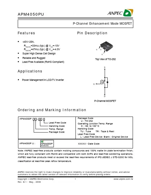
ANPEC reserves the right to make changes to improve reliability or manufacturability without notice, and advise customers to obtain the latest version of relevant information to verify before placing orders.APM4050PHandling Code Temp. Range Package CodePackage Code U : TO-252Operating Junction Temp. Range C : -55 to 150 C Handling CodeTU : Tube TR : Tape & Reel Lead Free CodeL : Lead Free Device Blank : Original Device APM4050P U :APM4050P XXXXXXXXXX - Date CodeLead Free Code Pin DescriptionOrdering and Marking InformationFeaturesApplications• -40V/-25A,R DS(ON)=33m Ω (typ.) @ V GS =-10V R DS(ON)=47m Ω (typ.) @ V GS =-4.5V• Super High Dense Cell Design • Reliable and Rugged• Lead Free Available (RoHS Compliant)• Power Management in LCD/TV InverterTop View of TO-252P-Channel MOSFETGDSGNote: ANPEC lead-free products contain molding compounds and 100% matte tin plate termination finish;which are fully compliant with RoHS and compatible with both SnPb and lead-free soldiering operations.ANPEC lead-free products meet or exceed the lead-free requirements of IPC/JEDEC J STD-020C for MSL classification at lead-free peak reflow temperature.°Absolute Maximum RatingsElectrical Characteristics (T= 25°C unless otherwise noted)AN otes:a : Pulse test ; pulse width≤300ms, duty cycle≤2%.b : Guaranteed by design, not subject to production testing.Typical CharacteristicsPower Dissipation P t o t - P o w e r (W )T j - Junction Temperature (°C)-I D - D r a i n C u r r e n t (A )Drain CurrentT j - Junction Temperature (°C)Safe Operation Area-V DS - Drain - Source Voltage (V)-I D - D r a i n C u r r e n t (A )N o r m a l i z e d T r a n s i e n t T h e r m a l R e s i s t a n c eThermal Transient ImpedanceSquare Wave Pulse Duration (sec)1E-41E-30.010.11101000.010.11220406080100120140160180102030405060204060801001201401600510152025300.1110100-I D - D r a i n C u r r e n t (A )R D S (O N ) - O n - R e s i s t a n c e (m Ω)Drain-Source On Resistance-I D - Drain Current (A)-V GS - Gate - Source Voltage (V)T j - Junction Temperature (°C)Gate Threshold VoltageN o r m a l i z e d T h r e s h o l d V l o t a g eTypical Characteristics (Cont.)-50-2502550751001251500.00.20.40.60.81.01.21.4R D S (O N ) - O n - R e s i s t a n c e (m Ω)024681012141618201020304050607080123456789102030405060708090100Drain-Source On ResistanceN o r m a l i z e d O n R e s i s t a n c eT j - Junction Temperature (°C) -V SD - Source - Drain Voltage (V)-I S - S o u r c e C u r r e n t (A )-V DS - Drain - Source Voltage (V)C - C a p a c i t a n c e (p F )CapacitanceGate ChargeQ G - Gate Charge (nC)-V G S - G a t e -s o u r c e V o l t a g e (V )Typical Characteristics (Cont.)0.111020510152025300300600900120015000.00.20.40.60.81.01.21.41.61.82.0246810Package InformationTO-252 (Reference JEDEC Registration TO-252)Physical SpecificationsT LT P25T e m p e r a t u r eTimeReflow Condition (IR/Convection or VPR Reflow)Classification Reflow ProfilesCarrier Tape & Reel DimensionsReliability Test ProgramClassification Reflow Profiles(Cont.)Carrier Tape & Reel Dimensions (Cont.)Cover Tape DimensionsCustomer ServiceAnpec Electronics Corp.Head Office :No.6, Dusing 1st Road, SBIP,Hsin-Chu, Taiwan, R.O.C.Tel : 886-3-5642000Fax : 886-3-5642050Taipei Branch :7F, No. 137, Lane 235, Pac Chiao Rd.,Hsin Tien City, Taipei Hsien, Taiwan, R. O. C.Tel : 886-2-89191368Fax : 886-2-89191369。
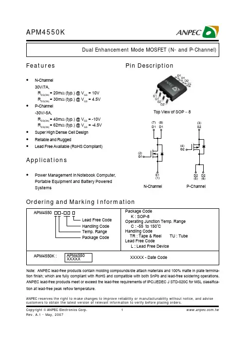
Copyright © ANPEC Electronics 1ANPEC reserves the right to make changes to improve reliability or manufacturability without notice, and advise customers to obtain the latest version of relevant information to verify before placing orders.APM4550KFeaturesApplicationsPin DescriptionOrdering and Marking InformationTop View of SOP − 8Note: ANPEC lead-free products contain molding compounds/die attach materials and 100% matte in plate termina-tion finish; which are fully compliant with RoHS and compatible with both SnPb and lead-free soldering operations.ANPEC lead-free products meet or exceed the lead-free requirements of IPC/JEDEC J STD-020C for MSL classifica-tion at lead-free peak reflow temperature.N-Channel P-Channel•N-Channel 30V/7A,R DS(ON) = 20m Ω (typ.) @ V GS = 10V R DS(ON) = 30m Ω (typ.) @ V GS = 4.5V•P-Channel -30V/-5A,R DS(ON) = 40m Ω (typ.) @ V GS = -10V R DS(ON) = 62m Ω (typ.) @ V GS = -4.5V•Super High Dense Cell Design •Reliable and Rugged•Lead Free Available (RoHS Compliant)•Power Management in Notebook Computer,Portable Equipment and Battery Powered SystemsG2(4)(3)(5)(6)G1(8)(7)(2)(1)APM4550Handling Code Temp. Range Package CodePackage Code K : SOP-8Operating Junction Temp. RangeC : -55 to 150 CHandling CodeTR : Tape & Reel TU : Tube Lead Free CodeL : Lead Free Device APM4550K :APM4550XXXXXXXXXX - Date CodeLead Free Code °Absolute Maximum Ratings (TA= 25°C unless otherwise noted)Electrical Characteristics (TA = 25°C unless otherwise noted)Copyright © ANPEC Electronics 2Copyright © ANPEC Electronics 3Notes:a : Pulse test ; pulse width ≤300µs, duty cycle ≤ 2%.b : Guaranteed by design, not subject to production testing.Electrical Characteristics (Cont.) (T A = 25°C unless otherwise noted)Copyright © ANPEC Electronics 4Typical CharacteristicsI D - D r a i n C u r r e n t (A )Drain CurrentT j - Junction Temperature (°C)Safe Operation AreaV DS - Drain - Source Voltage (V)Thermal Transient ImpedanceSquare Wave Pulse Duration (sec)Power DissipationP t o t - P o w e r (W )T j - Junction Temperature (°C)I D - D r a i n C u r r e n t (A )N-ChannelN o r m a l i z e d T r a n s i en t T h e r m a l R e s i s t a n c e 0204060801001201401600.00.51.01.52.02.5123456781E-41E-30.010.1110301E-30.010.1120.010.11101000.010.1110100Copyright © ANPEC Electronics Corp.5T j - Junction Temperature (°C)V GS - Gate - Source Voltage (V)-50-250255075100125150Copyright © ANPEC Electronics 6V DS - Drain - Source Voltage (V)Drain-Source On Resistance N o r m a l i z e dO n R e s i s t a n c e T j - Junction Temperature (°C)C - C a p a c i t a n c e (p F )V SD - Source - Drain Voltage (V)Source-Drain Diode ForwardI S - S o u r c e C u r r e n t (A )Capacitance Gate ChargeQ G - Gate Charge (nC)V G S - G a t e - s o u r c e V o l t a g e (V )Typical Characteristics (Cont.)N-Channel-50-252550751001251500.000.250.500.751.001.251.501.752.000.11103010020030040050060070080090010002468101214012345678910Copyright © ANPEC Electronics 7Typical Characteristics (Cont.)Power DissipationP t o t - P o w e r (W )T j - Junction Temperature (°C)-I D - D r a i n C u r r e n t (A )Drain Current T j - Junction Temperature (°C)Safe Operation Area-V DS - Drain - Source Voltage (V)Thermal Transient ImpedanceSquare Wave Pulse Duration (sec)-I D - D r a i n C u r r e n t (A )P-ChannelN o r m a l i z e d T r a n s i en t T h e r m a l R e s i s t a n c e 0204060801001201401600.00.51.01.52.02.51234560.010.11101000.010.1110501E-41E-30.010.1110301E-30.010.112Copyright © ANPEC Electronics 8T j - Junction Temperature (°C)-V GS - Gate - Source Voltage (V)2345678910Copyright © ANPEC Electronics 9Typical Characteristics (Cont.)Drain-Source On ResistanceN o r m a l i z e d O n R e s i s t a n c eT j - Junction Temperature (°C)-V SD - Source - Drain Voltage (V)Source-Drain Diode Forward -I S - S o u r c e C u r r e n t (A )-V DS - Drain - Source Voltage (V)C - C a p a c i t a n c e (p F )CapacitanceGate ChargeQ G - Gate Charge (nC)-V G S - G a t e - s o u r c e V o l t a g e (V )P-Channel0.00.20.40.60.8 1.0 1.2 1.4 1.60.11102010020030040050060070080024681012012345678910-50-252550751001251500.20.40.60.81.01.21.41.61.82.0Copyright © ANPEC Electronics 10Package InformationSOP-8S Y M B O LMIN.MAX.1.750.100.170.250.25A A1c D E E1e h L MILLIMETERS b 0.310.513.90 BSC SOP-80.250.500.40 1.270.154 BSC MIN.MAX.INCHES0.0690.0040.0120.0200.0070.0100.0100.0200.0160.05000.0104.90 BSC 0.193 BSC 6.00 BSC 0.236 BSC 1.00 BSC0.050 BSCA2 1.250.0490°8°0°8°VIEW A SEATING PLANEGAUGE PLANE °Carrier Tape & Reel Dimensions(mm) Devices Per ReelCopyright © ANPEC Electronics 11Copyright © ANPEC Electronics 12T LT P25T e m p e r a t u r eTimeReflow Condition (IR/Convection or VPR Reflow)Classification Reflow ProfilesPhysical SpecificationsNotes: All temperatures refer to topside of the package. Measured on the body surface.Copyright © ANPEC Electronics 13Customer ServiceAnpec Electronics Corp.Head Office :No.6, Dusing 1st Road, SBIP,Hsin-Chu, Taiwan, R.O.C.Tel : 886-3-5642000Fax : 886-3-5642050Taipei Branch :7F, No. 137, Lane 235, Pao Chiao Rd.,Hsin Tien City, Taipei Hsien, Taiwan, R. O. C.Tel : 886-2-89191368Fax : 886-2-89191369Reliability Test ProgramTable 1. SnPb Eutectic Process – Package Peak Reflow TemperaturesTable 2. Pb-free Process – Package Classification Reflow TemperaturesClassification Reflow Profiles (Cont.)。
MPA300LSeriesInputParameterConditionsMin.Typ.Max.Units Input Voltage Range Universal90264VAC Input Frequency4763Hz Input Current, Full Load 90 - 264 VAC 8A Inrush Current, Cold Start 110 VAC 17.5A 220 VAC 35Leakage Current (Note 1)240 VAC 1.5mAPower Factor Correction Active, Meets EN61000-3-2 Class DInput ProtectionT8A/250V FuseOutputParameterConditionsMin.Typ.Max.Units Output Voltage Adjustment By Trim Pot ±5.0%Output Regulation (Note 2)±1.0%Hold Time80% Load 20mSec Ripple & Noise (20 MHz) (Note 3)See Model Selection Guide Overload Protection Hiccup Mode 110140%Over Voltage Protection>130% of Rated Output Voltage. Recycle AC Input.Over Temperature Protection >+85ºC Ambient with AutorecoveryTemperature Coeffi cient±0.04%/ºC Transient Recovery Time (Note 4)50% Load Change2.5mS Transient Response Deviation 5%Overshoot/Undershoot At Turn On/Off 5.0%Turn On Delay120 VAC 1SOutput Short CircuitContinuous With Autorecovery GeneralParameter ConditionsMin.Typ.Max.Units Isolation Voltage Input - Output3,000VACInput - FG (Frame Ground)1,500Primary - Core1,500Switching FrequencyFixed23kHzInterface SignalsPower Supply OnBi-Color LED on the PCB, Green for power ON, Orange whenprotection is enabled or the the unit is inhibited (see remote 0n/0ff)Power Good Signal PG on CN3. Goes TTL high 100 to 500 mS after regulation. Goes low atleast 1 mS before the loss of regulation. Will sink 100 mA.Remote Sense V1S + and V1S- on CN3. Compensates for up to a 0.5V line drop. (noton models with current share option)Remote On/OffINH on CN3. A TTL low signal inhibits the outputEnvironmentalParameterConditionsMin.Typ.Max.UnitsOperating Temperature Range Ambient 0+25+50ºC Output Derating2.5%/ ºC from +50 ºC to + 70 ºCStorage Temperature Range -20+85ºCCoolingSee Model Selection GuideOperating Humidity RH, Non-condensing 90%Vibration, 5 ~ 50 HzAcceleration of ±7.35 m/(S x S) on X, Y and Z axisReliability Specifi cationsParameter Conditions Min.Typ.Max.UnitsMTBFMIL HDBK 217F , 30ºC, Gnd Benign 100kHours Safety Standards UL 60950; CSA C22.2 No. 60950; TUV EN60950; CB Report (IEC 60950)EMI ComplianceCompliance to EN55022 (CISPR22) Class B; EN61000-3-2,3EMS Immunity ComplianceEN6100-4-2,3,4,5,6,8,11; EN55024,; CE Marked (L VD)Electrical Specifi cationsSpecifi cations typical @ +25°C, nominal input voltage & rated output current, unless otherwise noted. Specifi cations subject to change without notice.to change without notice.i h iNEW Industrial Power!!Key Features:• 300W Output Power• Universal 90-264V AC Input • PFC to EN61000-3-2 “D”• UL, cUL, TUV Approvals • CE Certifi ed• FCC Class B Emissions • 12V to 55V Outputs• Remote Sense /Remote On/Off • Three Mechanical OptionsLow Profi le 300W Single OutputPower Factor CorrectedAC/DC Power SuppliesMicroPower Direct292 Page Street Suite DStoughton, MA 02072USAT: (781) 344-8226F: (781) 344-8481E: sales@ W:Model Selection GuideMechanical Dimensions: U-Chassis (U Suffi x)MicroPower Direct292 Page Street Ste D Stoughton, MA 02072 • TEL: (781) 344-8226 • FAX: (781) 344-8481 •E-Mail: sales@Model Number Output Voltage Output Current (Notes 6, 7, 8)Ripple &Noise Effi ciency(Note 7)Factory PreSet Range (Note 5)(“U” units) Max.with 22 CFM Min“E” UnitsInt. Fan MPA300Lx-12zz 12 VDC 12.0 - 15.0 VDC 25.00A 0.0A 25.00A 1% p-p 80%MPA300Lx-18zz 18 VDC 16.0 - 21.0 VDC 18.75A 0.0A 18.75A 1% p-p 80%MPA300Lx-24zz 24 VDC 22.0 - 30.0 VDC 13.64A 0.0A 13.64A 1% p-p 80%MPA300Lx-36zz 36 VDC 31.0 - 41.0 VDC 9.68A 0.0A 9.68A 1% p-p 80%MPA300Lx-48zz48 VDC 42.0 - 55.0 VDC 7.15A 0.0A 7.15A1% p-p80%Notes:1. Models are available with leakage current specifi ed as low as 750 µA. Contact the factory for details.2.Output regulation includes line & load.3.Ripple & noise is measured from 10 Hz to 20 MHz. Measurement connection to the unit is made with a 0.1 µF ceramic capacitor & a 22 µF electrolytic capacitor con-nected in parallel.4. Transient recovery is measured to within a 1% error bandfor a load step change of 50% to 100%.5. The full output range (see table above) is covered in the safety agency certifi cation. Stan-dard models are factory set to the “Preset” voltage. This may be set to other levels within the range without affecting the agency certifi cation. Contact the factory for details.6. A minimum 1% load is required to maintain load regulation and ripple specifi cations.7. Output current is given for the factory preset voltage. For more information, contact the factory.8. Units will provide peak power of 900W for 500 µS. For units capable of longer durations,contact the factory.U-Chassis Cover (C Suffi x)Enclosure With Fan (E Suffi x)Input Connector CN1:U-Chassis (U,A)Howder Terminal Block No. HI-201-39 (3-pin), 9.5 mm center or Mating Molex Part No. 09-91-0500 (5 pin, 3 used) or equivalent.Enclosed with Fan (E)Dinkle Terminal Block No. DT-35-A02W-3 (3-pin).Output Connector CN2:Howder Terminal Block No. HD-121-6P (6-pin) orMating Molex Part No. 09-91-2000 (14 pin) or equivalent. Output Pin Assignment:Howder Molex Pins 1 ~ 3: V+ Pins 1 ~ 7: V+ Pins 4 ~ 6: V-Pins 8 ~ 14: V-Logic Signal Connector CN3:Mating JST XHP-5 or equivalent (CHYAO SHI-UNN JS-2001-05).Fan driver connector (FAN):12 VDC / 400 mA is available to drive an external fan. Mating JST XHP-2 or equivalent (CHYAOSHIUNN JS-2001-02).。
AC/DC Power SupplyFEATURES• 2 Year Warranty• 100% Full Load Burn-In Test• Universal AC Input/ Full Range• Low Leakage Current < 0.75mA• Cooling by Free Air Convection• Fixed Switching Frequency at 65KHz• Short Circuit, Overload, and Over Voltage ProtectedSPECIFICATIONS:PSPT45 SeriesAll specifications are based on 25o C, Nominal Input Voltage, and Maximum Output Current unless otherwise noted.We reserve the right to change specifications based on technological advances.INPUT SPECIFICATIONSInput Voltage 90 – 264VAC (127 – 370VDC)Input Frequency 47 ~ 440HzAC Current (typical) 1A @ 115VAC 0.7A @ 230VACInrush Current 15A @ 115VAC cold start 30A @ 230VAC cold start.Leakage Current < 0.75mAOUTPUT SPECIFICATIONSOutput Voltage See TableOutput Voltage Tolerance (See Note 3) CH 1: ±4% CH.2: ±7% CH 3: ±5%Voltage Adjustment Range CH1: 4.75 ~ 5.5VOutput Power (max) Rated output power for convection; 52W with 18CFM min. forced air.Line Regulation CH 1: ±1% CH.2: ±2% CH 3: ±1%Load Regulation CH 1: ±3% CH.2: ±4% CH 3: ±1%Output Current See TableRipple & Noise (See Note 2) See tableSetup, Rise Time 800ms, 20ms at full loadHold Up Time 60ms at full loadTemperature Coefficient ±0.04%/°C (0~50°C) on +5V output.PROTECTIONOver Voltage Protection CH.1: 5.75 ~ 6.75VDCProtection Type: Hiccup mode, recovers automatically after fault condition is removed.Overload Protection 53 ~ 75W rated output power.Protection Type: Hiccup mode, recovers automatically after fault condition is removed.GENERAL SPECIFICATIONSSwitching Frequency (fixed) 65KHzEfficiency (typical) 75%Withstand Voltage 3KVAC (input to output), 1.5KVAC (input to FG), 0.5KVAC (output to FG). All for one minute. Isolation Resistance 100MΩ / 500VDC (input to output, input to FG, output to FG)ENVIRONMENTAL SPECIFICATIONSWorkingTemperature -10°C to +60°C (refer to output load derating curve)Storage Temperature -20°C to +85°CWorking Humidity (non-condensing) 20% ~ 90% RH non-condensingStorage Humidity (non-condensing) 10% ~ 95% RHVibration 10~500Hz, 2G 10min./1cycle, Period for 60 minutes each along X, Y, and Z axes.MTBF 288,100 hours min. MIL-HDBK-217 (25°C)PHYSICAL SPECIFICATIONSWeight 28 oz.Dimensions 127(L) x 76(W) x 28(H) mmWarranty 2 yearsSAFETY & EMCSafety Standards UL60950-1, TUV EN60950-1 ApprovedEMI Conduction and Radiation Compliance to EN55022 (CISPR22) Class BHarmonic Current Compliance to EN61000-3-2,3EMS Immunity Compliance to EN61000-4-2,3,4,5,6,8,11; ENV50204, EN55024, Light industry level, criteria A.AC/DC Power SupplyOUTPUT VOLTAGE / CURRENT RATING CHARTModelInput VoltageOutput VoltageOutput Current RangeRatedOutput CurrentRipple &Noise Output Power Channel 1 5 VDC 0.4 ~ 5A 3A 50mVp-p Channel 2 12 VDC 0.2 ~ 2.5A 2A 120mVp-p PSPT-45AChannel 3 -5 VDC 0 ~ 0.5A 0.3A 50mVp-p 40.5WChannel 1 5 VDC 0.4 ~ 5A 3A 50mVp-p Channel 2 12 VDC 0.2 ~ 2.5A 2A 120mVp-p PSPT-45BChannel 3 -12 VDC 0 ~ 0.5A 0.3A 100mVp-p 42.6WChannel 1 5 VDC 0.4 ~ 5A 3A 50mVp-p Channel 2 15 VDC 0.2 ~ 2.3A 1.6A 120mVp-p PSPT-45C Channel 390~264 VAC(127~370 VDC)-15 VDC0 ~ 0.5A0.3A100mVp-p43.5WNOTES1. All parameters not specially mentioned are measured at 230VAC input, rated load, and 25°C ambient temperature.2. Ripple & noise are measured at 20MHz using a 12" twisted pair-wire terminated with 0.1uF & 47uF capacitors in parallel .3. Tolerance: includes set up tolerance, line regulation, and load regulation.4. The power supply is considered a component, which will be installed into final equipment. The final equipment must be re- confirmed that it still meets EMC directives.5. Mounting holes M1 and M2 should be grounded for EMI purposes.BLOCK DIAGRAMDERATING CURVE STATIC CHARACTERISTICS (B)fosc: 65KHzAC/DC Power Supply MECHANICAL DRAWINGUnit: mmAC INPUT CONNECTOR (CN1)Pin. No Assignment1 AC/N2 AC/LDC OUTPUT CONNECTOR (CN2)Pin No. Assignment1 +V 2,3 +5V 4,5 COM6 -V。
PMW3000电动机保护控制器使用说明书博耳(宜兴)电力成套有限公司Boer (Yixing) Power System Co., Ltd目录第一章概述 01.1 概述 01.2 产品特点 0第二章技术指标 (2)2.1 环境要求指标 (2)2.2 技术参数 (2)2.3 精度指标 (2)2.4 接口参数 (3)2.5 绝缘电阻及介质强度 (3)2.6 机械性能 (4)2.7 抗电磁干扰(EMC)性能 (4)2.8 安装方式 (4)第三章产品结构 (5)3.1 硬件结构 (5)3.2 主控单元 (6)第四章产品功能 (9)4.1 装置功能表 (9)4.2 测量功能 (10)4.3 模拟量输出功能 (11)4.4 开关量输入 (12)4.5 开关量输出 (12)4.6 通讯接口 (12)4.7 辅助保护功能 (13)4.8 开关量控制功能 (19)4.9 装置告警 (19)4.10 事件记录功能 (19)4.11 PT、CT变比设置 (20)第五章人机界面操作说明 (21)5.1 装置面板布置图 (21)5.2 键盘说明 (21)5.3 信号灯指示说明 (22)5.4 显示菜单说明 (23)第六章用户调试细则 (34)6.1 通电前检查项目 (34)6.2 通电检查项目 (34)6.3 模拟保护试验 (35)第七章定值一览表 (36)附录A PMW3001原理接线图 (40)附录B PMW3001端子接线图 (41)附录C PMW3001外形尺寸 (42)附录D PMW3001实物图 (45)1.1 概述PMW3001电动机保护控制器是一种数字式智能型电动机保护控制设备,直接针对一台低压电动机设计,能够完成一台低压电动机的测量、控制及辅助保护功能,具有很高的性能价格比。
PMW3001电动机保护控制器集保护、电量测量、电能计量、操作控制、诊断维护、报警输出、模拟量输出等多种功能于一体,同时可选配2个独立的RS-485通讯接口,满足双网(包括冗余)配置,并实现遥测、遥信、遥控等功能。
APR3001/2/3ANPEC reserves the right to make changes to improve reliability or manufacturability without notice, and advisecustomers to obtain the latest version of relevant information to verify before placing orders.FeaturesGeneral DescriptionApplications •Computers •Cell Phones •Portable Electronics •µP Power Supply MonitoringThe APR3001/2/3 are designed to monitor voltage supplies in µP and digital systems. The quiescent current is extremely low, typically 1.5 µA, making it ideal for portable battery operated equipment. The APR3001/2/3 operate by monitoring the system power supply voltage. When the input voltage drops below a fixed threshold, the device asserts a reset signal for a fixed time period after Vcc rises above the fixed threshold. The APR3001/2/3 series is avail-able with three output stage versions : APR3001push-pull active low output, APR3002 push-pull ac-tive high output and APR3003 open drain active low output. They are also designed to reject fast line tran-sient glitches on Vcc. The APR3001/2/3 are come in a miniature SOT-23, SOT-23-5, SOT-89 packages.• 1.2V to 6V Input Voltage Range• Low Quiescent Current : less Than 1.5 µA • High accuracy detection threshold : ±1.5%• Fixed trimmed reset thresholds for 1.5V, 1.75V,2.32V, 2.63V, 2.93V,3.08V, 3.9V,4.38V.• Reset Timeout Period 250ms • Available output configurations- Open-drain output- CMOS active high output - CMOS active low output• SOT-23 , SOT-23-5 and SOT-89 packages • No external components Pin ConfigurationSOT-23 (Top View)R e s e t 123G N D V C C R e s e t (3001/3)(3002)SOT-23-5 (Top View)SOT-89 (Top View)V CC GND NCNC12345Reset Reset(3001/3)(3002)GNDV CC 213Reset Reset(3001/3)(3002)APR3001/2/3Ordering and Marking InformationAbsolute Maximum RatingsPin Function DescrpitionNote: The pin sequence here might not be correct for all different package types, and please refer pin configuration in page1 for correct pin assignment.APR3001/2/3Block DiagramVGND APR3001VGND APR3002Vc cGND APR3003APR3001/2/3Part Number DescriptionElectrical CharacteristicsV IN = 5V, T A = -40 to 85°C unless otherwise noted. Typical values are at T A=25°C, V CC = 5V for 4.38V versions, V CC = 3.3V for 3.08/2.93V versions, V CC = 3.0V for 2.63V. versions and V CC = 2.5V for 2.32V CC CCApplication CircuitAPR3001/2/3 Timing ChartAPR3001/2/3Typical CharacteristicsS u p p l y C u r r e n t (u A )Maximum Transient Duration vs. O u t p u t S i n k C u r r e n t (m A )APR3001/2/3Typical CharacteristicsAPR3001/2/3Power UpTypical CharacteristicsPower DownTime (200ms/div)Vcc(0.5V/div)Vcc=V TH to (V TH -100mV)RESET(2V/div)Time (10us/div)Vcc(2V/div)RESET(2V/div)Vcc(2V/div)RESET(2V/div)Time (50ms/div)APR3001/2/3Application InformationV CC V CC Transient Rejection Array The APR3001/2/3 have the function to reject the tran-sient glitches from the power line. The Maximum Tran-sient Duration vs. Reset Threshold Overdrive showsat Typical Characteristics.The transient voltage withthe duration under the curve will not generate a resetsignal, e.g. a transient of 100mV below the resetthreshold voltage have the duration more than 35us, itV CCthe V CC=1.2V, below 1.2V the IC is shutdown, andthe output becomes a floating state. If it is a trouble, aresistor should be connected from reset output toground to keep the reset output low (see Figure 1).For The APR3002, a pull-up resistor to V CC is requiredto keep the valid reset output for V CC below 1.2V.APR3001/2/3 Packaging Information SOT-23APR3001/2/3 Packaging Information SOT-23-5APR3001/2/3Packaging InformationSOT-89 (Reference EIAJ ED-7500A Reg stration SC-62)APR3001/2/3Physical SpecificationsT LT P25T e m p e r a t u r eTim eReflow Condition (IR/Convection or VPR Reflow)Classificatin Reflow ProfilesAPR3001/2/3Reliability test programCarrier Tape & Reel DimensionsAPR3001/2/3Carrier Tape & Reel DimensionsCover Tape DimensionsCustomer ServiceAnpec Electronics Corp.Head Office :5F, No. 2 Li-Hsin Road, SBIP,Hsin-Chu, Taiwan, R.O.C.Tel : 886-3-5642000Fax : 886-3-5642050Taipei Branch :7F, No. 137, Lane 235, Pac Chiao Rd.,Hsin Tien City, Taipei Hsien, Taiwan, R. O. C.Tel : 886-2-89191368Fax : 886-2-89191369。