Freescale单片机实验指导书2016
- 格式:doc
- 大小:829.50 KB
- 文档页数:24
Freescale单片机实验指导实验一编程入门、仿真调试实验目的:熟悉飞思卡尔MCU仿真与调试环境的使用方法,掌握汇编语言程序的编辑书写规范,学习单片机汇编程序调试手段,进一步编制应用程序,体会MCU应用程序特点。
实验环境:CodeWarrior IDE仿真调试软件;编程语言选择:汇编语言(Assembly);调试连接选择:Full Chip Simulation + P&E Multilink;工程目标选择:全软件仿真(Full Chip Simulation);实验内容:1、熟悉CodeWarrior IDE 的工程建立、菜单、工具、窗口、状态等。
2、编辑、编译简单样本程序:两个4字节无符号数相加。
已知:($2000)=被加数开始,($2004)=加数开始;具体值预先在Memory区通过手工设定。
仿真调试:分别利用单步、全速、停止、断点、复位等运行调试手段,观察寄存器A、B、X、Y、PC、CCR等的状态与变化,以及观察FALSH中指令地址和RAM中数据变化情况,验证运行结果。
(该仿真调试方法将运用于以后的各次实验中)附:样本程序代码3、使用查表法将A中的某2位BCD码(如58)转换为ASCII码,存入RAM$2080、$2081中。
仿真调试:分别利用单步、全速、停止、断点、复位等运行调试手段,观察寄存器A、B、X、Y、PC、CCR等的状态与变化,以及观察FALSH中指令地址和RAM中数据变化情况,验证运行结果。
(该仿真调试方法将运用于以后的各次实验中)4、RAM中有10个无符号数,找出其最大值和最小值,结果存放到MAX、MIN单元中实验参考:S12仿真与调试.pdf文档;实验二编程提高、并行I/O口实验目的:熟悉MCU指令及其应用规则,巩固汇编语言程序编程方法,熟悉数据传输、算术逻辑处理、分支、循环、软件延时、并行I/O等应用程序编制技巧,初步熟悉硬件连接调试方法。
实验环境:CodeWarrior IDE仿真调试软件+ XDT512开发板套件;编程语言选择:汇编语言(Assembly);调试连接选择:Full Chip Simulation + P&E Multilink;工程目标选择:硬件连接调试(P&E Multilink);实验内容:1、任意设定RAM$2040~$2049单元中10个无符号数,按由小到大重新排放(X、Y指针,双重循环,冒泡法)。

freescale单片机实验一、题目说明:1. 飞思卡尔(freescale)单片机分为8位和16位单片机两大类,每一类中包括多种型号,学生在制作项目时,需要和指导教师沟通。
注:8位单片机主要有MC9S08AW60和JM Badge Board胸卡,16位单片机主要有MC9S12DG128、MC9S12XS128等。
2. 飞思卡尔(freescale)芯片为80或更多引脚的贴片封装,自主焊接freescale单片机的最小系统板(含外围晶体振荡电路、复位电路、连接插件等)难度比较大。
因此学生制作项目时,可以有两种选择:(1)利用现有的飞思卡尔单片机(8位/16位)最小系统板;(2)领取已经设计好的最小系统板的PCB板及配套元器件,自己焊接最小系统板。
3. 除飞思卡尔(freescale)最小系统板外,每个项目中的其他电路,有些可以利用由飞思卡尔公司赠送给实验室的实验板,有些则需要学生自行设计并焊接电路板。
4. 主要采用C语言进行编程。
二、题目1. 键盘与数码管显示采用8位或16位freescale单片机,设计小键盘与显示(数码管或液晶)电路,实现复杂键盘输入与显示功能。
2. 温度检测与显示采用8位或16位freescale单片机,选择一种温度传感器(例如:PT100)并设计温度检测电路,最后将温度值显示在数码管或液晶屏上。
可以选做控制单元。
3. 烟雾检测与显示采用8位或16位freescale单片机,选择烟雾传感器并设计烟雾检测电路,最后将烟雾值显示在数码管或液晶屏上。
可以选做控制单元。
4. 超声波测距与显示采用8位或16位freescale单片机,设计一种超声波方法并将距离值在数码管或液晶屏上。
5. 实时时钟显示采用8位或16位freescale单片机,选择一种实时时钟芯片并在数码管或液晶屏上显示日期、星期和时钟。
可以选做控制通过键盘设置相关参数功能。
6. 录音与播报采用8位或16位freescale单片机,选择一种语音芯片设计实现录音功能,通过键盘选择播放功能。

Freescale Semiconductor User’s GuideDocument Number: MC1320xRFCUGRev. 1.2, 03/20101IntroductionThe MC1320x RF Daughter Card (1320xRFD-A00) is used in conjunction with a microcontroller development board for RFIC evaluation, code development, and system evaluation. The RF Daughter Card interfaces directly to the M68EVB908GB60, RG60 and QG60 HCS08 family Microcontroller Development Boards and to the M52235 EVB Microcontroller Development Board, but it can be adapted to other boards that offer access to the MCU input/output ports.The RF Daughter Card is configured with all the off-chip circuitry required for functional performance of the MC1320x RF data modem except the MCU. The MCU interface required by the RFIC is pinned out at the edge of the card using standard header pins. The RF interface is accomplished through an onboard PCB antenna. Also, there is an SMT jumper that can be relocated, which will redirect the RF interface to an on-board 50 ohm connector. The SMA connector can be used with standard coax cables for testing purposes. Figure 1-1 shows the RF Daughter Card.Figure1-1. MC1320x RF Daughter CardMC1320x RF Daughter CardUser’s GuideIntroductionFigure1-2 shows the RF Daughter Card installed in a GB60 development board.Figure1-2. MC1320xRF Daughter Card In GB60 Development Board Figure1-3 shows the M52235 EVB development board.Figure1-3. M52235 EVB Development BoardSafety Information 2Safety InformationAny modifications to this product may violate the rules of the Federal Communications Commission and make operation of the product unlawful.47 C.F.R. Sec. 15.21This equipment has been tested and found to comply with the limits for a Class B digital device, pursuant to part 15 of the FCC Rules. These limits are designed to provide reasonable protection against harmful interference in a residential installation. This equipment generates uses and can radiate radio frequency energy and, if not installed and used in accordance with the instructions, may cause harmful interference to radio communications. However, there is no guarantee that interference will not occur in a particular installation. If this equipment does cause harmful interference to radio or television reception, which can be determined by turning the equipment off and on, the user is encouraged to try to correct the interference by one or more of the following measures:•Reorient or relocate the receiving antenna.•Increase the separation between the equipment and receiver.•Connect the equipment into an outlet on a circuit different from that to which the receiver is connected.•Consult the dealer or an experienced radio/TV technician for help.47 C.F.R. Sec.15.105(b)This equipment complies with FCC radiation exposure limits set forth for an uncontrolled environment. The antenna(s) used for this equipment must be installed to provide a separation distance of at least 8 inches (20cm) from all persons.This device complies with Part 15 of the FCC Rules. Operation is subject to the following two conditions:•This device may not cause harmful interference.•This device must accept any interference received, including interference that may cause undesired operation.3Revision HistoryThe following table summarizes revisions to this document since the previous release (Rev 1.1).Revision HistoryLocation RevisionSection 6Updated document cross reference.MC1320x MCU Interface4MC1320x MCU InterfaceFigure4-1 shows the typical connections between the MC1320x transceiver and a microcontroller unit (MCU). See the MC13202/203 Reference Manual, document MC13202RM, for interface considerations. Details about the interconnects for both the GB60 and M52235 Development boards are described in Section5.1, “Development Board Interconnects”. ArrayFigure4-1. MCU Interface PinoutDaughter Card Description 5Daughter Card DescriptionAs shown in Figure5-1 and Figure8-1, connector J101 is the main interface to the GB60 Development Board. The interface connections described in Section5.1, “Development Board Interconnects”, fall under the following three broad categories:1.Serial Peripheral Interface (SPI)2.Control3.PowerFigure1-2 shows how the RF Daughter Card is mounted on the GB60 Development Board.NOTEEnsure that zero ohm resistor R104 is in place on the MC1320x DaughterCard. As of this release, previous versions of the MC1320x Daughter Cardmay not have R104 inserted.NOTEJ101 Pin 1 of the MC1320x must to be connected to GB_PORT Pin 1 of theGB60 Development Board.As shown in Figure5-1 and Figure8-1, connector J102 is the main interface to the M52235 Development Board. Figure1-3 shows how the RF Daughter Card is mounted on the M52235 Development Board.NOTEJ102 Pin 1 of the MC1320x must be connected to MCU_PORT Pin 1 on theM52235 Development Board.Figure5-1 shows the top side of the RF Daughter Card PCB with component placement.Figure5-1. MC1320x Daughter Card (Top View)Daughter Card DescriptionFigure5-2 shows the shows the bottom side of the RF Daughter Card PCB.Figure5-2. MC1320x Daughter Card (Bottom View)5.1Development Board InterconnectsThe following sections describe the interconnects for both the GB60 and M52235 Development boards. Table5-1 lists the pin connections for J101 and Table5-2 lists the pin connections for J102.Table5-1. J101 Pin ConnectionsPin Number Pin Name Description Functionality1,2,3,4, 6,7,8,9, 10,11,12,15,16,17 18,21,23,25,26,28, 29, 30,33N/C No connection.5PTA2Connects to PTA2 on GB60.Provides a wakeup function to the MCU via Pin22 when jumper is installed between J103 pins1 and 2.13GPIO1Connects to General PurposeInput/Output 1 of MC1320X.When gpio_alt_en, Register 9, Bit 7 = 1, GPIO1 functions as an “Out of Idle” Indicator.14GPOI2Connects to General PurposeInput/Output 2 of MC1320X.When gpio_alt_en, Register 9, Bit 7 = 1, GPIO2 functions as a “CRC Valid” Indicator.Daughter Card Description19IRQConnects to IRQ pin of MC1320X.Allows the MC1320X to issue an IRQ to theMCU.20RESETOptionally connects to RESET of MC1320X when R101 or R102 are installed.Allows the MCU to reset the MC1320X.22PTE1/RXD1Connects to PTE1/RXD1 of GB60.Provides a wakeup function to the MCU via Pin5 when jumper is installed between J103 pins 1 and 2.24XCLK/16MHz Connects to CLKO of MC1320Xwhen jumper is installed between J103 pins 3 and 4.Provides reference based on MC1320X 16 MHz reference oscillator to the MCU.27PTC2/BAUD SEL Connect to PTC2/BAUD SEL ofGB60.31RXTXENConnect to RXTXEN of MC1320X.Allows the MCU to control the RXTXEN line ofthe MC1320X.32RESETConnects to RESET of MC1320X.Allows the MCU to reset the MC1320X.34PTD5/CESI/A TTN Connects to PTD5/CESI of GB60when R104 is installed. Connectdirectly to Pin 15 of J102.Allows the MCU to wake up the MC1320X from Doze or Hibernate.35MOSIConnect to MOSI of MC1320x.SPI36SPSCKConnect to SPICLK of the MC13201.SPI37CE Connect to CE of MC1320X.SPI38MISO Connects to MISO of MC1320X.SPI39V_INConnects the Daughter Card to the supply voltage output of the GB60 board.Provides supply voltage to the Daughter Card. Voltage must not exceed 16 Vdc. See Section 5.1.0.3, “Power Connections”.40GNDConnect ground on GB60 board to ground on Daughter Card.Table 5-1. J101 Pin Connections (continued)Pin NumberPin Name DescriptionFunctionalityDaughter Card DescriptionTable5-2. J102 Pin ConnectionsPin Number Pin Names Description Functionality 4, 5, 6, 7, 8, 11, 12, 14,16, 18, 22N/C No connection1V_IN Connects the Daughter Card to thesupply voltage output on theM52235EVB.Provides supply voltage to the Daughter Card. Voltage must not exceed 16 Vdc. See Section5.1.0.3, “Power Connections”.2IRQ Connects to IRQ pin of MC1320X.Allows the MC1320X to issue an IRQ to theMCU.3GND Connects the ground of the RFDaughter Card to the ground of theM52235EVB9GPIO1Connects to General PurposeInput/Output 1 of MC1320X.When gpio_alt_en, Register 9, Bit 7 = 1, GPIO1 functions as an “Out of Idle” Indicator.10GPOI2Connects to General PurposeInput/Output 2 of MC1320X.When gpio_alt_en, Register 9, Bit 7 =1, GPIO2 functions as a “CRC Valid” Indicator.13RESET Connects to RESET of MC1320Xand Pin 32 of J101.Allows the MCU to reset the MC1320X.15PTD5/CESI Connects to ATTN of MC1320Xand Pin 34 of J101.Allows the MCU to wake up the MC1320X from Doze or Hibernate.17MOSI Connects to MOSI of MC1320X.SPI19MISO Connects to MISO of MC1320X.SPI20RXTXEN Connect to RXTXEN of MC1320X.Allows the MCUntrol the RXTXEN line of theMC1320X.21SPICLK Connect to SPICLK of theMC1320XSPI23PTE2/CE-QSPI-CSO Connects to Pin 1 of J104Allows Chip Enable (CE) selection.See Section5.1.0.1, “SPI Connections”.24PTE2/CE-AN7Connects to Pin 3 of J104Allows Chip Enable (CE) selection.See Section5.1.0.1, “SPI Connections”.Daughter Card DescriptionNOTEIn the following sections, pin numbers not in parenthesis reference theGB60 Development Board. Pin numbers in parenthesis reference theM52235 Development Board.5.1.0.1SPI ConnectionsJ101 pins 35 through 38 (J102 pin 17, 19, 21 and 23) provide the following four wire SPI interface:•MOSI•SPICLK•CE•MISOThe MC1320x always functions as a slave device. SPI operation is described in detail in the appropriate MC1320x Data Sheet and/or MC1320x Reference Manual.NOTEAs it applies to the M52235 Development Board, the CE signal on (J102 Pin23 and Pin 24) are hard wired to header J104. These pins control thefunctionality of CE.When Pin 2 and Pin 3 of J104 are shorted, CE is wired to (J102 Pin 24)(PTE2/CE-AN7).When Pin 1 and Pin 2 of J104 are shorted, CE is wired to (J102 Pin 23)(PTE2/CE-QSPI_CS0).5.1.0.2Control Connections•J101 Pin 19 (J102 Pin 2) is the IRQ line from the MC1320x. Connection to the MCU depends on how the MCU services interrupts.•J101 Pin 31 (J102 Pin 20), RXTXEN, allows the MCU to initiate transceiver functions.•J101 Pin 34 (J102 Pin 15), ATTN, allows the MCU to wake up the MC1320x from Doze or Hibernate low power modes.NOTERXTXEN and ATTN are also available at header J105 for manual control.•J101 Pin 24 provides the MC1320x CLKO to the MCU when a jumper is installed at J103.•J101 Pin 32 (J102 Pin13) interfaces with the MCU to provide a Reset to the MC1320x.•J101 Pin 5 and Pin 22 provide a wake up function to the MCU when a jumper is installed at J103.•J101 Pin 13 and Pin 14 (J102 Pin 9 and Pin 11) provide access to the MC1320x GPIO1 and GPIO2 ports.RF Circuit5.1.0.3Power ConnectionsJ101 Pin 39 (J102 pin 1) provides the supply voltage to the RF Daughter Card. V oltage on this line should never exceed 16.0 VDC and the nominal voltage supply should not exceed 16.0 VDC. J101 Pin 40 (J102 pin 3) is ground.NOTEMCU connection signals are dependent on the on-board voltage regulator.If R105, D101, and C101 are mounted and R115 is removed, J101 Pin 39will provide the interface supply voltage which must never exceed 3.6 V.Nominal supply voltage should never exceed 3.4 V.5.1.0.4Non-MCU ConnectionsHeader J105 provides connections to a number of MC1320x contacts for non-MCU connections. As already stated, the RXTXEN and ATTN lines are available at J105 for external control using switches or other hardware. The MC1320x GPIO is also available for connection to external hardware.6RF CircuitThe MC1320x has an internal TX/RX switch. This feature allows for an external RF circuit that has a very low component count. The MC1320x requires only a few passive components and a balun to provide an interface to an antenna or a 50 ohm circuit. Figure6-1 shows a schematic for only the RF portion of the MC1320x Daughter Card.Figure6-1. RF Portion of 20x Daughter CardSoftware Configuration To provide a design that is of the lowest possible cost to produce, this reference design was built on a printed circuit board consisting of only two layers and with a printed circuit board antenna. The antenna is an Inverted F design widely used in the 2.4 GHz band. This antenna provides good performance while minimizing Bill of Material (BOM) cost.For more information on a low cost design approach, see the ZigBee Hardware Design Considerations Reference Manual (ZHDCRM)7Software ConfigurationAs shown in Figure8-1, the legend in the schematic shows the recommended jumper settings for Wake, ClkOut, and Chip Enable.NOTEThe Wake and ClkOut signals are only for interface to the GB60Development Board. The Chip Enable signal is only for interface to theM52235 Development Board.For software development, Freescale recommends users obtain the most recent software development tools and documentation from the following web pages:•For ZigBee related software and documentation go to /zigbee•For microcontroller software and documentation go to Bill of Materials (BOM) and Schematic8Bill of Materials (BOM) and Schematic This section contains the RF Daughter Card BOM and schematic.Table8-1. Bill of MaterialsQty Part Number ValueRatingToleranceManufacturer Part Number Reference196000310100Label 21*6mmTest BarCode96000310100BARCODE101350610710001100nF16V±10% X7R Murata GRM155R71C104KA88D C103, C104,C105050610710001100nF16V±10% X7R Murata GRM155R71C104KA88D C101 (NotMounted)2506208100011µF 6.3V±10% X5RMurata GRM188R60J105KA01D C102, C1060506208100011µF 6.3V±10% X5R Murata GRM188R60J105KA01D C108 (NotMounted)05061061000010nF16V±10% X7R Murata GRM155R71E103KZ01E C107(NotMounted)153300833001 3.3µF10V20%Vishay Sprague293D335X0010A2TE3C109250210268000 6.8pF50V±0.25pF NP0/C0GMurata GRM1555C1H6R8DZ01J C110, C11115021031000010pF50V±5% NP0/C0GMurata GRM1555C1H100JZ01D C112150210210000 1.0pF50V±0.25pF NP0/C0GMurata GRM1555C1H1R0CZ01D C113040110003303MM3Z3V3T1G 3.3V/200mW5%ONSemiconductorMM3Z3V3T1G D101 (NotMounted)141100017001Green_LED Citizen CL-170G-CD-T D102135501320200MC13202FreescaleSemiconductorMC13202IC101 134000298109LP2981IM5-3.3-40 to +125°C National LP2981IM5-3.3 NOPB IC1021200304040012*20p PinHeader - RightAnglemot/molex70216-4010-89-4402J1011200304024012*12p PinHeader - RightAnglemot/molex70216-2410-89-4242J1021200304004002*2p PinHeaderAMP0-826632-2J103 120030400300jumper_1x3AMP826629-3J104Bill of Materials (BOM) and Schematic200304020082*10 Pin HeaderAMP1-826632-0J105 (Not Mounted)120150700202SMA_edge_Re ceptacle_Fema lemot/sma-end_launch 142-0701-831J106220030000100ProbeLoop TobyElectronics TP-107-02-5-T J107, J108254710518001 1.8nH 300mA ±0.3nH TOKO LL1005-FHL1N8S L101, L102254710539002 3.9nH ±0.3nHTOKO LL1005-FHL3N9S L103, L104171000566010fsl566-1FreescaleSemiconductor FSL566-1 FR4 0.76mm PCB1014611000000010R 62.5mW/25V 5%YAGEO RC0402JRE070RL R103, R112, R115,R1040611000000010R62.5mW/25V 5%YAGEORC0402JRE070RLR101, R102 (NotMounted)061100410001100R 62.5mW/25V 5%YAGEO RC0402JRE07100RL R105 (Not Mounted)06110061000110K62.5mW/25V 5%YAGEORC0402JRE0710KLR106, R107, R108, R110 (NotMounted)161100747000470K 62.5mW/25V 5%YAGEO RC0402JRE07470KL R109161100422000220R 62.5mW/25V 5%YAGEO RC0402JRE07220RL R1111611200000010R 125mW/150V 5%YAGEO RC0805JRE070RL R1130611200000010R 125mW/150V 5%YAGEO RC0805JRE070RL R114 (Not Mounted)15813091600416.000MHz ±20ppm ±20ppmKDS ZD00882X101156360240001LDB212G4005C-001MurataLDB212G4005C-001Z101Table 8-1. Bill of MaterialsQty Part Number Value Rating ToleranceManufacturer Part Number ReferenceNOTESHow to Reach Us:Home Page:E-mail:*********************USA/Europe or Locations Not Listed:Freescale SemiconductorTechnical Information Center, CH3701300 N. Alma School RoadChandler, Arizona 85224+1-800-521-6274 or +1-480-768-2130*********************Europe, Middle East, and Africa:Freescale Halbleiter Deutschland GmbHTechnical Information CenterSchatzbogen 781829 Muenchen, Germany+44 1296 380 456 (English)+46 8 52200080 (English)+49 89 92103 559 (German)+33 1 69 35 48 48 (French)*********************Japan:Freescale Semiconductor Japan Ltd.HeadquartersARCO Tower 15F1-8-1, Shimo-Meguro, Meguro-ku,Tokyo 153-0064, Japan0120 191014 or +81 3 5437 9125***************************Asia/Pacific:Freescale Semiconductor Hong Kong Ltd.Technical Information Center2 Dai King StreetTai Po Industrial EstateTai Po, N.T., Hong Kong+800 2666 8080**************************For Literature Requests Only:Freescale Semiconductor Literature Distribution Center P.O. Box 5405Denver, Colorado 802171-800-521-6274 or 303-675-2140Fax: 303-675-2150*********************************************Information in this document is provided solely to enable system and software implementers to use Freescale Semiconductor products. There are no express or implied copyright licenses granted hereunder to design or fabricate any integrated circuits or integrated circuits based on the information in this document.Freescale Semiconductor reserves the right to make changes without further notice to any products herein. Freescale Semiconductor makes no warranty, representation or guarantee regarding the suitability of its products for any particular purpose, nor does Freescale Semiconductor assume any liability arising out of the application or use of any product or circuit, and specifically disclaims any and all liability, including without limitation consequential or incidental damages. “Typical” parameters that may be provided in Freescale Semiconductor data sheets and/or specifications can and do vary in different applications and actual performance may vary over time. All operating parameters, including “Typicals”, must be validated for each customer application by customer’s technical experts. Freescale Semiconductor does not convey any license under its patent rights nor the rights of others. Freescale Semiconductor products are not designed, intended, or authorized for use as components in systems intended for surgical implant into the body, or other applications intended to support or sustain life, or for any other application in which the failure of the Freescale Semiconductor product could create a situation where personal injury or death may occur. Should Buyer purchase or use Freescale Semiconductor products for any such unintended or unauthorized application, Buyer shall indemnify and hold Freescale Semiconductor and its officers, employees, subsidiaries, affiliates, and distributors harmless against all claims, costs, damages, and expenses, and reasonable attorney fees arising out of, directly or indirectly, any claim of personal injury or death associated with such unintended or unauthorized use, even if such claim alleges that Freescale Semiconductor was negligent regarding the design or manufacture of the part.Freescale™ and the Freescale logo are trademarks of Freescale Semiconductor, Inc. All other product or service names are the property of their respective owners.© Freescale Semiconductor, Inc. 2006, 2007, 2008, 2009, 2010. All rights reserved.。

Freescale HC08单片机实验指导书申柏华叶隆编著广东工业大学信息工程学院2006年3月第一版嵌入式MCU在线编程集成开发系统1.概述传统的嵌入式应用开发方法主要是使用仿真器模拟目标系统中MCU的运行情况,希望达到在目标系统硬件尚未定型与制版情况下,先行调试目标系统的硬件、软件设计,为目标系统的研制提供前期基础。
但是,一些情况下,难以实现100%的实时仿真,有些功能在用仿真器调试时十分正常,而到了实际应用系统却不能顺利运行。
同时,传统的仿真方式的一些调试功能仅适用于初学者,对于具有一定开发经验并拥有通用功能模块积累的开发者,往往增加了开发时间。
目前,随着计算机制造技术的发展,许多公司新推出的MCU具有片内Flash存储器,Flash存储器具有电可擦除、无需后备电源保护数据、可在线编程等特点。
在线编程(In-Circuit Program)允许单片机内部运行的程序去改写Flash存储器的内容,利用这个特点,不仅可以在运行过程中修改某些运行参数,也为研制新型嵌入式应用开发工具提供了技术基础。
Freescale公司目前正在陆续推出的新一代8位嵌入式单片微机M68HC08系列,其片内集成的Flash存储器具有单一电源电压供电、支持在线编程等特点,它是Flash技术比较成熟的条件下推出的,在线写入、读出稳定。
本系统利用MC68HC908GP32单片机内32KB的Flash存储器划出2KB空间,驻留监控程序,为用户提供一套界面友好、价格低廉、支持在线调试的MCU在线编程实验开发系统。
2.系统特点与主要功能2.1基本特点①传统仿真器的“仿真系统”与实际目标系统的硬件不是一套系统,难以实现目标系统的全部功能,这主要是由于过去的目标系统的程序存储器多为EPROM、OTP或不支持在线写入的Flash存储器。
新型的开发系统的硬件可以直接构成目标系统的评估硬件,所调试的软件即运行于此系统,可以实现100%在线实时仿真。
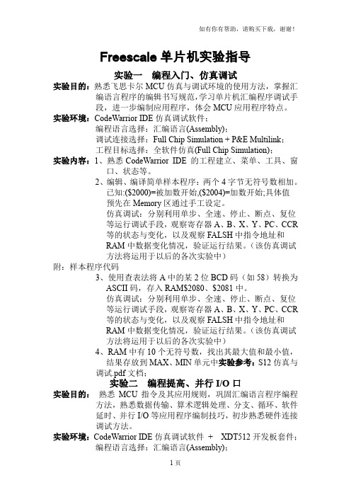
一般性实验实验一普通I/O口操作实验实验目的:1、熟悉SDIDE开发环境,熟悉GP32基本程序结构2、理解Freescale MCU的编程框架3、熟悉编程调试环境,编译、调试、下载运行第一个程序4、掌握I/O的基本编程方法范例程序:① A01_简单IO及程序框架\ FrmMain.ASM② C01_简单IO及程序框架\纯C\prgframe.prj③ C01_简单IO及程序框架\C&ASM混编\prgframe.prj实验要求:1、参看教材6.4节,熟悉实验板结构2、运行并读懂教材第7章的关于I/O口操作的LED灯控制程序3、按下列要求新建一程序:根据PB口低2位(PTB1和PTB0)的状态输出四种不同的LED显示效果,要求用最简洁的语句实现以下各效果。
(1)PTB1=0,PTB0=0时,效果为:8个LED中只有一个灯亮,亮灯顺序是从左到右,再从右到左,一个周期时间长度约4秒。
(效果1)(2)PTB1=0,PTB0=1时,效果为:8个LED中只有两个连在一起的灯亮,亮灯顺序是从左到右,再从右到左,一个周期时间长度约4秒。
(效果2)(3)PTB1=1,PTB0=0时,效果为:8个LED中只有一个灯亮,亮灯顺序是从左到右,再从右到左,一个周期时间长度约8秒。
(效果3)(4)PTB1=1,PTB0=1时,效果自定。
(效果4)实验二串行通信实验实验目的:1、理解串行通信基本原理,掌握MCU串行通信基本编程方法2、理解串行通信的查询方式和中断方式原理及其编程范例程序:1、C02_1串行通信查询方式\ H08SCI_1.prj2、C02_2串行通信中断方式\ H08SCI_2.prj3、A02_1串行通信查询方式\ SCIMain1.asm4、A02_2串行通信中断方式\ SCIMain2.asm5、以上四目录都有VB_SCI目录,该目录是对应Visual Basic6.0程序,运行在PC方,用来接收和发送数据。

飞思卡尔单片机应用实验指导书机械工程学院机械电子工程教研室实验一飞思卡尔嵌入式实验系统入门一GPIO控制实验一、头验目的:熟悉CodeWarrior集成开发环境及飞思卡尔嵌入式实验开发系统掌握AW60GPIO吉构及控制方法掌握CodeWarrior工程结构及创建汇编工程熟悉汇编指令及应用汇编语言编程方法二、实验内容1.运用CodeWarrior新建工程,进行工程程序编辑、编译、下载、调试2.利用飞思卡尔嵌入式实验开发系统根据实验需要进行硬件连接3.根据连接在PTDH上的两个拨动开关的状态,控制接中PTB口上的八个LED&在以下四种不同状态:八个LE而一灭循环;四个灯交替亮一灭;一个LE9移流水灯;两个LED&移流水灯。
实验接线原理图导线持括点*5V沏门阻挑JJ33JD J3图1-1 I/O 口实验接线图三、实验步骤1 .将飞思卡尔嵌入式实验开发系统实验箱接上电源,写入器 BDMg 头插接入核心卡BD 瞰,US 以接入 PCM USBq 。
2 . PCM 上启动CodeWarrior ,新建工程LED.mcp (注意设置工程保存路径)3 .观察工程文件结构,查看相应文件。
4 .在main.asm 中编辑工程主文件5 .编辑相关子程序6 .编译,如果有错误修改,直至编译通过7 .链接、下载,调试观察 LED 丁现象四、思考题1 . CodeWarrior 建立工程有什么工程框架文件,这些文件的作用?2 .嵌入式开发系统有哪些主要元器件?3 .如果采用模块化设计方法,将系统初始化、V VccPTB 口 PTD0 PTD1 PTD2 PTD3 PTD4 PTD5 PTD6 PTD7PTD 口导线接插点拨码开关 口 GNDLEDT 控制、延时程序等各自形成文件,导线接插点PTB0 PTB1 PTB2 PTB3 PTB4 PTB5 PTB6 PTB7工程应用这些文件时应注意什么?4.上拉电阻和下拉电阻分内置的和外接的,内置的电阻一般只有几K或十几K,外接电阻可以是几M十几Mg至更大。
目录实验一P1口输入、输出实验 (2)实验二继电器控制实验 (8)实验三音频控制实验 (11)实验四程序调试 (14)实验五5LED静态串行显示实验 (16)实验六6LED动态扫描显示实验 (21)实验七查询式键盘实验 (28)实验八阵列式键盘实验 (36)实验九计数器实验 (47)实验十定时器实验 (49)实验十一外部中断实验 (54)实验一P1口输入、输出实验一、实验目的1、学习P1口的使用方法2、学习延时子程序的编写和使用二、实验说明P1口是准双向口,它作为输出口时与一般的双向口使用方法相同。
由准双向口结构可知当P1口用作输入口时,必须先对口的锁存器写“1”,若不先对它写“1”,读入的数据是不正确的。
三、实验内容及步骤实验(一):用P1口做输出口,接八位逻辑电平显示,程序功能使发光二极管从右到左轮流循环点亮。
1、使用单片机最小应用系统1模块。
关闭该模块电源,用扁平数据线连接单片机P1口与八位逻辑电平显示模块。
2、用串行数据通信线连接计算机与仿真器,把仿真器插到模块的锁紧插座中,请注意仿真器的方向:缺口朝上。
3、打开Keil uVision2仿真软件,首先建立本实验的项目文件,接着添加P1_A.ASM源程序,进行编译,直到编译无误。
4、进行软件设置,选择硬件仿真,选择串行口,设置波特率为38400。
5、打开模块电源和总电源,点击开始调试按钮,点击RUN按钮运行程序,观察发光二极管显示情况。
发光二极管单只从右到左轮流循环点亮。
实验(二):用P1.0、P1.1作输入接两个拨断开关,P1.2、P1.3作输出接两个发光二极管。
程序读取开关状态,并在发光二极管上显示出来。
1、用导线分别连接P1.0、P1.1到两个拨断开关,P1.2、P1.3到两个发光二极管。
2、添加 P1_B.ASM源程序,编译无误后,运行程序,拨动拨断开关,观察发光二极管的亮灭情况。
向上拨为熄灭,向下拨为点亮。
四、流程图及源程序1.流程图2.源程序:(一)实验一ORG 0000HLJMP STARTORG 0030HSTART: MOV A, #0FEHMOV R2,#8OUTPUT: MOV P1,ARL AACALL DELAYDJNZ R2,OUTPUTLJMP STARTDELAY: MOV R6,#0MOV R7,#0DELAYLOOP:;延时程序DJNZ R6,DELAYLOOPDJNZ R7,DELAYLOOPRETEND(二)实验二KEYLEFT BIT P1.0 ;定义KEYRIGHT BIT P1.1LEDLEFT BIT P1.2LEDRIGHT BIT P1.3ORG 0000HLJMP STARTORG 0030HSTART: SETB KEYLEFT ;欲读先置一SETB KEYRIGHTLOOP: MOV C,KEYLEFTMOV LEDLEFT,CMOV C,KEYRIGHTMOV LEDRIGHT,CLJMP LOOPEND五、思考题(1)对于本实验延时子程序Delay: MOV R6,0MOV R7, 0DelayLoop:DJNZ R6,DelayLoopDJNZ R7,DelayLoopRET如使用12MHz晶振,粗略计算此程序的执行时间为多少?六、电路图实验二继电器控制实验一、实验目的1、学习I/O端口的使用方法2、掌握继电器的控制的基本方法3、了解用弱电控制强电的方法二、实验说明现代自动控制设备中,都存在一个电子电路的互相连接问题,一方面要使电子电路的控制信号能控制电气电路的执行元件(电动机,电磁铁,电灯等),另一方面又要为电子线路和电气电路提供良好的电气隔离,以保护电子电路和人身的安全。
第二章Freescale 8位单片机概述2.1 08系列MCU的概述Freescale的08系列单片机型号有一百多种。
在这些不同型号的单片机中,资源各不相同,即使是同一种型号的单片机,也有多种封装形式,其I/O口数目也不相同。
表4-1表现了几种08系列单片机的资源差异情况。
表4-1 08系列单片机的资源差异情况表从表4-1可以看出08系列单片机内置资源差异很大,内存容量(RAM)最大的达到4K字节,而最少的只有128个字节;最多的I/O口数有56个,最少的只有6个;闪存(FLASH)最大的达到了60K字节,而最少的只有1.5K字节。
这种差异非常适合于各种不同的应用系统。
在实际应用开发过程中,选择合适的单片机是非常重要的。
HC08系列MCU有很多类型,各种类型除了拥有HC08系列的共同特点外,又具有其自身的特点,可以满足特定的实际需求,如表4-2所示。
表4-2 MC68HC08系列MCU的类型及特点2.2 MC68HC908QY4 MCU的性能概述MC68HC908QY4是MC68HC08 微控制器系列中的产品,MC68HC08 是一种高性能的8位单片机系列,具有速度快、功能强、价格低等特点。
采用高性能的MC68HC08中央处理器与MC68HC05指令代码完全向上兼容5V或3V的工作电压(VDD)5V工作电压时内部总线频率最高为8MHZ,3V时内部总线频率最高为4MHZ8位字节可调整的内置振荡器,可产生3.2MHZ的总线频率,可调范围±5%由STOP状态可以自动唤醒通过CONFIG寄存器可以对MCU进行配置,包括低电压禁止(LVI)设置具有片内FLASH,具有FLASH存储器在线编程功能和保密功能(FLASH编程/擦除的电压由芯片内部电荷泵产生)MC68HC908QY4的FLASH的存储器大小为4096字节128字节的片内ROM双通道16位定时器模块(TIM)MC68HC908QY4具有4路8位模数转换器(ADC)13个双向I/O口,一个单向输入口:所有I/O口都具有很强的吸电流和放电流能力所有I/O口内部上拉电阻6位键盘中断,具有唤醒的特点低电压禁止模块(LVI)具有软件可选的特点,由CONFIG寄存器进行设置系统保护特性:设计算机工作正常(COP)复位低电压检测复位非法指令码检测复位非法地址检测复位IRQ),此引脚与通用输入引脚复用带有内部上拉的外部异步中断引脚(复位引脚(RST),与通用I/O复用上电复位RST和IRQ引脚的内部上拉可以降低外围路的复杂性存储器映射I/O寄存器WAIT和STOP低功耗模式MC68HC908QY4 具有以下封装:16引脚PDIP、SOIC、TSSOP2.3内部结构简图MC68HC908QY4系列结构框图如图2-1所示。
飞思卡尔单片机应用实验指导书机械工程学院机械电子工程教研室实验一飞思卡尔嵌入式实验系统入门—GPIO控制实验一、实验目的:熟悉CodeWarrior集成开发环境及飞思卡尔嵌入式实验开发系统掌握AW60的GPIO结构及控制方法掌握CodeWarrior工程结构及创建汇编工程熟悉汇编指令及应用汇编语言编程方法二、实验内容1.运用CodeWarrior新建工程,进行工程程序编辑、编译、下载、调试2.利用飞思卡尔嵌入式实验开发系统根据实验需要进行硬件连接3.根据连接在PTD口上的两个拨动开关的状态,控制接中PTB口上的八个LED处在以下四种不同状态:八个LED亮—灭循环;四个灯交替亮—灭;一个LED左移流水灯;两个LED右移流水灯。
实验接线原理图图1-1 I/O 口实验接线图三、实验步骤1.将飞思卡尔嵌入式实验开发系统实验箱接上电源,写入器BDM 接头插接入核心卡BDM 座,USB 头接入PC 机USB 口。
2.PC 机上启动CodeWarrior ,新建工程LED.mcp(注意设置工程保存路径) 3.观察工程文件结构,查看相应文件。
4.在main.asm 中编辑工程主文件 5.编辑相关子程序6.编译,如果有错误修改,直至编译通过 7.链接、下载,调试观察LED 灯现象四、思考题1.CodeWarrior 建立工程有什么工程框架文件,这些文件的作用?2.嵌入式开发系统有哪些主要元器件?3.如果采用模块化设计方法,将系统初始化、LED 灯控制、延时程序等各自形成文件,GNDPTB 口 Vcc工程应用这些文件时应注意什么?4.上拉电阻和下拉电阻分内置的和外接的,内置的电阻一般只有几K或十几K,外接电阻可以是几M、十几M甚至更大。
当要求功耗较低时,应该怎样选择内置的还是外接的电阻?5.该实验的开关通过I/O口控制小灯的程序,分别叙述断点调试和单步调试的步骤,其中包含:利用汇编语言时,注意观察寄存器值的变化并记录寄存器中每次的值实验二串口通信(SCI)实验一、实验目的:1.进一步熟悉嵌入式开发系统环境、汇编、C语言、调试方式。
单片机原理与应用技术实验指导书(Freescale)机械工程学院机械电子工程教研室王晓峰实验一飞思卡尔嵌入式实验系统入门—GPIO控制实验一、实验目的:熟悉CodeWarrior集成开发环境及飞思卡尔嵌入式实验开发系统掌握AW60的GPIO结构及控制方法掌握CodeWarrior工程结构及创建汇编工程熟悉汇编指令及应用汇编语言编程方法二、实验内容1.运用CodeWarrior新建工程,进行工程程序编辑、编译、下载、调试;2.利用飞思卡尔嵌入式实验开发系统根据实验需要进行硬件连接;3.观察示例工程项目,该工程功能为:根据连接在PTC0、PTC1口上的两个拨动开关的状态,控制接中PTB口上的八个LED处在以下二种不同状态:八个LED同时亮-灭循环;四个灯交替亮-灭;4.设计一个比示例工程简单的工程项目,内容为控制PTB口上连接的八个LED灯同时亮-灭循环一次再四个灯交替亮-灭一次。
5.设计一个比示例工程更复杂一些的工程项目,根据连接在PTC口上的两个拨动开关的状态,控制接中PTB口上的八个LED处在以下四种不同状态:八个LED亮—灭循环;四个灯交替亮—灭;一个LED左移流水灯;两个LED右移流水灯。
三、实验步骤(注意:在调试过程中如需要进行连接线路时,要先将实验箱断电,待电路连接好后再接通电源!!!)1.将飞思卡尔嵌入式实验开发系统实验箱接上电源,写入器BDM接头插接入核心卡BDM座,USB头接入PC机USB口。
2.PC机上启动CodeWarrior,新建工程LED.mcp(注意设置工程保存路径)3.观察工程文件结构,查看相应文件。
4.在main.asm中编辑工程主文件5.编辑相关子程序6.编译,如果有错误修改,直至编译通过7.链接、下载,调试观察LED灯现象导线接插点Vcc拨码开关GN图1-1 LED及拨动开关原理图四、参考程序1.主汇编程序main.asm该程序为根据PTD口的PTD0上接的拨动开关的状态控制连接在PTB口上的八个LED灯在四亮四暗状态或八个灯同时亮同时暗的状态XDEF asm_mainXREF MCUInitXREF DelayHXINCLUDE 'derivative.inc'INCLUDE 'light.inc'INCLUDE 'switch.inc'MyCode: SECTION; this assembly routine is called the C/C++ applicationasm_main:JSR MCUInitJSR Switch_InitJSR Light_InitM_Scan: JSR Switch_ReadLDA $70CMP #$01BNE M01LDA #0JSR Light_On_OffLDHX #$0fffJSR DelayHXLDA #1JSR Light_On_OffLDHX #$0fffJSR DelayHXBRA M_ScanM01: CMP #$02BNE M02JSR Light_HalfLDHX #$0fffJSR DelayHXM02: BRA M_ScanRTS ; return to caller2、LED灯构件程序light.asm;[Light.asm]小灯驱动-----------------------------------------------------* ;本文件包含: * ; (1)Light_init:定义控制小灯的MCU的I/O引脚为输出* ; (2)Light_On_Off:驱动小灯"亮","暗" * ;--------------------------------------------------------------------------------*;小灯驱动所需头文件INCLUDE 'MC9S08AW60.inc' ;MCU映像寄存器名;小灯控制引脚宏定义Light_P: equ PTBD ;灯(Light)接在PTB口Light_D: equ PTBDD ;相应的方向寄存器Lon: equ $00Loff: equ $ffLdiff: equ $0f;声明外部函数XDEF Light_Init ;小灯初始化XDEF Light_On_Off ;驱动小灯"亮","暗"XDEF Light_Half ;驱动小灯"四亮","四灭";Lightinit:定义控制小灯的MCU引脚为输出---------------------------* ;功能:定义控制小灯的MCU引脚为输出,并使小灯初始为暗* ;----------------------------------------------------------------------------------* Light_Init:LDA #$FFSTA Light_P ;设置初始时八个LED灯全灭LDA #$FFSTA Light_D ;设置LED所接PTB口为输出RTS;Light_On_Off:驱动小灯"亮","灭"---------------------------------------* ;功能:根据A的值控制小灯的亮和暗* ;---------------------------------------------------------------------------------* Light_On_Off:CMP #0BNE Light_1LDA #LonSTA Light_PBRA Light_ExitLight_1:CMP #1BNE Light_Exit ;入口非'L'/'A',程序无响应LDA #LoffSTA Light_PLight_Exit:RTS;Light_Half:驱动小灯"四亮","四灭"-------------------------------------* ;功能:根据A的值控制小灯的亮和暗* ;---------------------------------------------------------------------------------*Light_Half:LDA Light_PCMP #LdiffBNE Light_half1LDA #~LdiffSTA Light_PBRA L_exitLight_half1:LDA #LdiffSTA Light_PL_exit:RTS3、拨动开关控制程序Switch.asm;[switch.asm]开关状态输入---------------------------------------------* ;本文件包含: * ; (1)Switch_init:定义连接开关的MCU的I/O引脚为输入* ; (2)Switch_read:读取开关状态* ; (3)RAM$70保存开关状态;--------------------------------------------------------------------------------*;小灯驱动所需头文件INCLUDE 'MC9S08AW60.inc' ;MCU映像寄存器名XDEF Switch_InitXDEF Switch_Read;开关连接引脚宏定义Switch_P: equ PTCDSwitch_D: equ PTCDDS_K1: equ 0S_K2: equ 1;Switch_Init:定义连接开关的I/O为输入----------------------------------*Switch_Init:BCLR S_K1,Switch_DBCLR S_K2,Switch_DRTS;Switch_Read:读取连接开关的I/O口数据,取出开关状态------------* ;RAM$70保存开关状态* ;------------------------------------------------------------------------------------*Switch_Read:PSHALDA #0STA $70BSET S_K1,$70BSET S_K2,$70LDA Switch_PAND $70STA $70PULARTS4、延时通用程序DelayHX.asmXDEF DelayHXDelayHX:PSHA ;[A进栈](保护寄存器A)CPX #0 ;X变址寄存器中的值是否为0BEQ DelayHX_ExitDelayHX_1:LDA #200 ;延时约200*5=1000(T)------DelayHX_2:NOP ;(1T)NOP ;(1T)DBNZA DelayHX_2AIX #-1 ;(HX - 1) -> HXCPHX #0BNE DelayHX_1DelayHX_Exit:PULA ;[A出栈](恢复寄存器A)RTS;[MCUInit.asm]AW60芯片初始化子程序---------------------*;功能: *; 系统初始化设置,设置ICGC1和ICGC2寄存器,SOPT的寄存器*; 设置,由外部晶振f = 4MHz,产生内部总线时钟f = 20MHz *;入口:无*;出口:无*;------------------------------------------------------*INCLUDE 'MC9S08AW60.inc' ;MCU映像寄存器名;声明外部函数XDEF MCUInit ;芯片初始化MCUInit:PSHA ;A进栈(保护寄存器A)LDA #%01100000; |||; |||; |||; ||+------STOPE --- 允许STOP; |+-------COPT ---- long timeout 2^18; +--------COPE ---- 关看门狗STA SOPT ;系统选项寄存器(只写一次)MOV #%00110000,ICGC2; |||||||| 应该在设置ICGC1之前写MFDx; |||||||+-RFD0 \; ||||||+--RFD1 --- 分频因子R=1; |||||+---RFD2 /; ||||+----LOCRE --- 丢失时钟信号后产生一个中断信号; |||+-----MFD0 \; ||+------MFD1 --- 锁频环倍乘因子N = 10; |+-------MFD2 /; +--------LOLRE --- 锁频环失锁后产生一个中断信号(不复位) MOV #%01111000,ICGC1; |||||||x; ||||||+--LOCD ---- 允许检测时钟信号丢失Lost of Clock; |||||+---OSCSTEN - 在OFF模式下允许晶振电路; ||||+----CLKS0 \ - 选择FLL engaged external reference(FEE) ; |||+-----CLKS1 / 使用锁频环的外时钟模式; ||+------REFS ---- 使用晶振(0表示使用外时钟信号); |+-------RANGE --- 使用高频晶振(4MHz p=1) (1-1;0-64); +--------HGO ----- 低功耗;等待FLL稳定PULA ;A出栈(恢复寄存器A)RTS四、思考题1.CodeWarrior建立工程有什么工程框架文件,这些文件的作用?2.该实验采用模块化设计方法,工程框架包含哪些文件,画出其组织结构,画出主程序流程图。
Freescale单片机实验指导书物理与电子工程学院目录实验一飞思卡尔嵌入式实验系统入门—GPIO控制实验 (3)实验二串口通信(SCI)实验 (6)实验三键盘中断及LED数码块实验 (11)实验四定时器输入捕捉与输出比较功能实验............................................. 错误!未定义书签。
实验五AD转换与PWM综合实验 .............................................................. 错误!未定义书签。
实验一飞思卡尔嵌入式实验系统入门—GPIO控制实验一、实验目的:熟悉CodeWarrior集成开发环境及飞思卡尔嵌入式实验开发系统掌握AW60的GPIO结构及控制方法掌握CodeWarrior工程结构及创建汇编工程熟悉汇编指令及应用汇编语言编程方法二、实验内容1.运用CodeWarrior新建工程,进行工程程序编辑、编译、下载、调试2.利用飞思卡尔嵌入式实验开发系统根据实验需要进行硬件连接3.根据连接在PTD口上的两个拨动开关的状态,控制接中PTB口上的八个LED处在以下四种不同状态:八个LED亮—灭循环;四个灯交替亮—灭;一个LED左移流水灯;两个LED右移流水灯。
实验接线原理图图1-1 I/O 口实验接线图三、实验步骤1.将飞思卡尔嵌入式实验开发系统实验箱接上电源,写入器BDM 接头插接入核心卡BDM 座,USB 头接入PC 机USB 口。
2.PC 机上启动CodeWarrior ,新建工程LED.mcp(注意设置工程保存路径) 3.观察工程文件结构,查看相应文件。
4.在main.asm 中编辑工程主文件 5.编辑相关子程序6.编译,如果有错误修改,直至编译通过 7.链接、下载,调试观察LED 灯现象四、思考题1.CodeWarrior 建立工程有什么工程框架文件,这些文件的作用?2.嵌入式开发系统有哪些主要元器件?3.如果采用模块化设计方法,将系统初始化、LED 灯控制、延时程序等各自形成文件,GNDPTB 口 Vcc工程应用这些文件时应注意什么?4.上拉电阻和下拉电阻分内置的和外接的,内置的电阻一般只有几K或十几K,外接电阻可以是几M、十几M甚至更大。
当要求功耗较低时,应该怎样选择内置的还是外接的电阻?5.该实验的开关通过I/O口控制小灯的程序,分别叙述断点调试和单步调试的步骤,其中包含:利用汇编语言时,注意观察寄存器值的变化并记录寄存器中每次的值实验二 串口通信(SCI )实验一、实验目的:1.进一步熟悉嵌入式开发系统环境、汇编、C 语言、调试方式。
2.加强串口通信(SCI )基本原理及编程原理的理解。
3.理解C 语言工程结构,掌握运用08C 建立工程的方法。
4.分别运用查询方式、中断方式实现通信。
二、实验要求:1.仔细阅读本实验指导书。
2.复习有关的串行通信(SCI )的章节3.熟悉AW60串行通信(SCI )的工作方法及编程。
4.根据实验内容要求编写好程序,为实验做充分地准备。
实验原理图如下:三.实验设备及其连接1.PC 机一台2.飞思卡尔嵌入式实验开发系统 一台 3.串行通信线 一根 4.万用表一只四.实验内容1.理解串行通信(SCI )原理。
2.运行与理解各子程序。
PC3.主程序运行课本的样例程序。
4.编制一个查询方式通信程序。
将字符通过SCI一个一个地发送,发送完一个字符后,控制接在PTB0~PTB7的8个LED灯显示被发送字符的ASCII码。
5.编制一个中断方式通信程序。
编程要求同上一条。
五.编程提示1.按照结构要求写好编程代码和注释。
2.计算波特率,SCInInit(SCI初始化子程序)设置SCI比特率寄存器(SCInBDH,SCInBDL),设置允许SCI、正常码输出、8位数据、无校验,即设置SCI控制寄存器1(SCIxC1)相应位,设置是否允许发送与接收、是中断接收还是查询接收,即设置SCI控制寄存器2(SCIxC2)相应位。
3.查询方式通信程序的主程序主体是一个死循环,循环体中是不断检测SCI是否发送完毕,即检测SCI状态寄存器1(SCIxS1)第七位是否为1,为1则将字符的ASCII码输出到接在PTB口的LED上,并延时一会。
4.中断方式通信程序的主程序也主体是一个死循环,但该循环体是一个空循环体,所有接收和发送数据程序代码放在中断程序中,这里没有检测代码,数据开始发送和接收的条件就是中断的条件。
六.实验报告要求1.小结AW60串行通信(SCI)的原理及编程,并画出其流程图和程序代码与硬件接线图。
2.小结中断方式和查询方式的编程方法,并画出其流程图和程序代码与硬件接线图。
3.回答下列问题(1)串行SCI通信有哪些中断?各在什么情况下发生,作用是什么?(2)如何知道串行口TX发送了信号?提示:方法一,利用万用表在TX端发送0或者255持续0.5秒钟时的电压值。
方法二,在TX端发送0或255持续0.5秒钟的波形时的小灯变化。
七.参考例程:void main(void) {unsigned char SerialBuff[]="Hello! World!"; //初始化存放接收数据的数组//1 关总中断DisableInterrupts; //禁止总中断//2 芯片初始化MCUInit();//3 模块初始化SCIInit(); //串行口初始化//4 开放中断EnableInterrupts; //开放总中断SCISendN(13,SerialBuff); //串口发送“Hello World!”//5 主循环while (1){if((SCI1S1&SCI1S1_RDRF_MASK)!=0) {PTBD=SCI1D ;if((SCI1S1&SCI1S1_TDRE_MASK)!=0)SCI1D=PTBD;}elsePTBD=0x00;}}void MCUInit(void){SOPT = 0b01100000; //$70 System Options Register(write once) ICGC2 = 0b00110000; //$30 internal clock generation 2ICGC1 = 0b01111000; //$78 internal clock generation 1//等待FLL稳定while(!ICGS1_LOCK);PTBDD=0xff ;PTBD=0xff ;}void SCIInit(){unsigned int ubgs,baud=9600;unsigned char sysclk=20;//1.计算波特率并设置:ubgs = fsys/(波特率*16)(其中fsys=sysclk*1000000)ubgs = sysclk*(10000/(baud/100))/16; //理解参考上一行,此处便于CPU运算SCI1BDH= (unsigned char)((ubgs & 0xFF00) >> 8);SCI1BDL= (unsigned char)(ubgs & 0x00FF);//无校验,正常模式(开始信号+ 8位数据(先发最低位) + 停止信号)SCI1C1= 0;//允许发送,允许接收,查询方式收发SCI1C2= (0| SCI1C2_TE_MASK| SCI1C2_RE_MASK );}void SCISend1(unsigned char ch){while(!(SCI1S1 & SCI1S1_TDRE_MASK));//判断发送缓冲区是否为空SCI1D = ch;}void SCISendN(unsigned char n, unsigned char ch[]){unsigned i;for (i = 0; i < n; i++)SCISend1(ch[i]);}unsigned char SCIRe1(unsigned char *p){unsigned int k;unsigned char i;for (k = 0; k < 0x0b; k++)//有时间限制if((SCI1S1 & SCI1S1_RDRF_MASK) != 0)//判断接收缓冲区是否满{i = SCI1D;*p = 0x00;break;}if (k >= 0x0b) //接收失败{i = 0xff;*p = 0x01;}return i;}unsigned char SCIReN(unsigned n,unsigned char ch[]){unsigned char m;unsigned char fp; //接收标志m = 0;while (m < n){ch[m] = SCIRe1(&fp);if (fp == 1){return 1; //接收失败}m++;}return 0; //接收成功}实验三键盘中断及LED数码块实验一、实验目的:1.熟练运用嵌入式开发系统环境、C语言及调试方式。
2.复习串行通信接口(SCI)的内容。
3.加强键盘中断基本原理及编程原理的理解。
4.理解“行扫描”法的原理并能进行键值识别和键值编码。
5.理解键盘接线原理图(如图3-1)。
6.理解LED数码块的显示原理,初步掌握LED数码块显示编程方法。
实验箱提供一个16键键盘,用于键盘中断信号的输入。
系统提供两种接线方式:①当将键盘接入上一排插孔时为固定接线,键盘接线原理图如图3-1所示。
②当将键盘接入下一排插孔时为手动接线,连线的位置在键盘的左边。
实验箱提供四个LED数码块,PB0~PB7为段码接口,PTD0、PTD1、PTD4、PTD5为位码控制接口。
PTG0PTG1PTG2PTG3PTG4PTD2PTD3PTD7二、实验要求:1.仔细阅读本实验指导书。
2.复习有关的键盘中断和串行通信接口(SCI)的章节。
3.熟悉AW60键盘模块的工作方法及编程。
4.根据实验内容要求编写好程序,为实验做充分地准备。
三.实验设备及其连接1.PC机一台2.飞思卡尔嵌入式实验开发系统一台3.串行通信线一根四.实验内容1.理解并运行按键扫描及键值键码发送样例程序(将按键的键值及键码从串行口发送到PC机端的串口工具软件);2.编制一个中断方式的16键键盘程序,使用“行扫描”法识别按键;采用键盘中断方式。
PTD7,3,2及PTG4接键盘4根列线,PTG3-0接键盘4根行线。
要求按下的一个键的键值和键面定义值(键的ASCII码值)通过串口在PC方软件界面显示,同时用小灯显示按键的键面定义值(键的ASCII码值),PTB7-PTB0口与小灯相连;3.理解并运行LED数码块样例程序(在LED数码块上显示“2011”);4.参考按键及LED数码块样例程序,设计一个按键显示程序。