ST7MDT5-EMU2B中文资料
- 格式:pdf
- 大小:112.50 KB
- 文档页数:4


2703 drw 01PD 0PD 1– GND – GNDGND CS 3A 16I/O 16I/O 17I/O 18I/O 19A 10A 11A 12A 13I/O 20I/O 21I/O 22I/O 23GNDI/O 0I/O 1I/O 2I/O 3V CC A 7A 8A 9I/O 4I/O 5I/O 6WE I/O 7CS 1PD 0A 14CS 4A 17OE I/O 24I/O 25I/O 26I/O 27A 3A 4A 5V CC A 6I/O 28I/O 29I/O 30I/O 31PD 1GND I/O 8I/O 9I/O 10I/O 11A 0A 1A 2I/O 12I/O 13I/O 14I/O 15GND CS 2A 15(IDT7MP4145 upgradeable to 4 megabyte, IDT7MP4120)•Low profile 64 pin ZIP (Zig-zag In-line vertical Package)or 64 pin SIMM (Single In-line Memory Module) for IDT7MP4045 and 72 pin SIMM (Single In-line Memory Module) for IDT7MP4145•Very fast access time: 15ns (max.)•Surface mounted plastic components on an epoxy laminate (FR-4) substrate•Single 5V (±10%) power supply•Multiple GND pins and decoupling capacitors for maxi-mum noise immunity•Inputs/outputs directly TTL-compatible2703 tbl 01COMMERCIAL TEMPERATURE RANGESEPTEMBER 1996©1996 Integrated Device Technology, Inc.DSC-2703/7The IDT logo is a registered trademark of Integrated Device Technology Inc.NOTE:1.Pins 2 and 3 (PD 0 and PD 1) are read by the user to determine the densityof the module. If PD 0 reads GND and PD 1 reads GND, then the module has a 256K depth.constructed on an epoxy laminate (FR-4) substrate using 8256K x 4 static RAMs in plastic SOJ packages. Availability of four chip select lines (one for each group of two RAMs)provides byte access. The IDT7MP4045 is available with access time as fast as 10ns with minimal power consumption.The IDT7MP4045 is packaged in a 64 pin FR-4 ZIP (Zig-zag In-line vertical Package)or a 64 pin SIMM (Single In-line Memory Module) where as the 7MP4145 is packaged in a 72pin SIMM (Single In-line Memory Module). The 4045 ZIP configuration allows 64 pins to be placed on a package 3.65inches long and 0.365 inches wide. The 7MP4045 ZIP is only 0.585 inches high, this low profile package is ideal for systems with minimum board spacing while the SIMM configuration allows use of edge mounted sockets to secure the module.All inputs and outputs of the IDT7MP4045/4145 are TTL-compatible and operate from a single 5V supply. Full asyn-chronous circuitry requires no clocks or refresh for operation and provides equal access and cycle times for ease of use.Identification pins are provided for applications in which different density versions of the module are used. In this way,the target system can read the respective levels of PD pins to determine a 256K depth.The contact pins are plated with 100 micro-inches of nickel covered by 30 micro-inches minimum of selective gold.PIN CONFIGURATION – 7MP4045(1)FUNCTIONAL BLOCK DIAGRAMOEWE 2703 drw 02I/O 0-31PDRECOMMENDED OPERATINGTEMPERATURE AND SUPPLY VOLTAGEANOTE:2703 tbl 021.This parameter is guaranteed by design but not tested.RECOMMENDED DC OPERATING NOTE:2703 tbl 031.V IL (min) = –1.5V for pulse width less than 10ns.(1)NOTE:2703 tbl 061.Stresses greater than those listed under ABSOLUTE MAXIMUMRATINGS may cause permanent damage to the device. This is a stress rating only and functional operation of the device at these or any other conditions above those indicated in the operational sections of this specification is not implied. Exposure to absolute maximum rating conditions for extended periods may affect reliability.PIN CONFIGURATION – 7MP4145(1)SIMM TOP VIEWNOTE:1.Pins 3,4,6,and 7 (PD 0-3) are read by the user to determine the density ofthe module. If PD 0, PD 1 read GND and PD 2, PD 3 read OPEN, then the module has a 256K depth.1 3 5 7 91113151719212325272931333537394143454749515355575961636567697124681012141618202224262830323436384042444648505254565860626466687072NC PD 2GND PD 1I/O 8I/O 9I/O 10I/O 11A 0A 1A 2I/O 12I/O 13I/O 14I/O 15GND A 15CS 2CS 4A 17OE I/O 24I/O 25I/O 26I/O 27A 3A 4A 5V CC A 6I/O 28I/O 29I/O 30I/O 31NC NCNC PD 3PD 0I/O 0I/O 1I/O 2I/O 3V CC A 7A 8A 9I/O 4I/O 5I/O 6I/O 7WE A 14CS 1CS 3A 16GND I/O 16I/O 17I/O 18I/O 19A 10A 11A 12A 13I/O 20I/O 21I/O 22I/O 23GND NC NCPD 0 - GND PD 1 - GND PD 2 - OPEN PD 3 - OPEN2703 drw 15Figure 1. Output Load*Includes scope and jig.Figure 2. Output Load(for t OLZ ,t OHZ , t CHZ , t CLZ , t WHZ , t OW )+5 V480 Ω30 pF*DATA OUT255Ω2703 drw 03+5 V480 Ω5 pF*DATA OUT255Ω2703 drw 042703 tbl 092703 tbl2703 tbl 07DC ELECTRICAL CHARACTERISTICSAC ELECTRICAL CHARACTERISTICSNOTE:2703 tbl 11 1.This parameter is guaranteed by design but not tested.TIMING WAVEFORM OF READ CYCLE NO. 1(1)TIMING WAVEFORM OF READ CYCLE NO. 2(1,2,4)TIMING WAVEFORM OF READ CYCLE NO. 3(1,3,4)OEADDRESSCSDATA OUT2703 drw 072703 drw 08DATA OUTADDRESS2703 drw 06DATA OUTCSNOTES:1.WE is HIGH for Read Cycle.2.Device is continuously selected. CS = V IL .3.Address valid prior to or coincident with CS transition LOW.4.OE = V IL .5.Transition is measured ±200mV from steady state. This parameter is guaranteed by design, but not tested.CSDATA INADDRESSWEDATA OUTOETIMING WAVEFORM OF WRITE CYCLE NO. 1 (WE CONTROLLED) (1, 2, 3, 7)CS2703 drw 11DATA INADDRESSWETIMING WAVEFORM OF WRITE CYCLE NO. 2 (CS CONTROLLED) (1, 2, 3, 5)NOTES:1.WE or CS must be HIGH during all address transitions.2. A write occurs during the overlap (t WP ) of a LOW CS and a LOW WE .3.t WR is measured from the earlier of CS or WE going HIGH to the end of write cycle.4.During this period, I/O pins are in the output state, and input signals must not be applied.5.If the CS LOW transition occurs simultaneously with or after the WE LOW transition, the outputs remain in a high-impedance state.6.Transition is measured ±200mV from steady state with a 5pF load (including scope and jig). This parameter is guaranteed by design, but not tested.7.If OE is LOW during a WE controlled write cycle, the write pulse width must be the larger of t WP or (t WHZ + t DW ) to allow the I/O drivers to turn off and datato be placed on the bus for the required t DW . If OE is HIGH during a WE controlled write cycle, this requirement does not apply and the write pulse can be as short as the specified t WP .PACKAGE DIMENSIONS 7MP4045 ZIP VERSION2703 drw 137MP4045 SIMM VERSION2703 drw 12SIDE VIEWORDERING INFORMATION7MP4145 SIMM VERSION2703 drw 16X PowerX SpeedX PackageX Process/Commercial (0°C to +70°C)Z MFR-4 ZIP (Zig-Zag In-line vertical Package,7MP4045 only)FR-4 SIMM (Single In-line Memory Module)XXXXXDevice IDT Speed in NanosecondsS Standard Power7MP40457MP4145256K x 32 Static RAM Module 256K x 32 Static RAM Module2703 drw 14。


Information their respective owners.Rev. Gfurnished by Analog Devices is believed to be accurate and reliable. However , no responsibility is assumed by Analog Devices for its use, nor for any infringements of patents or other rights of third parties that may result from its use. Speci cations subject to change without notice. No license is granted by implication or otherwise under any patent or patent rights of Analog Devices. T rademarks and registered trademarks are the property ofOne Technology Way, P.O. Box 9106, Norwood, MA 02062-9106, U.S.A.Tel: 781.329.4700 Fax: 781.461.3113 ©2000–2011 Analog Devices, Inc. All rights reserved.引脚配置01525-001OUT A 1V–2+IN 3V+5–IN4AD8601TOP VIEW (Not to Scale)图1. 5引脚SOT-23(RJ 后缀)OUT A 1–IN A 2+IN A 3V–4V+8OUT B 7–IN B6+IN B5AD8602TOP VIEW (Not to Scale)01525-002图2. 8引脚MSOP(RM 后缀)和8引脚SOIC(R 后缀)01525-0031234567AD8604–IN A +IN A V+OUT B –IN B +IN B OUT A 141312111098–IN D +IN D V–OUT C–IN C +IN C OUT D TOP VIEW (Not to Scale)图3. 14引脚TSSOP(RU 后缀)和14引脚SOIC(R 后缀)12345678161514131211109–IN A +IN A V+OUT B–IN B +IN B OUT A –IN D+IN D V–OUT CNCNCNC = NO CONNECT–IN C +IN C OUT D TOP VIEW (Not to Scale)AD860401525-004图4. 16引脚紧缩小型封装QSOP(RQ 后缀)ADI 中文版数据手册是英文版数据手册的译文,敬请谅解翻译中可能存在的语言组织或翻译错误,ADI 不对翻译中存在的差异或由此产生的错误负责。


ST7MDT1-DVP2中⽂资料Rev.2.2February 20001/135This is preliminary information on a new product in development or undergoing evaluation.Details are subject to change without notice. ST72104G,ST72215G,ST72216G,ST72254G8-BIT MCU WITH SINGLE VOLT AGE FLASH MEMORY ,ADC,16-BIT TIMERS,SPI,I 2C INTERFACESPRELIMINARY DATAsMemories–4K or 8K bytes Program memory (ROM and single voltage FLASH)with read-out protec-tion and in-situ programming (remote ISP)–256bytes RAMsClock,Reset and Supply Management –Enhanced reset system–Enhanced low voltage supply supervisor with 3programmable levels–Clock sources:crystal/ceramic resonator os-cillators or RC oscillators,external clock,backup Clock Security System –Clock-out capability–3Power Saving Modes:Halt,Wait and Slow sInterrupt Management–7interrupt vectors plus TRAP and RESET –22external interrupt lines (on 2vectors)s22I/O Ports–22multifunctional bidirectional I/O lines –14alternate function lines –8high sink outputs s3Timers–Configurable watchdog timer–Two 16-bit timers with:2input captures,2out-put compares,external clock input on one tim-er,PWM and Pulse generator modes (one only on ST72104Gx and ST72216G1)s2Communications Interfaces –SPI synchronous serial interface –I2C multimaster interface (only on ST72254Gx)s1Analog peripheral–8-bit ADC with 6input channels (except on ST72104Gx)sInstruction Set–8-bit data manipulation –63basic instructions–17main addressing modes–8x 8unsigned multiply instruction –True bit manipulationsDevelopment Tools–Full hardware/software development packageDevice SummarySDIP32SO28FeaturesST72104G1ST72104G2ST72216G1ST72215G2ST72254G1ST72254G2Program memory -bytes 4K8K4K8K4K8KRAM (stack)-bytes 256(128)PeripheralsWatchdog timer,One 16-bit timer,SPIWatchdog timer,One 16-bit timer,SPI,ADC Watchdog timer,Two 16-bit timers,SPI,ADCWatchdog timer,Two 16-bit timers,SPI,I C,ADCOperating Supply 3.0V to 5.5VCPU FrequencyUp to 8MHz (with oscillator up to 16MHz)Operating Temperature -40°C to +85°C (-40°C to +105/125°C optional)PackagesSO28/SDIP321元器件交易⽹/doc/6b622d52be23482fb4da4cc6.htmlTable of Contents1352/13521INTRODUCTION ..............................................................62PIN DESCRIPTION ............................................................73REGISTER&MEMORY MAP (104)FLASH PROGRAM MEMORY ..................................................134.1INTRODUCTION .......................................................134.2MAIN FEATURES ......................................................134.3STRUCTURAL ORGANISATION ..........................................134.4IN-SITU PROGRAMMING (ISP)MODE (13)4.5MEMORY READ-OUT PROTECTION ......................................135CENTRAL PROCESSING UNIT . (14)5.1INTRODUCTION .......................................................145.2MAIN FEATURES ......................................................145.3CPU REGISTERS (14)6SUPPLY,RESET AND CLOCK MANAGEMENT ....................................176.1LOW VOLTAGE DETECTOR (LVD)........................................186.2RESET SEQUENCE MANAGER (RSM).....................................196.2.1Introduction .......................................................196.2.2Asynchronous External RESET pin .....................................206.2.3Internal Low Voltage Detection RESET ..................................206.2.4Internal Watchdog RESET ............................................206.3MULTI-OSCILLATOR (MO)...............................................216.4CLOCK SECURITY SYSTEM (CSS) (22)6.4.1Clock Filter Control .................................................226.4.2Safe Oscillator Control ...............................................226.4.3Low Power Modes .................................................226.4.4Interrupts .........................................................226.5CLOCK RESET AND SUPPLY REGISTER DESCRIPTION (CRSR) (23)6.6MAIN CLOCK CONTROLLER (MCC) (24)7INTERRUPTS ...............................................................257.1NON MASKABLE SOFTWARE INTERRUPT .................................257.2EXTERNAL INTERRUPTS ...............................................257.3PERIPHERAL INTERRUPTS (25)8POWER SAVING MODES .....................................................278.1INTRODUCTION .......................................................278.2SLOW MODE .........................................................278.3WAIT MODE ..........................................................288.4HALT MODE (29)9I/O PORTS ..................................................................309.1INTRODUCTION .......................................................309.2FUNCTIONAL DESCRIPTION ............................................309.2.1Input Modes .......................................................309.2.2Output Modes .....................................................309.2.3Alternate Functions .................................................309.3I/O PORT IMPLEMENTATION ............................................33元器件交易⽹/doc/6b622d52be23482fb4da4cc6.html元器件交易⽹/doc/6b622d52be23482fb4da4cc6.htmlTable of Contents9.4LOW POWER MODES (34)9.5INTERRUPTS (34)9.6REGISTER DESCRIPTION (34)10MISCELLANEOUS REGISTERS (36)10.1I/O PORT INTERRUPT SENSITIVITY (36)10.2I/O PORT ALTERNATE FUNCTIONS (36)10.3MISCELLANEOUS REGISTER DESCRIPTION (37)11ON-CHIP PERIPHERALS (39)11.1WATCHDOG TIMER(WDG) (39)11.1.1Introduction (39)11.1.2Main Features (39)11.1.3Functional Description (39)11.1.4Hardware Watchdog Option (40)11.1.5Low Power Modes (40)11.1.6Interrupts (40)11.1.7Register Description (40)11.216-BIT TIMER (42)11.2.1Introduction (42)11.2.2Main Features (42)11.2.3Functional Description (42)11.2.4Low Power Modes (54)11.2.5Interrupts (54)11.2.6Summary of Timer modes (54)11.2.7Register Description (55)11.3SERIAL PERIPHERAL INTERFACE(SPI) (60)11.3.1Introduction (60)11.3.2Main Features (60)11.3.3General description (60)11.3.4Functional Description (62)11.3.5Low Power Modes (69)11.3.6Interrupts (69)11.3.7Register Description (70)11.4I2C BUS INTERFACE(I2C) (73)11.4.1Introduction (73)11.4.2Main Features (73)11.4.3General Description (73)11.4.4Functional Description (75)11.4.5Low Power Modes (79)11.4.6Interrupts (79)11.4.7Register Description (80)11.58-BIT A/D CONVERTER(ADC) (86)11.5.1Introduction (86)11.5.2Main Features (86)11.5.3Functional Description (86)11.5.4Low Power Modes (87)11.5.5Interrupts (87)11.5.6Register Description (88)3/1353元器件交易⽹/doc/6b622d52be23482fb4da4cc6.html ST72104G,ST72215G,ST72216G,ST72254G12INSTRUCTION SET (90)12.1ST7ADDRESSING MODES (90)12.1.1Inherent (91)12.1.2Immediate (91)12.1.3Direct (91)12.1.4Indexed(No Offset,Short,Long) (91)12.1.5Indirect(Short,Long) (91)12.1.6Indirect Indexed(Short,Long) (92)12.1.7Relative mode(Direct,Indirect) (92)12.2INSTRUCTION GROUPS (93)13ELECTRICAL CHARACTERISTICS (96)13.1PARAMETER CONDITIONS (96)13.1.1Minimum and Maximum values (96)13.1.2Typical values (96)13.1.3Typical curves (96)13.1.4Loading capacitor (96)13.1.5Pin input voltage (96)13.2ABSOLUTE MAXIMUM RATINGS (97)13.2.1Voltage Characteristics (97)13.2.2Current Characteristics (97)13.2.3Thermal Characteristics (97)13.3OPERATING CONDITIONS (98)13.3.1General Operating Conditions (98)13.3.2Operating Conditions with Low Voltage Detector(LVD) (99) 13.4SUPPLY CURRENT CHARACTERISTICS (101)13.4.1RUN and SLOW Modes (101)13.4.2WAIT and SLOW WAIT Modes (102)13.4.3HALT Mode (103)13.4.4Supply and Clock Managers (103)13.4.5On-Chip Peripherals (103)13.5CLOCK AND TIMING CHARACTERISTICS (104)13.5.1General Timings (104)13.5.2External Clock Source (104)13.5.3Crystal and Ceramic Resonator Oscillators (105)13.5.4RC Oscillators (106)13.5.5Clock Security System(CSS) (107)13.6MEMORY CHARACTERISTICS (108)13.6.1RAM and Hardware Registers (108)13.6.2FLASH Program Memory (108)13.7EMC CHARACTERISTICS (109)13.7.1Functional EMS (109)13.7.2Absolute Electrical Sensitivity (110)13.7.3ESD Pin Protection Strategy (112)13.8I/O PORT PIN CHARACTERISTICS (114)13.8.1General Characteristics (114)13.8.2Output Driving Current (115)13.9CONTROL PIN CHARACTERISTICS (117)4/135元器件交易⽹/doc/6b622d52be23482fb4da4cc6.htmlST72104G,ST72215G,ST72216G,ST72254G13.9.1Asynchronous RESET Pin (117)13.9.2ISPSEL Pin (119)13.10TIMER PERIPHERAL CHARACTERISTICS (120)13.10.1Watchdog Timer (120)13.10.216-Bit Timer (120)13.11COMMUNICATION INTERFACE CHARACTERISTICS (121)13.11.1SPI-Serial Peripheral Interface (121)13.11.2I2C-Inter IC Control Interface (123)13.128-BIT ADC CHARACTERISTICS (124)14PACKAGE CHARACTERISTICS (126)14.1PACKAGE MECHANICAL DATA (126)14.2THERMAL CHARACTERISTICS (127)14.3SOLDERING AND GLUEABILITY INFORMATION (128)14.4PACKAGE/SOCKET FOOTPRINT PROPOSAL (128)15DEVICE CONFIGURATION AND ORDERING INFORMATION (129)15.1OPTION BYTES (129)15.2DEVICE ORDERING INFORMATION AND TRANSFER OF CUSTOMER CODE (130)15.3DEVELOPMENT TOOLS (132)15.4ST7APPLICATION NOTES (133)15.5TO GET MORE INFORMATION (133)16SUMMARY OF CHANGES (134)5/135ST72104G,ST72215G,ST72216G,ST72254G6/1351INTRODUCTIONThe ST72104G,ST72215G,ST72216G and ST72254G devices are members of the ST7mi-crocontroller family.They can be grouped as fol-lows:–ST72254G devices are designed for mid-range applications with ADC and I C interface capabili-ties.–ST72215/6G devices target the same range of applications but without I C interface.–ST72104G devices are for applications that do not need ADC and I C peripherals.All devices are based on a common industry-standard 8-bit core,featuring an enhanced instruc-tion set.The ST72C104G,ST72C215G,ST72C216G and ST72C254G versions feature single-voltage FLASH memory with byte-by-byte In-Situ Pro-gramming (ISP)capability.Under software control,all devices can be placed in WAIT,SLOW,or HALT mode,reducing power consumption when the application is in idle or standby state.The enhanced instruction set and addressing modes of the ST7offer both power and flexibility to software developers,enabling the design of highly efficient and compact application code.In addition to standard 8-bit data management,all ST7micro-controllers feature true bit manipulation,8x8un-signed multiplication and indirect addressing modes.For easy reference,all parametric data are located in Section 13on page 96.Figure 1.General Block Diagram8-BIT COREALU ADDRESS AND DATA BUSOSC1OSC2RESETPORT B 16-BIT TIMER APORT ASPI PORT C 8-BIT ADC WATCHDOGPB7:0(8bits)PC5:0(6bits)MULTI OSC Internal CLOCKCONTROL RAM (256Bytes)PA7:0(8bits)V SS V DD POWER SUPPLY16-BIT TIMER BPROGRAM (4or 8K Bytes)LVD+CLOCK FILTERI 2C MEMORY 4元器件交易⽹/doc/6b622d52be23482fb4da4cc6.htmlST72104G,ST72215G,ST72216G,ST72254G7/1352PIN DESCRIPTIONFigure 2.28-Pin SO Package PinoutFigure 3.32-Pin SDIP Package Pinout15161718192028272625242322211234567891011121314RESET OSC1AIN3/ICAP2_B/PC3AIN4/OCMP2_B/PC4AIN5/EXTCLK_A/PC5ICAP1_A/PB0OCMP1_A/PB1ICAP2_A/PB2OCMP2_A/PB3MOSI/PB4ISPDATA/MISO/PB5 ISPCLK/SCK/PB6SS/PB7OSC2V DD V SSPC2/MCO/AIN2PC1/OCMP1_B/AIN1PC0/ICAP1_B/AIN0PA7(HS)PA6(HS)/SDAI PA5(HS)PA4(HS)/SCLI PA3(HS)PA2(HS)PA1(HS)PA0(HS)ISPSEL ei1ei0ei0or ei1(HS)20mA high sink capabilityeiX associated external interrupt vector2827262524232221201918171615123456789101112131429303132RESET OSC1AIN3/ICAP2_B/PC3AIN4/OCMP2_B/PC4AIN5/EXTCLK_A/PC5ICAP1_A/PB0OCMP1_A/PB1ICAP2_A/PB2OCMP2_A/PB3MOSI/PB4ISPDATA/MISO/PB5ISPCLK/SCK/PB6SS/PB7OSC2NCNCV DD V SS PC2/MCO/AIN2PC1/OCMP1_B/AIN1PC0/ICAP1_B/AIN0PA7(HS)PA6(HS)/SDAI PA5(HS)PA4(HS)/SCLI PA3(HS)PA2(HS)PA1(HS)PA0(HS)ISPSEL NCNCei1ei0ei0ei1ei0orei1(HS)20mA high sink capabilityeiX associated external interrupt vector5元器件交易⽹/doc/6b622d52be23482fb4da4cc6.htmlST72104G,ST72215G,ST72216G,ST72254G8/135PIN DESCRIPTION (Cont’d)For external pin connection guidelines,refer to Section 13”ELECTRICAL CHARACTERISTICS”on page 96.Legend /Abbreviations for Table 1:Type:I =input,O =output,S =supply Input level:A =Dedicated analog input In/Output level:C =CMOS0.3V DD /0.7V DD ,C T =CMOS 0.3V DD /0.7V DD with input triggerOutput level:HS =20mA high sink (on N-buffer only)Port and control configuration:–Input:float =floating,wpu =weak pull-up,int =interrupt 1),ana =analog –Output:OD =open drain 2),PP =push-pullRefer to Section 9”I/O PORTS”on page 30for more details on the software configuration of the I/O ports.The RESET configuration of each pin is shown in bold.This configuration is valid as long as the device is in reset state.Table 1.Device Pin DescriptionPin n °Pin NameT y p eLevelPort /Control Main Function (after reset)Alternate FunctionS D I P 32S O 28I n p u tO u t p u t Input Output f l o a tw p ui n ta n a O DP P11RESET I/O C T X X Top priority non maskable interrupt (active low)22OSC13)I External clock input or Resonator oscillator in-verter input or resistor input for RC oscillator 33OSC23)O Resonator oscillator inverter output or capaci-tor input for RC oscillator44PB7/SSI/O C T X ei1X X Port B7SPI Slave Select (active low)55PB6/SCK/ISPCLK I/O C T X ei1X X Port B6SPI Serial Clock or ISP Clock 66PB5/MISO/ISPDATA I/O C T X ei1X X Port B5SPI Master In/Slave Out Data or ISP Data77PB4/MOSII/OC TXei1XXPort B4SPI Master Out /Slave In Data8NC Not Connected9NC108PB3/OCMP2_A I/O C T X ei1X X Port B3Timer A Output Compare 2119PB2/ICAP2_A I/O C T X ei1X X Port B2Timer A Input Capture 21210PB1/OCMP1_A I/O C T X ei1X X Port B1Timer A Output Compare 11311PB0/ICAP1_AI/OC T X ei1X X Port B0Timer A Input Capture 11412PC5/EXTCLK_A/AIN5I/O C T X ei0/ei1X X Port C5Timer A Input Clock or ADC Analog Input 51513PC4/OCMP2_B/AIN4I/O C T X ei0/ei1X X Port C4Timer B Output Compare 2or ADC Analog Input 41614PC3/ICAP2_B/AIN3I/O C T X ei0/ei1X X X Port C3Timer B Input Capture 2or ADC Analog Input 31715PC2/MCO/AIN2I/OC TXei0/ei1XXXPort C2Main clock output (f CPU )or ADC Analog Input 26元器件交易⽹/doc/6b622d52be23482fb4da4cc6.htmlST72104G,ST72215G,ST72216G,ST72254G9/135Notes :1.In the interrupt input column,“eiX”defines the associated external interrupt vector.If the weak pull-up column (wpu)is merged with the interrupt column (int),then the I/O configuration is pull-up interrupt input,else the configuration is floating interrupt input.2.In the open drain output column,“T”defines a true open drain I/O (P-Buffer and protection diode to V DD are not implemented).See Section 9”I/O PORTS”on page 30and Section 13.8”I/O PORT PIN CHAR-ACTERISTICS”on page 114for more details.3.OSC1and OSC2pins connect a crystal or ceramic resonator,an external RC,or an external source to the on-chip oscillator see Section 2”PIN DESCRIPTION”on page 7and Section 13.5”CLOCK AND TIM-ING CHARACTERISTICS”on page 104for more details.1816PC1/OCMP1_B/AIN1I/O C T X ei0/ei1X X X Port C1Timer B Output Compare 1or ADC Analog Input 11917PC0/ICAP1_B/AIN0I/OC TX ei0/ei1XX X Port C0Timer B Input Capture 1or ADC Analog Input 02018PA7I/O C T HS X ei0X XPort A72119PA6/SDAI I/O C T HS X ei0T Port A6I 2C Data 2220PA5I/O C T HS X ei0X XPort A52321PA4/SCLI I/O C T HSXei0TPort A4I 2C Clock 24NC Not Connected25NC2622PA3I/O C T HS X ei0X X Port A32723PA2I/O C T HS X ei0X X Port A22824PA1I/O C T HS X ei0X X Port A12925PA0I/O C T HS X ei0XXPort A03026ISPSEL I CXIn situ programming selection (Should be tied low in standard user mode).3127V SS S Ground3228V DDSMain power supplyPin n °Pin NameT y p eLevelPort /Control Main Function (after reset)Alternate FunctionS D I P 32S O 28I n p u tO u t p u t Input Output f l o a tw p ui n ta n a O DP P元器件交易⽹/doc/6b622d52be23482fb4da4cc6.htmlST72104G,ST72215G,ST72216G,ST72254G10/1353REGISTER &MEMORY MAPAs shown in the Figure 4,the MCU is capable of addressing 64K bytes of memories and I/O regis-ters.The available memory locations consist of 128bytes of register location,256bytes of RAM and up to 8Kbytes of user program memory.The RAM space includes up to 128bytes for the stack from 0100h to 017Fh.The highest address bytes contain the user reset and interrupt vectors.IMPORTANT:Memory locations marked as “Re-served”must never be accessed.Accessing a re-seved area can have unpredicable effects on the device.Figure 4.Memory Map0000h Program Memory (4K,8KBytes)Interrupt &Reset Vectors HW Registers DFFFh 0080h007Fh (see Table 2)E000hFFDFh FFE0h FFFFh(see Table 5on page 26)0180hReserved017Fh Short Addressing RAM0100h017Fh0080h00FFh 256Bytes RAM4KBytesF000h E000h8KBytesFFFF hZero page (128Bytes)Stack or16-bit Addressing RAM(128Bytes)元器件交易⽹/doc/6b622d52be23482fb4da4cc6.html ST72104G,ST72215G,ST72216G,ST72254G11/135Table 2.Hardware Register MapAddress BlockRegister Label Register NameReset Status Remarks 0000h 0001h 0002h Port CPCDR PCDDR PCORPort C Data RegisterPort C Data Direction Register Port C Option Register00h 1)00h 00hR/W 2)R/W 2)R/W 2)0003h Reserved (1Byte)0004h 0005h 0006h Port BPBDR PBDDR PBORPort B Data RegisterPort B Data Direction Register Port B Option Register00h 1)00h 00hR/W R/W R/W.0007h Reserved (1Byte)0008h 0009h 000Ah Port APADR PADDR PAORPort A Data RegisterPort A Data Direction Register Port A Option Register00h 1)00h 00hR/W R/W R/W000Bh to 001Fh Reserved (21Bytes)0020h MISCR1Miscellaneous Register 100h R/W 0021h 0022h 0023h SPI SPIDR SPICR SPISR SPI Data I/O Register SPI Control Register SPI Status Register xxh 0xh 00h R/W R/WRead Only 0024h WATCHDOGWDGCR Watchdog Control Register7FhR/W0025h CRSRClock,Reset,Supply Control /Status Register 000x 000x R/W0026h 0027h Reserved (2bytes)0028h 0029h 002Ah 002Bh 002Ch 002Dh 002Eh I 2CI2CCR I2CSR1I2CSR2I2CCCR I2COAR1I2COAR2I2CDRControl Register Status Register 1Status Register 2Clock Control Register Own Address Register 1Own Address Register 2Data Register00h 00h 00h 00h 00h 00h 00hR/WRead Only Read Only R/W R/W R/W R/W002Fh to 0030hReserved (4Bytes)元器件交易⽹/doc/6b622d52be23482fb4da4cc6.htmlST72104G,ST72215G,ST72216G,ST72254G12/135Legend :x=undefined,R/W=read/write Notes :1.The contents of the I/O port DR registers are readable only in output configuration.In input configura-tion,the values of the I/O pins are returned instead of the DR register contents.2.The bits associated with unavailable pins must always keep their reset value.0031h 0032h 0033h 0034h 0035h 0036h 0037h 0038h 0039h 003Ah 003Bh 003Ch 003Dh 003Eh 003Fh TIMER ATACR2TACR1TASR TAIC1HR TAIC1LR TAOC1HR TAOC1LR TACHR TACLR TAACHR TAACLR TAIC2HR TAIC2LR TAOC2HR TAOC2LR Timer A Control Register 2Timer A Control Register 1Timer A Status RegisterTimer A Input Capture 1High Register Timer A Input Capture 1Low Register Timer A Output Compare 1High Register Timer A Output Compare 1Low Register Timer A Counter High Register Timer A Counter Low RegisterTimer A Alternate Counter High Register Timer A Alternate Counter Low Register Timer A Input Capture 2High Register Timer A Input Capture 2Low Register Timer A Output Compare 2High Register TimerA Output Compare 2Low Register00h 00h xxh xxh xxh 80h 00h FFh FCh FFh FCh xxh xxh 80h 00h R/W R/W Read Only Read Only Read OnlyR/W R/W Read Only Read Only Read Only Read Only Read Only Read OnlyR/W R/W 0040h MISCR2Miscellaneous Register 200h R/W 0041h 0042h 0043h 0044h 0045h 0046h 0047h 0048h 0049h 004Ah 004Bh 004Ch 004Dh 004Eh 004Fh TIMER BTBCR2TBCR1TBSR TBIC1HR TBIC1LR TBOC1HR TBOC1LR TBCHR TBCLR TBACHR TBACLR TBIC2HR TBIC2LR TBOC2HR TBOC2LRTimer B Control Register 2Timer B Control Register 1Timer B Status RegisterTimer B Input Capture 1High Register Timer B Input Capture 1Low Register Timer B Output Compare 1High Register Timer B Output Compare 1Low Register Timer B Counter High Register Timer B Counter Low RegisterTimer B Alternate Counter High Register Timer B Alternate Counter Low Register Timer B Input Capture 2High Register Timer B Input Capture 2Low Register Timer B Output Compare 2High Register TimerB Output Compare 2Low Register00h 00h xxh xxh xxh 80h 00h FFh FCh FFh FCh xxh xxh 80h 00hR/W R/W Read Only Read Only Read OnlyR/W R/W Read Only Read Only Read Only Read Only Read Only Read OnlyR/W R/W0050h to 006Fh Reserved (32Bytes)0070h 0071h ADCADCDR ADCCSR Data RegisterControl/Status Register00h 00h Read Only R/W0072h to 007FhReserved (14Bytes)Address BlockRegister Label Register NameReset Status Remarks 元器件交易⽹/doc/6b622d52be23482fb4da4cc6.htmlST72104G,ST72215G,ST72216G,ST72254G13/1354FLASH PROGRAM MEMORY4.1INTRODUCTIONFLASH devices have a single voltage non-volatile FLASH memory that may be programmed in-situ (or plugged in a programming tool)on a byte-by-byte basis.4.2MAIN FEATURESs Remote In-Situ Programming (ISP)modes Up to 16bytes programmed in the same cycle s MTP memory (Multiple Time Programmable)sRead-out memory protection against piracy4.3STRUCTURAL ORGANISATIONThe FLASH program memory is organised in a single 8-bit wide memory block which can be used for storing both code and data constants.The FLASH program memory is mapped in the up-per part of the ST7addressing space and includes the reset and interrupt user vector area .4.4IN-SITU PROGRAMMING (ISP)MODE The FLASH program memory can be programmed using Remote ISP mode.This ISP mode allows the contents of the ST7program memory to be up-dated using a standard ST7programming tools af-ter the device is mounted on the application board.This feature can be implemented with a minimum number of added components and board area im-pact.An example Remote ISP hardware interface to the standard ST7programming tool is described be-low.For more details on ISP programming,refer to the ST7Programming Specification.Remote ISP OverviewThe Remote ISP mode is initiated by a specific se-quence on the dedicated ISPSEL pin.The Remote ISP is performed in three steps:–Selection of the RAM execution mode –Download of Remote ISP code in RAM–Execution of Remote ISP code in RAM to pro-gram the user program into the FLASH Remote ISP hardware configurationIn Remote ISP mode,the ST7has to be supplied with power (V DD and V SS )and a clock signal (os-cillator and application crystal circuit for example).This mode needs five signals (plus the V DD signal if necessary)to be connected to the programming tool.This signals are:–RESET:device reset–V SS :device ground power supply –ISPCLK:ISP output serial clock pin –ISPDATA:ISP input serial data pin–ISPSEL:Remote ISP mode selection.This pin must be connected to V SS on the application board through a pull-down resistor.If any of these pins are used for other purposes on the application,a serial resistor has to be imple-mented to avoid a conflict if the other device forces the signal level.Figure 5shows a typical hardware interface to a standard ST7programming tool.For more details on the pin locations,refer to the device pinout de-scription.Figure 5.Typical Remote ISP Interface4.5MEMORY READ-OUT PROTECTION The read-out protection is enabled through an op-tion bit.For FLASH devices,when this option is selected,the program and data stored in the FLASH memo-ry are protected against read-out piracy (including a re-write protection).When this protection option is removed the entire FLASH program memory is first automatically erased.However,the E 2PROM data memory (when available)can be protected only with ROM devices.ISPSELV SS RESETISPCLK ISPDATAO S C 1O S C 2V D DST7HE10CONNECTOR TYPE TO PROGRAMMING TOOL10K ?C L0C L1APPLICATION47K ?1XTAL元器件交易⽹/doc/6b622d52be23482fb4da4cc6.htmlST72104G,ST72215G,ST72216G,ST72254G14/1355CENTRAL PROCESSING UNIT5.1INTRODUCTIONThis CPU has a full 8-bit architecture and contains six internal registers allowing efficient 8-bit data manipulation.5.2MAIN FEATURES s 63basic instructionss Fast 8-bit by 8-bit multiply s 17main addressing modes s Two 8-bit index registers s 16-bit stack pointer s Low power modess Maskable hardware interrupts sNon-maskable software interrupt5.3CPU REGISTERSThe 6CPU registers shown in Figure 6are not present in the memory mapping and are accessed by specific instructions.Accumulator (A)The Accumulator is an 8-bit general purpose reg-ister used to hold operands and the results of the arithmetic and logic calculations and to manipulate data.Index Registers (X and Y)In indexed addressing modes,these 8-bit registers are used to create either effective addresses or temporary storage areas for data manipulation.(The Cross-Assembler generates a precede in-struction (PRE)to indicate that the following in-struction refers to the Y register.)The Y register is not affected by the interrupt auto-matic procedures (not pushed to and popped from the stack).Program Counter (PC)The program counter is a 16-bit register containing the address of the next instruction to be executed by the CPU.It is made of two 8-bit registers PCL (Program Counter Low which is the LSB)and PCH (Program Counter High which is the MSB).Figure 6.CPU RegistersACCUMULATORX INDEX REGISTERY INDEX REGISTERSTACK POINTERCONDITION CODE REGISTERPROGRAM COUNTER701C11H IN Z RESET VALUE =RESET VECTOR @FFFEh-FFFFh7707007158PCHPCL1587RESET VALUE =STACK HIGHER ADDRESSRESET VALUE =1X11X 1X X RESET VALUE =XXh RESET VALUE =XXh RESET VALUE =XXhX =Undefined Value元器件交易⽹/doc/6b622d52be23482fb4da4cc6.htmlST72104G,ST72215G,ST72216G,ST72254G15/135CPU REGISTERS (Cont’d)CONDITION CODE REGISTER (CC)Read/WriteReset Value:111x1xxxThe 8-bit Condition Code register contains the in-terrupt mask and four flags representative of the result of the instruction just executed.This register can also be handled by the PUSH and POP in-structions.These bits can be individually tested and/or con-trolled by specific instructions.Bit 4=H Half carry .This bit is set by hardware when a carry occurs be-tween bits 3and 4of the ALU during an ADD or ADC instruction.It is reset by hardware during the same instructions.0:No half carry has occurred.1:A half carry has occurred.This bit is tested using the JRH or JRNH instruc-tion.The H bit is useful in BCD arithmetic subrou-tines.Bit 3=I Interrupt mask .This bit is set by hardware when entering in inter-rupt or by software to disable all interrupts except the TRAP software interrupt.This bit is cleared by software.0:Interrupts are enabled.1:Interrupts are disabled.This bit is controlled by the RIM,SIM and IRET in-structions and is tested by the JRM and JRNM in-structions.Note:Interrupts requested while I is set are latched and can be processed when I is cleared.By default an interrupt routine is not interruptable because the I bit is set by hardware when you en-ter it and reset by the IRET instruction at the end ofthe interrupt routine.If the I bit is cleared by soft-ware in the interrupt routine,pending interrupts are serviced regardless of the priority level of the cur-rent interrupt routine.Bit 2=N Negative .This bit is set and cleared by hardware.It is repre-sentative of the result sign of the last arithmetic,logical or data manipulation.It is a copy of the 7th bit of the result.0:The result of the last operation is positive or null.1:The result of the last operation is negative (i.e.the most significant bit is a logic 1).This bit is accessed by the JRMI and JRPL instruc-tions.Bit 1=Z Zero .This bit is set and cleared by hardware.This bit in-dicates that the result of the last arithmetic,logical or data manipulation is zero.0:The result of the last operation is different from zero.1:The result of the last operation is zero.This bit is accessed by the JREQ and JRNE test instructions.Bit 0=C Carry/borrow.This bit is set and cleared by hardware and soft-ware.It indicates an overflow or an underflow has occurred during the last arithmetic operation.0:No overflow or underflow has occurred.1:An overflow or underflow has occurred.This bit is driven by the SCF and RCF instructions and tested by the JRC and JRNC instructions.It is also affected by the “bit test and branch”,shift and rotate instructions.70111HINZC。


实验三七段数码显示译码器设计一、实验目的1、了解显示译码器的结构和理解其工作原理。
2、学习7段数码显示译码器设计。
3、学习VHDL的多层次设计方法。
二、实验仪器PC机,操作系统为Windows2000/XP,本课程所用系统均为WindowsXP(下同),Quartus II 5.1设计平台。
GW48系列SOPC/EDA实验开发系统。
三、实验原理1、七段字符显示器为了能以十进制数码直观地显示数字系统的运行数据,符显示器有七段可发光的线段拼合而成。
常见的七段字符显示器有半导体数码管和液晶显示器两种。
图3-1是半导体数码管BS201A外形图,这种数码管的每个线段都是一个发光二极管(Light Emitting Diode,简称LED),因而把它叫做LED数码管或LED七段显示器。
图3-1 发光二极管使用的材料与普通的硅二极管和锗二极管不同,有磷砷化镓,磷化镓,砷化镓等几种,而且半导体中的杂质浓度高。
当外加正电压时,大量的电子和空穴在扩散过程中复合,其中一部分电子从导带跃迁到价带,把多余的能量以光的形式释放出来,便发出一定波长的可见光。
磷砷化镓发光二极管发出光线的波长与磷和砷的比例有关,含磷的比例越高波长越短,同时效率也随之降低。
目前生产的磷砷化镓发光二极管发出的光线波长在6500ā左右,呈橙红色。
另外一种常用的七段字符显示器是液晶显示器(Liquid Crystal Display,简称LCD)。
液晶是一种即具有液体的流动性有具有光学特性的有机化合物。
它的透明度和呈现的颜色手外加电场的影响,利用这一特点边可作成字符显示器。
在没有外加电场的情况下,液晶分子按一定取向整齐地排列着,这时液晶为透明状态,射入的光线大部分由反射电极反射回来,显示器呈白色。
在电极上加上电压后,液晶分子因电离而产生正离子,这些正离子在电场的作用下运动并碰撞其他液晶分子,破坏了液晶分子的整齐排列,使液晶呈现混浊状态。
这时射入的光线散射后仅有善良反射回来,故显示器呈暗灰色。


[转]7段数码管管脚顺序及译码驱动集成电路74LS47,487段数码管管脚顺序及译码驱动集成电路74LS47,48 这里介绍一下7段数码管见下图7段数码管又分共阴和共阳两种显示方式。
如果把7段数码管的每一段都等效成发光二极管的正负两个极,那共阴就是把abcdefg 这7个发光二极管的负极连接在一起并接地;它们的7个正极接到7段译码驱动电路74LS48的相对应的驱动端上(也是abcdefg)!此时若显示数字1,那么译码驱动电路输出段bc为高电平,其他段扫描输出端为低电平,以此类推。
如果7段数码管是共阳显示电路,那就需要选用74LS47译码驱动集成电路。
共阳就是把abcdefg的7个发光二极管的正极连接在一起并接到5V电源上,其余的7个负极接到74LS47相应的abcdefg输出端上。
无论共阴共阳7段显示电路,都需要加限流电阻,否则通电后就把7段译码管烧坏了!限流电阻的选取是:5V电源电压减去发光二极管的工作电压除上10ma到15ma得数即为限流电阻的值。
发光二极管的工作电压一般在1.8V--2.2V,为计算方便,通常选2V即可!发光二极管的工作电流选取在10-20ma,电流选小了,7段数码管不太亮,选大了工作时间长了发光管易烧坏!对于大功率7段数码管可根据实际情况来选取限流电阻及电阻的瓦数!74ls48引脚图管脚功能表74LS48芯片是一种常用的七段数码管译码器驱动器,常用在各种数字电路和单片机系统的显示系统中,下面我就给大家介绍一下这个元件的一些参数与应用技术等资料。
74ls48引脚功能表—七段译码驱动器功能表http://www.51hei. com/chip/312.html74LS47引脚图管脚功能表:共阳数码管管脚图三位共阳数码管管脚图以及封装尺寸四位数码管引脚图以及封装尺寸六位数码管引脚图门电路逻辑符号大全(三态门,同或门,异或门,或非门,与或非门, 传输门,全加器,半加器等) 常用集成门电路的逻辑符号对照表三态门,同或门,异或门,或非门,与或非门,传输门,全加器,半加器,基本rs触发器,同步rs触发器,jk触发器,d触发器7段数码管管脚顺序及驱动集成电路这里介绍一下7段数码管见下图7段数码管又分共阴和共阳两种显示方式。

TOSHIBA Bipolar Linear Integrated Circuit Silicon MonolithicTA78M05SB, TA78M06SB, TA78M08SB, TA78M09SB, TA78M10SB, TA78M12SB, TA78M15SB, TA78M18SB, TA78M20SB, TA78M24SBOutput Current of 0.5 A, Three-Terminal Positive Voltage Regulators 5 V, 6 V, 8 V, 9 V, 10 V, 12 V, 15 V, 18 V, 20 V, 24 VThe TA78M××SB series of fixed-voltage monolithic integrated circuit voltage regulators is designed for a wide range ofapplications. These regulators employ internal current-limiting, thermal-shutdown and safe-area compensation, making them essentially indestructible. One of these regulators can drive up to 0.5 A of output current.Featuresz Suitable for CMOS, TTL and the power supply of other digitalICs z Maximum output current of 0.5 A. z Internal thermal overload protection. zInternal short circuit current limiting. z Package in the plastic case TPL (P D = 1.8 W).Pin AssignmentIN1 3 OUTGNDMarking side2MarkingSIP3-P-2.50AWeight: 1.5 g (typ.)Part No. (or abbreviation code)78MEquivalent CircuitAbsolute Maximum Ratings (Ta = 25°C)Characteristics Symbol Rating UnitTA78M05SB TA78M06SB TA78M08SB TA78M09SBTA78M10SB TA78M12SB TA78M15SB 35TA78M18SB TA78M20SB Input voltageTA78M24SBV IN40VPower dissipation (Ta = 25°C)P D 1.8 W Operating temperature T opr −30~85 °C Storage temperature T stg−55~150 °C Junction temperature T j 150 °C Thermal resistanceR th (j-a) 69.4 °C/WNote: Using continuously under heavy loads (e.g. the application of high temperature/current/voltage and thesignificant change in temperature, etc.) may cause this product to decrease in the reliability significantly even if the operating conditions (i.e. operating temperature/current/voltage, etc.) are within the absolute maximum ratings and the operating ranges.Please design the appropriate reliability upon reviewing the Toshiba Semiconductor Reliability Handbook(“Handling Precautions”/Derating Concept and Methods) and individual reliability data (i.e. reliability test report and estimated failure rate, etc).(Unless otherwise specified, V IN = 10 V, I OUT = 350 mA, 0°C ≤ T j ≤ 125°C, C IN = 0.33 μF, C OUT = 0.1 μF)Characteristics SymbolTestCircuitTest ConditionMin Typ. Max Unit Output voltageV OUT 1 T j = 25°C4.85.05.2V7 V ≤ V IN ≤ 25 V,I OUT = 200 mA ― 4 100Line regulation Reg·line 1T j = 25°C8 V ≤ V IN ≤ 25 V, I OUT = 200 mA ― 2 50 mV5 mA ≤ I OUT ≤ 500 mA ― 25 100Load regulation Reg·load 1T j = 25°C5 mA ≤ I OUT ≤ 200 mA ― 10 50 mV Output voltage V OUT 1 T j = 25°C 7 V ≤ V IN ≤ 20 V,5 mA ≤ I OUT ≤ 350 mA 4.75― 5.25VQuiescent current I B 1 T j = 25°C― 4.5 8.0 mA Line ΔI BI 18.5 V ≤ V IN ≤ 25.5 V,I OUT = 200 mA ― ― 0.8Quiescent current changeLoadΔI BO 1 T j = 25°C 5 mA ≤ I OUT ≤ 350 mA―― 0.5mA Output noise voltage V NO 2 Ta = 25°C, 10 Hz ≤ f ≤ 100 kHz ― 50 200μV rmsRipple rejection R.R.3f = 120 Hz, I OUT = 100 mA, 8 V ≤ V IN ≤ 18 V, T j = 25°C62 69 ― dB Short circuit current limit I SC 1 T j = 25°C ― 960 ― mA Dropout voltageV D 1 T j = 25°C ― 1.7 ― V Average temperaturecoefficient of output voltageT CVO 1I OUT = 5 mA ―−0.6― mV/°C(Unless otherwise specified, V IN = 11 V, I OUT = 350 mA, 0°C ≤ T j ≤ 125°C, C IN = 0.33 μF, C OUT = 0.1 μF)Characteristics SymbolTestCircuitTest ConditionMin Typ. Max Unit Output voltageV OUT 1 T j = 25°C5.756.06.25V8 V ≤ V IN ≤ 25 V,I OUT = 200 mA ― 4 100Line regulation Reg·line 1T j = 25°C9 V ≤ V IN ≤ 25 V, I OUT = 200 mA ― 2 50 mV5 mA ≤ I OUT ≤ 500 mA ― 25 120Load regulation Reg·load 1T j = 25°C5 mA ≤ I OUT ≤ 200 mA ― 10 60 mV Output voltage V OUT 1 T j = 25°C 8 V ≤ V IN ≤ 21 V,5 mA ≤ I OUT ≤ 350 mA 5.7― 6.3 VQuiescent current I B 1 T j = 25°C― 4.5 8.0 mA Line ΔI BI 19.5 V ≤ V IN ≤ 25.5 V,I OUT = 200 mA ― ― 0.8Quiescent current changeLoadΔI BO 1 T j = 25°C 5 mA ≤ I OUT ≤ 350 mA―― 0.5mA Output noise voltage V NO 2 Ta = 25°C, 10 Hz ≤ f ≤ 100 kHz ― 55 220μV rmsRipple rejection R.R.3f = 120 Hz, I OUT = 100 mA, 9 V ≤ V IN ≤ 19 V, T j = 25°C59 66 ― dB Short circuit current limit I SC 1 T j = 25°C ― 960 ― mA Dropout voltageV D 1 T j = 25°C ― 1.7 ― V Average temperaturecoefficient of output voltageT CVO 1I OUT = 5 mA ―−0.7― mV/°C(Unless otherwise specified, V IN = 14 V, I OUT = 350 mA, 0°C ≤ T j ≤ 125°C, C IN = 0.33 μF, C OUT = 0.1 μF)Characteristics SymbolTestCircuitTest ConditionMin Typ. Max Unit Output voltageV OUT 1 T j = 25°C7.78.08.3V10.5 V ≤ V IN ≤ 25 V,I OUT = 200 mA ― 5 100Line regulation Reg·line 1T j = 25°C11 V ≤ V IN ≤ 25 V, I OUT = 200 mA ― 3 50 mV5 mA ≤ I OUT ≤ 500 mA ― 26 160Load regulation Reg·load 1T j = 25°C5 mA ≤ I OUT ≤ 200 mA ― 10 80 mV Output voltage V OUT 1 T j = 25°C 10.5 V ≤ V IN ≤ 23 V, 5 mA ≤ I OUT ≤ 350 mA 7.6― 8.4 VQuiescent current I B 1 T j = 25°C― 4.6 8.0 mA Line ΔI BI 111 V ≤ V IN ≤ 25.5 V,I OUT = 200 mA ― ― 0.8Quiescent current changeLoadΔI BO 1 T j = 25°C 5 mA ≤ I OUT ≤ 350 mA―― 0.5mA Output noise voltage V NO 2 Ta = 25°C, 10 Hz ≤ f ≤ 100 kHz ― 60 250μV rmsRipple rejection R.R.3f = 120 Hz, I OUT = 100 mA, 11.5 V ≤ V IN ≤ 21.5 V, T j = 25°C56 63 ― dB Short circuit current limit I SC 1 T j = 25°C ― 960 ― mA Dropout voltageV D 1 T j = 25°C ― 1.7 ― V Average temperaturecoefficient of output voltageT CVO 1I OUT = 5 mA ―−1.0― mV/°C(Unless otherwise specified, V IN = 15 V, I OUT = 350 mA, 0°C ≤ T j ≤ 125°C, C IN = 0.33 μF, C OUT = 0.1 μF)Characteristics SymbolTestCircuitTest ConditionMin Typ. Max Unit Output voltageV OUT 1 T j = 25°C8.649.09.36V11.5 V ≤ V IN ≤ 26 V,I OUT = 200 mA ― 5 100Line regulation Reg·line 1T j = 25°C13 V ≤ V IN ≤ 26 V, I OUT = 200 mA ― 3 50 mV5 mA ≤ I OUT ≤ 500 mA ― 26 180Load regulation Reg·load 1T j = 25°C5 mA ≤ I OUT ≤ 200 mA ― 10 90 mV Output voltage V OUT 1 T j = 25°C 11.5 V ≤ V IN ≤ 24 V, 5 mA ≤ I OUT ≤ 350 mA 8.55― 9.45VQuiescent current I B 1 T j = 25°C― 4.6 8.0 mA Line ΔI BI 112 V ≤ V IN ≤ 26.5 V,I OUT = 200 mA ― ― 0.8Quiescent current changeLoadΔI BO 1 T j = 25°C 5 mA ≤ I OUT ≤ 350 mA―― 0.5mA Output noise voltage V NO 2 Ta = 25°C, 10 Hz ≤ f ≤ 100 kHz ― 60 270μV rmsRipple rejection R.R.3f = 120 Hz, I OUT = 100 mA, 12.5 V ≤ V IN ≤ 22.5 V, T j = 25°C56 63 ― dB Short circuit current limit I SC 1 T j = 25°C ― 960 ― mA Dropout voltageV D 1 T j = 25°C ― 1.7 ― V Average temperaturecoefficient of output voltageT CVO 1I OUT = 5 mA ―−1.1― mV/°C(Unless otherwise specified, V IN = 16 V, I OUT = 350 mA, 0°C ≤ T j ≤ 125°C, C IN = 0.33 μF, C OUT = 0.1 μF)Characteristics SymbolTestCircuitTest ConditionMin Typ. Max Unit Output voltageV OUT 1 T j = 25°C9.610.010.4V12.5 V ≤ V IN ≤ 26 V,I OUT = 200 mA ― 6 100Line regulation Reg·line 1T j = 25°C14 V ≤ V IN ≤ 26 V, I OUT = 200 mA ― 3 50 mV5 mA ≤ I OUT ≤ 500 mA ― 26 200Load regulation Reg·load 1T j = 25°C5 mA ≤ I OUT ≤ 200 mA ― 10 100mVOutput voltage V OUT 1 T j = 25°C 12.5 V ≤ V IN ≤ 25 V, 5 mA ≤ I OUT ≤ 350 mA 9.5― 10.5VQuiescent current I B 1 T j = 25°C― 4.7 8.0 mA Line ΔI BI 113 V ≤ V IN ≤ 26.5 V,I OUT = 200 mA ― ― 0.8Quiescent currentchangeLoadΔI BO 1 T j = 25°C 5 mA ≤ I OUT ≤ 350 mA―― 0.5mA Output noise voltage V NO 2 Ta = 25°C, 10 Hz ≤ f ≤ 100 kHz ― 65 280μV rmsRipple rejection R.R.3f = 120 Hz, I OUT = 100 mA, 13.5 V ≤ V IN ≤ 23.5 V, T j = 25°C55 62 ― dB Short circuit current limit I SC 1 T j = 25°C ― 960 ― mA Dropout voltageV D 1 T j = 25°C ― 1.7 ― V Average temperaturecoefficient of output voltageT CVO 1I OUT = 5 mA ―−1.3― mV/°C(Unless otherwise specified, V IN = 19 V, I OUT = 350 mA, 0°C ≤ T j ≤ 125°C, C IN = 0.33 μF, C OUT = 0.1 μF)Characteristics SymbolTestCircuitTest ConditionMin Typ. Max Unit Output voltageV OUT 1 T j = 25°C11.512.012.5V14.5 V ≤ V IN ≤ 30 V,I OUT = 200 mA ― 7 100Line regulation Reg·line 1T j = 25°C16 V ≤ V IN ≤ 30 V, I OUT = 200 mA ― 3 50 mV5 mA ≤ I OUT ≤ 500 mA ― 27 240Load regulation Reg·load 1T j = 25°C5 mA ≤ I OUT ≤ 200 mA ― 10 120mVOutput voltage V OUT 1 T j = 25°C 14.5 V ≤ V IN ≤ 27 V, 5 mA ≤ I OUT ≤ 350 mA 11.4― 12.6VQuiescent current I B 1 T j = 25°C― 4.8 8.0 mA Line ΔI BI 115 V ≤ V IN ≤ 30.5 V,I OUT = 200 mA ― ― 0.8Quiescent currentchangeLoadΔI BO 1 T j = 25°C 5 mA ≤ I OUT ≤ 350 mA―― 0.5mA Output noise voltage V NO 2 Ta = 25°C, 10 Hz ≤ f ≤ 100 kHz ― 70 300μV rmsRipple rejection R.R.3f = 120 Hz, I OUT = 100 mA, 15 V ≤ V IN ≤ 25 V, T j = 25°C55 62 ― dB Short circuit current limit I SC 1 T j = 25°C ― 960 ― mA Dropout voltageV D 1 T j = 25°C ― 1.7 ― V Average temperaturecoefficient of output voltageT CVO 1I OUT = 5 mA ―−1.6― mV/°C(Unless otherwise specified, V IN = 23 V, I OUT = 350 mA, 0°C ≤ T j ≤ 125°C, C IN = 0.33 μF, C OUT = 0.1 μF)Characteristics SymbolTestCircuitTest ConditionMin Typ. Max Unit Output voltageV OUT 1 T j = 25°C14.415.015.6V17.5 V ≤ V IN ≤ 30 V,I OUT = 200 mA ― 8 100Line regulation Reg·line 1T j = 25°C20 V ≤ V IN ≤ 30 V, I OUT = 200 mA ― 4 50 mV5 mA ≤ I OUT ≤ 500 mA ― 27 300Load regulation Reg·load 1T j = 25°C5 mA ≤ I OUT ≤ 200 mA ― 10 150mVOutput voltage V OUT 1 T j = 25°C 17.5 V ≤ V IN ≤ 30 V, 5 mA ≤ I OUT ≤ 350 mA 14.25― 15.75VQuiescent current I B 1 T j = 25°C― 4.8 8.0 mA Line ΔI BI 118 V ≤ V IN ≤ 30.5 V,I OUT = 200 mA ― ― 0.8Quiescent currentchangeLoadΔI BO 1 T j = 25°C 5 mA ≤ I OUT ≤ 350 mA―― 0.5mA Output noise voltage V NO 2 Ta = 25°C, 10 Hz ≤ f ≤ 100 kHz ― 80 450μV rmsRipple rejection R.R.3f = 120 Hz, I OUT = 100 mA, 18.5 V ≤ V IN ≤ 28.5 V, T j = 25°C54 61 ― dB Short circuit current limit I SC 1 T j = 25°C ― 960 ― mA Dropout voltageV D 1 T j = 25°C ― 1.7 ― V Average temperaturecoefficient of output voltageT CVO 1I OUT = 5 mA ―−2.0― mV/°C(Unless otherwise specified, V IN = 27 V, I OUT = 350 mA, 0°C ≤ T j ≤ 125°C, C IN = 0.33 μF, C OUT = 0.1 μF)Characteristics SymbolTestCircuitTest ConditionMin Typ. Max Unit Output voltageV OUT 1 T j = 25°C17.318.018.7V21 V ≤ V IN ≤ 33 V,I OUT = 200 mA ― 9 100Line regulation Reg·line 1T j = 25°C24 V ≤ V IN ≤ 33 V, I OUT = 200 mA ― 5 50 mV5 mA ≤ I OUT ≤ 500 mA ― 28 360Load regulation Reg·load 1T j = 25°C5 mA ≤ I OUT ≤ 200 mA ― 10 180mVOutput voltage V OUT 1 T j = 25°C 21 V ≤ V IN ≤ 33 V, 5 mA ≤ I OUT ≤ 350 mA 17.1― 18.9VQuiescent current I B 1 T j = 25°C― 4.8 8.0 mA Line ΔI BI 121.5 V ≤ V IN ≤ 33.5 V,I OUT = 200 mA ― ― 0.8Quiescent currentchangeLoadΔI BO 1 T j = 25°C 5 mA ≤ I OUT ≤ 350 mA―― 0.5mA Output noise voltage V NO 2 Ta = 25°C, 10 Hz ≤ f ≤ 100 kHz ― 90 490μV rmsRipple rejection R.R.3f = 120 Hz, I OUT = 100 mA, 22 V ≤ V IN ≤ 32 V, T j = 25°C53 60 ― dB Short circuit current limit I SC 1 T j = 25°C ― 960 ― mA Dropout voltageV D 1 T j = 25°C ― 1.7 ― V Average temperaturecoefficient of output voltageT CVO 1I OUT = 5 mA ―−2.5― mV/°C(Unless otherwise specified, V IN = 29 V, I OUT = 350 mA, 0°C ≤ T j ≤ 125°C, C IN = 0.33 μF, C OUT = 0.1 μF)Characteristics SymbolTestCircuitTest ConditionMin Typ. Max Unit Output voltageV OUT 1 T j = 25°C19.220.020.8V23 V ≤ V IN ≤ 35 V,I OUT = 200 mA ― 10 100Line regulation Reg·line 1T j = 25°C24 V ≤ V IN ≤ 35 V, I OUT = 200 mA ― 6 50 mV5 mA ≤ I OUT ≤ 500 mA ― 28 400Load regulation Reg·load 1T j = 25°C5 mA ≤ I OUT ≤ 200 mA ― 10 200mVOutput voltage V OUT 1 T j = 25°C 23 V ≤ V IN ≤ 35 V, 5 mA ≤ I OUT ≤ 350 mA 19.0― 21.0VQuiescent current I B 1 T j = 25°C― 4.9 8.0 mA Line ΔI BI 123.5 V ≤ V IN ≤ 35.5 V,I OUT = 200 mA ― ― 0.8Quiescent currentchangeLoadΔI BO 1 T j = 25°C 5 mA ≤ I OUT ≤ 350 mA―― 0.5mA Output noise voltage V NO 2 Ta = 25°C, 10 Hz ≤ f ≤ 100 kHz ― 95 540μV rmsRipple rejection R.R.3f = 120 Hz, I OUT = 100 mA, 24 V ≤ V IN ≤ 34 V, T j = 25°C53 60 ― dB Short circuit current limit I SC 1 T j = 25°C ― 960 ― mA Dropout voltageV D 1 T j = 25°C ― 1.7 ― V Average temperaturecoefficient of output voltageT CVO 1I OUT = 5 mA ―−3.0― mV/°C(Unless otherwise specified, V IN = 33 V, I OUT = 350 mA, 0°C ≤ T j ≤ 125°C, C IN = 0.33 μF, C OUT = 0.1 μF)Characteristics SymbolTestCircuitTest ConditionMin Typ. Max Unit Output voltageV OUT 1 T j = 25°C23.024.025.0V27 V ≤ V IN ≤ 38 V,I OUT = 200 mA ― 12 100Line regulation Reg·line 1T j = 25°C28 V ≤ V IN ≤ 38 V, I OUT = 200 mA ― 7 50 mV5 mA ≤ I OUT ≤ 500 mA ― 30 480Load regulation Reg·load 1T j = 25°C5 mA ≤ I OUT ≤ 200 mA ― 10 240mVOutput voltage V OUT 1 T j = 25°C 27 V ≤ V IN ≤ 38 V, 5 mA ≤ I OUT ≤ 350 mA 22.8― 25.2VQuiescent current I B 1 T j = 25°C― 5.0 8.0 mA Line ΔI BI 127.5 V ≤ V IN ≤ 38.5 V,I OUT = 200 mA ― ― 0.8Quiescent currentchangeLoadΔI BO 1 T j = 25°C 5 mA ≤ I OUT ≤ 350 mA―― 0.5mA Output noise voltage V NO 2 Ta = 25°C, 10 Hz ≤ f ≤ 100 kHz ― 115 650μV rmsRipple rejection R.R.3f = 120 Hz, I OUT = 100 mA, 28 V ≤ V IN ≤ 38 V, T j = 25°C50 57 ― dB Short circuit current limit I SC 1 T j = 25°C ― 960 ― mA Dropout voltageV D 1 T j = 25°C ― 1.7 ― V Average temperaturecoefficient of output voltageT CVO 1I OUT = 5 mA ―−3.5― mV/°CTest Circuit 1/Standard ApplicationTest Circuit 2V NOTest Circuit 3R.R.Precautions on Application(1)In regard to GND, be careful not to apply a negative voltage to the input/output terminal. Further, special care is necessary in the case of a voltage boost application.(2)If a surge voltage exceeding the absolute maximum rating is applied to the input terminal or if a voltage in excess of the input terminal voltage is applied to the output terminal, the circuit may be destroyed.Particular care is necessary in the case of the latter.Circuit destruction may also occur if the input terminal shorts to GND in a state of normal operation, causing the output terminal voltage to exceed the input voltage (GND potential) and the electrical charge of the chemical capacitor connected to the output terminal to flow into the input side.Where these risks exist, take steps such as connecting zener and general silicon diodes to the circuit, as shown in the figure below.(3)When the input voltage is too high, the power dissipation of the three-terminal regulator, which is a series regulator, increases, causing the junction temperature to rise. In such a case, it isrecommended to reduce the power dissipation, and hence the junction temperature, by inserting a power-limiting resistor R SD in the input terminal.The power dissipation P D of the IC is expressed in the following equation.Reducing V IN' below the lowest voltage necessary for the IC will cause ripple, deterioration in output regulation and, in certain circumstances, parasitic oscillation.To determine the resistance value of R SD , design with a margin, referring to the following equation.(4)Be sure to connect a capacitor near the input terminal and output terminal between both terminals and GND. The capacitances should be determined experimentally because they depend on printed circuit board patterns. In particular, adequate investigation should be made to ensure there is no problem even in high or low temperatures.V IN OUTApplication Circuits(1) Voltage Boost Regulator(a) Voltage boost by use of zener diode(b) Voltage boost by use of resistor(c) Adjustable output regulator(2) Current Boost Regulator(a) Current boost voltage regulator(b) Short-circuit protection(3) Negative Regulator(4) Positive and Negative Regulator(5) Current RegulatorPackage DimensionsRESTRICTIONS ON PRODUCT USE20070701-EN •The information contained herein is subject to change without notice.•TOSHIBA is continually working to improve the quality and reliability of its products. Nevertheless, semiconductor devices in general can malfunction or fail due to their inherent electrical sensitivity and vulnerability to physical stress. It is the responsibility of the buyer, when utilizing TOSHIBA products, to comply with the standards of safety in making a safe design for the entire system, and to avoid situations in which a malfunction or failure of such TOSHIBA products could cause loss of human life, bodily injury or damage to property.In developing your designs, please ensure that TOSHIBA products are used within specified operating ranges as set forth in the most recent TOSHIBA products specifications. Also, please keep in mind the precautions and conditions set forth in the “Handling Guide for Semiconductor Devices,” or “TOSHIBA Semiconductor Reliability Handbook” etc.• The TOSHIBA products listed in this document are intended for usage in general electronics applications (computer, personal equipment, office equipment, measuring equipment, industrial robotics, domestic appliances, etc.).These TOSHIBA products are neither intended nor warranted for usage in equipment that requires extraordinarily high quality and/or reliability or a malfunction or failure of which may cause loss of human life or bodily injury (“Unintended Usage”). Unintended Usage include atomic energy control instruments, airplane or spaceship instruments, transportation instruments, traffic signal instruments, combustion control instruments, medical instruments, all types of safety devices, etc.. Unintended Usage of TOSHIBA products listed in his document shall be made at the customer’s own risk.•The products described in this document shall not be used or embedded to any downstream products of which manufacture, use and/or sale are prohibited under any applicable laws and regulations.• The information contained herein is presented only as a guide for the applications of our products. No responsibility is assumed by TOSHIBA for any infringements of patents or other rights of the third parties which may result from its use. No license is granted by implication or otherwise under any patents or other rights of TOSHIBA or the third parties.• Please contact your sales representative for product-by-product details in this document regarding RoHS compatibility. Please use these products in this document in compliance with all applicable laws and regulations that regulate the inclusion or use of controlled substances. Toshiba assumes no liability for damage or losses occurring as a result of noncompliance with applicable laws and regulations.。

AD芯片-----TECHWELL TW6805A仿真软件里的AD0809有问题,用0808代替定时/计数器的使用方法:CLK:计数和测频状态时,数字波的输入端。
(counter enable)CE:计数使能端;通过属性设置高还是低有效。
无效暂停计数RST:复位端(RESET),可设上升沿(Low-High)或者下降沿(High-Low)有效。
4种工作方式:通过属性Operating Mode 来选择。
Default : 缺省方式,计数器方式。
Time(secs):100S定时方式,由CE和RST控制暂停和重新开始。
Time(hms):10小时定时方式,同上。
Frequency: 测频方式,CE和RST有效时,显示CLK端数字波频率Count:计数方式。
+++++++++++++++++++++++++++++++++++++++++++++++++++++++++++++ 常用元件列表:POT-HG 可调电位器7SEG-MPX8-CC-BLUE 8位数码管COMPIM 串口SW- 开关7SEG-BCD 含译码驱动的数显Speaker 扬声器2N5771和2N5772,15V对管300MARES , CAP,BUTTON 按钮开关KEYPAD-PHONE 3*4电话键盘KEYPAD-SMALLCALC 4*4计算器键盘KEYPAD-CALCULATOR 4*6计算器键盘PG160128A 128*128液晶++++++++元件库详细分类1.analog ics 模拟集成器件8个子类:amplifier 放大器comparators 比较器display drivers 显示驱动器filters 滤波器miscellaneous 混杂器件regulators 三端稳压器timers 555定时器voltage references 参考电压2,capacitors CAP电容,23个分类别animated 可显示充放电电荷电容audio grade axial 音响专用电容axial lead polypropene 径向轴引线聚丙烯电容axial lead polystyrene 径向轴引线聚苯乙烯电容ceramic disc 陶瓷圆片电容decoupling disc 解耦圆片电容high temp radial 高温径向电容high temp axial electrolytic高温径向电解电容metallised polyester film 金属聚酯膜电容metallised polypropene 金属聚丙烯电容metallised polypropene film 金属聚丙烯膜电容miniture electrolytic 微型电解电容multilayer metallised polyester film 多层金属聚酯膜电容mylar film 聚酯薄膜电容nickel barrier 镍栅电容non polarised 无极性电容polyester layer 聚酯层电容radial electrolytic 径向电解电容resin dipped 树脂蚀刻电容tantalum bead 钽珠电容variable 可变电容vx a xial electrolytic VX 轴电解电容3,CMOS 4000 series 4000系列数字电路adders 加法器buffers & drivers 缓冲和驱动器comparators 比较器counters 计数器decoders 译码器encoders 编码器flip-flops & latches 触发器和锁存器frequency dividers & tiner 分频和定时器gates & inverters 门电路和反相器memory 存储器misc.logic 混杂逻辑电路mutiplexers 数据选择器multivibrators 多谐振荡器phase-locked loops(PLL) 锁相环registers 寄存器signal switcher 信号开关4,connectors 接头;8个分类:audio 音频接头D-type D型接头DIL 双排插座header blocks 插头miscellaneous 各种接头PCB transfer PCB 传输接头SIL 单盘插座ribbon cable 蛇皮电缆terminal blocks 接线端子台5,data converters 数据转换器:4个分类:A/D converters 模数转换器D/A converters 数模转换器sample & hold 采样保持器temperature sensors 温度传感器6,debugging tools 调试工具数据:3个类别:breakpoint triggers 断点触发器logic probes 逻辑输出探针logic timuli 逻辑状态输入7,diodes 二极管;8个分类:bridge rectifiers 整流桥generic 普通二极管rectifiers 整流二极管schottky 肖特基二极管switching 开关二极管tunnel 隧道二极管varicap 稳压二极管8,inductors 电感:3个类别:generic 普通电感SMT inductors 表面安装技术电感transformers 变压器9,laplace primitives 拉普拉斯模型:7个类别:1st order 一阶模型2nd order 二阶模型controllers 控制器non-linear 非线性模型operators 算子poles/zeros 极点/零点symbols 符号10,memory ICs 存储器芯片:7个分类:dynamic RAM 动态数据存储器EEPROM 电可擦出程序存储器EPROM 可擦出程序存储器I2C memories I2C总线存储器memory cards 存储卡SPI Memories SPI总线存储器static RAM 静态数据存储器11,microprocessor ICs 微处理器:13个分类:12,modelling primitivvves 建模源:9个分类:13,operational amplifiers 运算放大器:7个分类:dual 双运放ideal 理想运放macromodel 大量使用的运放octal 8运放quad 4运放single 单运放triple 三运放14,optoelectronics 光电器件:11个分类:7-segment displays 7段显示alphanumeric LCDs 液晶数码显示bargraph displays 条形显示dot matrix displays 点阵显示graphical LCDs 液晶图形显示lamps 灯LCD controllers 液晶控制器LCD controllers 液晶面板显示LEDs 发光二极管optocouplers 光电耦合serial LCDs 串行液晶显示15,resistors 电阻:11个分类:0.6w metal film 0.6w金属膜电阻10 watt wirewound 10w绕线电阻2w metal film 2w 金属膜电阻3 watt wirewound 3w 绕线电阻7 watt wirewound 7w 绕线电阻generix 普通电阻high voltage 高压电阻NTC 负温度系数热敏电阻resistor packs 排阻variable 滑动变阻器varisitors 可变电阻参考试验中采用的可变电阻是:POT-HG16,simulator primitives 仿真源:3个类别:flip-flops 触发器gates 门电路sources 电源17,switches and relays 开关和继电器:4个类别:key pads 键盘relays 普通继电器relays(specific) 专用继电器switches 开关18,switching devices 开关器件:4个分类:DIACs 两端交流开关generic 普通开关元件SCRs 可控硅TRIACs 三端双向可控硅19,真空管:20,传感器:2个分类:pressure 压力传感器temperature 温度传感器21,晶体管:8个分类:bipolar 双极型晶体管generic 普通晶体管(错误)IGBT 绝缘栅双极晶体管JFET 结型场效应管MOSFET 金属氧化物场效应管RF power LDMOS 射频功率LDMOS管RF power VDMOS 射频功率VDMOS管unijunction 单结晶体管Electromechanical 电机MOTOR AC 交流电机MOTOR SERVO 伺服电机双相步进电机motor-bistepper(Bipolar Stepper Motor),四相步进电机motor-stepper(unipolar stepper motor)驱动电路,用ULN2003可以,proteus中推荐的L298和L6201(电子元件-步进电机中有L298资料)+++++++++++++++++++++++++++++++++++++++++++++++++++++++++++++++++++++ 步进电机,可以用MTD2003,UN2916等专用芯片Proteus中图形液晶模块驱动芯片一览表LM3228 LM3229 LM3267 LM3283LM3287 LM4228 LM4265 LM4267LM4283 LM4287 PG12864F PG24064FPG128128A PG160128AAGM1232G EW12A03GL Y HDM32GS12-B HDM32GS12Y-BHDG12864F-1 HDS12864F-3 HDG12864L-4 HDG12864L-6NOKIA7110 TG126410GFSB TG13650FEYAMPIRE128x64 LGM12641BS1RPROTEUS原理图元器件库详细说明Device.lib 单双向可控硅、包括电阻、电容、二极管、三极管和PCB的连接器符号、ACTIVE.LIB 包括虚拟仪器和有源器件、拨动开关、键盘、可调电位器和开关、DIODE.LIB 包括二极管和整流桥、稳压管、变容二极管、大功率二极管、高速二极管、可控硅、DISPLAY.LIB 包括LCD、LED、LED阵列BIPOLAR.LIB 包括三极管FET.LIB 包括场效应管ASIMMDLS.LIB 包括模拟元器件AS 稳压二极管、全桥、74系列、及其他。
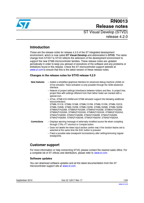
RN0013Release notesST Visual Develop (STVD)release 4.2.0IntroductionThese are the release notes for release 4.2.0 of the ST integrated developmentenvironment, which is now called ST Visual Develop and abbreviated to STVD. The namechange from STVD7 to STVD reflects the extension of the development environment tosupport the new STM8 microcontroller families. These release notes are updatedperiodically in order to keep you abreast of evolutions of the software and any problems orlimitations found in this release. Check the ST microcontroller support website at to ensure that this is the latest version of these release notes.Changes in the release notes for STVD release 4.2.0New features–Added a simplified graphical interface for advanced debug machine (ADM) onSTice emulator. Trace activation is only possible through the ADM advancedinterface.–Rework of project settings inheritance between folders and files. In project tree,project files with settings different from their father folder are marked with aspecial icon.–STice, STM8-ICD-SWIM and STM8 simulator support the following additionalmicrocontrollers:STM8L151C8, STM8L151M8, STM8L151R8, STM8L151R6, STM8L152C8,STM8L152M8, STM8L152R8, STM8L152R6, STM8L162M8, STM8L162R8.STM8A(F/H)5268, STM8A(F/H)5269, STM8A(F/H)5288, STM8A(F/H)5289,STM8A(F/H)528A, STM8A(F/H)52A8, STM8A(F/H)52A9, STM8A(F/H)52AA,STMA(F/H)6269, STMA(F/H)6286, STMA(F/H)6288, STMA(F/H)6289,STMA(F/H)628A, STMA(F/H)62A8, STMA(F/H)62A9, STMA(F/H)62AA.Corrections–Displays warning message of externally modified source file when compilingthrough CTRL+F7 shortcut or Compile button.–Does not delete the linker input section (entire row) if the Section Name cell isselected at the same time the ESC button is pressed.–Fixed a possible data breakpoint inconsistency after setting/removing regularbreakpoints.Customer supportFor more information or help concerning STVD, please contact the nearest sales office. Fora complete list of ST offices and distributors, please refer to .Software updatesY ou can download software updates and all the latest documentation from the STmicrocontroller support site at .September 2010Doc ID 12917 Rev 171/29Contents RN0013Contents1Read me first . . . . . . . . . . . . . . . . . . . . . . . . . . . . . . . . . . . . . . . . . . . . . . . 41.1Host PC system requirements . . . . . . . . . . . . . . . . . . . . . . . . . . . . . . . . . . 41.2Emulation hardware support . . . . . . . . . . . . . . . . . . . . . . . . . . . . . . . . . . . 41.3About using the Cosmic C toolset . . . . . . . . . . . . . . . . . . . . . . . . . . . . . . . 41.4About using the Metrowerks C toolset . . . . . . . . . . . . . . . . . . . . . . . . . . . . 41.5About using the Raisonance C toolset . . . . . . . . . . . . . . . . . . . . . . . . . . . . 52What’s new in STVD release 4.2.0? . . . . . . . . . . . . . . . . . . . . . . . . . . . . . 52.1Summary of changes in release 4.2.0 . . . . . . . . . . . . . . . . . . . . . . . . . . . . 52.2Hardware and targets supported by this release . . . . . . . . . . . . . . . . . . . . 52.2.1STice advanced emulation system . . . . . . . . . . . . . . . . . . . . . . . . . . . . . 62.2.2STM8-ICD-SWIM . . . . . . . . . . . . . . . . . . . . . . . . . . . . . . . . . . . . . . . . . . . 72.2.3ST7-EMU3 emulators . . . . . . . . . . . . . . . . . . . . . . . . . . . . . . . . . . . . . . . 82.2.4ST7-DVP3 emulators . . . . . . . . . . . . . . . . . . . . . . . . . . . . . . . . . . . . . . . . 82.2.5ST7-ICD-ICC . . . . . . . . . . . . . . . . . . . . . . . . . . . . . . . . . . . . . . . . . . . . . . 92.2.6ST7-EMU2 (HDS2) emulators . . . . . . . . . . . . . . . . . . . . . . . . . . . . . . . . . 92.2.7ST7-DVP/DVP2 emulators (first and second generation) . . . . . . . . . . . 102.2.8Simulators . . . . . . . . . . . . . . . . . . . . . . . . . . . . . . . . . . . . . . . . . . . . . . . 103Known problems/limitations . . . . . . . . . . . . . . . . . . . . . . . . . . . . . . . . . 123.1Known problems/limitations for STVD installer . . . . . . . . . . . . . . . . . . . . . 123.2Known problems/limitations for STVD interface . . . . . . . . . . . . . . . . . . . . 123.2.1Cosmic C toolset . . . . . . . . . . . . . . . . . . . . . . . . . . . . . . . . . . . . . . . . . . 123.2.2Metrowerks C toolset . . . . . . . . . . . . . . . . . . . . . . . . . . . . . . . . . . . . . . . 123.3Known problems/limitations for debug interface . . . . . . . . . . . . . . . . . . . . 123.4Known problems/limitations for STice targets . . . . . . . . . . . . . . . . . . . . . 133.4.1Trace . . . . . . . . . . . . . . . . . . . . . . . . . . . . . . . . . . . . . . . . . . . . . . . . . . . 133.4.2NEM breakpoints . . . . . . . . . . . . . . . . . . . . . . . . . . . . . . . . . . . . . . . . . . 133.4.3Profiler . . . . . . . . . . . . . . . . . . . . . . . . . . . . . . . . . . . . . . . . . . . . . . . . . . 133.4.4USB . . . . . . . . . . . . . . . . . . . . . . . . . . . . . . . . . . . . . . . . . . . . . . . . . . . . 143.5Known problems for STM8-ICD-SWIM targets . . . . . . . . . . . . . . . . . . . . . 143.6Known problems/limitations for ST7-EMU3 targets . . . . . . . . . . . . . . . . . 143.6.1ST7MDT10-EMU3 . . . . . . . . . . . . . . . . . . . . . . . . . . . . . . . . . . . . . . . . . 15 2/29 Doc ID 12917 Rev 17RN0013Contents3.7Known problems/limitations for ST7-DVP3 targets . . . . . . . . . . . . . . . . . . 153.7.1ST7MDT10-DVP3 . . . . . . . . . . . . . . . . . . . . . . . . . . . . . . . . . . . . . . . . . 153.8Known problems/limitations for ST7-ICD targets . . . . . . . . . . . . . . . . . . . 163.9Known problems/limitations for ST7-EMU2 (HDS2) targets . . . . . . . . . . . 163.9.1ST7263x-EMU2 emulator . . . . . . . . . . . . . . . . . . . . . . . . . . . . . . . . . . . 163.9.2ST7MDTU5-EMU2B emulator . . . . . . . . . . . . . . . . . . . . . . . . . . . . . . . . 173.10Known problems/limitations for ST7-DVP/DVP2 targets . . . . . . . . . . . . . 173.11Known problems/limitations for simulators . . . . . . . . . . . . . . . . . . . . . . . . 174Information for major previous releases . . . . . . . . . . . . . . . . . . . . . . . . 184.1Summary of changes in release 4.1.6 . . . . . . . . . . . . . . . . . . . . . . . . . . . 184.2Summary of changes in release 4.1.5 . . . . . . . . . . . . . . . . . . . . . . . . . . . 184.3Summary of changes in release 4.1.4 . . . . . . . . . . . . . . . . . . . . . . . . . . . 184.4Summary of changes in release 4.1.3 . . . . . . . . . . . . . . . . . . . . . . . . . . . 194.5Summary of changes in release 4.1.2 . . . . . . . . . . . . . . . . . . . . . . . . . . . 194.6Summary of changes in release 4.1.1 . . . . . . . . . . . . . . . . . . . . . . . . . . . 204.7Summary of changes in release 4.1.0 . . . . . . . . . . . . . . . . . . . . . . . . . . . 204.8Summary of changes in release 4.0.1 . . . . . . . . . . . . . . . . . . . . . . . . . . . 214.9Summary of changes in release 4.0 . . . . . . . . . . . . . . . . . . . . . . . . . . . . . 224.10Summary of changes in release 3.5.0 . . . . . . . . . . . . . . . . . . . . . . . . . . . 234.11Summary of changes in release 3.4.0 . . . . . . . . . . . . . . . . . . . . . . . . . . . 244.12Summary of changes in release 3.3.4 (April 2007) . . . . . . . . . . . . . . . . . 254.13Summary of changes in release 3.3.3 (December 2006) . . . . . . . . . . . . . 26 5Revision history . . . . . . . . . . . . . . . . . . . . . . . . . . . . . . . . . . . . . . . . . . . 27Doc ID 12917 Rev 173/29Read me first RN00134/29 Doc ID 12917 Rev 171 Read me firstThis section provides important information about STVD release 4.2.0.1.1Host PC system requirements PC and compatibles running with Windows XP , and Vista ® 32-bit operating systems.Note:1Administrator privileges are required to install STVD and to connect emulators to the USB port for the first time. Power user or administrator privileges are required to run STVD.2Under the Vista operating system, you must run STVD as administrator. Y ou can either turnoff the User Account Control feature (not recommended), or use the Run as Administratorcommand from the contextual menu, then Allow execution.1.2 Emulation hardware supportThis version includes the ST7 simulator (no emulation hardware required) and supportscertain ST7-EMU2 (HDS2) emulators with active probes, all generations of ST7-DVPxemulators, ST7-EMU3 series emulators and in-circuit debugging with the ST7-EMU3 withICC Add-on, the ST7-DVP3 series emulators, the Raisonance RLink, ST7-STICK, ST -LINK,and the STice advanced emulation system.Listings of supported ST7 and STM8 devices for each STVD debugging target (emulators,ICD and Simulator) are provided in Section 2.2 on page 5.1.3 About using the Cosmic C toolsetSTVD release 4.2.0 was validated using the Cosmic C toolset versions 4.5.7 for ST7, and4.3.3 for STM8. In order to use the Cosmic C toolset with STVD, the cvdwarf.exe Cosmicconvertor is needed to generate the .elf debug information files required by STVD. Thecvdwarf.exe Cosmic converter is included in the Cosmic C toolset versions 4.2a and later.Y ou can download this or a later version from: .1.4About using the Metrowerks C toolset STVD is no longer validated with Metrowerks C toolset.Note:1The industry standard ELF/Dwarf format is the default output format for the Metrowerks Ctoolset. When building, the -f2 option for the C compiler and the lib.e20 library arechosen by default.2For reasons of legacy compatibility, the Metrowerks C toolset and STVD continue to supportthe proprietary Hiware format. However, Hiware format users must use a script link file in theProject Settings interface when building their applications.3Any references to “Metrowerks” and “Hiware” in STVD software, examples anddocumentation refer to the Metrowerks C toolset.1.5 About using the Raisonance C toolsetSTVD release 4.2.0 was validated using version 2.28 of the Raisonance C toolset. In orderto use the Raisonance C toolset with STVD, the omf2elf.exe Raisonance convertor isneeded to generate the .elf debug information files required by STVD. The omf2elf.exeRaisonance converter is included in the Raisonance C toolset.2 What’s new in STVD release 4.2.0?2.1 Summary of changes in release 4.2.0New features●Added a simplified graphical interface for advanced debug machine (ADM) on STiceemulator. Trace activation is only possible through the ADM advanced interface, notthrough the simplified one.●Rework of project settings inheritance between folders and files. In project tree, projectfiles with settings different from their father folder are marked with a special icon.●STice, STM8-ICD-SWIM and STM8 simulator support the following additionalmicrocontrollers:–STM8L151C8, STM8L151M8, STM8L151R8, STM8L151R6, STM8L152C8,STM8L152M8, STM8L152R8, STM8L152R6, STM8L162M8, STM8L162R8.–STM8A(F/H)5268, STM8A(F/H)5269, STM8A(F/H)5288, STM8A(F/H)5289,STM8A(F/H)528A, STM8A(F/H)52A8, STM8A(F/H)52A9, STM8A(F/H)52AA,STMA(F/H)6269, STMA(F/H)6286, STMA(F/H)6288, STMA(F/H)6289,STMA(F/H)628A, STMA(F/H)62A8, STMA(F/H)62A9, STMA(F/H)62AA.Corrections●Displays warning message of externally modified source file when compiling throughCTRL+F7 shortcut or Compile button.●Does not delete the linker input section (entire row) if the Section Name cell is selectedat the same time the ESC button is pressed.●Fixed a possible data breakpoint inconsistency after setting/removing regularbreakpoints.2.2 Hardware and targets supported by this releaseThe ‘F’ notation in MCU names denoting ‘Flash’ variants is only indicated for ICD. Debuginstruments support emulation/simulation of Flash variants of the listed MCUs, unlessotherwise indicated.Doc ID 12917 Rev 175/292.2.1 STice advanced emulation systemList of supported devices for emulation with STice:STM8A(F/H)5168, STM8A(F/H)5169, STM8A(F/H)5178, STM8A(F/H)5179, STM8A(F/H)5188,STM8A(F/H)5189, STM8A(F/H)518A, STM8A(F/H)5198, STM8A(F/H)5199, STM8A(F/H)519A,STM8A(F/H)51A8, STM8A(F/H)51A9, STM8A(F/H)51AASTM8A(F/H)5268, STM8A(F/H)5269, STM8A(F/H)5288, STM8A(F/H)5289, STM8A(F/H)528A,STM8A(F/H)52A8, STM8A(F/H)52A9, STM8A(F/H)52AASTM8A(F/H)6126, STM8A(F/H)6146, STM8A(F/H)6148, STM8A(F/H)6166, STM8A(F/H)6168,STM8A(F/H)6169, STM8A(F/H)6176, STM8A(F/H)6178, STM8A(F/H)6179, STM8A(F/H)6186,STM8A(F/H)6188, STM8A(F/H)6189, STM8A(F/H)618A, STM8A(F/H)6198, STM8A(F/H)6199,STM8A(F/H)619A, STM8A(F/H)61A8, STM8A(F/H)61A9, STM8A(F/H)61AASTMA(F/H)6269, STMA(F/H)6286, STMA(F/H)6288, STMA(F/H)6289, STMA(F/H)628A,STMA(F/H)62A8, STMA(F/H)62A9, STMA(F/H)62AASTM8AF6226, STM8AF6246, STM8AF6248, STM8AF6266, STM8AF6268STM8L101F2(P/U), STM8L101F3(P/U), STM8L101G2U, STM8L101G3U, STM8L101K3USTM8L151C(4/6), STM8L151C8, STM8L151G(4/6), STM8L151K(4/6), STM8L151M8, STM8L151R6,STM8L151R8STM8L152C(4/6), STM8L152C8, STM8L152K(4/6), STM8L152M8, STM8L152R6, STM8L152R8STM8L162M8, STM8L162R8STM8S103F2(P/U), STM8S103F3(P/U), STM8S103K3USTM8S105C4, STM8S105C6, STM8S105K4, STM8S105K6, STM8S105S4, STM8S105S6STM8S207CB, STM8S207MB, STM8S207RB, STM8S207SB, STM8S207C6, STM8S207K6,STM8S207R6, STM8S207S6, STM8S207C8, STM8S207M8, STM8S207R8, STM8S207S8STM8S208C6, STM8S208R6, STM8S208S6, STM8S208C8, STM8S208R8, STM8S208S8,STM8S208CB, STM8S208MB, STM8S208RB, STM8S208SBSTM8S903K3, STM8S903F36/29 Doc ID 12917 Rev 172.2.2 STM8-ICD-SWIMList of supported devices for in-circuit debugging from STVD with ST-Link, RLink, or STice:STM8A(F/H)5168, STM8A(F/H)5169, STM8A(F/H)5178, STM8A(F/H)5179, STM8A(F/H)5188,STM8A(F/H)5189, STM8A(F/H)518A, STM8A(F/H)5198, STM8A(F/H)5199, STM8A(F/H)519A,STM8A(F/H)51A8, STM8A(F/H)51A9, STM8A(F/H)51AASTM8A(F/H)5268, STM8A(F/H)5269, STM8A(F/H)5288, STM8A(F/H)5289, STM8A(F/H)528A,STM8A(F/H)52A8, STM8A(F/H)52A9, STM8A(F/H)52AASTM8A(F/H)6126, STM8A(F/H)6146, STM8A(F/H)6148, STM8A(F/H)6166, STM8A(F/H)6168,STM8A(F/H)6169, STM8A(F/H)6176, STM8A(F/H)6178, STM8A(F/H)6179, STM8A(F/H)6186,STM8A(F/H)6188, STM8A(F/H)6189, STM8A(F/H)618A, STM8A(F/H)6198, STM8A(F/H)6199,STM8A(F/H)619A, STM8A(F/H)61A8, STM8A(F/H)61A9, STM8A(F/H)61AASTMA(F/H)6269, STMA(F/H)6286, STMA(F/H)6288, STMA(F/H)6289, STMA(F/H)628A,STMA(F/H)62A8, STMA(F/H)62A9, STMA(F/H)62AASTM8AF6226, STM8AF6246, STM8AF6248, STM8AF6266, STM8AF6268STM8L101F2(P/U), STM8L101F3(P/U), STM8L101G2U, STM8L101G3U, STM8L101K3(U/T)STM8L151C(4/6), STM8L151C8, STM8L151G(4/6), STM8L151K(4/6), STM8L151M8, STM8L151R6,STM8L151R8STM8L152C(4/6), STM8L152C8, STM8L152K(4/6), STM8L152M8, STM8L152R6, STM8L152R8STM8L162M8, STM8L162R8STM8S103F2(P/U), STM8S103F3(P/U), STM8S103K3USTM8S105C4, STM8S105C6, STM8S105K4, STM8S105K6, STM8S105S4, STM8S105S6STM8S207CB, STM8S207MB, STM8S207RB, STM8S207SB, STM8S207K6, STM8S207R6,STM8S207C8, STM8S207M8, STM8S207R8, STM8S207S8STM8S208C6, STM8S208R6, STM8S208S6, STM8S208C8, STM8S208R8, STM8S208S8,STM8S208CB, STM8S208MB, STM8S208RB, STM8S208SBSTM8S903K3, STM8S903F3Doc ID 12917 Rev 177/298/29 Doc ID 12917 Rev 172.2.3 ST7-EMU3 emulatorsList of supported devices by emulator:2.2.4 ST7-DVP3 emulatorsList of supported devices by emulator:ST7MDT10-EMU3ST72260G1, ST72262G(1/2), ST72264G(1/2), ST7DALI, ST7LCD1,ST7LIT10BF(0/1), ST7LIT15BF(0/1), ST7LIT19BF(0/1), ST7LIT10BY(0/1),ST7LIT15BY(0/1), ST7LIT19BY(0/1), ST7LITE(02/05/09/10/15/19/20/25/29/30/35/39), ST7LITES(2/5), ST7LITEUS(2/5), ST7FLITEU0(2/5/9),ST7L(05/09/15/19/34/35/38/39)ST7MDT20J-EMU3ST72321BJ(6/7/9), ST72321J(7/9), ST72321BK6,ST72324BJ(2/4/6), ST72324BK(2/4/6), ST72324BLJ(2/4/6), ST72324BLK(2/4/6),ST72324J(2/4/6), ST72324K(2/4/6), ST72324LJ(2/4/6), ST72324LK(4/6),ST72325C(4/6), ST72325J(4/6/7/9), ST72325K(4/6),ST7232AJ(1/2), ST7232AK(1/2)ST7MDT20M-EMU3ST72321AR(6/7/9), ST72321BAR(6/7/9), ST72321BR(6/7/9), ST72321R(6/7/9),ST72325AR(6/7/9), ST72325R(6/7/9),ST72521AR(6/9), ST72521BAR(6/9), ST72521BR(6/9), ST72521BM9,ST72521M9, ST72521R(6/9)ST7MDT50-EMU3ST7MC1K(2/4/6), ST7MC2(N6/M9/R6/R7/S4/S6), ST7MC2(S7/R9/S9)ST7MDT40-EMU3(ST7MIDI-EMU3)ST72340K(2/4), ST72340S(2/4), ST72344K(2/4), ST72344JS2/4), ST72345C4ST7DVD3-EMU3DVD3, L6315_10_RAM, L6315_10_ROMST7MDTH1-EMU3ST7XGAM(J4T1/K4M1), ST7XGAM(J6T1/K6M1), ST7HUBAR4T1,ST7HUBAR6T1ST7MDTU3-EMU3ST7260E(1/2), ST7260K(1/2),ST7263BE(1/2/4/6), ST7263BH(2/6),ST7263BK(1/2/4/6)ST7MDTU7-EMU3ST7267ST7FLCD-EMU3ST7LCD1ST7MDT10-DVP3ST72260G1, ST72262(G1/G2), ST72264(G1/G2), ST7DALI,ST7LIT10BF(0/1), ST7LIT15BF(0/1), ST7LIT19BF(0/1), ST7LIT10BY(0/1),ST7LIT15BY(0/1), ST7LIT19BY(0/1), ST7LITE(02/05/09/10/15/19/20/25/29/30/35/39), ST7LITES(2/5), ST7LITEUS(2/5), ST7L(05/09/15/19/34/35/38/39)ST7MDT20-DVP3ST72321AR(6/7/9), ST72321BAR(6/7/9), ST72321BJ(6/7/9), ST72321BK6,ST72321BR(6/7/9), ST72321J(7/9), ST72321M(6/9), ST72321R(6/7/9),ST72324BJ(2/4/6), ST72324BK(2/4/6), ST72324BLJ(2/4), ST72324BLK(2/4),ST72324J(2/4/6), ST72324K(2/4/6), ST72324LJ(2/4/6), ST72324LK(2/4/6),ST72325AR(6/7/9), ST72325C(4/6), ST72325J(4/6/7/9), ST72325K(4/6),ST72325R(6/7/9)ST72521AR(6/9), ST72521BAR(6/9), ST72521BM9, ST72521BR(6/9),ST72521M9, ST72521R(6/9),ST7232AJ(1/2), ST7232AK(1/2)ST7MDT25-DVP3ST72361AR(4/6/7/9), ST72361J(4/6/7/9), ST72361K(4/6/7/9),ST72361R(4/6/7/9),ST72561AR(4/6/7/9), ST72561J(4/6/7/9), ST72561K(4/6/7/9), ST72561R(4/6/7/9)Doc ID 12917 Rev 179/292.2.5 ST7-ICD-ICCApplications can be in-circuit debugged on the microcontrollers listed below from STVDusing any of the following development tools:●ST7MDT10-DVP3, ST7MDT20-DVP3, ST7MDT25-DVP3 series emulators: they are all are accessed from STVD as ICD (ST Micro Connect or DVP3).●ST7-EMU3 series emulators – ST Micro Connect with ICC add-on. They are all are accessed from STVD as ICD (ST Micro Connect or DVP3).●RLink from Raisonance (accessed from STVD as ICD RLink ).●ST7-STICK (accessed from STVD as ICD Stick ).List of supported devices for in-circuit debugging.2.2.6 ST7-EMU2 (HDS2) emulatorsList of supported devices by emulator:ST72260G1, ST72262(G1/G2), ST72264(G1/G2), ST7267ST7FDALI, ST7FLCD1ST7FLIT10BF(0/1), ST7FLIT15BF(0/1), ST7FLIT19BF(0/1), ST7FLIT10BY(0/1), ST7FLIT15BY(0/1),ST7FLIT19BY(0/1)ST7FLITE0(2/5/9), ST7FLITE1(0/5/9), ST7FLITE2(0/5/9), ST7FLITE3(0/5/9), ST7FLITES(2/5),ST7FLITEUS(2/5), ST7FLITEUSICD, ST7FLITEU0ICDST7FL1(5/9), ST7FL3(4/5/8/9)ST7WIND11, ST7WIND21ST7FMC1K(2/4/6), ST7FMC2(M9/N6/R6/R7/R9/S4/S6/S7/S9), ST7FMC2R9, ST7FMC2S9ST72F321BAR(6/7/9), ST72F321BJ(6/7/9), ST72F321BK6, ST72F321BR(6/7/9),ST72F325AR(6/7/9), ST72F325C(4/6), ST72F325J(4/6/7/9), ST72F325K(4/6), ST72F325R(6/7/9),ST72F325S(4/6),ST72F340(K2/K4/S2/S4), ST72F344(K2/K4/S2/S4),ST72F345C4ST7FLITE49MST7FOXK1, ST7FOXK2, ST7FOXF1, ST7FLITE49K2T6, ST7FLITE49K2B6ST7MDT00-EMU2B ST7LITE0(5/9)ST7MDT1-EMU2B ST72104G(1/2), ST72215G2, ST72216G1, ST72254G(1/2)ST7MDT2-EMU2A ST72124J2, ST72311R(6/7/9)ST7MDT2-EMU2B ST72314J(2/4), ST72314N(2/4), ST72334J(2/4), ST72334N(2/4),ST72511R(6/7/9) ST72512R4, ST72532R4ST7MDT5-EMU2B ST72141ST7MDT6-EMU2B ST72171K2(B/M)6ST7MDT7-EMU2B ST72C411R1ST7MDTS1-EMU2B ST7SCR1(E/R)ST7MDTU2-EMU2B ST72611F1, ST72P611F4, ST72621J(2/4), ST72621K4, ST72621L4,ST72622(K/L)2, ST72623F2ST7MDTU3-EMU2B ST7263BK(1/2), ST7263BK4ST7MDTU5-EMU2B ST72651, ST72652ST7263-EMU2BST72631, ST72632, ST72633ST72774-EMU2B ST72734J6, ST72754J(6/9), ST72774J(6/7/9)(continued)10/29 Doc ID 12917 Rev 172.2.7 ST7-DVP/DVP2 emulators (first and second generation)2.2.8 Simulators(ST7-EMU2 (HDS2) emulators continued)ST7MDT1-EMU2ST72101G(1/2), ST72212G2, ST72213G1, ST72251G(1/2)ST7255B-EMU2ST7255B ST7285-EMU2ST7285ST7291-EMU2ST7291L(2/3/4/5/5A/6)ST72589B-EMU2ST72389(B/C), ST72589(B/C)ST7MDT1-DVPST72101G(1/2), ST72212G2, ST72213G1, ST72251G(1/2)ST7MDT1-DVP2ST72101G(1/2), ST72104G(1/2), ST72212G2, ST72213G1, ST72215G2, ST72216G1, ST72251G(1/2), ST72254G(1/2)ST7MDT2-DVPST72121J(2/4), ST72311J(2/4), ST72311N(2/4), ST72331J(2/4), ST72331N(2/4)ST7MDT2-DVP2ST72124J2, ST72311R(6/7/9), ST72314J(2/4), ST72314N(2/4), ST72334J(2/4), ST72334N(2/4), ST72511R(6/7/9), ST72512R4, ST72532R4ST7MDP-DVP2ST7MDPST7 baseline ST72101G(1/2), ST72104G(1/2), ST72121J(2/4), ST72124J2, ST72212G2,ST72213G1, ST72215G2, ST72216G1, ST72251G(1/2), ST72254G(1/2),ST72311J(2/4), ST72311N(2/4), ST72311R(6/7/9), ST72314J(2/4),ST72314N(2/4), ST72331J(2/4), ST72331N(2/4), ST72334J(2/4),ST72334N(2/4)ST7 lite ST72260G1, ST72262G(1/2), ST72264G(1/2), ST7DALI, ST7LIT10BF(0/1),ST7LIT15BF(0/1), ST7LIT19BF(0/1), ST7LIT10BY(0/1), ST7LIT15BY(0/1),ST7LIT19BY(0/1), ST7LITE(02/05/09/10/15/19/20/25/29/30/35/39),ST7LITES(2/5), ST7L(05/09/35/39), ST7FLITEU0(2/5/9), ST7FLITE49M,ST7FOXK1, ST7FOXK2, ST7FOXF1, ST7FOXA0, ST7FLUS5, ST7FLU05,ST7FLU09, ST7FLI49K2T6, ST7FLI49K2B6ST7 mid-range ST7232AJ(1/2), ST7232AK(1/2), ST72321AR(6/9), ST72321BAR(6/7/9),ST72321BJ(6/7/9), ST72321BK6, ST72321BR(6/7/9), ST72321J(7/9),ST72321M(6/9), ST72321BM(6/9), ST72321R(6/7/9), ST72324BJ(2/4/6),ST72324BK(2/4/6), ST72324BLJ(2/4), ST72324BLK(2/4), ST72324J(2/4/6),ST72324K(2/4/6), ST72324LS(2/4), ST72324BLS(2/4), ST72325AR(6/7/9),ST72325C(6/7/9), ST72325S(6/7/9), ST72325J(4/6/7/9), ST72325K(4/6),ST72325R(7/9), ST72361AR(4/6/7/9), ST72361J(4/6/7/9), ST72361K(4/6/7/9),ST72361R(4/6/7/9), ST72340K(2/4), ST72340S(2/4), ST72344K(2/4),ST72344S(2/4), ST72345C4ST7 CAN ST72511R(6/7/9), ST72521AR(6/9), ST72521M9, ST72521R(6/9)ST7 LCD ST72389B, ST72589BST7 MC ST72141ST7 OPST72171(continued)RN0013What’s new in STVD release 4.2.0?(Simulators continued)ST7 USB ST7260E(1/2), ST7260K(1/2), ST72631, ST72632, ST72633, ST7263BD6,ST7263BH(2/6), ST7263BE(1/2/4/6), ST7263BK(1/2/2U1/4/6)STM8STM8A(F/H)5168, STM8A(F/H)5169, STM8A(F/H)5178, STM8A(F/H)5179,STM8A(F/H)5188, STM8A(F/H)5189, STM8A(F/H)518A, STM8A(F/H)5198,STM8A(F/H)5199, STM8A(F/H)519A, STM8A(F/H)51A8, STM8A(F/H)51A9,STM8A(F/H)51AASTM8A(F/H)5268, STM8A(F/H)5269, STM8A(F/H)5288, STM8A(F/H)5289,STM8A(F/H)528A, STM8A(F/H)52A8, STM8A(F/H)52A9, STM8A(F/H)52AASTM8A(F/H)6126, STM8A(F/H)6146, STM8A(F/H)6148, STM8A(F/H)6166,STM8A(F/H)6168, STM8A(F/H)6169, STM8A(F/H)6176, STM8A(F/H)6178,STM8A(F/H)6179, STM8A(F/H)6186, STM8A(F/H)6188, STM8A(F/H)6189,STM8A(F/H)618A, STM8A(F/H)6198, STM8A(F/H)6199, STM8A(F/H)619A,STM8A(F/H)61A8, STM8A(F/H)61A9, STM8A(F/H)61AASTMA(F/H)6269, STMA(F/H)6286, STMA(F/H)6288, STMA(F/H)6289,STMA(F/H)628A, STMA(F/H)62A8, STMA(F/H)62A9, STMA(F/H)62AASTM8AF6226, STM8AF6246, STM8AF6248, STM8AF6266, STM8AF6268STM8L101F2(P/U), STM8L101F3(P/U), STM8L101G2U, STM8L101G3U,STM8L101K3(U/T)STM8S103F2(P/U)STM8S103F3(P/U), STM8S103K3U, STM8S105C4,STM8S105C6, STM8S105K4, STM8S105K6, STM8S105S4, STM8S105S6STM8L151C(4/6), STM8L151C8, STM8L151G(4/6), STM8L151K(4/6),STM8L151M8, STM8L151R6, STM8L151R8STM8L152C(4/6), STM8L152C8, STM8L152K(4/6), STM8L152M8,STM8L152R8, STM8L152R6STM8L162M8, STM8L162R8STM8S207MB, STM8S207RB, STM8S207CB, STM8S207R8, STM8S207C6,STM8S207C8, STM8S207S8, STM8S207S6, STM8S207R6, STM8S207K6,STM8S207M8, STM8S207SB,STM8S208R6, STM8S208C6, STM8S208S6, STM8S208R8, STM8S208C8,STM8S208S8, STM8S208CB, STM8S208SB, STM8S208MB, STM8S208RBSTM8S903K3, STM8S903F3Doc ID 12917 Rev 1711/2912/29 Doc ID 12917 Rev 173 K nown problems/limitations3.1 K nown problems/limitations for STVD installer●Y ou must install STVD prior to connecting a debug instrument to the host PC's USB port, in order to have the necessary driver.●The USB driver for the Raisonance RLink is not installed upon installation of STVD. After installing STVD, RLink users must install the RLink USB driver by selectingStart>ST7 Toolset>Setup>Install RLink driver .3.2 Known problems/limitations for STVD interfaceThe include files provided upon installation of STVD are not the same as those requiredwhen using the ST7 Library or STM8 Library. ST7 and STM8 library users should refer tothe appropriate ST7 or STM8 library documentation for information about the correct includefiles to use.3.2.1 Cosmic C toolsetIn the Cosmic Linker for STM8 microcontrollers, the .const segment must be located in thefirst 64Kbyte segment. This is mandatory because the Cosmic toolset cannot link aninterrupt handler that is not located in segment 1.3.2.2 Metrowerks C toolsetNote:STVD is no longer validated with Metrowerks C toolset.●The automatic generation of the linker PRM file can only be used when generating an executable in ELF/DWARF 2.0 format. For Hiware format, users must use a writtenPRM file.●Using the -StatF= option with Hiware format may cause a failure during linking. The executable is not produced.●When using the recommended ELF format and STVD include files, a link error L1818 may be generated due to paginated registers. Y ou can add the option -wmsgsi1818as a user-defined option. This option converts the error to a warning message only.3.3 K nown problems/limitations for debug interface●When the program is stopped on a breakpoint set on a function name, the displayed argument values may be false.●When .hex or .s19 files are loaded outside of any workspace, an error message is displayed, but it is meaningless.●Double type” variables are referred as “float type” variables.●The const variable qualifier is not displayed.●Only one instance of STVD can run on your PC at any given time.●Reduced user access rights to the database registry or to the STVD install directory can impede the normal use of STVD. A warning message occurs if a read/write accessproblem occurs.3.4 Known problems/limitations for STice targets3.4.1 TraceTrace activation is only possible through the advanced debug machine (ADM) interface onSTice emulator, not through the simplified one.breakpoints3.4.2 NEMNEM breakpoints on data access are limited to the memory area range [0-0x7FFF], NEMbreakpoints on opcode fetch are limited to addresses higher than 0x7FFF.3.4.3 Profiler●Coverage and profiling functionality is limited to core running at up to 24MHz.●Code occurrence and time profiling limitations:–Whatever the time profiling mode, the profiler does not profile the first or the first two instructions after a breakpoint.–It also does not profile correctly the last or the last two instructions before abreakpoint.–The number of occurrences of an interrupted instruction may be false. Inparticular:The occurrence number of the WFE instruction is doubled.The occurrence number of an IRET instruction may be null if it is always executedin a shortened way. A shortened IRET is an IRET which is executed in one cycleonly because of a pending interrupt being serviced immediately after.In some rare cases, the occurrence number of an interrupted instruction isdoubled.●Contrarily to what is said in the online help, the Subroutine mode (interrupt timeexcluded) is not available in this release. Only the Subroutine and Interrupt mode(interrupt time included) is available.●Time profiling limitations in Instruction mode:Context saving time is added to the interrupted instruction time.●Time profiling limitations in the Subroutine and Interrupt mode:–The time for recursive functions is not correct.–The longjmp C library routine should not be used otherwise the results will beerroneous.–The results may be incorrect with the Raisonance compiler if it calls a libraryroutine which uses the stack in a nonstandard way.–For code written in assembly language, the subroutine modes work only if routines use the stack in a standard way. T o be certain there is no problem, make sure thateach routine is called by a call instruction and that it returns to its caller by a returninstruction.–In the case of pending interrupts resulting in the occurrence of several immediately consecutive interrupts, the time of the interrupted instruction doesn't include all thetime spent in the interrupts.–Similarly an IRET followed immediately by a pending interrupt is seen asinterrupted and its time includes the time of the following interrupt.Doc ID 12917 Rev 1713/29。

![[讲稿]ST产品型号命名规则](https://img.taocdn.com/s1/m/040690c13086bceb19e8b8f67c1cfad6195fe98b.png)
ST产品型号命名规则普通线性、逻辑器件MXXX XXXXX XX X X1 2 3 4 51.产品系列:74AC/A CT……先进CMOS HCF4XXXM74HC………高速CMOS2. 序列号3.速度4.封装:BIR,BEY……陶瓷双列直插M,MIR………塑料微型封装5.温度普通存贮器件XX X XXXX X XX X XX1 2 3 4 5 6 7 1.系列:ET21 静态RAMETL21 静态RAMETC27 EPROMMK41 快静态RAMMK45 双极端口FIFOMK48 静态RAMTS27 EPROMS28 EEPROMTS29 EEPROM2.技术:空白…NMOSC…CMOSL…小功率3.序列号4.封装:C 陶瓷双列J 陶瓷双列N 塑料双列Q UV 窗口陶瓷熔封双列直插5.速度6.温度:空白0℃~70℃E -25℃~70℃V -40℃~85℃M -55℃~125℃7.质量等级:空白标准B/B MIL-STD-883B B 级存储器编号(U.V EPROM 和一次可编程OTP)M XX X XXX X X XXX X X1 2 3 4 5 6 7 8 1.系列:27…EPROM87…EPROM 锁存2.类型:空白…NMOS,C…CMOS,V…小功率2.容量:64…64K 位(X8)256…256K 位(X8)512…512K 位(X8)1001…1M 位(X8)101…1M 位(X8)低电压1024…1M 位(X8)2001…2M 位(X8)201…2M 位(X8)低电压4001…4M 位(X8)401…4M 位(X8)低电压4002…4M 位(X16)801…4M 位(X8)161…16M 位(X8/16)可选择160…16M 位(X8/16)4.改进等级5.电压范围:空白 5V +10%Vcc,X 5V +10%Vcc6.速度:55 55n,60 60ns,70 70ns,80 80ns90 90ns,100/10 100 n120/12 120 ns,150/15 150 ns200/20 200 ns,250/25 250 ns7.封装:F 陶瓷双列直插(窗口)L 无引线芯片载体(窗口)B 塑料双列直插C 塑料有引线芯片载体(标准)M 塑料微型封装N 薄型微型封装K 塑料有引线芯片载体(低电压)8.温度:1 0℃~70℃,6 -40℃~85℃,3 -40℃~125℃快闪EPROM 的编号M XX X A B C X X XXX X X1 2 3 4 5 6 7 8 9 10 1.电源2.类型:F 5V +10%,V 3.3V +0.3V3.容量:1 1M,2 2M,3 3M,8 8M,16 16M4.擦除:0 大容量1 顶部启动逻辑块2 底部启动逻辑块 4 扇区5.结构:0 ×8/×16 可选择,1 仅×8,2 仅×166.改型:空白 A7. Vcc:空白 5V+10%VccX +5%Vcc8.速度:60 60ns,70 70ns,80 80ns,90 90ns100 100ns,120 120ns,150 150ns,200 200ns9.封装:M 塑料微型封装N 薄型微型封装,双列直插C/K 塑料有引线芯片载体B/P 塑料双列直插10.温度:1 0℃~70℃,6 -40℃~85℃,3 -40℃~125℃仅为3V 和仅为5V 的快闪EPROM 编号M XX X XXX X XXX X X1 2 3 4 5 6 7 1.器件系列:29 快闪2.类型:F 5V 单电源V 3.3 单电源3.容量:100T (128K×8.64K×16)顶部块,100B (128K×8.64K×16)底部块200T (256K×8.64K×16)顶部块,200B (256K×8.64K×16)底部块400T (512K×8.64K×16)顶部块,400B (512K×8.64K×16)底部块040 (12K×8)扇区,080 (1M×8)扇区016 (2M×8)扇区4.Vcc:空白 5V+10%Vcc,X +5%Vcc5.速度:60 60ns,70 70ns,80 80ns90 90ns,120 120ns6.封装:M 塑料微型封装N 薄型微型封装K 塑料有引线芯片载体P 塑料双列直插7.温度:1 0℃~70℃,6 -40℃~85℃,3 -40℃~125℃串行EEPROM 的编号ST XX XX XX X X X1 2 3 4 5 6 1.器件系列:24 12C ,25 12C(低电压),93 微导线95 SPI 总线28 EEPROM2.类型/工艺:C CMOS(EEPROM)E 扩展I C 总线W 写保护士CS 写保护(微导线)P SPI 总线LV 低电压(EEPROM)3.容量:01 1K,02 2K,04 4K,08 8K16 16K,32 32K,64 64K4.改型:空白 A、 B、 C、 D 5.封装:B 8 腿塑料双列直插M 8 腿塑料微型封装ML 14 腿塑料微型封装6.温度:1 0℃~70℃6 -40℃~85℃3 -40℃~125℃微控制器编号ST XX X XX X X1 2 3 4 5 6 1.前缀2.系列:62 普通ST6 系列63 专用视频ST6 系列72 ST7 系列90 普通ST9 系列92 专用ST9 系列10 ST10 位系列20 ST20 32 位系列3.版本:空白 ROMT OTP(PROM)R ROMlessP 盖板上有引线孔E EPROMF 快闪4.序列号5.封装:B 塑料双列直插D 陶瓷双列真插F 熔封双列直插M 塑料微型封装S 陶瓷微型封装CJ 塑料有引线芯片载体K 无引线芯片载体L 陶瓷有引线芯片载体QX 塑料四面引线扁平封装G 陶瓷四面扁平封装成针阵列R 陶瓷什阵列T 薄型四面引线扁平封装6.温度范围:1.5 0℃~70℃(民用)2 -40℃~125℃(汽车工业)61 -40℃~85℃(工业)E -55℃~125℃。

由衷地感謝您購買日本サンケン(S A N K E N )牌32位元R I S C 架構、具有V /F 控制模式與Se n s o r l e s s �或稱速度推算式、無速度傳感式�向量控制模式可供選擇的S A M C O -v m 05系列雙重額定、高性能、靜音型汎用變頻器。
裝設這部變頻器之後�您的三相感應馬達立刻具有無段變速的機能。
由於32位元R I S C 演算速度快、程式容量大�因此具備多機能、操作容易的特點。
為了讓您充分地享用這部變頻器的特性與機能�務必詳閱這本操作說明書。
當您使用中發現任何疑難時�請立刻就近向士林電機的F A 產品經銷商洽詢�或撥電話�03�597-0921轉231~233通知士林電機自動化營業部營業三課�我們的專業人員隨時都等待著為您做熱誠地服務。
在此我們再度深切地期望您永遠愛顧 的優良產品。
台灣總代理�士林電機廠股份有限公司安全通告●為了要預先防範您以及第三者因採用本產品而導致對人體危害或財產損失�因此在這本操作說明書上明確地登載著各種警告與禁制事項�請務必遵守。
使用本產品以前請務必詳閱這本操作說明書�並請依照正確的方式使用。
●這本操作說明書務必放置在設備、機台的旁邊或是便於取閱的地方�以便使用者查閱。
●對於安全注意事項等級�在說明書內分為「危險」、「注意」兩級。
操作人員如果不理會而誤操作時�可能會造成人體傷害或對財物造成損失的事項。
注意操作人員如果不理會而誤操作時�可能會對人體造成傷亡事件的事項。
危險※還有�即使是「注意」所記載內容都是屬於必需遵守的重要事項�不予理會時亦可能會引發不可臆測的後果。
標誌之後所敘述的是具體的強制內容。
強制�不可不為�標誌標誌之後所敘述的是具體的禁止內容。
禁止�不可為�標誌標誌之後所敘述的是具體的注意內容。
注意標誌標誌之後所敘述的是具體的危險內容。
危險標誌標誌解說安全注意事項1.請採用3-2-(1)所指定的螺絲�將變頻器牢牢地固定在平整的水泥或金屬板類的牆面上�並加以適當地屏蔽。