CD74ACT573MG4中文资料
- 格式:pdf
- 大小:649.99 KB
- 文档页数:15

MC74AC573, MC74ACT573Octal Buffer/Line Driver with 3−State OutputsThe MC74AC573/74ACT573 is a high−speed octal latch with buffered common Latch Enable (LE) and buffered common Output Enable (OE) inputs.The MC74AC573/74ACT573 is functionally identical to the MC74AC373/74ACT373 but has inputs and outputs on opposite sides.Features•Inputs and Outputs on Opposite Sides of Package Allowing Easy Interface with Microprocessors•Useful as Input or Output Port for Microprocessors •Functionally Identical to MC74AC373/74ACT373•3−State Outputs for Bus Interfacing •Outputs Source/Sink 24 mA•′ACT573 Has TTL Compatible Inputs •Pb−Free Packages are Available*Figure 1. Pinout 20−Lead Packages Conductors(Top View)192018171615142134567V CC 1381291110O 0O 1O 2O 3O 4O 5O 6O 7LE OED 0D 1D 2D 3D 4D 5D 6D 7GNDPIN ASSIGNMENTPIN FUNCTIOND 0−D 7Data Inputs LE Latch Enable InputOE 3−State Output Enable Input O 0−O 73−State Latch OutputsFigure 2. Logic Symbol*For additional information on our Pb−Free strategy and soldering details, please download the ON Semiconductor Soldering and Mounting Techniques Reference Manual, SOLDERRM/D.PDIP−20N SUFFIXCASE 738SO−20DW SUFFIX CASE 751DTSSOP−20DT SUFFIX CASE 948EEIAJ−20M SUFFIX CASE 967See detailed ordering and shipping information in the package dimensions section on page 8 of this data sheet.ORDERING INFORMATIONMC74xxx573N AWLYYWWGxxx 573ALYW GG74xxx573AWLYWWGxxx = AC or ACT A = Assembly Location WL, L = Wafer Lot YY , Y = YearWW, W = Work WeekG or G = Pb−Free Package(Note: Microdot may be in either location)MARKING DIAGRAMTRUTH TABLEInputsOutputs OE LE D n O n L H H H L H L L L L X O 0HXXZH = HIGH Voltage Level L = LOW Voltage Level Z = High Impedance X = ImmaterialO 0 = Previous O 0 before LOW−to−HIGH Transition of ClockFunctional DescriptionThe MC74AC573/74ACT574 contains eight D−type latches with 3−state output buffers. When the Latch Enable (LE) input is HIGH, data on the D n inputs enters the latches.In this condition the latches are transparent, i.e., a latch output will change state each time its D input changes. When LE is LOW the latches store the information that was present on the D inputs a setup time preceding the HIGH−to−LOW transition of LE. The 3−state buffers are controlled by the Output Enable (OE) input. When OE is LOW, the buffers are enabled. When OE is HIGH the buffers are in the high impedance mode but this does not interfere with entering new data into the latches.Figure 3. Logic Diagram1234567NOTE:That this diagram is provided only for the understanding of logic operations and should not be used to estimate propagation delays.MAXIMUM RATINGSSymbol Parameter Value UnitV CC DC Supply Voltage (Referenced to GND)−0.5 to +7.0VV IN DC Input Voltage (Referenced to GND)−0.5 to V CC +0.5VV OUT DC Output Voltage (Referenced to GND)−0.5 to V CC +0.5VI IN DC Input Current, per Pin±20mAI OUT DC Output Sink/Source Current, per Pin±50mAI CC DC V CC or GND Current per Output Pin±50mAT stg Storage Temperature−65 to +150°C Maximum ratings are those values beyond which device damage can occur. Maximum ratings applied to the device are individual stress limit values (not normal operating conditions) and are not valid simultaneously. If these limits are exceeded, device functional operation is not implied, damage may occur and reliability may be affected.RECOMMENDED OPERATING CONDITIONSSymbol Parameter Min Typ Max UnitV CC Supply Voltage ′AC 2.0 5.0 6.0V ′ACT 4.5 5.0 5.5V IN, V OUT DC Input Voltage, Output Voltage (Ref. to GND)0−V CC Vt r, t f Input Rise and Fall Time (Note 1)′AC Devices except Schmitt InputsV CC @ 3.0 V−150−V CC @ 4.5 V−40−ns/VV CC @ 5.5 V−25−t r, t f Input Rise and Fall Time (Note 2)′ACT Devices except Schmitt InputsV CC @ 4.5 V−10−ns/VV CC @ 5.5 V−8.0−T J Junction Temperature (PDIP)−−140°C T A Operating Ambient Temperature Range−402585°C I OH Output Current − High−−−24mAI OL Output Current − Low−−24mA1.V IN from 30% to 70% V CC; see individual Data Sheets for devices that differ from the typical input rise and fall times.2.V IN from 0.8 V to 2.0 V; see individual Data Sheets for devices that differ from the typical input rise and fall times.DC CHARACTERISTICSSymbol Parameter V CC(V)74AC74ACUnit Conditions T A = +25°CT A =−40°C to+85°CTyp Guaranteed LimitsV IH Minimum High LevelInput Voltage 3.0 1.5 2.1 2.1V OUT = 0.1 V4.5 2.25 3.15 3.15V or V CC − 0.1 V5.5 2.75 3.85 3.85V IL Maximum Low LevelInput Voltage 3.0 1.50.90.9V OUT = 0.1 V4.5 2.25 1.35 1.35V or V CC − 0.1 V5.5 2.75 1.65 1.65V OH Minimum High LevelOutput Voltage 3.0 2.99 2.9 2.9I OUT = −50 m A4.5 4.49 4.4 4.4V5.5 5.49 5.4 5.4V*V IN = V IL or V IH3.0− 2.56 2.46−12 mA4.5− 3.86 3.76I OH−24 mA5.5− 4.86 4.76−24 mAV OL Maximum Low LevelOutput Voltage 3.00.0020.10.1I OUT = 50 m A4.50.0010.10.1V5.50.0010.10.1V*V IN = V IL or V IH3.0−0.360.4412 mA4.5−0.360.44I OL24 mA5.5−0.360.4424 mAI IN Maximum InputLeakage Current 5.5−±0.1±1.0m A V I = V CC, GNDI OZ Maximum3−StateCurrentV I(OE) = V IL, V IH 5.5−±0.5±5.0m A V I = V CC, GNDV O = V CC, GNDI OLD†Minimum DynamicOutput Current 5.5−−75mA V OLD = 1.65 V MaxI OHD 5.5−−−75mA V OHD = 3.85 V Min I CC Maximum QuiescentSupply Current 5.5−8.080m A V IN = V CC or GND NOTE:I IN and I CC @ 3.0 V are guaranteed to be less than or equal to the respective limit @ 5.5 V V CC.*All outputs loaded; thresholds on input associated with output under test.†Maximum test duration 2.0 ms, one output loaded at a time.AC CHARACTERISTICS (For Figures and Waveforms − See Section 3)Symbol Parameter V CC*(V)74AC74ACUnitFig.No.T A = +25°CC L = 50 pFT A = −40°Cto +85°CC L = 50 pFMin Typ Max Min Maxt PLH Propagation Delay 3.3 2.5−13.0 2.015.0ns3−5 D n to O n 5.0 2.5−10.0 2.011.5t PHL Propagation Delay 3.3 2.5−12.0 2.014.0ns3−5 D n to O n 5.0 2.5−9.5 2.011.0t PLH Propagation Delay 3.3 2.5−13.0 2.015.0ns3−6 LE to O n 5.0 2.5−9.5 2.011.0t PHL Propagation Delay 3.3 2.5−12.0 2.014.0ns3−6 LE to O n 5.0 2.5−8.5 2.010.0t PZH Output Enable Time 3.3 2.5−11.0 2.012.0ns3−7 5.0 2.5−9.0 2.010.0t PZL Output Enable Time 3.3 2.5−11.0 2.012.5ns3−8 5.0 2.5−8.5 2.09.5t PHZ Output Disable Time 3.3 2.5−12.5 2.013.5ns3−7 5.0 2.5−11.0 2.012.0t PLZ Output Disable Time 3.3 2.5−9.5 2.010.5ns3−8 5.0 2.5−8.0 2.09.0*Voltage Range 3.3 V is 3.3 V ±0.3 V. Voltage Range 5.0 V is 5.0 V ±0.5 V. AC OPERATING REQUIREMENTSSymbol Parameter V CC*(V)74AC74ACUnitFig.No.T A = +25°CC L = 50 pFT A = −40°Cto +85°CC L = 50 pFTyp Guaranteed Minimumt s Setup Time, HIGH or LOW 3.3− 3.5 4.0ns3−9 D n to LE 5.0− 3.0 3.5t h Hold Time, HIGH or LOW 3.3− 2.0 2.0ns3−9 D n to LE 5.0− 2.0 2.0t w LE Pulse Width, HIGH 3.3− 6.07.0ns3−6 5.0− 4.0 5.0*Voltage Range 3.3 V is 3.3 V ±0.3 V. Voltage Range 5.0 V is 5.0 V ±0.5 V.DC CHARACTERISTICSSymbol Parameter V CC(V)74ACT74ACTUnit Conditions T A = +25°CT A =−40°C to+85°CTyp Guaranteed LimitsV IH Minimum High LevelInput Voltage 4.5 1.5 2.0 2.0VV OUT = 0.1 V 5.5 1.5 2.0 2.0or V CC − 0.1 VV IL Maximum Low LevelInput Voltage 4.5 1.50.80.8VV OUT = 0.1 V 5.5 1.50.80.8or V CC − 0.1 VV OH Minimum High LevelOutput Voltage 4.5 4.49 4.4 4.4VI OUT = −50 m A5.5 5.49 5.4 5.4*V IN = V IL or V IH4.5− 3.86 3.76VI OH−24 mA 5.5− 4.86 4.76−24 mAV OL Maximum Low LevelOutput Voltage 4.50.0010.10.1VI OUT = 50 m A5.50.0010.10.1*V IN = V IL or V IH4.5−0.360.44VI OL24 mA 5.5−0.360.4424 mAI IN Maximum InputLeakage Current 5.5−±0.1±1.0m A V I = V CC, GND D I CCT Additional Max. I CC/Input 5.50.6− 1.5mA V I = V CC −2.1 VI OZ Maximum3-StateCurrentV I(OE) = V IL, V IH 5.5−±0.5±5.0m A V I = V CC, GNDV O = V CC, GNDI OLD†Minimum DynamicOutput Current 5.5−−75mA V OLD = 1.65 V MaxI OHD 5.5−−−75mA V OHD = 3.85 V Min I CC Maximum QuiescentSupply Current 5.5−8.080m A V IN = V CC or GND *All outputs loaded; thresholds on input associated with output under test.†Maximum test duration 2.0 ms, one output loaded at a time.AC CHARACTERISTICS (For Figures and Waveforms − See Section 3)Symbol Parameter V CC*(V)74ACT74ACTUnitFig.No.T A = +25°CC L = 50 pFT A = −40°Cto +85°CC L = 50 pFMin Typ Max Min Maxt PLH Propagation DelayD n to O n5.0 2.5−10.5 2.012ns3−5t PHL Propagation DelayD n to O n5.0 2.5−10.5 2.012ns3−5t PLH Propagation DelayLE to O n5.0 3.0−10.5 2.512ns3−6t PHL Propagation DelayLE to O n5.0 2.5−9.5 2.010.5ns3−6t PZH Output Enable Time 5.0 2.0−10 1.511ns3−7 t PZL Output Enable Time 5.0 1.5−9.5 1.510.5ns3−8 t PHZ Output Disable Time 5.0 2.5−11 1.512.5ns3−7 t PLZ Output Disable Time 5.0 1.5−8.5 1.09.5ns3−8 *Voltage Range 5.0 V is 5.0 V ±0.5 V.AC OPERATING REQUIREMENTSSymbol Parameter V CC*(V)74ACT74ACTUnitFig.No.T A = +25°CC L = 50 pFT A = −40°Cto +85°CC L = 50 pFTyp Guaranteed Minimumt s Setup Time, HIGH or LOWD n to LE5.0− 3.0 3.5ns3−9t h Hold Time, HIGH or LOWD n to LE5.0−00ns3−9t w LE Pulse Width, HIGH 5.0− 3.5 4.0ns3−6 *Voltage Range 5.0 V is 5.0 V ±0.5 V.CAPACITANCESymbol Parameter ValueTypUnit Test ConditionsC IN Input Capacitance 5.0pF V CC = 5.0 V C PD Power Dissipation Capacitance25pF V CC = 5.0 VORDERING INFORMATIONDevice Package Shipping†MC74AC573N PDIP−2018 Units / Rail18 Units / RailMC74AC573NG PDIP−20(Pb−Free)MC74AC573DW SOIC−2038 Units / Rail38 Units / RailMC74AC573DWG SOIC−20(Pb−Free)MC74AC573DWR2SOIC−201000 Units / Tape & Reel1000 Units / Tape & ReelMC74AC573DWR2G SOIC−20(Pb−Free)MC74AC573DTR2TSSOP−20*2500 Units / Tape & ReelMC74AC573DTR2G TSSOP−20*2500 Units / Tape & ReelMC74AC573MEL SOEIAJ−202000 Units / Tape & Reel2000 Units / Tape & ReelMC74AC573MELG SOEIAJ−20(Pb−Free)MC74ACT573N PDIP−2018 Units / Rail18 Units / RailMC74ACT573NG PDIP−20(Pb−Free)MC74ACT573DW SOIC−2038 Units / RailMC74ACT573DWG SOIC−2038 Units / Rail(Pb−Free)MC74ACT573DWR2SOIC−201000 Units / Tape & ReelMC74ACT573DWR2G SOIC−201000 Units / Tape & Reel(Pb−Free)MC74ACT573DTR2TSSOP−20*2500 Units / Tape & ReelMC74ACT573DTR2G TSSOP−20*2500 Units / Tape & Reel†For information on tape and reel specifications,including part orientation and tape sizes, please refer to our Tape and Reel Packaging Specifications Brochure, BRD8011/D.*This package is inherently Pb−Free.PDIP−20N SUFFIX20 PIN PLASTIC DIP PACKAGECASE 738−03ISSUE ENOTES:1.DIMENSIONING AND TOLERANCING PER ANSI Y14.5M, 1982.2.CONTROLLING DIMENSION: INCH.3.DIMENSION L TO CENTER OF LEAD WHEN FORMED PARALLEL.4.DIMENSION B DOES NOT INCLUDE MOLD FLASH.DIM MIN MAX MIN MAX MILLIMETERSINCHES A 25.6627.171.010 1.070B 6.10 6.600.2400.260C 3.81 4.570.1500.180D 0.390.550.0150.022G 2.54 BSC 0.100 BSC J 0.210.380.0080.015K 2.80 3.550.1100.140L 7.62 BSC 0.300 BSC M 0 15 0 15 N0.51 1.010.0200.040____E 1.27 1.770.0500.070F 1.27 BSC 0.050 BSC SO−20DW SUFFIX20 PIN PLASTIC SOIC PACKAGECASE 751D−05ISSUE GTSSOP−20DT SUFFIX20 PIN PLASTIC TSSOP PACKAGECASE 948E−02ISSUE BDIM A MIN MAX MIN MAX INCHES 6.600.260MILLIMETERS B 4.30 4.500.1690.177C 1.200.047D 0.050.150.0020.006F 0.500.750.0200.030G 0.65 BSC 0.026 BSC H 0.270.370.0110.015J 0.090.200.0040.008J10.090.160.0040.006K 0.190.300.0070.012K10.190.250.0070.010L 6.40 BSC 0.252 BSCM0 8 0 8 ____DIMENSIONING AND TOLERANCING PER ANSIY14.5M, 1982.CONTROLLING DIMENSION: MILLIMETER.DIMENSION A DOES NOT INCLUDE MOLDFLASH, PROTRUSIONS OR GATE BURRS. MOLD FLASH OR GATE BURRS SHALL NOT EXCEED 0.15 (0.006) PER SIDE.DIMENSION B DOES NOT INCLUDEINTERLEAD FLASH OR PROTRUSION.INTERLEAD FLASH OR PROTRUSION SHALL NOT EXCEED 0.25 (0.010) PER SIDE.DIMENSION K DOES NOT INCLUDE DAMBARPROTRUSION. ALLOWABLE DAMBARPROTRUSION SHALL BE 0.08 (0.003) TOTAL IN EXCESS OF THE K DIMENSION AT MAXIMUM MATERIAL CONDITION.TERMINAL NUMBERS ARE SHOWN FORREFERENCE ONLY.DIMENSION A AND B ARE TO BEDETERMINED AT DATUM PLANE −W−.6.400.252−−−−−−11PACKAGE DIMENSIONSSOEIAJ−20M SUFFIX20 PIN PLASTIC EIAJ PACKAGECASE 967−01ISSUE ODIM MIN MAX MIN MAX INCHES−−− 2.05−−−0.081MILLIMETERS 0.050.200.0020.0080.350.500.0140.0200.180.270.0070.01112.3512.800.4860.5045.10 5.450.2010.2151.27 BSC 0.050 BSC 7.408.200.2910.3230.500.850.0200.0331.10 1.500.0430.0590 0.700.900.0280.035−−−0.81−−−0.032A 1H E Q 1L E _10 _0 _10 _NOTES:1.DIMENSIONING AND TOLERANCING PER ANSIY14.5M, 1982.2.CONTROLLING DIMENSION: MILLIMETER.3.DIMENSIONS D AND E DO NOT INCLUDEMOLD FLASH OR PROTRUSIONS AND AREMEASURED AT THE PARTING LINE. MOLD FLASH OR PROTRUSIONS SHALL NOT EXCEED 0.15(0.006) PER SIDE.4.TERMINAL NUMBERS ARE SHOWN FORREFERENCE ONLY.5.THE LEAD WIDTH DIMENSION (b) DOES NOTINCLUDE DAMBAR PROTRUSION. ALLOWABLE DAMBAR PROTRUSION SHALL BE 0.08 (0.003)TOTAL IN EXCESS OF THE LEAD WIDTHDIMENSION AT MAXIMUM MATERIAL CONDITION.DAMBAR CANNOT BE LOCATED ON THE LOWER RADIUS OR THE FOOT. MINIMUM SPACEBETWEEN PROTRUSIONS AND ADJACENT LEAD TO BE 0.46 ( 0.018).A b c D E e L M ZON Semiconductor and are registered trademarks of Semiconductor Components Industries, LLC (SCILLC). SCILLC reserves the right to make changes without further notice to any products herein. SCILLC makes no warranty, representation or guarantee regarding the suitability of its products for any particular purpose, nor does SCILLC assume any liability arising out of the application or use of any product or circuit, and specifically disclaims any and all liability, including without limitation special, consequential or incidental damages.“Typical” parameters which may be provided in SCILLC data sheets and/or specifications can and do vary in different applications and actual performance may vary over time. All operating parameters, including “Typicals” must be validated for each customer application by customer’s technical experts. SCILLC does not convey any license under its patent rights nor the rights of others. SCILLC products are not designed, intended, or authorized for use as components in systems intended for surgical implant into the body, or other applications intended to support or sustain life, or for any other application in which the failure of the SCILLC product could create a situation where personal injury or death may occur. Should Buyer purchase or use SCILLC products for any such unintended or unauthorized application, Buyer shall indemnify and hold SCILLC and its officers, employees, subsidiaries, affiliates, and distributors harmless against all claims, costs, damages, and expenses, and reasonable attorney fees arising out of, directly or indirectly, any claim of personal injury or death associated with such unintended or unauthorized use, even if such claim alleges that SCILLC was negligent regarding the design or manufacture of the part. SCILLC is an Equal Opportunity/Affirmative Action Employer. This literature is subject to all applicable copyright laws and is not for resale in any manner.PUBLICATION ORDERING INFORMATION。

Data sheet acquired from Harris SemiconductorSCHS248AFeatures•’AC257, ’ACT257. . . . . . . . . . . . .Non-Inverting Outputs •CD74ACT258 . . . . . . . . . . . . . . . . . . .Inverting Outputs •Buffered Inputs•Typical Propagation Delay- 4.4ns at V CC = 5V , T A = 25o C, C L = 50pF•Exceeds 2kV ESD Protection MIL-STD-883, Method 3015•SCR-Latchup-Resistant CMOS Process and Circuit Design •Speed of Bipolar FAST™/AS/S with Significantly Reduced Power Consumption •Balanced Propagation Delays•AC Types Feature 1.5V to 5.5V Operation and Balanced Noise Immunity at 30% of the Supply •±24mA Output Drive Current -Fanout to 15 FAST™ ICs Drives 50Ω Transmission LinesPinoutCD54AC257, CD54ACT257(CERDIP)CD74AC257, CD74ACT257, CD74ACT258(PDIP , SOIC)TOP VIEWDescriptionThe ’AC257,’ACT257and CD74ACT258are quad 2-input multiplexers with three-state outputs that utilize Advanced CMOS Logic technology.Each of these devices selects four bits of data from two sources under the control of a common Select input (S).The Output Enable (OE)is active LOW.When OE is HIGH,all of the outputs (Y or Y)are in the high-impedance state regardless of all other input conditions.Moving data from two groups of registers to four common output buses is a common use of the ’AC257,’ACT257,and CD74ACT258.The state of the Select input determines the particular register from which the data comes.The ’AC257,’ACT257and CD74ACT258can also be used as function generators.14151691312111012345768S 1I 01I 11Y 2I 02I 1GND 2Y V CC 4I 04I 14Y 3I 03I 13YOE AC/ACT257ACT258ACT258AC/ACT257V CC 4I 04I 14Y 3I 03I 13YOE S1I 01I 11Y 2I 02I 1GND2Y Ordering InformationPART NUMBER TEMP.RANGE (o C)PACKAGE CD54AC257F3A -55 to 12516 Ld CERDIPCD74AC257E 0 to 70o C, -40 to 85,-55 to 12516 Ld PDIPCD74AC257M0 to 70o C, -40 to 85,-55 to 12516 Ld SOICCD54ACT257F3A -55 to 12516 Ld CERDIPCD74ACT257E 0 to 70o C, -40 to 85,-55 to 12516 Ld PDIPCD74ACT257M 0 to 70o C, -40 to 85,-55 to 12516 Ld SOICCD74ACT258E 0 to 70o C, -40 to 85,-55 to 12516 Ld PDIPCD74ACT258M 0 to 70o C, -40 to 85,-55 to 12516 Ld SOICNOTES:1.When ordering,use the entire part number.Add the suffix 96to obtain the variant in the tape and reel.2.Wafer and die for this part number is available which meets allelectrical specifications.Please contact your local TI sales office or customer service for ordering information.August 1998 - Revised May 2000CD54/74AC257, CD54/74ACT257,CD74ACT258Quad 2-Input Multiplexer with Three-State OutputsFunctional DiagramTRUTH TABLEOUTPUTENABLE SELECT INPUTDATA INPUTS 257OUTPUTS258OUTPUTSOE S I 0I 1Y Y H X X X Z Z L L L X L H L L H X H L L H X L L H LHXHHLH = High level voltage, L = Low level voltage, Z = High impedance (off) state, X = Don’t Care251114613103471294Y3Y2Y1Y1Y4Y3Y2YAC/ACT 257AC/ACT 2581I 02I 03I 04I 01I 12I 13I 14I 1S OE115Absolute Maximum Ratings Thermal InformationDC Supply Voltage, V CC. . . . . . . . . . . . . . . . . . . . . . . .-0.5V to 6V DC Input Diode Current, I IKFor V I < -0.5V or V I > V CC + 0.5V. . . . . . . . . . . . . . . . . . . . . .±20mA DC Output Diode Current, I OKFor V O < -0.5V or V O > V CC + 0.5V . . . . . . . . . . . . . . . . . . . .±50mA DC Output Source or Sink Current per Output Pin, I OFor V O > -0.5V or V O < V CC + 0.5V . . . . . . . . . . . . . . . . . . . .±50mA DC V CC or Ground Current, I CC or I GND (Note 3) . . . . . . . . .±100mA Operating ConditionsTemperature Range, T A . . . . . . . . . . . . . . . . . . . . . .-55o C to 125o C Supply Voltage Range, V CC (Note 4)AC T ypes. . . . . . . . . . . . . . . . . . . . . . . . . . . . . . . . . . .1.5V to 5.5V ACT T ypes . . . . . . . . . . . . . . . . . . . . . . . . . . . . . . . . .4.5V to 5.5V DC Input or Output Voltage, V I, V O . . . . . . . . . . . . . . . . .0V to V CC Input Rise and Fall Slew Rate, dt/dvAC T ypes, 1.5V to 3V . . . . . . . . . . . . . . . . . . . . . . . . .50ns (Max) AC T ypes, 3.6V to 5.5V. . . . . . . . . . . . . . . . . . . . . . . .20ns (Max) ACT T ypes, 4.5V to 5.5V. . . . . . . . . . . . . . . . . . . . . . .10ns (Max)Thermal Resistance (T ypical, Note 5)θJA (o C/W) PDIP Package. . . . . . . . . . . . . . . . . . . . . . . . . . . . .___ SOIC Package. . . . . . . . . . . . . . . . . . . . . . . . . . . . .___ Maximum Junction T emperature (Plastic Package) . . . . . . . . . .150o C Maximum Storage Temperature Range . . . . . . . . . .-65o C to 150o C Maximum Lead Temperature (Soldering 10s). . . . . . . . . . . . .300o CCAUTION:Stresses above those listed in“Absolute Maximum Ratings”may cause permanent damage to the device.This is a stress only rating and operation of the device at these or any other conditions above those indicated in the operational sections of this specification is not implied.NOTES:3.For up to 4 outputs per device, add±25mA for each additional output.4.Unless otherwise specified, all voltages are referenced to ground.5.θJA is measured with the component mounted on an evaluation PC board in free air.DC Electrical SpecificationsPARAMETER SYMBOLTESTCONDITIONSV CC(V)25o C-40o C TO85o C-55o C TO125o CUNITS V I(V)I O(mA)MIN MAX MIN MAX MIN MAXAC TYPESHigh Level Input Voltage V IH-- 1.5 1.2- 1.2- 1.2-V3 2.1- 2.1- 2.1-V5.5 3.85- 3.85- 3.85-V Low Level Input Voltage V IL-- 1.5-0.3-0.3-0.3V3-0.9-0.9-0.9V5.5- 1.65- 1.65- 1.65V High Level Output Voltage V OH V IH or V IL-0.05 1.5 1.4- 1.4- 1.4-V-0.053 2.9- 2.9- 2.9-V-0.05 4.5 4.4- 4.4- 4.4-V-43 2.58- 2.48- 2.4-V-24 4.5 3.94- 3.8- 3.7-V-75(Note 6, 7)5.5-- 3.85---V-50(Note 6, 7)5.5---- 3.85-VLow Level Output VoltageV OLV IH or V IL0.05 1.5-0.1-0.1-0.1V 0.053-0.1-0.1-0.1V 0.05 4.5-0.1-0.1-0.1V 123-0.36-0.44-0.5V 24 4.5-0.36-0.44-0.5V 75(Note 6, 7) 5.5--- 1.65--V 50(Note 6, 7)5.5----- 1.65V Input Leakage Current I I V CC or GND - 5.5-±0.1-±1-±1µA Three-State Leakage CurrentI OZV IH or V IL V O =V CC or GND - 5.5-±0.5-±5-±10µAQuiescent Supply Current MSI I CCV CC or GND0 5.5-8-80-160µAACT TYPESHigh Level Input Voltage V IH -- 4.5 to 5.52-2-2-V Low Level Input Voltage V IL -- 4.5 to 5.5-0.8-0.8-0.8V High Level Output VoltageV OHV IH or V IL-0.05 4.5 4.4- 4.4- 4.4-V -24 4.5 3.94- 3.8- 3.7-V -75(Note 6, 7) 5.5-- 3.85---V -50(Note 6, 7)5.5---- 3.85-V Low Level Output VoltageV OLV IH or V IL0.05 4.5-0.1-0.1-0.1V 24 4.5-0.36-0.44-0.5V 75(Note 6, 7) 5.5--- 1.65--V 50(Note 6, 7)5.5----- 1.65V Input Leakage Current I I V CC or GND - 5.5-±0.1-±1-±1µA Three-State or Leakage CurrentI OZV IH or V IL V O =V CC or GND - 5.5-±0.5-±5-±10µAQuiescent Supply Current MSII CC V CC or GND 0 5.5-8-80-160µA Additional Supply Current per Input Pin TTL Inputs High 1 Unit Load ∆I CCV CC -2.1-4.5 to5.5-2.4-2.8-3mANOTES:6.Test one output at a time for a 1-second maximum duration.Measurement is made by forcing current and measuring voltage to minimize power dissipation.7.Test verifies a minimum 50Ω transmission-line-drive capability at 85o C, 75Ω at 125o C.DC Electrical Specifications(Continued)PARAMETERSYMBOL TEST CONDITIONSV CC (V)25o C -40o C TO 85o C -55o C TO 125o C UNITS V I (V)I O (mA)MIN MAX MIN MAX MIN MAXACT Input Load TableINPUT UNIT LOADData0.83S 1.27OE 1.27NOTE:Unit load is∆I CC limit specified in DC Electrical SpecificationsT able, e.g., 2.4mA max at 25o C.Switching Specifications Input t r, t f = 3ns, C L= 50pF (Worst Case)PARAMETER SYMBOL V CC (V)-40o C TO 85o C-55o C TO 125o CUNITS MIN TYP MAX MIN TYP MAXAC TYPESPropagation Delay, In to YAC/ACT257t PLH, t PHL 1.5--106--117ns3.3(Note 9)3.3-11.8 3.3-13ns5(Note 10)2.4-8.5 2.3-9.3nsPropagation Delay, S to YAC/ACT257t PLH, t PHL 1.5--153--168ns3.34.8-17.1 4.7-18.8ns5 3.5-12.2 3.4-13.4nsPropagation Delay, OE to YAC/ACT257t PLZ, t PHZ,t PZL, t PZH1.5--167--184ns3.3 5.3-18.7 5.2-20.6ns5 3.8-13.4 3.7-14.7nsPropagation Delay, In to Y’AC/CD74ACT258t PLH, t PHL 1.5--91--100ns3.3 2.9-10.2 2.8-11.2ns5 2.1-7.32-8nsPropagation Delay, S to Y’AC/CD74ACT258t PLH, t PHL 1.5--153--168ns3.34.8-17.1 4.7-18.8ns5 3.5-12.2 3.4-13.4nsPropagation Delay, OE to Y’AC/CD74ACT258t PLZ, t PHZ,t PZL, t PZH1.5--167--184ns3.3 5.3-18.7 5.2-20.6ns5 3.8-13.4 3.7-14.7nsThree-State OutputCapacitanceC O---15--15pF Input Capacitance C I---10--10pFPower Dissipation Capacitance C PD(Note 11)--130--130-pF ACT TYPESPropagation Delay, In to YAC/ACT257t PLH, t PHL5(Note 10)2.8-9.7 2.7-10.7nsPropagation Delay,S to YAC/ACT257t PLH, t PHL54-14 3.9-15.4nsPropagation Delay,OE to Y AC/ACT257t PLZ , t PHZ ,t PZL , t PZH 54.1-14.64-16.1nsPropagation Delay,In to Y’AC/CD74ACT258t PLH , t PHL5 2.4-8.5 2.3-9.3nsPropagation Delay,S to Y’AC/CD74ACT258t PLH , t PHL54-14 3.9-15.4nsPropagation Delay,OE to Y’AC/CD74ACT258t PLZ , t PHZ ,t PZL , t PZH5 4.1-14.64-16.1nsThree-State Output Capacitance C O ---15--15pF Input CapacitanceC I ---10--10pF Power Dissipation Capacitance C PD (Note 11)--130--130-pFNOTES:8.Limits tested 100%.9.3.3V Min is at 3.6V, Max is at 3V.10.5V Min is at 5.5V, Max is at 4.5V.11.C PD is used to determine the dynamic power consumption per multiplexer.AC: P D = C PD V CC 2 f i +∑ (C L V CC 2 f o )ACT:P D =C PD V CC 2f i +∑(C L V CC 2f o )+V CC ∆I CC where f i =input frequency,f o =output frequency,C L =output load capacitance,V CC = supply voltage.FIGURE 1.THREE-STATE PROPAGATION DELAY TIMES AND TEST CIRCUITSwitching Specifications Input t r , t f = 3ns, C L = 50pF (Worst Case)(Continued)PARAMETERSYMBOL V CC (V)-40o C TO 85o C-55o C TO 125o CUNITS MIN TYP MAX MIN TYP MAX DUT WITH THREE-STATE OUTPUTINPUT LEVEL90%V S 10%GNDt f = 3nst PZLt PZHt PLZt PHZOUTPUTS ENABLEDOUTPUTS DISABLEDOUTPUT:LOW TO OFF TO LOWOUTPUT:HIGH TO OFF TO HIGHOTHER INPUTS (TIED HIGH OR LOW)OUTPUT DISABLEC L 50pF500Ω†R L 500Ω†R LOUT V S0.2V CCV OL (≠GND)V OH (≠V CC )0.8 V CC V SGND (t PHZ,t PZH )OUTPUTS ENABLEDOPEN (t PHL,t PLH )2 V CC (t PLZ,t PZL )(OPEN DRAIN)t r = 3ns OUTPUT DISABLE†FOR AC SERIES ONL Y: WHEN V CC = 1.5V , R L = 1k ΩFIGURE 2.INPUTS OR SELECT TO OUTPUT PROPAGATIONDELAYS (AC/ACT257)FIGURE 3.SELECT TO OUTPUT PROPAGATION DELAYS(CD74ACT258)90%10%t f = 3nst r = 3ns nI 0, nI 1, St PLHt PHLV SYINPUT LEVELGNDV S INPUT LEVEL V SSt PLHt PHLV SYDUT OUTPUTR L (NOTE)OUTPUT LOAD500ΩC L 50pFNOTE:For AC Series Only: When V CC = 1.5V , R L = 1k Ω.FIGURE 4.PROPAGATION DELAY TIMESACACT Input LevelV CC 3V Input Switching Voltage, V S 0.5 V CC 1.5V Output Switching Voltage, V S0.5 V CC0.5 V CCIMPORTANT NOTICETexas Instruments Incorporated and its subsidiaries (TI)reserve the right to make corrections,modifications,enhancements,improvements,and other changes to its products and services at any time and to discontinue any product or service without notice.Customers should obtain the latest relevant information before placing orders and should verify that such information is current and complete.All products are sold subject to TI’s terms and conditions of sale supplied at the time of order acknowledgment.TI warrants performance of its hardware products to the specifications applicable at the time of sale in accordance with TI’s standard warranty.Testing and other quality control techniques are used to the extent TI deems necessary to support this warranty.Except where mandated by government requirements,testing of all parameters of each product is not necessarily performed.TI assumes no liability for applications assistance or customer product design.Customers are responsible for their products and applications using TI components.To minimize the risks associated with customer products and applications,customers should provide adequate design and operating safeguards.TI does not warrant or represent that any license,either express or implied,is granted under any TI patent right,copyright,mask work right,or other TI intellectual property right relating to any combination,machine,or process in which TI products or services are rmation published by TI regarding third-party products or services does not constitute a license from TI to use such products or services or a warranty or endorsement e of such information may require a license from a third party under the patents or other intellectual property of the third party,or a license from TI under the patents or other intellectual property of TI.Reproduction of information in TI data books or data sheets is permissible only if reproduction is without alteration and isaccompanied by all associated warranties,conditions,limitations,and notices.Reproduction of this information with alteration is an unfair and deceptive business practice.TI is not responsible or liable for such altered documentation.Resale of TI products or services with statements different from or beyond the parameters stated by TI for that product or service voids all express and any implied warranties for the associated TI product or service and is an unfair and deceptive business practice.TI is not responsible or liable for any such statements.TI products are not authorized for use in safety-critical applications (such as life support)where a failure of the TI product would reasonably be expected to cause severe personal injury or death,unless officers of the parties have executed an agreementspecifically governing such use.Buyers represent that they have all necessary expertise in the safety and regulatory ramifications of their applications,and acknowledge and agree that they are solely responsible for all legal,regulatory and safety-related requirements concerning their products and any use of TI products in such safety-critical applications,notwithstanding any applications-related information or support that may be provided by TI.Further,Buyers must fully indemnify TI and its representatives against any damages arising out of the use of TI products in such safety-critical applications.TI products are neither designed nor intended for use in military/aerospace applications or environments unless the TI products are specifically designated by TI as military-grade or "enhanced plastic."Only products designated by TI as military-grade meet military specifications.Buyers acknowledge and agree that any such use of TI products which TI has not designated as military-grade is solely at the Buyer's risk,and that they are solely responsible for compliance with all legal and regulatory requirements in connection with such use.TI products are neither designed nor intended for use in automotive applications or environments unless the specific TI products are designated by TI as compliant with ISO/TS 16949requirements.Buyers acknowledge and agree that,if they use any non-designated products in automotive applications,TI will not be responsible for any failure to meet such requirements.Following are URLs where you can obtain information on other Texas Instruments products and application solutions:Products Applications AmplifiersAudioDataConvertersAutomotiveDSPBroadband Interface Digital Control Logic MilitaryPower Mgmt Optical Networking Microcontrollers Security Low Power Telephony WirelessVideo &Imaging WirelessMailing Address:Texas Instruments,Post Office Box 655303,Dallas,Texas 75265Copyright ©2007,Texas Instruments Incorporatedht t p ://oPACKAGING INFORMATIONOrderable Device Status(1)PackageType PackageDrawingPins PackageQtyEco Plan(2)Lead/Ball Finish MSL Peak Temp(3)CD54AC257F3A ACTIVE CDIP J161TBD A42N/A for Pkg Type CD54ACT257F3A ACTIVE CDIP J161TBD A42N/A for Pkg Type CD74AC257E ACTIVE PDIP N1625Pb-Free(RoHS)CU NIPDAU N/A for Pkg TypeCD74AC257EE4ACTIVE PDIP N1625Pb-Free(RoHS)CU NIPDAU N/A for Pkg TypeCD74AC257M ACTIVE SOIC D1640Green(RoHS&no Sb/Br)CU NIPDAU Level-1-260C-UNLIMCD74AC257M96ACTIVE SOIC D162500Green(RoHS&no Sb/Br)CU NIPDAU Level-1-260C-UNLIMCD74AC257M96E4ACTIVE SOIC D162500Green(RoHS&no Sb/Br)CU NIPDAU Level-1-260C-UNLIMCD74AC257M96G4ACTIVE SOIC D162500Green(RoHS&no Sb/Br)CU NIPDAU Level-1-260C-UNLIMCD74AC257ME4ACTIVE SOIC D1640Green(RoHS&no Sb/Br)CU NIPDAU Level-1-260C-UNLIMCD74AC257MG4ACTIVE SOIC D1640Green(RoHS&no Sb/Br)CU NIPDAU Level-1-260C-UNLIMCD74ACT257E ACTIVE PDIP N1625Pb-Free(RoHS)CU NIPDAU N/A for Pkg TypeCD74ACT257EE4ACTIVE PDIP N1625Pb-Free(RoHS)CU NIPDAU N/A for Pkg TypeCD74ACT257M ACTIVE SOIC D1640Green(RoHS&no Sb/Br)CU NIPDAU Level-1-260C-UNLIMCD74ACT257M96ACTIVE SOIC D162500Green(RoHS&no Sb/Br)CU NIPDAU Level-1-260C-UNLIMCD74ACT257M96E4ACTIVE SOIC D162500Green(RoHS&no Sb/Br)CU NIPDAU Level-1-260C-UNLIMCD74ACT257M96G4ACTIVE SOIC D162500Green(RoHS&no Sb/Br)CU NIPDAU Level-1-260C-UNLIMCD74ACT257ME4ACTIVE SOIC D1640Green(RoHS&no Sb/Br)CU NIPDAU Level-1-260C-UNLIMCD74ACT257MG4ACTIVE SOIC D1640Green(RoHS&no Sb/Br)CU NIPDAU Level-1-260C-UNLIMCD74ACT258M ACTIVE SOIC D1640Green(RoHS&no Sb/Br)CU NIPDAU Level-2-260C-1YEARCD74ACT258M96ACTIVE SOIC D162500Green(RoHS&no Sb/Br)CU NIPDAU Level-2-260C-1YEARCD74ACT258M96E4ACTIVE SOIC D162500Green(RoHS&no Sb/Br)CU NIPDAU Level-2-260C-1YEARCD74ACT258M96G4ACTIVE SOIC D162500Green(RoHS&no Sb/Br)CU NIPDAU Level-2-260C-1YEARCD74ACT258ME4ACTIVE SOIC D1640Green(RoHS&no Sb/Br)CU NIPDAU Level-2-260C-1YEARCD74ACT258MG4ACTIVE SOIC D1640Green(RoHS&no Sb/Br)CU NIPDAU Level-2-260C-1YEAR(1)The marketing status values are defined as follows:ACTIVE:Product device recommended for new designs.LIFEBUY:TI has announced that the device will be discontinued,and a lifetime-buy period is in effect.NRND:Not recommended for new designs.Device is in production to support existing customers,but TI does not recommend using this part in a new design.PREVIEW:Device has been announced but is not in production.Samples may or may not be available.OBSOLETE:TI has discontinued the production of the device.(2)Eco Plan-The planned eco-friendly classification:Pb-Free(RoHS),Pb-Free(RoHS Exempt),or Green(RoHS&no Sb/Br)-please check /productcontent for the latest availability information and additional product content details.TBD:The Pb-Free/Green conversion plan has not been defined.Pb-Free(RoHS):TI's terms"Lead-Free"or"Pb-Free"mean semiconductor products that are compatible with the current RoHS requirements for all6substances,including the requirement that lead not exceed0.1%by weight in homogeneous materials.Where designed to be soldered at high temperatures,TI Pb-Free products are suitable for use in specified lead-free processes.Pb-Free(RoHS Exempt):This component has a RoHS exemption for either1)lead-based flip-chip solder bumps used between the die and package,or2)lead-based die adhesive used between the die and leadframe.The component is otherwise considered Pb-Free(RoHS compatible)as defined above.Green(RoHS&no Sb/Br):TI defines"Green"to mean Pb-Free(RoHS compatible),and free of Bromine(Br)and Antimony(Sb)based flame retardants(Br or Sb do not exceed0.1%by weight in homogeneous material)(3)MSL,Peak Temp.--The Moisture Sensitivity Level rating according to the JEDEC industry standard classifications,and peak solder temperature.Important Information and Disclaimer:The information provided on this page represents TI's knowledge and belief as of the date that it is provided.TI bases its knowledge and belief on information provided by third parties,and makes no representation or warranty as to the accuracy of such information.Efforts are underway to better integrate information from third parties.TI has taken and continues to take reasonable steps to provide representative and accurate information but may not have conducted destructive testing or chemical analysis on incoming materials and chemicals.TI and TI suppliers consider certain information to be proprietary,and thus CAS numbers and other limited information may not be available for release.In no event shall TI's liability arising out of such information exceed the total purchase price of the TI part(s)at issue in this document sold by TI to Customer on an annual basis.分销商库存信息:TICD74ACT257M96G4CD74ACT258M96G4CD74ACT257MG4 CD74ACT258MG4。

元器件交易网IMPORTANT NOTICETexas Instruments and its subsidiaries (TI) reserve the right to make changes to their products or to discontinueany product or service without notice, and advise customers to obtain the latest version of relevant informationto verify, before placing orders, that information being relied on is current and complete. All products are soldsubject to the terms and conditions of sale supplied at the time of order acknowledgement, including thosepertaining to warranty, patent infringement, and limitation of liability.TI warrants performance of its semiconductor products to the specifications applicable at the time of sale inaccordance with TI’s standard warranty. Testing and other quality control techniques are utilized to the extentTI deems necessary to support this warranty. Specific testing of all parameters of each device is not necessarilyperformed, except those mandated by government requirements.CERTAIN APPLICATIONS USING SEMICONDUCTOR PRODUCTS MAY INVOLVE POTENTIAL RISKS OFDEATH, PERSONAL INJURY, OR SEVERE PROPERTY OR ENVIRONMENTAL DAMAGE (“CRITICALAPPLICATIONS”). TI SEMICONDUCTOR PRODUCTS ARE NOT DESIGNED, AUTHORIZED, ORWARRANTED TO BE SUITABLE FOR USE IN LIFE-SUPPORT DEVICES OR SYSTEMS OR OTHERCRITICAL APPLICATIONS. INCLUSION OF TI PRODUCTS IN SUCH APPLICATIONS IS UNDERSTOOD TOBE FULLY AT THE CUSTOMER’S RISK.In order to minimize risks associated with the customer’s applications, adequate design and operatingsafeguards must be provided by the customer to minimize inherent or procedural hazards.TI assumes no liability for applications assistance or customer product design. TI does not warrant or representthat any license, either express or implied, is granted under any patent right, copyright, mask work right, or otherintellectual property right of TI covering or relating to any combination, machine, or process in which suchsemiconductor products or services might be or are used. TI’s publication of information regarding any thirdparty’s products or services does not constitute TI’s approval, warranty or endorsement thereof.Copyright © 1998, Texas Instruments Incorporated。

74hc573中文资料参数-74hc573引脚图-功能原理-74hC573的作用-应用电路-74hC563-54hC57高性能硅门 CMOS器件SL74HC573跟 LS/AL573的管脚一样。
器件的输入是和标准CMOS输出兼容的;加上拉电阻,他们能和 LS/ALSTTL输出兼容。
当锁存使能端为高时,这些器件的锁存对于数据是透明的(也就是说输出同步)。
当锁存使能变低时,符合建立时间和保持时间的数据会被锁存。
×输出能直接接到CMOS,NMOS和 TTL接口上×操作电压范围:~×低输入电流:×CMOS器件的高噪声抵抗特性·三态总线驱动输出·置数全并行存取·缓冲控制输入·使能输入有改善抗扰度的滞后作用原理说明:M54HC563/74HC563/M54HC573/74HC573的八个锁存器都是透明的D 型锁存器,当使能(G)为高时,Q 输出将随数据(D)输入而变。
当使能为低时,输出将锁存在已建立的数据电平上。
输出控制不影响锁存器的内部工作,即老数据可以保持,甚至当输出被关闭时,新的数据也可以置入。
这种电路可以驱动大电容或低阻抗负载,可以直接与系统总线接口并驱动总线,而不需要外接口。
特别适用于缓冲寄存器,I/O 通道,双向总线驱动器和工作寄存器。
HC563引脚功能表:HC573引脚功能表:12,13,14,15,16,17,18,19Q0 to Q7 3 State Latch Outputs 3态锁存输出11LE Latch Enable Input 锁存使能输入10GND Ground接地(0V)20VCC Positive Supply Voltage电源电压图1 HC573引脚图图2 HC573 国际电工委员会逻辑符号图3 HC563引脚图图4 HC563 国际电工委员会逻辑符号图5 HC563 逻辑图图6HC573 逻辑图图7 输入输出等效电路真值表:INPUTS 输入Outputs输出OE LE D Q (HC573) Q (HC563)H X X Z ZL L X NO CHANGE *NO CHANGE * L H L L HL H H H LABSOLUTE MAXIMUM RATINGS绝对最大额定值:TopOperating Temperature: M54HC Series M74HC Series操作温度: M54HC 系列M74HC系列-55 to +125 -40 to +85℃tr,tf Input Rise and Fall Time输入上升和下降时间VCC = 2V0 to 1000ns VCC =0 to 500VCC = 6V0 to 400VOHHigh Level Output Voltage输出高电平电压VI = VIH or VILIO=-20 μ 4.54.44 Level Output Voltage输出低电平电压VI = VIH or VILIO=20μ Leakage Current输入漏电流 =VCC or GND--±±1±1μAIOZState Output Off State Current关断状态3态输出电流 =VIH or VIL VO =VCC or GND--±±±10μAICCQuiescent Supply Current静态电源电流 =VCC or GND--4-40-80μA应用电路图:点击图片查看大图图8。

Data sheet acquired from Harris SemiconductorSCHS291This data sheet is applicable to the CD74AC563, CD54/74AC573, and CD54/74ACT573. The CD54AC563 and CD54/74ACT563 werenot acquired from Harris Semiconductor.IMPORTANT NOTICETexas Instruments and its subsidiaries (TI) reserve the right to make changes to their products or to discontinue any product or service without notice, and advise customers to obtain the latest version of relevant information to verify, before placing orders, that information being relied on is current and complete. All products are sold subject to the terms and conditions of sale supplied at the time of order acknowledgement, including those pertaining to warranty, patent infringement, and limitation of liability.TI warrants performance of its semiconductor products to the specifications applicable at the time of sale in accordance with TI’s standard warranty. Testing and other quality control techniques are utilized to the extent TI deems necessary to support this warranty. Specific testing of all parameters of each device is not necessarily performed, except those mandated by government requirements.CERTAIN APPLICATIONS USING SEMICONDUCTOR PRODUCTS MAY INVOLVE POTENTIAL RISKS OF DEATH, PERSONAL INJURY, OR SEVERE PROPERTY OR ENVIRONMENTAL DAMAGE (“CRITICAL APPLICATIONS”). TI SEMICONDUCTOR PRODUCTS ARE NOT DESIGNED, AUTHORIZED, OR WARRANTED TO BE SUITABLE FOR USE IN LIFE-SUPPORT DEVICES OR SYSTEMS OR OTHER CRITICAL APPLICATIONS. INCLUSION OF TI PRODUCTS IN SUCH APPLICATIONS IS UNDERSTOOD TO BE FULLY AT THE CUSTOMER’S RISK.In order to minimize risks associated with the customer’s applications, adequate design and operating safeguards must be provided by the customer to minimize inherent or procedural hazards.TI assumes no liability for applications assistance or customer product design. TI does not warrant or represent that any license, either express or implied, is granted under any patent right, copyright, mask work right, or other intellectual property right of TI covering or relating to any combination, machine, or process in which such semiconductor products or services might be or are used. TI’s publication of information regarding any third party’s products or services does not constitute TI’s approval, warranty or endorsement thereof.Copyright © 1999, Texas Instruments Incorporated。

© 2000 Fairchild Semiconductor Corporation DS006313October 1986Revised March 2000DM74AS573 Octal D-Type Transparent Latch with 3-STATE OutputsDM74AS573Octal D-Type Transparent Latch with 3-STATE OutputsGeneral DescriptionThese 8-bit registers feature totem-pole 3-STATE outputs designed specifically for driving highly-capacitive or rela-tively low-impedance loads. The high-impedance state and increased HIGH-logic-level drive provide these registers with the capability of being connected directly to and driv-ing the bus lines in a bus-organized system without need for interface or pull-up components. They are particularly attractive for implementing buffer registers, I/O ports, bidi-rectional bus drivers, and working registers.The eight latches of the DM74AS573 are transparent D-type latches, meaning that while the enable (G) is HIGH the Q outputs will follow the data (D) inputs. When the enable is taken LOW the output will be latched at the level of the data that was set UP .A buffered output control input can be used to place the eight outputs in either a normal logic state (HIGH or LOW logic levels) or a high-impedance state. In the high-imped-ance state the outputs neither load nor drive the bus lines significantly.The output control does not affect the internal operation of the latches. That is, the old data can be retained or new data can be entered even while the outputs are OFF.The pin-out is arranged to ease printed circuit board layout.All data inputs are on one side of the package while all the outputs are on the other side.Featuress Switching specifications at 50 pFs Switching specifications guaranteed over full tempera-ture and V CC range s Advanced oxide-isolated, ion-implanted Schottky TTL process s Functionally equivalent with DM74S373s Improved AC performance over DM74S373 at approxi-mately half the power s 3-STATE buffer-type outputs drive bus lines directly s Bus structured pinoutOrdering Code:Devices also available in T ape and Reel. Specify by appending the suffix letter “X” to the ordering code.Connection DiagramOrder Number Package NumberPackage DescriptionDM74AS573WM M20B 20-Lead Small Outline Integrated Circuit (SOIC), JEDEC MS-013, 0.300 Wide DM74AS573NN20A20-Lead Plastic Dual-In-Line Package (PDIP), JEDEC MS-001, 0.300 Wide 2D M 74A S 573Function TableL = LOW State H = HIGH State X = Don’t CareZ = High Impedance State Q 0 = Previous Condition of QLogic DiagramOutput EnableOutputControlG D Q L H H H L H L L L L X Q 0HXXZDM74AS573Absolute Maximum Ratings (Note 1)Note 1: The “Absolute Maximum Ratings” are those values beyond which the safety of the device cannot be guaranteed. The device should not be operated at these limits. The parametric values defined in the Electrical Characteristics tables are not guaranteed at the absolute maximum ratings.The “Recommended Operating Conditions” table will define the conditions for actual device operation.Recommended Operating ConditionsNote 2: The (↑) arrow indicates the positive edge of the Clock is used for reference.Electrical Characteristicsover recommended operating free air temperature range. All typical values are measured at V CC = 5V, T A = 25°C.Note 3: The output conditions have been chosen to produce a current that approximates one half of the true short-circuit output current, I OS .Supply Voltage 7V Input Voltage7V Voltage Applied to Disabled Output 5.5VOperating Free Air Temperature Range 0°C to +70°C Storage Temperature Range −65°C to +150°CTypical θJA N Package 52.0°C/W M Package70.0°C/WSymbol ParameterMin Nom Max Units V CC Supply Voltage4.555.5V V IH HIGH Level Input Voltage 2V V IL LOW Level Input Voltage 0.8V I OH HIGH Level Output Current −15mA I OL LOW Level Output Current 48mA t W Width of Enable Pulse HIGH 4.5ns LOW5.5t SU Data Setup Time (Note 2)2↑ns t H Data Hold Time (Note 2)3↑ns T AFree Air Operating Temperature70°CSymbol ParameterConditionsMinTypMax Units V IK Input Clamp Voltage V CC = 4.5V, I I = −18 mA−1.2V V OH HIGH Level V CC = 4.5V, V IL = Max, I OH = Max 2.4 3.3V Output Voltage V CC = 4.5V to 5.5V, I OH = −2 mA V CC − 2V OL LOW Level V CC = 4.5V, V IH = 2V 0.350.5V Output VoltageI OL = MaxI I Input Current @ Max Input Voltage V CC = 5.5V, V IH = 7V0.1mA I IH HIGH Level Input Current V CC = 5.5V, V IH = 2.7V 20µA I ILLOW Level Input Current V CC = 5.5V, V IL = 0.4V −0.5mA I O (Note 3)Output Drive Current V CC = 5.5V, V O = 2.25V −30−112mA I OZH OFF-State Output Current,V CC = 5.5V, V IH = 2V,50µA HIGH Level Voltage Applied V O = 2.7VI OZL Off-State Output Current,V CC = 5.5V, V IH = 2V,−50µALow Level Voltage Applied V O = 0.4V I CCSupply CurrentV CC = 5.5V Outputs HIGH 5693Outputs OpenOutputs LOW 5590mAOutputs Disabled65106 4D M 74A S 573Switching Characteristicsover recommended operating free air temperature range Symbol ParameterConditionsFrom To Min Max Units t PLH Propagation Delay Time V CC = 4.5V to 5.5V Data Any Q 36ns LOW-to-HIGH Level Output R L = 500Ωt PHL Propagation Delay Time C L = 50 pFData Any Q 36ns HIGH-to-LOW Level Output t PLH Propagation Delay Time Enable Any Q 611.5ns LOW-to-HIGH Level Output t PHL Propagation Delay Time Enable Any Q 47.5ns HIGH-to-LOW Level Output t PZH Output Enable Time Output Control Any Q 2 6.5 ns to HIGH Level Output t PZL Output Enable Time Output Control Any Q 49.5ns to LOW Level Output t PHZ Output Disable Time Output Control Any Q 2 6.5ns from HIGH Level Output t PLZOutput Disable Time Output ControlAny Q27nsfrom LOW Level Output DM74AS573Physical Dimensions inches (millimeters) unless otherwise noted20-Lead Small Outline Integrated Circuit (SOIC), JEDEC MS-013, 0.300 WidePackage Number M20B6D M 74A S 573 O c t a l D -T y p e T r a n s p a r e n t L a t c h w i t h 3-S T A TE O u t p u t sPhysical Dimensions inches (millimeters) unless otherwise noted (Continued)20-Lead Plastic Dual-In-Line Package (PDIP), JEDEC MS-001, 0.300 WidePackage Number N20AFairchild does not assume any responsibility for use of any circuitry described, no circuit patent licenses are implied and Fairchild reserves the right at any time without notice to change said circuitry and specifications.LIFE SUPPORT POLICYFAIRCHILD’S PRODUCTS ARE NOT AUTHORIZED FOR USE AS CRITICAL COMPONENTS IN LIFE SUPPORT DEVICES OR SYSTEMS WITHOUT THE EXPRESS WRITTEN APPROVAL OF THE PRESIDENT OF FAIRCHILD SEMICONDUCTOR CORPORATION. As used herein:1.Life support devices or systems are devices or systems which, (a) are intended for surgical implant into the body, or (b) support or sustain life, and (c) whose failure to perform when properly used in accordance with instructions for use provided in the labeling, can be rea-sonably expected to result in a significant injury to the user. 2. A critical component in any component of a life support device or system whose failure to perform can be rea-sonably expected to cause the failure of the life support device or system, or to affect its safety or effectiveness.。
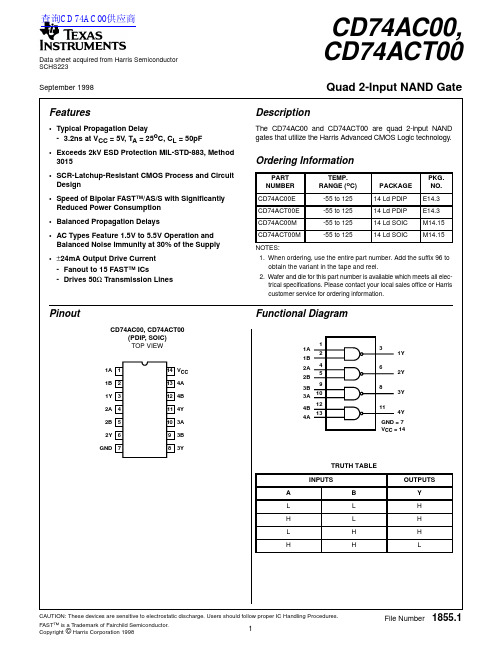
Data sheet acquired from Harris Semiconductor SCHS223Features•Typical Propagation Delay- 3.2ns at V CC = 5V , T A = 25o C, C L = 50pF•Exceeds 2kV ESD Protection MIL-STD-883, Method 3015•SCR-Latchup-Resistant CMOS Process and Circuit Design•Speed of Bipolar FAST™/AS/S with Significantly Reduced Power Consumption •Balanced Propagation Delays•AC Types Feature 1.5V to 5.5V Operation and Balanced Noise Immunity at 30% of the Supply •±24mA Output Drive Current -Fanout to 15 FAST™ ICs-Drives 50Ω Transmission LinesDescriptionThe CD74AC00and CD74ACT00are quad 2-input NAND gates that utilize the Harris Advanced CMOS Logic technology.PinoutCD74AC00, CD74ACT00(PDIP , SOIC)TOP VIEWFunctional DiagramOrdering InformationPART NUMBER TEMP.RANGE (o C)PACKAGE PKG.NO.CD74AC00E -55 to 12514 Ld PDIP E14.3CD74ACT00E -55 to 12514 Ld PDIP E14.3CD74AC00M -55 to 12514 Ld SOIC M14.15CD74ACT00M -55 to 12514 Ld SOICM14.15NOTES:1.When ordering,use the entire part number.Add the suffix 96to obtain the variant in the tape and reel.2.Wafer and die for this part number is available which meets all elec-trical specifications.Please contact your local sales office or Harris customer service for ordering information.1A 1B 1Y 2A 2B 2Y GND V CC 4A 4B 4Y 3A 3B 3Y1234567141312111098TRUTH TABLEINPUTSOUTPUTSA B Y L L H H L H L H H HHL1A 1B 2A 2B 3B 3A 4B 4A12459101213368111Y 2Y3Y 4YGND = 7V CC = 14September 1998CAUTION: These devices are sensitive to electrostatic discharge. Users should follow proper IC Handling Procedures.CD74AC00,CD74ACT00Quad 2-Input NAND GateFile Number1855.1查询CD74AC00供应商Absolute Maximum Ratings Thermal InformationDC Supply Voltage, V CC. . . . . . . . . . . . . . . . . . . . . . . .-0.5V to 6V DC Input Diode Current, I IKFor V I < -0.5V or V I > V CC + 0.5V. . . . . . . . . . . . . . . . . . . . . .±20mA DC Output Diode Current, I OKFor V O < -0.5V or V O > V CC + 0.5V . . . . . . . . . . . . . . . . . . . .±50mA DC Output Source or Sink Current per Output Pin, I OFor V O > -0.5V or V O < V CC + 0.5V . . . . . . . . . . . . . . . . . . . .±50mA DC V CC or Ground Current, I CC or I GND (Note 3) . . . . . . . . .±100mA Operating ConditionsTemperature Range, T A . . . . . . . . . . . . . . . . . . . . . .-55o C to 125o C Supply Voltage Range, V CC (Note 4)AC T ypes. . . . . . . . . . . . . . . . . . . . . . . . . . . . . . . . . . .1.5V to 5.5V ACT T ypes . . . . . . . . . . . . . . . . . . . . . . . . . . . . . . . . .4.5V to 5.5V DC Input or Output Voltage, V I, V O . . . . . . . . . . . . . . . . .0V to V CC Input Rise and Fall Slew Rate, dt/dvAC T ypes, 1.5V to 3V . . . . . . . . . . . . . . . . . . . . . . . . .50ns (Max) AC T ypes, 3.6V to 5.5V. . . . . . . . . . . . . . . . . . . . . . . .20ns (Max) ACT T ypes, 4.5V to 5.5V. . . . . . . . . . . . . . . . . . . . . . .10ns (Max)Thermal Resistance (T ypical, Note 5)θJA (o C/W) PDIP Package. . . . . . . . . . . . . . . . . . . . . . . . . . . . .90 SOIC Package. . . . . . . . . . . . . . . . . . . . . . . . . . . . .175 Maximum Junction T emperature (Plastic Package) . . . . . . . . . .150o C Maximum Storage Temperature Range . . . . . . . . . .-65o C to 150o C Maximum Lead Temperature (Soldering 10s). . . . . . . . . . . . .300o CCAUTION:Stresses above those listed in“Absolute Maximum Ratings”may cause permanent damage to the device.This is a stress only rating and operation of the device at these or any other conditions above those indicated in the operational sections of this specification is not implied.NOTES:3.For up to 4 outputs per device, add±25mA for each additional output.4.Unless otherwise specified, all voltages are referenced to ground.5.θJA is measured with the component mounted on an evaluation PC board in free air.DC Electrical SpecificationsPARAMETER SYMBOLTESTCONDITIONS VCC(V)25o C-40o C TO85o C-55o C TO125o CUNITS V I(V)I O(mA)MIN MAX MIN MAX MIN MAXAC TYPESHigh Level Input Voltage V IH-- 1.5 1.2- 1.2- 1.2-V3 2.1- 2.1- 2.1-V5.5 3.85- 3.85- 3.85-V Low Level Input Voltage V IL-- 1.5-0.3-0.3-0.3V3-0.9-0.9-0.9V5.5- 1.65- 1.65- 1.65V High Level Output Voltage V OH V IH or V IL-0.05 1.5 1.4- 1.4- 1.4-V-0.053 2.9- 2.9- 2.9-V-0.05 4.5 4.4- 4.4- 4.4-V-43 2.58- 2.48- 2.4-V-24 4.5 3.94- 3.8- 3.7-V-75(Note 6, 7)5.5-- 3.85---V-50(Note 6, 7)5.5---- 3.85-VLow Level Output VoltageV OLV IH or V IL0.05 1.5-0.1-0.1-0.1V 0.053-0.1-0.1-0.1V 0.05 4.5-0.1-0.1-0.1V 123-0.36-0.44-0.5V 24 4.5-0.36-0.44-0.5V 75(Note 6, 7) 5.5--- 1.65--V 50(Note 6, 7)5.5----- 1.65V Input Leakage Current I I V CC or GND - 5.5-±0.1-±1-±1µA Quiescent Supply Current,SSI I CCV CC or GND5.5-4-40-80µAACT TYPESHigh Level Input Voltage V IH -- 4.5 to 5.52-2-2-V Low Level Input Voltage V IL -- 4.5 to 5.5-0.8-0.8-0.8V High Level Output VoltageV OHV IH or V IL-0.05 4.5 4.4- 4.4- 4.4-V -24 4.5 3.94- 3.8- 3.7-V -75 5.5-- 3.85---V -505.5---- 3.85-V Low Level Output VoltageV OLV IH or V IL0.05 4.5-0.1-0.1-0.1V 24 4.5-0.36-0.44-0.5V 75(Note 6, 7) 5.5--- 1.65--V 50(Note 6, 7)5.5----- 1.65V Input Leakage Current I I V CC or GND - 5.5-±0.1-±1-±1µA Quiescent Supply Current,SSII CC V CC or GND 0 5.5-4-40-80µA Additional Supply Current per Input Pin TTL Inputs High 1 Unit Load ∆I CCV CC -2.1- 4.5 to 5.5- 2.4- 2.8-3mANOTES:6.Test one output at a time for a 1-second maximum duration.Measurement is made by forcing current and measuring voltage to minimize power dissipation.7.Test verifies a minimum 50Ω transmission-line-drive capability at 85o C, 75Ω at 125o C.ACT Input Load TableINPUT UNIT LOADAll0.15NOTE:Unit load is ∆I CC limit specified in DC Electrical Specifications T able, e.g., 2.4mA max at 25o C.DC Electrical Specifications(Continued)PARAMETERSYMBOL TEST CONDITIONSV CC (V)25o C -40o C TO 85o C -55o C TO 125o C UNITS V I (V)I O (mA)MIN MAX MIN MAX MIN MAXSwitching Specifications Input t r , t f = 3ns, C L = 50pF (Worst Case)PARAMETERSYMBOLV CC (V)-40o C TO 85o C-55o C TO 125o CUNITSMIN TYPMAXMINTYPMAXAC TYPESPropagation Delay, Input to Outputt PLH , t PHL1.5--83--91ns 3.3(Note 9)2.7-9.3 2.6-10.2ns 5(Note 10)1.9- 6.6 1.8-7.3ns Input CapacitanceC I ---10--10pF Power Dissipation Capacitance C PD (Note 11)--45--45-pFACT TYPESPropagation Delay, Input to Outputt PHL 5(Note 10)2.8-8 2.7-8ns t PLH3.4-9.5 3.3-9.5ns Input CapacitanceC I ---10--10pF Power Dissipation Capacitance C PD (Note 11)--45--45-pFNOTES:8.Limits tested at 100%.9.3.3V Min at 3.6V, Max at 3V.10.5V Min at 5.5V, Max at 4.5V.11.C PD is used to determine the dynamic power consumption per gate.AC: P D = V CC 2 f i (C PD + C L )ACT: P D = V CC 2 f i (C PD + C L ) + V CC ∆I CC where f i = input frequency, C L = output load capacitance, V CC = supply voltage.DUT OUTPUTR L (NOTE)OUTPUT LOAD500ΩC L 50pFNOTE:For AC Series Only: When V CC = 1.5V , R L = 1k Ω.FIGURE 1.PROPAGATION DELAY TIMESCD74ACCD74ACTInput LevelV CC 3V Input Switching Voltage, V S 0.5 V CC 1.5V Output Switching Voltage, V S0.5 V CC0.5 V CCFIGURE 2.WAVEFORMSt r = 3ns t f = 3ns90%V S 10%GNDINPUT t PHLt PLHV SLEVEL V I V OIMPORTANT NOTICETexas Instruments and its subsidiaries (TI) reserve the right to make changes to their products or to discontinue any product or service without notice, and advise customers to obtain the latest version of relevant information to verify, before placing orders, that information being relied on is current and complete. All products are sold subject to the terms and conditions of sale supplied at the time of order acknowledgement, including those pertaining to warranty, patent infringement, and limitation of liability.TI warrants performance of its semiconductor products to the specifications applicable at the time of sale in accordance with TI’s standard warranty. Testing and other quality control techniques are utilized to the extent TI deems necessary to support this warranty. Specific testing of all parameters of each device is not necessarily performed, except those mandated by government requirements.CERTAIN APPLICATIONS USING SEMICONDUCTOR PRODUCTS MAY INVOLVE POTENTIAL RISKS OF DEATH, PERSONAL INJURY, OR SEVERE PROPERTY OR ENVIRONMENTAL DAMAGE (“CRITICAL APPLICATIONS”). TI SEMICONDUCTOR PRODUCTS ARE NOT DESIGNED, AUTHORIZED, OR WARRANTED TO BE SUITABLE FOR USE IN LIFE-SUPPORT DEVICES OR SYSTEMS OR OTHER CRITICAL APPLICATIONS. INCLUSION OF TI PRODUCTS IN SUCH APPLICATIONS IS UNDERSTOOD TO BE FULLY AT THE CUSTOMER’S RISK.In order to minimize risks associated with the customer’s applications, adequate design and operating safeguards must be provided by the customer to minimize inherent or procedural hazards.TI assumes no liability for applications assistance or customer product design. TI does not warrant or represent that any license, either express or implied, is granted under any patent right, copyright, mask work right, or other intellectual property right of TI covering or relating to any combination, machine, or process in which such semiconductor products or services might be or are used. TI’s publication of information regarding any third party’s products or services does not constitute TI’s approval, warranty or endorsement thereof.Copyright © 1999, Texas Instruments Incorporated。

1/11July 2001sHIGH SPEED:t PD = 21ns (TYP .) at V CC = 4.5V sLOW POWER DISSIPATION:I CC = 4µA(MAX.) at T A =25°CsCOMPATIBLE WITH TTL OUTPUTS : V IH = 2V (MIN.) V IL = 0.8V (MAX)sBALANCED PROPAGATION DELAYS:t PLH ≅ t PHLsSYMMETRICAL OUTPUT IMPEDANCE:|I OH | = I OL = 6mA (MIN)sPIN AND FUNCTION COMPATIBLE WITH 74 SERIES 573DESCRIPTIONThe M74HCT573 is an high speed CMOS OCTAL LATCH WITH 3-STATE OUTPUTS fabricated with silicon gate C 2MOS technology.This 8-BIT D-Type latches is controlled by a latch enable input (LE) and output enable input (OE).While the LE input is held at a high level, the Q outputs will follow the data input precisely. When the LE is taken low, the Q outputs will be latched precisely at the logic level of D input data.While the OE input is at low level, the eight outputs will be in a normal logic state (high or low logic level) and while OE is at high level the outputs will be in a high impedance state.The 3-State output configuration and the wide choice of outline make bus organized system simple.The M74HCT573 is designed to directly interface HSC 2MOS systems with TTL and NMOS components.All inputs are equipped with protection circuits against static discharge and transient excess voltage.M74HCT573OCTAL D-TYPE LATCHWITH 3 STATE OUTPUT NON INVERTINGPIN CONNECTION AND IEC LOGIC SYMBOLSORDER CODESPACKAGE TUBE T & RDIP M74HCT573B1R SOP M74HCT573M1RM74HCT573RM13TR TSSOPM74HCT573TTRM74HCT5732/11INPUT AND OUTPUT EQUIVALENT CIRCUITPIN DESCRIPTIONTRUTH TABLEX: Don’t CareZ: High Impedance(*): Q Outputs are latched at the time when the LE input is taken low logic level.LOGIC DIAGRAMPIN No SYMBOL NAME AND FUNCTION 1OE 3 State Output Enable Input (Active LOW)2, 3, 4, 5, 6, 7, 8, 9D0 to D7Data Inputs12, 13, 14, 15, 16, 17, 18, 19Q0 to Q73 State Latch Outputs11LE Latch Enable Input 10GND Ground (0V)20V CCPositive Supply VoltageINPUTSOUTPUTSOE LE D QH X X ZL L X NO CHANGE (*)L H L L LHHHM74HCT5733/11ABSOLUTE MAXIMUM RATINGSAbsolute Maximum Ratings are those values beyond which damage to the device may occur. Functional operation under these conditions is not implied(*) 500mW at 65 °C; derate to 300mW by 10mW/°C from 65°C to 85°CRECOMMENDED OPERATING CONDITIONSSymbol ParameterValue Unit V CC Supply Voltage -0.5 to +7V V I DC Input Voltage -0.5 to V CC + 0.5V V O DC Output Voltage -0.5 to V CC + 0.5V I IK DC Input Diode Current ± 20mA I OK DC Output Diode Current ± 20mA I O DC Output Current ± 35mA I CC or I GND DC V CC or Ground Current± 70mA P D Power Dissipation 500(*)mW T stg Storage Temperature -65 to +150°C T LLead Temperature (10 sec)300°CSymbol ParameterValue Unit V CC Supply Voltage 4.5 to 5.5V V I Input Voltage 0 to V CC V V O Output Voltage 0 to V CC V T op Operating Temperature-55 to 125°C t r , t fInput Rise and Fall Time (V CC = 4.5 to 5.5V)0 to 500nsM74HCT5734/11DC SPECIFICATIONSAC ELECTRICAL CHARACTERISTICS (C L = 50 pF, Input t r = t f = 6ns)SymbolParameterTest ConditionValue UnitV CC (V)T A = 25°C -40 to 85°C -55 to 125°C Min.Typ.Max.Min.Max.Min.Max.V IHHigh Level Input Voltage4.5 to5.5 2.02.02.0V V IL Low Level Input Voltage4.5 to5.50.80.80.8V V OH High Level Output Voltage4.5I O =-20 µA 4.4 4.5 4.4 4.4VI O =-6.0 mA 4.184.31 4.134.10V OL Low Level Output Voltage4.5I O =20 µA 0.00.10.10.1V I O =6.0 mA 0.170.260.330.40I I Input Leakage Current5.5V I = V CC or GND ± 0.1± 1± 1µA I OZ High Impedance Output Leakage Current5.5V I = V IH or V IL V O = V CC or GND ± 0.5± 5± 10µA I CC Quiescent Supply Current5.5V I = V CC or GND 44080µA ∆ I CCAdditional Worst Case Supply Current5.5Per Input pin V I = 0.5V or V I = 2.4V Other Inputs at V CC or GND2.02.93.0mASymbolParameterTest ConditionValue UnitV CC (V)C L (pF)T A = 25°C -40 to 85°C -55 to 125°C Min.Typ.Max.Min.Max.Min.Max.t TLH t THL Output TransitionTime4.5507121518ns t PLH t PHL Propagation DelayTime (LE - Q,Q) 4.55021334150ns 4.515025394959t PLH t PHL Propagation DelayTime (D - Q,Q) 4.55019303845ns 4.515023364554t PZL t PZH Output EnableTime 4.550R L = 1 K Ω19303845ns 4.515023364554t PLZ t PHZ Output DisableTime4.550R L = 1 K Ω18253138ns t W(L) t W(H)Minimum PulseWidth (LE) 4.5507151922ns t s Minimum Set-Up Time4.5504101315ns t hMinimum Hold Time4.550555nsM74HCT5735/11CAPACITIVE CHARACTERISTICS1) C PD is defined as the value of the IC’s internal equivalent capacitance which is calculated from the operating current consumption without load. (Refer to Test Circuit). Average operating current can be obtained by the following equation. I CC(opr) = C PD x V CC x f IN + I CC /8 (per Flip Flop)TEST CIRCUITC L = 50pF/150pF or equivalent (includes jig and probe capacitance)R 1 = 1K Ω or equivalentR T = Z OUT of pulse generator (typically 50Ω)SymbolParameterTest ConditionValue UnitV CC (V)T A = 25°C -40 to 85°C -55 to 125°C Min.Typ.Max.Min.Max.Min.Max.C IN Input Capacitance5101010pF C OUT OutputCapacitance10pF C PDPower Dissipation Capacitance (note 1)51pF TESTSWITCH t PLH , t PHL Open t PZL , t PLZ V CC t PZH , t PHZGNDM74HCT5736/11WAVEFORM 1: LE TO Qn PROPAGATION DELAYS, LE MINIMUM PULSE WIDTH, Dn TO LE SETUP AND HOLD TIMES(f=1MHz; 50% duty cycle)M74HCT5737/11WAVEFORM 2: OUTPUT ENABLE AND DISABLE TIMES (f=1MHz; 50% duty cycle)WAVEFORM 3: PROPAGATION DELAY TIMES(f=1MHz; 50% duty cycle)M74HCT573 Information furnished is believed to be accurate and reliable. However, STMicroelectronics assumes no responsibility for the consequences of use of such information nor for any infringement of patents or other rights of third parties which may result from its use. No license is granted by implication or otherwise under any patent or patent rights of STMicroelectronics. Specifications mentioned in this publication are subject to change without notice. This publication supersedes and replaces all information previously supplied. STMicroelectronics products are not authorized for use as critical components in life support devices or systems without express written approval of STMicroelectronics.© The ST logo is a registered trademark of STMicroelectronics© 2000 STMicroelectronics - Printed in Italy - All Rights ReservedSTMicroelectronics GROUP OF COMPANIESAustralia - Brazil - China - Finland - France - Germany - Hong Kong - India - Italy - Japan - Malaysia - Malta - MoroccoSingapore - Spain - Sweden - Switzerland - United Kingdom© 11/11芯天下--/。

This data sheet is applicable to the CD54/74AC574 and CD54/74ACT574. The CD54/74AC564 and CD54/74ACT564 were not acquired from Harris Semiconductor.Data sheet acquired from Harris Semiconductor SCHS292IMPORTANT NOTICETexas Instruments and its subsidiaries (TI) reserve the right to make changes to their products or to discontinue any product or service without notice, and advise customers to obtain the latest version of relevant information to verify, before placing orders, that information being relied on is current and complete. All products are sold subject to the terms and conditions of sale supplied at the time of order acknowledgement, including those pertaining to warranty, patent infringement, and limitation of liability.TI warrants performance of its semiconductor products to the specifications applicable at the time of sale in accordance with TI’s standard warranty. Testing and other quality control techniques are utilized to the extent TI deems necessary to support this warranty. Specific testing of all parameters of each device is not necessarily performed, except those mandated by government requirements.CERTAIN APPLICATIONS USING SEMICONDUCTOR PRODUCTS MAY INVOLVE POTENTIAL RISKS OF DEATH, PERSONAL INJURY, OR SEVERE PROPERTY OR ENVIRONMENTAL DAMAGE (“CRITICAL APPLICATIONS”). TI SEMICONDUCTOR PRODUCTS ARE NOT DESIGNED, AUTHORIZED, OR WARRANTED TO BE SUITABLE FOR USE IN LIFE-SUPPORT DEVICES OR SYSTEMS OR OTHER CRITICAL APPLICATIONS. INCLUSION OF TI PRODUCTS IN SUCH APPLICATIONS IS UNDERSTOOD TO BE FULLY AT THE CUSTOMER’S RISK.In order to minimize risks associated with the customer’s applications, adequate design and operating safeguards must be provided by the customer to minimize inherent or procedural hazards.TI assumes no liability for applications assistance or customer product design. TI does not warrant or represent that any license, either express or implied, is granted under any patent right, copyright, mask work right, or other intellectual property right of TI covering or relating to any combination, machine, or process in which such semiconductor products or services might be or are used. TI’s publication of information regarding any third party’s products or services does not constitute TI’s approval, warranty or endorsement thereof.Copyright © 1998, Texas Instruments Incorporated。

常用74系列标准数字电路的中文名称资料器件代号器件名称74 74LS 74HC00 四2输入端与非门√ √ √01 四2输入端与非门(OC) √ √02 四2输入端或非门√ √ √03 四2输入端与非门(OC) √ √04 六反相器√ √ √05 六反相器(OC) √ √06 六高压输出反相器(OC,30V) √ √07 六高压输出缓冲,驱动器(OC,30V) √ √ √08 四2输入端与门√ √ √09 四2输入端与门(OC) √ √ √10 三3输入端与非门√ √ √11 三3输入端与门√ √12 三3输入端与非门(OC) √ √ √13 双4输入端与非门√ √ √14 六反相器√ √ √15 三3输入端与门(OC) √ √16 六高压输出反相器(OC,15V) √17 六高压输出缓冲,驱动器(OC,15V) √20 双4输入端与非门√ √ √21 双4输入端与门√ √ √22 双4输入端与非门(OC) √ √25 双4输入端或非门(有选通端) √ √ √26 四2输入端高压输出与非缓冲器√ √ √27 三3输入端或非门√ √ √28 四2输入端或非缓冲器√ √ √30 8输入端与非门√ √ √32 四2输入端或门√ √ √33 四2输入端或非缓冲器(OC) √ √37 四2输入端与非缓冲器√ √38 四2输入端与非缓冲器(OC) √ √40 双4输入端与非缓冲器√ √ √42 4线-10线译码器(BCD输入) √ √43 4线-10线译码器(余3码输入) √44 4线-10线译码器(余3葛莱码输入) √48 4线-7段译码器√49 4线-7段译码器√50 双2路2-2输入与或非门√ √ √51 2路3-3输入,2路2-2输入与或非门√ √ √52 4路2-3-2-2输入与或门√53 4路2-2-2-2输入与或非门√54 4路2-3-3-2输入与或非门√ √55 2路4-4输入与或非门√60 双4输入与扩展器√ √61 三3输入与扩展器√62 4路2-3-3-2输入与或扩展器√64 4路4-2-3-2输入与或非门√65 4路4-2-3-2输入与或非门(OC) √70 与门输入J-K触发器√71 与或门输入J-K触发器√72 与门输入J-K触发器√74 双上升沿D型触发器√ √78 双D型触发器√ √85 四位数值比较器√86 四2输入端异或门√ √ √87 4位二进制原码/反码√95 4位移位寄存器√101 与或门输入J-K触发器√102 与门输入J-K触发器√107 双主-从J-K触发器√108 双主-从J-K触发器√109 双主-从J-K触发器√110 与门输入J-K触发器√111 双主-从J-K触发器√ √112 双下降沿J-K触发器√113 双下降沿J-K触发器√114 双下降沿J-K触发器√116 双4位锁存器√120 双脉冲同步驱动器√121 单稳态触发器√ √ √122 可重触发单稳态触发器√ √ √123 可重触发双稳态触发器√ √ √125 四总线缓冲器√ √ √126 四总线缓冲器√ √ √128 四2输入端或非线驱动器√ √ √132 四2输入端与非门√ √ √常用4000系列标准数字电路的中文名称资料型号器件名称厂牌备注CD4000 双3输入端或非门+单非门TICD4001 四2输入端或非门HIT/NSC/TI/GOLCD4002 双4输入端或非门NSCCD4006 18位串入/串出移位寄存器NSCCD4007 双互补对加反相器NSCCD4008 4位超前进位全加器NSCCD4009 六反相缓冲/变换器NSCCD4010 六同相缓冲/变换器NSCCD4011 四2输入端与非门HIT/TICD4012 双4输入端与非门NSCCD4013 双主-从D型触发器FSC/NSC/TOSCD4014 8位串入/并入-串出移位寄存器NSCCD4015 双4位串入/并出移位寄存器TICD4016 四传输门FSC/TICD4017 十进制计数/分配器FSC/TI/MOTCD4018 可预制1/N计数器NSC/MOTCD4019 四与或选择器PHICD4020 14级串行二进制计数/分频器FSCCD4021 08位串入/并入-串出移位寄存器PHI/NSCCD4022 八进制计数/分配器NSC/MOTCD4023 三3输入端与非门NSC/MOT/TICD4024 7级二进制串行计数/分频器NSC/MOT/TICD4025 三3输入端或非门NSC/MOT/TICD4026 十进制计数/7段译码器NSC/MOT/TICD4027 双J-K触发器NSC/MOT/TICD4028 BCD码十进制译码器NSC/MOT/TICD4029 可预置可逆计数器NSC/MOT/TICD4030 四异或门NSC/MOT/TI/GOLCD4031 64位串入/串出移位存储器NSC/MOT/TICD4032 三串行加法器NSC/TICD4033 十进制计数/7段译码器NSC/TICD4034 8位通用总线寄存器NSC/MOT/TICD4035 4位并入/串入-并出/串出移位寄存NSC/MOT/TI CD4038 三串行加法器NSC/TICD4040 12级二进制串行计数/分频器NSC/MOT/TICD4041 四同相/反相缓冲器NSC/MOT/TICD4042 四锁存D型触发器NSC/MOT/TICD4043 4三态R-S锁存触发器("1"触发) NSC/MOT/TI CD4044 四三态R-S锁存触发器("0"触发) NSC/MOT/TI CD4046 锁相环NSC/MOT/TI/PHICD4047 无稳态/单稳态多谐振荡器NSC/MOT/TICD4048 4输入端可扩展多功能门NSC/HIT/TICD4049 六反相缓冲/变换器NSC/HIT/TICD4050 六同相缓冲/变换器NSC/MOT/TICD4051 八选一模拟开关NSC/MOT/TICD4052 双4选1模拟开关NSC/MOT/TICD4053 三组二路模拟开关NSC/MOT/TICD4054 液晶显示驱动器NSC/HIT/TICD4055 BCD-7段译码/液晶驱动器NSC/HIT/TI CD4056 液晶显示驱动器NSC/HIT/TICD4059 “N”分频计数器NSC/TICD4060 14级二进制串行计数/分频器NSC/TI/MOT CD4063 四位数字比较器NSC/HIT/TICD4066 四传输门NSC/TI/MOTCD4067 16选1模拟开关NSC/TICD4068 八输入端与非门/与门NSC/HIT/TICD4069 六反相器NSC/HIT/TICD4070 四异或门NSC/HIT/TICD4071 四2输入端或门NSC/TICD4072 双4输入端或门NSC/TICD4073 三3输入端与门NSC/TICD4075 三3输入端或门NSC/TICD4076 四D寄存器CD4077 四2输入端异或非门HITCD4078 8输入端或非门/或门CD4081 四2输入端与门NSC/HIT/TICD4082 双4输入端与门NSC/HIT/TICD4085 双2路2输入端与或非门CD4086 四2输入端可扩展与或非门CD4089 二进制比例乘法器CD4093 四2输入端施密特触发器NSC/MOT/ST CD4094 8位移位存储总线寄存器NSC/TI/PHICD4095 3输入端J-K触发器CD4096 3输入端J-K触发器CD4097 双路八选一模拟开关CD4098 双单稳态触发器NSC/MOT/TICD4099 8位可寻址锁存器NSC/MOT/STCD40100 32位左/右移位寄存器CD40101 9位奇偶较验器CD40102 8位可预置同步BCD减法计数器CD40103 8位可预置同步二进制减法计数器CD40104 4位双向移位寄存器CD40105 先入先出FI-FD寄存器CD40106 六施密特触发器NSC\TICD40107 双2输入端与非缓冲/驱动器HAR\TICD40108 4字×4位多通道寄存器CD40109 四低-高电平位移器CD40110 十进制加/减,计数,锁存,译码驱动STCD40147 10-4线编码器NSC\MOTCD40160 可预置BCD加计数器NSC\MOTCD40161 可预置4位二进制加计数器NSC\MOTCD40162 BCD加法计数器NSC\MOTCD40163 4位二进制同步计数器NSC\MOTCD40174 六锁存D型触发器NSC\TI\MOTCD40175 四D型触发器NSC\TI\MOTCD40181 4位算术逻辑单元/函数发生器CD40182 超前位发生器CD40192 可预置BCD加/减计数器(双时钟) NSC\TI CD40193 可预置4位二进制加/减计数器NSC\TICD40194 4位并入/串入-并出/串出移位寄存NSC\MOT CD40195 4位并入/串入-并出/串出移位寄存NSC\MOT CD40208 4×4多端口寄存器CD4501 4输入端双与门及2输入端或非门CD4502 可选通三态输出六反相/缓冲器CD4503 六同相三态缓冲器CD4504 六电压转换器CD4506 双二组2输入可扩展或非门CD4508 双4位锁存D型触发器CD4510 可预置BCD码加/减计数器CD4511 BCD锁存,7段译码,驱动器CD4512 八路数据选择器CD4513 BCD锁存,7段译码,驱动器(消隐)CD4514 4位锁存,4线-16线译码器CD4515 4位锁存,4线-16线译码器CD4516 可预置4位二进制加/减计数器CD4517 双64位静态移位寄存器CD4518 双BCD同步加计数器CD4519 四位与或选择器CD4520 双4位二进制同步加计数器CD4521 24级分频器CD4522 可预置BCD同步1/N计数器CD4526 可预置4位二进制同步1/N计数器CD4527 BCD比例乘法器CD4528 双单稳态触发器CD4529 双四路/单八路模拟开关CD4530 双5输入端优势逻辑门CD4531 12位奇偶校验器CD4532 8位优先编码器CD4536 可编程定时器CD4538 精密双单稳CD4539 双四路数据选择器CD4541 可编程序振荡/计时器CD4543 BCD七段锁存译码,驱动器CD4544 BCD七段锁存译码,驱动器CD4547 BCD七段译码/大电流驱动器CD4549 函数近似寄存器CD4551 四2通道模拟开关CD4553 三位BCD计数器CD4555 双二进制四选一译码器/分离器CD4556 双二进制四选一译码器/分离器CD4558 BCD八段译码器CD4560 "N"BCD加法器CD4561 "9"求补器CD4573 四可编程运算放大器CD4574 四可编程电压比较器CD4575 双可编程运放/比较器CD4583 双施密特触发器CD4584 六施密特触发器CD4585 4位数值比较器CD4599 8位可寻址锁存器CD22100 4×4×1交叉点开关。

PACKAGING INFORMATIONOrderable Device Status (1)Package Type Package DrawingPins Package Qty Eco Plan (2)Lead/Ball FinishMSL Peak Temp (3)CD54HC573F ACTIVE CDIP J 201TBD A42N /A for Pkg Type CD54HC573F3A ACTIVE CDIP J 201TBD A42N /A for Pkg Type CD74HC573E ACTIVE PDIP N 2020Pb-Free (RoHS)CU NIPDAU N /A for Pkg Type CD74HC573EE4ACTIVE PDIP N 2020Pb-Free (RoHS)CU NIPDAU N /A for Pkg Type CD74HC573M ACTIVE SOIC DW 2025Green (RoHS &no Sb/Br)CU NIPDAU Level-1-260C-UNLIM CD74HC573M96ACTIVE SOIC DW 202000Green (RoHS &no Sb/Br)CU NIPDAU Level-1-260C-UNLIM CD74HC573M96G4ACTIVE SOIC DW 202000Green (RoHS &no Sb/Br)CU NIPDAU Level-1-260C-UNLIM CD74HC573MG4ACTIVESOICDW2025Green (RoHS &no Sb/Br)CU NIPDAULevel-1-260C-UNLIM(1)The marketing status values are defined as follows:ACTIVE:Product device recommended for new designs.LIFEBUY:TI has announced that the device will be discontinued,and a lifetime-buy period is in effect.NRND:Not recommended for new designs.Device is in production to support existing customers,but TI does not recommend using this part in a new design.PREVIEW:Device has been announced but is not in production.Samples may or may not be available.OBSOLETE:TI has discontinued the production of the device.(2)Eco Plan -The planned eco-friendly classification:Pb-Free (RoHS),Pb-Free (RoHS Exempt),or Green (RoHS &no Sb/Br)-please check /productcontent for the latest availability information and additional product content details.TBD:The Pb-Free/Green conversion plan has not been defined.Pb-Free (RoHS):TI's terms "Lead-Free"or "Pb-Free"mean semiconductor products that are compatible with the current RoHS requirements for all 6substances,including the requirement that lead not exceed 0.1%by weight in homogeneous materials.Where designed to be soldered at high temperatures,TI Pb-Free products are suitable for use in specified lead-free processes.Pb-Free (RoHS Exempt):This component has a RoHS exemption for either 1)lead-based flip-chip solder bumps used between the die and package,or 2)lead-based die adhesive used between the die andleadframe.The component is otherwise considered Pb-Free (RoHS compatible)as defined above.Green (RoHS &no Sb/Br):TI defines "Green"to mean Pb-Free (RoHS compatible),and free of Bromine (Br)and Antimony (Sb)based flame retardants (Br or Sb do not exceed 0.1%by weight in homogeneous material)(3)MSL,Peak Temp.--The Moisture Sensitivity Level rating according to the JEDEC industry standard classifications,and peak solder temperature.Important Information and Disclaimer:The information provided on this page represents TI's knowledge and belief as of the date that it is provided.TI bases its knowledge and belief on information provided by third parties,and makes no representation or warranty as to the accuracy of such information.Efforts are underway to better integrate information from third parties.TI has taken and continues to take reasonable steps to provide representative and accurate information but may not have conducted destructive testing or chemical analysis on incoming materials and chemicals.TI and TI suppliers consider certain information to be proprietary,and thus CAS numbers and other limited information may not be available for release.In no event shall TI's liability arising out of such information exceed the total purchase price of the TI part(s)at issue in this document sold by TI to Customer on an annual basis.PACKAGE OPTION ADDENDUM15-Oct-2009TAPE AND REEL INFORMATION*All dimensions are nominalDevicePackage Type Package Drawing Pins SPQReel Diameter (mm)Reel Width W1(mm)A0(mm)B0(mm)K0(mm)P1(mm)W (mm)Pin1Quadrant CD74HC573M96SOICDW202000330.024.410.813.02.712.024.0Q1*All dimensions are nominalDevice Package Type Package Drawing Pins SPQ Length(mm)Width(mm)Height(mm)CD74HC573M96SOIC DW202000367.0367.045.0IMPORTANT NOTICETexas Instruments Incorporated and its subsidiaries(TI)reserve the right to make corrections,enhancements,improvements and other changes to its semiconductor products and services per JESD46C and to discontinue any product or service per JESD48B.Buyers should obtain the latest relevant information before placing orders and should verify that such information is current and complete.All semiconductor products(also referred to herein as“components”)are sold subject to TI’s terms and conditions of sale supplied at the time of order acknowledgment.TI warrants performance of its components to the specifications applicable at the time of sale,in accordance with the warranty in TI’s terms and conditions of sale of semiconductor products.Testing and other quality control techniques are used to the extent TI deems necessary to support this warranty.Except where mandated by applicable law,testing of all parameters of each component is not necessarily performed.TI assumes no liability for applications assistance or the design of Buyers’products.Buyers are responsible for their products and applications using TI components.To minimize the risks associated with Buyers’products and applications,Buyers should provide adequate design and operating safeguards.TI does not warrant or represent that any license,either express or implied,is granted under any patent right,copyright,mask work right,or other intellectual property right relating to any combination,machine,or process in which TI components or services are rmation published by TI regarding third-party products or services does not constitute a license to use such products or services or a warranty or endorsement e of such information may require a license from a third party under the patents or other intellectual property of the third party,or a license from TI under the patents or other intellectual property of TI.Reproduction of significant portions of TI information in TI data books or data sheets is permissible only if reproduction is without alteration and is accompanied by all associated warranties,conditions,limitations,and notices.TI is not responsible or liable for such altered rmation of third parties may be subject to additional restrictions.Resale of TI components or services with statements different from or beyond the parameters stated by TI for that component or service voids all express and any implied warranties for the associated TI component or service and is an unfair and deceptive business practice. TI is not responsible or liable for any such statements.Buyer acknowledges and agrees that it is solely responsible for compliance with all legal,regulatory and safety-related requirements concerning its products,and any use of TI components in its applications,notwithstanding any applications-related information or support that may be provided by TI.Buyer represents and agrees that it has all the necessary expertise to create and implement safeguards which anticipate dangerous consequences of failures,monitor failures and their consequences,lessen the likelihood of failures that might cause harm and take appropriate remedial actions.Buyer will fully indemnify TI and its representatives against any damages arising out of the use of any TI components in safety-critical applications.In some cases,TI components may be promoted specifically to facilitate safety-related applications.With such components,TI’s goal is to help enable customers to design and create their own end-product solutions that meet applicable functional safety standards and requirements.Nonetheless,such components are subject to these terms.No TI components are authorized for use in FDA Class III(or similar life-critical medical equipment)unless authorized officers of the parties have executed a special agreement specifically governing such use.Only those TI components which TI has specifically designated as military grade or“enhanced plastic”are designed and intended for use in military/aerospace applications or environments.Buyer acknowledges and agrees that any military or aerospace use of TI components which have not been so designated is solely at the Buyer's risk,and that Buyer is solely responsible for compliance with all legal and regulatory requirements in connection with such use.TI has specifically designated certain components which meet ISO/TS16949requirements,mainly for automotive ponents which have not been so designated are neither designed nor intended for automotive use;and TI will not be responsible for any failure of such components to meet such requirements.Products ApplicationsAudio /audio Automotive and Transportation /automotiveAmplifiers Communications and Telecom /communicationsData Converters Computers and Peripherals /computersDLP®Products Consumer Electronics /consumer-appsDSP Energy and Lighting /energyClocks and Timers /clocks Industrial /industrialInterface Medical /medicalLogic Security /securityPower Mgmt Space,Avionics and Defense /space-avionics-defense Microcontrollers Video and Imaging /videoRFID OMAP Mobile Processors /omap TI E2E Community Wireless Connectivity /wirelessconnectivityMailing Address:Texas Instruments,Post Office Box655303,Dallas,Texas75265Copyright©2012,Texas Instruments Incorporated。

74ls573中文资料三态总线驱动输出·置数全并行存取·缓冲控制输入·使能输入有改善抗扰度的滞后作用原理:74LS573 的八个锁存器都是透明的D 型锁存器,当使能(G)为高时,Q 输出将随数据(D)输入而变。
当使能为低时,输出将锁存在已建立的数据电平上。
输出控制不影响锁存器的内部工作,即老数据可以保持,甚至当输出被关闭时,新的数据也可以置入。
这种电路可以驱动大电容或低阻抗负载,可以直接与系统总线接口并驱动总线,而不需要外接口。
特别适用于缓冲寄存器,I/O 通道,双向总线驱动器和工作寄存器。
H=高电平 L=低电平×=不定 Z=高阻态QO=建立稳态输入条件前Q的电平引脚图及功能图Operating Conditions 操作条件Symbol 符号Parameter 参数DM74LS最小典型最大VCC Supply Voltage 电源电压 4.75 5 5.25VIH High Level Input Voltage输入高电平电压 2 - -VIL LOW Level Input Voltage 输入低电平电压- - 0.8IOH HIGH Level Input Current输入高电平电流- - −2.6IOL LOW Level Output Current低电平输出电流- - 24TA Free Air Operating Temperature工作温度0 - 70Note 1: The “Absolute Maximum Ratings” are those values beyond which the safety of th cannot be guaranteed. The device should not be operated at these limits. The parametri defined in the “Electrical Characteristics” table are not guaranteed at the absolute ratings. The “Recommended Operating Conditions” table will define the conditions fo device operation.Electrical Characteristics 直流电气特性Over recommended operating free air temperature range (unless otherwise noted)Symbol 符号Parameter 参数Conditions 条件最小典型最大单VI Input Clamp Voltage输入钳位电压VCC=最小, II=−18 mA - - −1.5VOH High Level OutputVoltage输出高电平电压VCC = 最小, IOH=最大,VIL = 最大2.73.4 -VOL Low Level OutputVoltage输出低电平电压VCC = 最小, IOL=最大- 0.35 0.5VIH = 最小- - -。

74LV573A中⽂资料PACKAGING INFORMATIONOrderable Device Status (1)Package Type Package Drawing Pins Package Qty Eco Plan (2)Lead/Ball Finish MSL Peak Temp (3)SN74LV573ADBR ACTIVE SSOP DB 202000Green (RoHS &no Sb/Br)CU NIPDAU Level-1-260C-UNLIM SN74LV573ADBRE4ACTIVE SSOPDB 202000Green (RoHS &no Sb/Br)CU NIPDAU Level-1-260C-UNLIM SN74LV573ADGVR ACTIVE TVSOP DGV 202000Green (RoHS &no Sb/Br)CU NIPDAU Level-1-260C-UNLIM SN74LV573ADGVRE4ACTIVE TVSOP DGV 202000Green (RoHS &no Sb/Br)CU NIPDAU Level-1-260C-UNLIM SN74LV573ADW ACTIVE SOIC DW 2025Green (RoHS &no Sb/Br)CU NIPDAU Level-1-260C-UNLIM SN74LV573ADWE4ACTIVE SOIC DW 2025Green (RoHS &no Sb/Br)CU NIPDAU Level-1-260C-UNLIM SN74LV573ADWR ACTIVE SOIC DW 202000Green (RoHS &no Sb/Br)CU NIPDAU Level-1-260C-UNLIM SN74LV573ADWRE4ACTIVE SOIC DW 202000Green (RoHS &no Sb/Br)CU NIPDAU Level-1-260C-UNLIM SN74LV573AGQNRACTIVEBGA MI CROSTA R JUNI ORGQN201000TBDSNPBLevel-1-240C-UNLIMSN74LV573ANSR ACTIVE SO NS 202000Green (RoHS &no Sb/Br)CU NIPDAU Level-1-260C-UNLIM SN74LV573ANSRE4ACTIVE SO NS 202000Green (RoHS &no Sb/Br)CU NIPDAU Level-1-260C-UNLIM SN74LV573APW ACTIVE TSSOP PW 2070Green (RoHS &no Sb/Br)CU NIPDAU Level-1-260C-UNLIM SN74LV573APWE4ACTIVE TSSOP PW 2070Green (RoHS &no Sb/Br)CU NIPDAU Level-1-260C-UNLIM SN74LV573APWR ACTIVE TSSOP PW 202000Green (RoHS &no Sb/Br)CU NIPDAU Level-1-260C-UNLIM SN74LV573APWRE4ACTIVE TSSOP PW 202000Green (RoHS &no Sb/Br)CU NIPDAU Level-1-260C-UNLIM SN74LV573APWRG4ACTIVE TSSOP PW 202000Green (RoHS &no Sb/Br)CU NIPDAU Level-1-260C-UNLIM SN74LV573APWT ACTIVE TSSOP PW 20250Green (RoHS &no Sb/Br)CU NIPDAU Level-1-260C-UNLIM SN74LV573APWTE4ACTIVE TSSOP PW 20250Green (RoHS &no Sb/Br)CU NIPDAU Level-1-260C-UNLIM SN74LV573ARGYR ACTIVE QFN RGY 201000Green (RoHS &no Sb/Br)CU NIPDAU Level-2-260C-1YEAR SN74LV573ARGYRG4ACTIVE QFN RGY 201000Green (RoHS &no Sb/Br)CU NIPDAU Level-2-260C-1YEAR SN74LV573AZQNRACTIVEBGA MI CROSTA R JUNI ORZQN201000Green (RoHS &no Sb/Br)SNAGCULevel-1-260C-UNLIM(1)The marketing status values are defined as follows:ACTIVE:Product device recommended for new designs.LIFEBUY:TI has announced that the device will be discontinued,and a lifetime-buy period is in effect.NRND:Not recommended for new designs.Device is in production to support existing customers,but TI does not recommend using this part ina new design.PREVIEW:Device has been announced but is not in production.Samples may or may not be available.OBSOLETE:TI has discontinued the production of the device.(2)Eco Plan-The planned eco-friendly classification:Pb-Free(RoHS),Pb-Free(RoHS Exempt),or Green(RoHS&no Sb/Br)-please check /doc/c811093619.html/productcontent for the latest availability information and additional product content details.TBD:The Pb-Free/Green conversion plan has not been defined.Pb-Free(RoHS):TI's terms"Lead-Free"or"Pb-Free"mean semiconductor products that are compatible with the current RoHS requirements for all6substances,including the requirement that lead not exceed0.1%by weight in homogeneous materials.Where designed to be soldered at high temperatures,TI Pb-Free products are suitable for use in specified lead-free processes.Pb-Free(RoHS Exempt):This component has a RoHS exemption for either1)lead-based flip-chip solder bumps used between the die and package,or2)lead-based die adhesive used between the die and leadframe.The component is otherwise considered Pb-Free(RoHS compatible)as defined above.Green(RoHS&no Sb/Br):TI defines"Green"to mean Pb-Free(RoHS compatible),and free of Bromine(Br)andAntimony(Sb)based flame retardants(Br or Sb do not exceed0.1%by weight in homogeneous material)(3)MSL,Peak Temp.--The Moisture Sensitivity Level rating according to the JEDEC industry standard classifications,and peak solder temperature.Important Information and Disclaimer:The information provided on this page represents TI's knowledge and belief as of the date that it is provided.TI bases its knowledge and belief on information provided by third parties,and makes no representation or warranty as to the accuracy of such information.Efforts are underway to better integrate information from third parties.TI has taken and continues to take reasonable steps to provide representative and accurate information but may not have conducted destructive testing or chemical analysis on incoming materials and chemicals.TI and TI suppliers consider certain information to be proprietary,and thus CAS numbers and other limited information may not be available for release.In no event shall TI's liability arising out of such information exceed the total purchase price of the TI part(s)at issue in this document sold by TI to Customer on an annual basis.。

74ls,CD系列中文资料目录功能介绍2008-01-25 09:38:30 本文已公布到博客频道职场·创业分类在用单片机的扩展中,较多用到74LS系列器件,故收集了此系列器件资料,先贴一个74系列器件目录。
在后期应用中,再逐一详细介绍:74ls系列中文资料目录功能介绍型号功能----------------------------------------------------74ls00 2输入四与非门74ls01 2输入四与非门 (oc)74ls02 2输入四或非门74ls03 2输入四与非门 (oc)74ls04 六倒相器74ls05 六倒相器(oc)74ls06 六高压输出反相缓冲器/驱动器(oc,30v)74ls07 六高压输出缓冲器/驱动器(oc,30v)74ls08 2输入四与门74ls09 2输入四与门(oc)74ls10 3输入三与非门74ls11 3输入三与门74ls12 3输入三与非门 (oc)74ls13 4输入双与非门 (斯密特触发)74ls14 六倒相器(斯密特触发)74ls15 3输入三与门 (oc)74ls16 六高压输出反相缓冲器/驱动器(oc,15v)74ls17 六高压输出缓冲器/驱动器(oc,15v)74ls18 4输入双与非门 (斯密特触发)74ls19 六倒相器(斯密特触发)74ls20 4输入双与非门74ls21 4输入双与门74ls22 4输入双与非门(oc)74ls23 双可扩展的输入或非门74ls24 2输入四与非门(斯密特触发)74ls25 4输入双或非门(有选通)74ls26 2输入四高电平接口与非缓冲器(oc,15v)74ls27 3输入三或非门74ls28 2输入四或非缓冲器74ls30 8输入与非门74ls31 延迟电路74ls32 2输入四或门74ls33 2输入四或非缓冲器(集电极开路输出)74ls34 六缓冲器74ls35 六缓冲器(oc)74ls36 2输入四或非门(有选通)74ls37 2输入四与非缓冲器74ls38 2输入四或非缓冲器(集电极开路输出)74ls39 2输入四或非缓冲器(集电极开路输出)74ls40 4输入双与非缓冲器74ls41 bcd-十进制计数器74ls42 4线-10线译码器(bcd输入)74ls43 4线-10线译码器(余3码输入)74ls44 4线-10线译码器(余3葛莱码输入)74ls45 bcd-十进制译码器/驱动器74ls46 bcd-七段译码器/驱动器74ls47 bcd-七段译码器/驱动器74ls48 bcd-七段译码器/驱动器74ls49 bcd-七段译码器/驱动器(oc)74ls50 双二路2-2输入与或非门(一门可扩展)74ls51 双二路2-2输入与或非门74ls51 二路3-3输入,二路2-2输入与或非门74ls52 四路2-3-2-2输入与或门(可扩展)74ls53 四路2-2-2-2输入与或非门(可扩展)74ls53 四路2-2-3-2输入与或非门(可扩展)74ls54 四路2-2-2-2输入与或非门74ls54 四路2-3-3-2输入与或非门74ls54 四路2-2-3-2输入与或非门74ls55 二路4-4输入与或非门(可扩展)74ls60 双四输入与扩展74ls61 三3输入与扩展74ls62 四路2-3-3-2输入与或扩展器74ls63 六电流读出接口门74ls64 四路4-2-3-2输入与或非门74ls65 四路4-2-3-2输入与或非门(oc)74ls70 与门输入上升沿jk触发器74ls71 与输入r-s主从触发器74ls72 与门输入主从jk触发器74ls73 双j-k触发器(带清除端)74ls74 正沿触发双d型触发器(带预置端和清除端)74ls75 4位双稳锁存器74ls76 双j-k触发器(带预置端和清除端)74ls77 4位双稳态锁存器74ls78 双j-k触发器(带预置端,公共清除端和公共时钟端) 74ls80 门控全加器74ls81 16位随机存取存储器74ls82 2位二进制全加器(快速进位)74ls83 4位二进制全加器(快速进位)74ls84 16位随机存取存储器74ls85 4位数字比较器74ls86 2输入四异或门74ls87 四位二进制原码/反码/oi单元74ls89 64位读/写存储器74ls90 十进制计数器74ls91 八位移位寄存器74ls92 12分频计数器(2分频和6分频)74ls93 4位二进制计数器74ls94 4位移位寄存器(异步)74ls95 4位移位寄存器(并行io)74ls96 5位移位寄存器74ls97 六位同步二进制比率乘法器74ls100 八位双稳锁存器74ls103 负沿触发双j-k主从触发器(带清除端)74ls106 负沿触发双j-k主从触发器(带预置,清除,时钟) 74ls107 双j-k主从触发器(带清除端)74ls108 双j-k主从触发器(带预置,清除,时钟)74ls109 双j-k触发器(带置位,清除,正触发)74ls110 与门输入j-k主从触发器(带锁定)74ls111 双j-k主从触发器(带数据锁定)74ls112 负沿触发双j-k触发器(带预置端和清除端)74ls113 负沿触发双j-k触发器(带预置端)74ls114 双j-k触发器(带预置端,共清除端和时钟端)74ls116 双四位锁存器74ls120 双脉冲同步器/驱动器74ls121 单稳态触发器(施密特触发)74ls122 可再触发单稳态多谐振荡器(带清除端)74ls123 可再触发双单稳多谐振荡器74ls系列中文资料目录功能介绍------22008-01-25 09:40:17 本文已公布到博客频道职场·创业分类74ls系列中文资料目录功能介绍型号功能----------------------------------------------------74ls125 四总线缓冲门(三态输出)74ls126 四总线缓冲门(三态输出)74ls128 2输入四或非线驱动器74ls131 3-8译码器74ls132 2输入四与非门(斯密特触发)74ls133 13输入端与非门74ls134 12输入端与门(三态输出)74ls135 四异或/异或非门74ls136 2输入四异或门(oc)74ls137 八选1锁存译码器/多路转换器74ls138 3-8线译码器/多路转换器74ls139 双2-4线译码器/多路转换器74ls140 双4输入与非线驱动器74ls141 bcd-十进制译码器/驱动器74ls142 计数器/锁存器/译码器/驱动器74ls145 4-10译码器/驱动器74ls147 10线-4线优先编码器74ls148 8线-3线八进制优先编码器74ls150 16选1数据选择器(反补输出)74ls151 8选1数据选择器(互补输出)74ls152 8选1数据选择器多路开关74ls153 双4选1数据选择器/多路选择器74ls154 4线-16线译码器74ls155 双2-4译码器/分配器(图腾柱输出)74ls156 双2-4译码器/分配器(集电极开路输出) 74ls157 四2选1数据选择器/多路选择器74ls158 四2选1数据选择器(反相输出)74ls160 可预置bcd计数器(异步清除)74ls161 可预置四位二进制计数器(并清除异步) 74ls162 可预置bcd计数器(异步清除)74ls163 可预置四位二进制计数器(并清除异步) 74ls164 8位并行输出串行移位寄存器74ls165 并行输入8位移位寄存器(补码输出)74ls166 8位移位寄存器74ls167 同步十进制比率乘法器74ls168 4位加/减同步计数器(十进制)74ls169 同步二进制可逆计数器74ls170 4*4寄存器堆74ls171 四d触发器(带清除端)74ls172 16位寄存器堆74ls173 4位d型寄存器(带清除端)74ls174 六d触发器74ls175 四d触发器74ls176 十进制可预置计数器74ls177 2-8-16进制可预置计数器74ls178 四位通用移位寄存器74ls179 四位通用移位寄存器74ls180 九位奇偶产生/校验器74ls181 算术逻辑单元/功能发生器74ls182 先行进位发生器74ls183 双保留进位全加器74ls184 bcd-二进制转换器74ls185 二进制-bcd转换器74ls190 同步可逆计数器(bcd,二进制)74ls191 同步可逆计数器(bcd,二进制)74ls192 同步可逆计数器(bcd,二进制)74ls193 同步可逆计数器(bcd,二进制)74ls194 四位双向通用移位寄存器74ls195 四位通用移位寄存器74ls196 可预置计数器/锁存器74ls197 可预置计数器/锁存器(二进制)74ls198 八位双向移位寄存器74ls199 八位移位寄存器74ls210 2-5-10进制计数器74ls213 2-n-10可变进制计数器74ls221 双单稳触发器74ls230 八3态总线驱动器74ls231 八3态总线反向驱动器74ls240 八缓冲器/线驱动器/线接收器(反码三态输出) 74ls241 八缓冲器/线驱动器/线接收器(原码三态输出) 74ls242 八缓冲器/线驱动器/线接收器74ls243 4同相三态总线收发器74ls244 八缓冲器/线驱动器/线接收器74ls245 八双向总线收发器74ls246 4线-七段译码/驱动器(30v)74ls247 4线-七段译码/驱动器(15v)74ls248 4线-七段译码/驱动器74ls249 4线-七段译码/驱动器74ls251 8选1数据选择器(三态输出)74ls253 双四选1数据选择器(三态输出)74ls256 双四位可寻址锁存器74ls257 四2选1数据选择器(三态输出)74ls258 四2选1数据选择器(反码三态输出)74ls259 8为可寻址锁存器74ls260 双5输入或非门74ls261 4*2并行二进制乘法器74ls265 四互补输出元件74ls266 2输入四异或非门(oc)74ls270 2048位rom (512位四字节,oc)74ls271 2048位rom (256位八字节,oc)74ls273 八d触发器74ls274 4*4并行二进制乘法器74ls275 七位片式华莱士树乘法器74ls276 四jk触发器74ls278 四位可级联优先寄存器74ls279 四s-r锁存器74ls280 9位奇数/偶数奇偶发生器/较验器74ls28174ls283 4位二进制全加器74ls290 十进制计数器74ls291 32位可编程模74ls293 4位二进制计数器74ls294 16位可编程模74ls295 四位双向通用移位寄存器74ls298 四-2输入多路转换器(带选通)74ls299 八位通用移位寄存器(三态输出)74ls348 8-3线优先编码器(三态输出)74ls352 双四选1数据选择器/多路转换器74ls353 双4-1线数据选择器(三态输出)74ls354 8输入端多路转换器/数据选择器/寄存器,三态补码输出74ls355 8输入端多路转换器/数据选择器/寄存器,三态补码输出74ls356 8输入端多路转换器/数据选择器/寄存器,三态补码输出74ls357 8输入端多路转换器/数据选择器/寄存器,三态补码输出74ls365 6总线驱动器74ls系列中文资料目录功能介绍-----32008-01-25 09:41:13 本文已公布到博客频道职场·创业分类74ls系列中文资料目录功能介绍型号功能----------------------------------------------------74ls366 六反向三态缓冲器/线驱动器74ls367 六同向三态缓冲器/线驱动器74ls368 六反向三态缓冲器/线驱动器74ls373 八d锁存器74ls374 八d触发器(三态同相)74ls375 4位双稳态锁存器74ls377 带使能的八d触发器74ls378 六d触发器74ls379 四d触发器74ls381 算术逻辑单元/函数发生器74ls382 算术逻辑单元/函数发生器74ls384 8位*1位补码乘法器74ls385 四串行加法器/乘法器74ls386 2输入四异或门74ls390 双十进制计数器74ls391 双四位二进制计数器74ls395 4位通用移位寄存器74ls396 八位存储寄存器74ls398 四2输入端多路开关(双路输出)74ls399 四-2输入多路转换器(带选通)74ls422 单稳态触发器74ls423 双单稳态触发器74ls440 四3方向总线收发器,集电极开路74ls441 四3方向总线收发器,集电极开路74ls442 四3方向总线收发器,三态输出74ls443 四3方向总线收发器,三态输出74ls444 四3方向总线收发器,三态输出74ls445 bcd-十进制译码器/驱动器,三态输出74ls446 有方向控制的双总线收发器74ls448 四3方向总线收发器,三态输出74ls449 有方向控制的双总线收发器74ls465 八三态线缓冲器74ls466 八三态线反向缓冲器74ls467 八三态线缓冲器74ls468 八三态线反向缓冲器74ls490 双十进制计数器74ls540 八位三态总线缓冲器(反向)74ls541 八位三态总线缓冲器74ls589 有输入锁存的并入串出移位寄存器74ls590 带输出寄存器的8位二进制计数器74ls591 带输出寄存器的8位二进制计数器74ls592 带输出寄存器的8位二进制计数器74ls593 带输出寄存器的8位二进制计数器74ls594 带输出锁存的8位串入并出移位寄存器74ls595 8位输出锁存移位寄存器74ls596 带输出锁存的8位串入并出移位寄存器74ls597 8位输出锁存移位寄存器74ls598 带输入锁存的并入串出移位寄存器74ls599 带输出锁存的8位串入并出移位寄存器74ls604 双8位锁存器74ls605 双8位锁存器74ls606 双8位锁存器74ls607 双8位锁存器74ls620 8位三态总线发送接收器(反相)74ls621 8位总线收发器74ls622 8位总线收发器74ls623 8位总线收发器74ls640 反相总线收发器(三态输出)74ls641 同相8总线收发器,集电极开路74ls642 同相8总线收发器,集电极开路74ls643 8位三态总线发送接收器74ls644 真值反相8总线收发器,集电极开路74ls645 三态同相8总线收发器74ls646 八位总线收发器,寄存器74ls647 八位总线收发器,寄存器74ls648 八位总线收发器,寄存器74ls649 八位总线收发器,寄存器74ls651 三态反相8总线收发器74ls652 三态反相8总线收发器74ls653 反相8总线收发器,集电极开路74ls654 同相8总线收发器,集电极开路74ls668 4位同步加/减十进制计数器74ls669 带先行进位的4位同步二进制可逆计数器74ls670 4*4寄存器堆(三态)74ls671 带输出寄存的四位并入并出移位寄存器74ls672 带输出寄存的四位并入并出移位寄存器74ls673 16位并行输出存储器,16位串入串出移位寄存器74ls674 16位并行输入串行输出移位寄存器74ls681 4位并行二进制累加器74ls682 8位数值比较器(图腾柱输出)74ls683 8位数值比较器(集电极开路)74ls684 8位数值比较器(图腾柱输出)74ls685 8位数值比较器(集电极开路)74ls686 8位数值比较器(图腾柱输出)74ls687 8位数值比较器(集电极开路)74ls688 8位数字比较器(oc输出)74ls689 8位数字比较器74ls690 同步十进制计数器/寄存器(带数选,三态输出,直接清除)74ls691 计数器/寄存器(带多转换,三态输出)74ls692 同步十进制计数器(带预置输入,同步清除)74ls693 计数器/寄存器(带多转换,三态输出)74ls696 同步加/减十进制计数器/寄存器(带数选,三态输出,直接清除) 74ls697 计数器/寄存器(带多转换,三态输出)74ls698 计数器/寄存器(带多转换,三态输出)74ls699 计数器/寄存器(带多转换,三态输出)74ls716 可编程模n十进制计数器74ls718 可编程模n十进制计数器CD系列::CD4000 双3输入端或非门+单非门TICD4001 四2输入端或非门HIT/NSC/TI/GOLCD4002 双4输入端或非门NSCCD4006 18位串入/串出移位寄存器NSCCD4007 双互补对加反相器NSCCD4008 4位超前进位全加器NSCCD4009 六反相缓冲/变换器NSCCD4010 六同相缓冲/变换器NSCCD4011 四2输入端与非门HIT/TICD4012 双4输入端与非门NSCCD4013 双主-从D型触发器FSC/NSC/TOSCD4014 8位串入/并入-串出移位寄存器NSCCD4015 双4位串入/并出移位寄存器TICD4016 四传输门FSC/TICD4017 十进制计数/分配器FSC/TI/MOTCD4018 可预制1/N计数器NSC/MOTCD4019 四与或选择器PHICD4020 14级串行二进制计数/分频器FSCCD4021 08位串入/并入-串出移位寄存器PHI/NSCCD4022 八进制计数/分配器NSC/MOTCD4023 三3输入端与非门NSC/MOT/TICD4024 7级二进制串行计数/分频器NSC/MOT/TICD4025 三3输入端或非门NSC/MOT/TICD4026 十进制计数/7段译码器NSC/MOT/TICD4027 双J-K触发器NSC/MOT/TICD4028 BCD码十进制译码器NSC/MOT/TICD4029 可预置可逆计数器NSC/MOT/TICD4030 四异或门NSC/MOT/TI/GOLCD4031 64位串入/串出移位存储器NSC/MOT/TICD4032 三串行加法器NSC/TICD4033 十进制计数/7段译码器NSC/TICD4034 8位通用总线寄存器NSC/MOT/TICD4035 4位并入/串入-并出/串出移位寄存NSC/MOT/TI CD4038 三串行加法器NSC/TICD4040 12级二进制串行计数/分频器NSC/MOT/TICD4041 四同相/反相缓冲器NSC/MOT/TICD4042 四锁存D型触发器NSC/MOT/TICD4043 4三态R-S锁存触发器("1"触发) NSC/MOT/TI CD4044 四三态R-S锁存触发器("0"触发) NSC/MOT/TI CD4046 锁相环NSC/MOT/TI/PHICD4047 无稳态/单稳态多谐振荡器NSC/MOT/TICD4048 4输入端可扩展多功能门NSC/HIT/TICD4049 六反相缓冲/变换器NSC/HIT/TICD4050 六同相缓冲/变换器NSC/MOT/TICD4051 八选一模拟开关NSC/MOT/TICD4052 双4选1模拟开关NSC/MOT/TICD4053 三组二路模拟开关NSC/MOT/TICD4054 液晶显示驱动器NSC/HIT/TICD4055 BCD-7段译码/液晶驱动器NSC/HIT/TI CD4056 液晶显示驱动器NSC/HIT/TICD4059 “N”分频计数器NSC/TICD4060 14级二进制串行计数/分频器NSC/TI/MOT CD4063 四位数字比较器NSC/HIT/TICD4066 四传输门NSC/TI/MOTCD4067 16选1模拟开关NSC/TICD4068 八输入端与非门/与门NSC/HIT/TICD4069 六反相器NSC/HIT/TICD4070 四异或门NSC/HIT/TICD4071 四2输入端或门NSC/TICD4072 双4输入端或门NSC/TICD4073 三3输入端与门NSC/TICD4075 三3输入端或门NSC/TICD4076 四D寄存器CD4077 四2输入端异或非门HITCD4078 8输入端或非门/或门CD4081 四2输入端与门NSC/HIT/TICD4082 双4输入端与门NSC/HIT/TICD4085 双2路2输入端与或非门CD4086 四2输入端可扩展与或非门CD4089 二进制比例乘法器CD4093 四2输入端施密特触发器NSC/MOT/ST CD4094 8位移位存储总线寄存器NSC/TI/PHICD4095 3输入端J-K触发器CD4096 3输入端J-K触发器CD4097 双路八选一模拟开关CD4098 双单稳态触发器NSC/MOT/TICD4099 8位可寻址锁存器NSC/MOT/STCD40100 32位左/右移位寄存器CD40101 9位奇偶较验器CD40102 8位可预置同步BCD减法计数器CD40103 8位可预置同步二进制减法计数器CD40104 4位双向移位寄存器CD40105 先入先出FI-FD寄存器CD40106 六施密特触发器NSC\TICD40107 双2输入端与非缓冲/驱动器HAR\TICD40108 4字×4位多通道寄存器CD40109 四低-高电平位移器CD40110 十进制加/减,计数,锁存,译码驱动STCD40147 10-4线编码器NSC\MOTCD40160 可预置BCD加计数器NSC\MOTCD40161 可预置4位二进制加计数器NSC\MOTCD40162 BCD加法计数器NSC\MOTCD40163 4位二进制同步计数器NSC\MOTCD40174 六锁存D型触发器NSC\TI\MOTCD40175 四D型触发器NSC\TI\MOTCD40181 4位算术逻辑单元/函数发生器CD40182 超前位发生器CD40192 可预置BCD加/减计数器(双时钟) NSC\TI CD40193 可预置4位二进制加/减计数器NSC\TICD40194 4位并入/串入-并出/串出移位寄存NSC\MOT CD40195 4位并入/串入-并出/串出移位寄存NSC\MOT CD40208 4×4多端口寄存器型号器件名称厂牌备注CD4501 4输入端双与门及2输入端或非门CD4502 可选通三态输出六反相/缓冲器CD4503 六同相三态缓冲器CD4504 六电压转换器CD4506 双二组2输入可扩展或非门CD4508 双4位锁存D型触发器CD4510 可预置BCD码加/减计数器CD4511 BCD锁存,7段译码,驱动器CD4512 八路数据选择器CD4513 BCD锁存,7段译码,驱动器(消隐)CD4514 4位锁存,4线-16线译码器CD4515 4位锁存,4线-16线译码器CD4516 可预置4位二进制加/减计数器CD4517 双64位静态移位寄存器CD4518 双BCD同步加计数器CD4519 四位与或选择器CD4520 双4位二进制同步加计数器CD4521 24级分频器CD4522 可预置BCD同步1/N计数器CD4526 可预置4位二进制同步1/N计数器CD4527 BCD比例乘法器CD4528 双单稳态触发器CD4529 双四路/单八路模拟开关CD4530 双5输入端优势逻辑门CD4531 12位奇偶校验器CD4532 8位优先编码器CD4536 可编程定时器CD4538 精密双单稳CD4539 双四路数据选择器CD4541 可编程序振荡/计时器CD4543 BCD七段锁存译码,驱动器CD4544 BCD七段锁存译码,驱动器CD4547 BCD七段译码/大电流驱动器CD4549 函数近似寄存器CD4551 四2通道模拟开关CD4553 三位BCD计数器CD4555 双二进制四选一译码器/分离器CD4556 双二进制四选一译码器/分离器CD4558 BCD八段译码器CD4560 "N"BCD加法器CD4561 "9"求补器CD4573 四可编程运算放大器CD4574 四可编程电压比较器CD4575 双可编程运放/比较器CD4583 双施密特触发器CD4584 六施密特触发器CD4585 4位数值比较器CD4599 8位可寻址锁存器。

74CH573锁存器的功能74HC573和74LS373原理一样,8数据锁存器。
主要用于数码管、按键等等的控制。
74HC573有20个脚,数据的进和出没有逻辑关系,这个芯片主要是看高电压激活还是低电压激活:1是低电压激活芯片2~9脚是数据的输入脚从D0到D710脚是接地11脚是高电压激活芯片12~19脚是数据的输出脚20是电源1。
真值表74HC573真值表,意思如下:➢第一行/第二行:当OE=0、LE=1时,输出端数据等于输入端数据;➢第三行:当OE=0、LE=0时,输出端保持不变;➢第四行:当OE=1是无论Dn、LE为何,输出端为高阻态;2。
高阻态就是输出既不是高电平,也不是低电平,而是高阻抗的状态;在这种状态下,可以多个芯片并联输出;但是,这些芯片中只能有一个处于非高阻态状态,否则会将芯片烧毁。
高阻态的概念在RS232和RS422通讯中还可以用到。
3。
数据锁存当输入的数据消失时,在芯片的输出端,数据仍然保持;这个概念在并行数据扩展中经常使用到。
4。
数据缓冲加强驱动能力:74LS244/74LS245/74LS373/74LS573都具备数据缓冲的能力。
◆OE:output_enable,输出使能;◆LE:latch_enable,数据锁存使能,atch是锁存的意思;◆Dn:第n路输入数据;◆On:第n路输出数据;74HC573波形图,在实际应用的时候是这样做的:a. OE=0;b.先将数据从单片机的口线上输出到Dn;c.再将LE从0->1-〉0 ;d.这时,你所需要输出的数据就锁存在On上了,输入的数据在变化也影响不到输出的数据了;实际上,单片机现在在忙着干别的事情,串行通信、扫描键盘……单片机的资源有限啊.在单片机按照RAM方式进行并行数据的扩展时,使用movx @dptr, A这条指令时,这些时序是由单片机来实现的。
后面的表格中还有需要时间的参数,你不需要去管它,因为这些参数都是几十ns级别的,对于单片机在12M下的每个指令周期最小是1us的情况下,完全可以实现;如果是你自己来实现这个逻辑,类似的指令如下:MOV P0,A ; //将数据输出到并行数据端口CLR LESETB LECLR LE ; //上面三条指令完成LE的波形从0—〉1-〉0的变化74LS573跟74LS373逻辑上完全一样,只不过是管脚定义不一样,数据输入和输出端。

7400 TTL 2输入端四与非门7401 TTL 集电极开路2输入端四与非门 7402 TTL 2输入端四或非门7403 TTL 集电极开路2输入端四与非门 7404 TTL 六反相器7405 TTL 集电极开路六反相器7406 TTL 集电极开路六反相高压驱动器 7407 TTL 集电极开路六正相高压驱动器 7408 TTL 2输入端四与门7409 TTL 集电极开路2输入端四与门 7410 TTL 3输入端3与非门74107 TTL 带清除主从双J-K 触发器74109 TTL 带预置清除正触发双J-K 触发器 7411 TTL 3输入端3与门74112 TTL 带预置清除负触发双J-K 触发器 7412 TTL 开路输出3输入端三与非门 74121 TTL 单稳态多谐振荡器74122 TTL 可再触发单稳态多谐振荡器 74123 TTL 双可再触发单稳态多谐振荡器 74125 TTL 三态输出高有效四总线缓冲门 74126 TTL 三态输出低有效四总线缓冲门 7413 TTL 4输入端双与非施密特触发器 74132 TTL 2输入端四与非施密特触发器 74133 TTL 13输入端与非门74136 TTL 四异或门74138 TTL 3-8线译码器/复工器74139 TTL 双2-4线译码器/复工器7414 TTL 六反相施密特触发器74145 TTL BCD—十进制译码/驱动器7415 TTL 开路输出3输入端三与门74150 TTL 16选1数据选择/多路开关 74151 TTL 8选1数据选择器74153 TTL 双4选1数据选择器74154 TTL 4线—16线译码器74155 TTL 图腾柱输出译码器/分配器 74156 TTL 开路输出译码器/分配器74157 TTL 同相输出四2选1数据选择器 74158 TTL 反相输出四2选1数据选择器7416 TTL 开路输出六反相缓冲/驱动器 74160 TTL 可预置BCD 异步清除计数器74161 TTL 可予制四位二进制异步清除计数器 74162 TTL 可预置BCD 同步清除计数器74163 TTL 可予制四位二进制同步清除计数器 74164 TTL 八位串行入/并行输出移位寄存器 74165 TTL 八位并行入/串行输出移位寄存器 74166 TTL 八位并入/串出移位寄存器 74169 TTL 二进制四位加/减同步计数器 7417 TTL 开路输出六同相缓冲/驱动器 74170 TTL 开路输出4×4寄存器堆74173 TTL 三态输出四位D 型寄存器74174 TTL 带公共时钟和复位六D 触发器 74175 TTL 带公共时钟和复位四D 触发器 74180 TTL 9位奇数/偶数发生器/校验器 74181 TTL 算术逻辑单元/函数发生器 74185 TTL 二进制—BCD 代码转换器74190 TTL BCD同步加/减计数器74191 TTL 二进制同步可逆计数器74192 TTL 可预置BCD 双时钟可逆计数器74193 TTL 可预置四位二进制双时钟可逆计数器 74194 TTL 四位双向通用移位寄存器74195 TTL 四位并行通道移位寄存器74196 TTL 十进制/二-十进制可预置计数锁存器 74197 TTL 二进制可预置锁存器/计数器 7420 TTL 4输入端双与非门7421 TTL 4输入端双与门7422 TTL 开路输出4输入端双与非门 74221 TTL 双/单稳态多谐振荡器74240 TTL 八反相三态缓冲器/线驱动器 74241 TTL 八同相三态缓冲器/线驱动器 74243 TTL 四同相三态总线收发器74244 TTL 八同相三态缓冲器/线驱动器 74245 TTL 八同相三态总线收发器74247 TTL BCD—7段15V 输出译码/驱动器 74248 TTL BCD—7段译码/升压输出驱动器 74249 TTL BCD—7段译码/开路输出驱动器 74251 TTL 三态输出8选1数据选择器/复工器74253 TTL 三态输出双4选1数据选择器/复工器 74256 TTL 双四位可寻址锁存器74257 TTL 三态原码四2选1数据选择器/复工器 74258 TTL 三态反码四2选1数据选择器/复工器 74259 TTL 八位可寻址锁存器/3-8线译码器 7426 TTL 2输入端高压接口四与非门74260 TTL 5输入端双或非门74266 TTL 2输入端四异或非门7427 TTL 3输入端三或非门74273 TTL 带公共时钟复位八D 触发器 74279 TTL 四图腾柱输出S-R 锁存器7428 TTL 2输入端四或非门缓冲器74283 TTL 4位二进制全加器74290 TTL 二/五分频十进制计数器74293 TTL 二/八分频四位二进制计数器 74295 TTL 四位双向通用移位寄存器74298 TTL 四2输入多路带存贮开关74299 TTL 三态输出八位通用移位寄存器 7430 TTL 8输入端与非门7432 TTL 2输入端四或门74322 TTL 带符号扩展端八位移位寄存器74323 TTL 三态输出八位双向移位/存贮寄存器 7433 TTL 开路输出2输入端四或非缓冲器 74347 TTL BCD—7段译码器/驱动器74352 TTL 双4选1数据选择器/复工器74353 TTL 三态输出双4选1数据选择器/复工器 74365 TTL 门使能输入三态输出六同相线驱动器 74365 TTL 门使能输入三态输出六同相线驱动器 74366 TTL 门使能输入三态输出六反相线驱动器 74367 TTL 4/2线使能输入三态六同相线驱动器 74368 TTL 4/2线使能输入三态六反相线驱动器 7437 TTL 开路输出2输入端四与非缓冲器 74373 TTL 三态同相八D 锁存器74374 TTL 三态反相八D 锁存器74375 TTL 4位双稳态锁存器74377 TTL 单边输出公共使能八D 锁存器 74378 TTL 单边输出公共使能六D 锁存器 74379 TTL 双边输出公共使能四D 锁存器7438 TTL 开路输出2输入端四与非缓冲器 74380 TTL 多功能八进制寄存器7439 TTL 开路输出2输入端四与非缓冲器 74390 TTL 双十进制计数器74393 TTL 双四位二进制计数器7440 TTL 4输入端双与非缓冲器7442 TTL BCD—十进制代码转换器74352 TTL 双4选1数据选择器/复工器74353 TTL 三态输出双4选1数据选择器/复工器 74365 TTL 门使能输入三态输出六同相线驱动器 74366 TTL 门使能输入三态输出六反相线驱动器 74367 TTL 4/2线使能输入三态六同相线驱动器 74368 TTL 4/2线使能输入三态六反相线驱动器 7437 TTL 开路输出2输入端四与非缓冲器 74373 TTL 三态同相八D 锁存器74374 TTL 三态反相八D 锁存器74375 TTL 4位双稳态锁存器74377 TTL 单边输出公共使能八D 锁存器 74378 TTL 单边输出公共使能六D 锁存器 74379 TTL 双边输出公共使能四D 锁存器 7438 TTL 开路输出2输入端四与非缓冲器 74380 TTL 多功能八进制寄存器7439 TTL 开路输出2输入端四与非缓冲器 74390 TTL 双十进制计数器74393 TTL 双四位二进制计数器7440 TTL 4输入端双与非缓冲器7442 TTL BCD—十进制代码转换器74447 TTL BCD—7段译码器/驱动器7445 TTL BCD—十进制代码转换/驱动器 74450 TTL 16:1多路转接复用器多工器 74451 TTL 双8:1多路转接复用器多工器 74453 TTL 四4:1多路转接复用器多工器 7446 TTL BCD—7段低有效译码/驱动器 74460 TTL 十位比较器74461 TTL 八进制计数器74465 TTL 三态同相2与使能端八总线缓冲器 74466 TTL 三态反相2与使能八总线缓冲器 74467 TTL 三态同相2使能端八总线缓冲器74468 TTL 三态反相2使能端八总线缓冲器 74469 TTL 八位双向计数器7447 TTL BCD—7段高有效译码/驱动器 7448 TTL BCD—7段译码器/内部上拉输出驱动 74490 TTL 双十进制计数器74491 TTL 十位计数器 74498 TTL 八进制移位寄存器7450 TTL 2-3/2-2输入端双与或非门 74502 TTL 八位逐次逼近寄存器74503 TTL 八位逐次逼近寄存器7451 TTL 2-3/2-2输入端双与或非门 74533 TTL 三态反相八D 锁存器74534 TTL 三态反相八D 锁存器7454 TTL 四路输入与或非门74540 TTL 八位三态反相输出总线缓冲器 7455 TTL 4输入端二路输入与或非门 74563 TTL 八位三态反相输出触发器 74564 TTL 八位三态反相输出D 触发器74573 TTL 八位三态输出触发器74574 TTL 八位三态输出D 触发器74645 TTL 三态输出八同相总线传送接收器 74670 TTL 三态输出4×4寄存器堆7473 TTL 带清除负触发双J-K 触发器7474 TTL 带置位复位正触发双D 触发器 7476 TTL 带预置清除双J-K 触发器7483 TTL 四位二进制快速进位全加器 7485 TTL 四位数字比较器7486 TTL 2输入端四异或门7490 TTL 可二/五分频十进制计数器7493 TTL 可二/八分频二进制计数器7495 TTL 四位并行输入\输出移位寄存器 7497 TTL 6位同步二进制乘法器CD 系列:CD4000 双3输入端或非门+单非门 TI CD4001 四2输入端或非门HIT/NSC/TI/GOLCD4002 双4输入端或非门 NSCCD4006 18位串入/串出移位寄存器 NSCCD4007 双互补对加反相器 NSCCD4008 4位超前进位全加器 NSC CD4009 六反相缓冲/变换器 NSCCD4010 六同相缓冲/变换器 NSCCD4011 四2输入端与非门 HIT/TICD4012 双4输入端与非门 NSCCD4013 双主-从D 型触发器 FSC/NSC/TOSCD4014 8位串入/并入-串出移位寄存器 NSC CD4015 双4位串入/并出移位寄存器 TICD4016 四传输门 FSC/TICD4017 十进制计数/分配器 FSC/TI/MOTCD4018 可预制1/N计数器 NSC/MOTCD4019 四与或选择器 PHICD4020 14级串行二进制计数/分频器 FSCCD4021 08位串入/并入-串出移位寄存器 PHI/NSCCD4022 八进制计数/分配器 NSC/MOTCD4023 三3输入端与非门 NSC/MOT/TICD4024 7级二进制串行计数/分频器 NSC/MOT/TICD4025 三3输入端或非门 NSC/MOT/TICD4026 十进制计数/7段译码器 NSC/MOT/TICD4027 双J-K 触发器 NSC/MOT/TICD4028 BCD码十进制译码器 NSC/MOT/TICD4029 可预置可逆计数器 NSC/MOT/TICD4030 四异或门 NSC/MOT/TI/GOLCD4031 64位串入/串出移位存储器 NSC/MOT/TICD4032 三串行加法器 NSC/TICD4033 十进制计数/7段译码器 NSC/TICD4034 8位通用总线寄存器 NSC/MOT/TICD4035 4位并入/串入-并出/串出移位寄存 NSC/MOT/TICD4038 三串行加法器 NSC/TICD4040 12级二进制串行计数/分频器 NSC/MOT/TICD4041 四同相/反相缓冲器 NSC/MOT/TICD4042 四锁存D 型触发器 NSC/MOT/TICD4043 4三态R-S 锁存触发器("1"触发 NSC/MOT/TI CD4044 四三态R-S 锁存触发器("0"触发 NSC/MOT/TICD4046 锁相环 NSC/MOT/TI/PHICD4047 无稳态/单稳态多谐振荡器 NSC/MOT/TI CD4048 4输入端可扩展多功能门 NSC/HIT/TI CD4049 六反相缓冲/变换器 NSC/HIT/TICD4050 六同相缓冲/变换器 NSC/MOT/TICD4051 八选一模拟开关 NSC/MOT/TICD4052 双4选1模拟开关 NSC/MOT/TICD4053 三组二路模拟开关 NSC/MOT/TICD4054 液晶显示驱动器 NSC/HIT/TICD4055 BCD-7段译码/液晶驱动器 NSC/HIT/TICD4056 液晶显示驱动器 NSC/HIT/TICD4059 “N”分频计数器 NSC/TICD4060 14级二进制串行计数/分频器 NSC/TI/MOT CD4063 四位数字比较器 NSC/HIT/TICD4066 四传输门 NSC/TI/MOTCD4067 16选1模拟开关 NSC/TICD4068 八输入端与非门/与门 NSC/HIT/TICD4069 六反相器 NSC/HIT/TICD4070 四异或门 NSC/HIT/TICD4071 四2输入端或门 NSC/TICD4072 双4输入端或门 NSC/TICD4073 三3输入端与门 NSC/TICD4075 三3输入端或门 NSC/TICD4076 四D 寄存器CD4077 四2输入端异或非门 HITCD4078 8输入端或非门/或门CD4081 四2输入端与门 NSC/HIT/TICD4082 双4输入端与门 NSC/HIT/TICD4085 双2路2输入端与或非门CD4086 四2输入端可扩展与或非门CD4089 二进制比例乘法器CD4093 四2输入端施密特触发器 NSC/MOT/ST CD4094 8位移位存储总线寄存器 NSC/TI/PHICD4095 3输入端J-K 触发器CD4096 3输入端J-K 触发器CD4097 双路八选一模拟开关CD4098 双单稳态触发器 NSC/MOT/TICD4099 8位可寻址锁存器 NSC/MOT/STCD40100 32位左/右移位寄存器CD40101 9位奇偶较验器CD40102 8位可预置同步BCD 减法计数器CD40103 8位可预置同步二进制减法计数器CD40104 4位双向移位寄存器CD40105 先入先出FI-FD 寄存器CD40106 六施密特触发器 NSC\\TICD40107 双2输入端与非缓冲/驱动器 HAR\\TICD40108 4字×4位多通道寄存器CD40109 四低-高电平位移器CD40110 十进制加/减, 计数, 锁存, 译码驱动 STCD40147 10-4线编码器 NSC\\MOTCD40160 可预置BCD 加计数器 NSC\\MOT CD40161 可预置4位二进制加计数器 NSC\\MOTCD40162 BCD加法计数器 NSC\\MOTCD40163 4位二进制同步计数器 NSC\\MOT CD40174 六锁存D 型触发器NSC\\TI\\MOT CD40175 四D 型触发器 NSC\\TI\\MOTCD40181 4位算术逻辑单元/函数发生器CD40182 超前位发生器CD40192 可预置BCD 加/减计数器(双时钟 NSC\\TI CD40193 可预置4位二进制加/减计数器 NSC\\TI CD40194 4位并入/串入-并出/串出移位寄存 NSC\\MOT CD40195 4位并入/串入-并出/串出移位寄存 NSC\\MOTCD40208 4×4多端口寄存器CD4501 4输入端双与门及2输入端或非门CD4502 可选通三态输出六反相/缓冲器CD4503 六同相三态缓冲器CD4504 六电压转换器CD4506 双二组2输入可扩展或非门CD4508 双4位锁存D 型触发器CD4510 可预置BCD 码加/减计数器CD4511 BCD锁存,7段译码, 驱动器CD4512 八路数据选择器CD4513 BCD锁存,7段译码, 驱动器(消隐CD4514 4位锁存,4线-16线译码器CD4515 4位锁存,4线-16线译码器CD4516 可预置4位二进制加/减计数器CD4517 双64位静态移位寄存器CD4518 双BCD 同步加计数器CD4519 四位与或选择器CD4520 双4位二进制同步加计数器CD4521 24级分频器CD4522 可预置BCD 同步1/N计数器CD4526 可预置4位二进制同步1/N计数器CD4527 BCD比例乘法器CD4528 双单稳态触发器CD4529 双四路/单八路模拟开关CD4530 双5输入端优势逻辑门CD4531 12位奇偶校验器CD4532 8位优先编码器CD4536 可编程定时器CD4538 精密双单稳CD4539 双四路数据选择器CD4541 可编程序振荡/计时器CD4543 BCD七段锁存译码, 驱动器CD4544 BCD七段锁存译码, 驱动器CD4547 BCD七段译码/大电流驱动器CD4549 函数近似寄存器CD4551 四2通道模拟开关CD4553 三位BCD 计数器CD4555 双二进制四选一译码器/分离器 CD4556 双二进制四选一译码器/分离器CD4558 BCD八段译码器CD4560 "N"BCD加法器CD4561 "9"求补器CD4573 四可编程运算放大器 CD4574 四可编程电压比较器 CD4575 双可编程运放/比较器 CD4583 双施密特触发器CD4584 六施密特触发器CD4585 4位数值比较器CD4599 8位可寻址锁存器CD451174ls46 bcd-七段译码器/驱动器74ls47 bcd-七段译码器/驱动器74ls48 bcd-七段译码器/驱动器74ls49 bcd-七段译码器/驱动器(oc74ls246 4线-七段译码/驱动器(30v74ls247 4线-七段译码/驱动器(15v74ls248 4线-七段译码/驱动器74ls249 4线-七段译码/驱动器74LS 电路系列名称解释---------------------------------------------------- 型号内容---------------------------------------------------- 74ls00 2输入四与非门74ls01 2输入四与非门 (oc74ls02 2输入四或非门74ls03 2输入四与非门 (oc74ls04 六倒相器74ls05 六倒相器(oc74ls06 六高压输出反相缓冲器/驱动器(oc,30v 74ls07 六高压输出缓冲器/驱动器(oc,30v 74ls08 2输入四与门74ls09 2输入四与门(oc74ls10 3输入三与非门74ls11 3输入三与门74ls12 3输入三与非门 (oc74ls13 4输入双与非门 (斯密特触发 74ls14 六倒相器(斯密特触发74ls15 3输入三与门 (oc74ls16 六高压输出反相缓冲器/驱动器(oc,15v 74ls17 六高压输出缓冲器/驱动器(oc,15v 74ls18 4输入双与非门 (斯密特触发 74ls19 六倒相器(斯密特触发74ls20 4输入双与非门74ls21 4输入双与门74ls22 4输入双与非门(oc74ls23 双可扩展的输入或非门74ls24 2输入四与非门(斯密特触发74ls25 4输入双或非门(有选通74ls26 2输入四高电平接口与非缓冲器(oc,15v 74ls27 3输入三或非门74ls28 2输入四或非缓冲器74ls30 8输入与非门74ls31 延迟电路74ls32 2输入四或门74ls33 2输入四或非缓冲器(集电极开路输出 74ls34 六缓冲器74ls35 六缓冲器(oc74ls36 2输入四或非门(有选通74ls37 2输入四与非缓冲器74ls38 2输入四或非缓冲器(集电极开路输出 74ls39 2输入四或非缓冲器(集电极开路输出 74ls40 4输入双与非缓冲器74ls41 bcd-十进制计数器74ls42 4线-10线译码器(bcd输入74ls43 4线-10线译码器(余3码输入74ls44 4线-10线译码器(余3葛莱码输入 74ls45 bcd-十进制译码器/驱动器74ls46 bcd-七段译码器/驱动器74ls47 bcd-七段译码器/驱动器74ls48 bcd-七段译码器/驱动器74ls49 bcd-七段译码器/驱动器(oc74ls50 双二路2-2输入与或非门(一门可扩展 74ls51 双二路2-2输入与或非门74ls51 二路3-3输入, 二路2-2输入与或非门 74ls52 四路2-3-2-2输入与或门(可扩展 74ls53 四路2-2-2-2输入与或非门(可扩展 74ls53 四路2-2-3-2输入与或非门(可扩展74ls54 四路2-2-2-2输入与或非门74ls54 四路2-3-3-2输入与或非门74ls54 四路2-2-3-2输入与或非门74ls55 二路4-4输入与或非门(可扩展74ls60 双四输入与扩展74ls61 三3输入与扩展74ls62 四路2-3-3-2输入与或扩展器74ls63 六电流读出接口门74ls64 四路4-2-3-2输入与或非门74ls65 四路4-2-3-2输入与或非门(oc74ls70 与门输入上升沿jk 触发器74ls71 与输入r-s 主从触发器74ls72 与门输入主从jk 触发器74ls73 双j-k 触发器(带清除端74ls74 正沿触发双d 型触发器(带预置端和清除端74ls75 4位双稳锁存器74ls76 双j-k 触发器(带预置端和清除端74ls77 4位双稳态锁存器74ls78 双j-k 触发器(带预置端, 公共清除端和公共时钟端 74ls80 门控全加器74ls81 16位随机存取存储器74ls82 2位二进制全加器(快速进位74ls83 4位二进制全加器(快速进位74ls84 16位随机存取存储器74ls85 4位数字比较器74ls86 2输入四异或门74ls87 四位二进制原码/反码/oi单元74ls89 64位读/写存储器74ls90 十进制计数器74ls91 八位移位寄存器74ls92 12分频计数器(2分频和6分频74ls93 4位二进制计数器74ls94 4位移位寄存器(异步74ls95 4位移位寄存器(并行io74ls96 5位移位寄存器74ls97 六位同步二进制比率乘法器74ls100 八位双稳锁存器74ls103 负沿触发双j-k 主从触发器(带清除端74ls106 负沿触发双j-k 主从触发器(带预置, 清除, 时钟 74ls107 双j-k 主从触发器(带清除端74ls108 双j-k 主从触发器(带预置, 清除, 时钟74ls109 双j-k 触发器(带置位, 清除, 正触发74ls110 与门输入j-k 主从触发器(带锁定74ls111 双j-k 主从触发器(带数据锁定74ls112 负沿触发双j-k 触发器(带预置端和清除端74ls113 负沿触发双j-k 触发器(带预置端74ls114 双j-k 触发器(带预置端, 共清除端和时钟端74ls116 双四位锁存器74ls120 双脉冲同步器/驱动器74ls121 单稳态触发器(施密特触发74ls122 可再触发单稳态多谐振荡器(带清除端74ls123 可再触发双单稳多谐振荡器74ls125 四总线缓冲门(三态输出74ls126 四总线缓冲门(三态输出74ls128 2输入四或非线驱动器74ls131 3-8译码器74ls132 2输入四与非门(斯密特触发74ls133 13输入端与非门74ls134 12输入端与门(三态输出74ls135 四异或/异或非门74ls136 2输入四异或门(oc74ls137 八选1锁存译码器/多路转换器74ls138 3-8线译码器/多路转换器74ls139 双2-4线译码器/多路转换器74ls140 双4输入与非线驱动器74ls141 bcd-十进制译码器/驱动器74ls142 计数器/锁存器/译码器/驱动器74ls145 4-10译码器/驱动器74ls147 10线-4线优先编码器74ls148 8线-3线八进制优先编码器74ls150 16选1数据选择器(反补输出74ls151 8选1数据选择器(互补输出74ls152 8选1数据选择器多路开关74ls153 双4选1数据选择器/多路选择器74ls154 4线-16线译码器74ls155 双2-4译码器/分配器(图腾柱输出74ls156 双2-4译码器/分配器(集电极开路输出74ls157 四2选1数据选择器/多路选择器74ls158 四2选1数据选择器(反相输出74ls160 可预置bcd 计数器(异步清除74ls161 可预置四位二进制计数器(并清除异步74ls162 可预置bcd 计数器(异步清除74ls163 可预置四位二进制计数器(并清除异步74ls164 8位并行输出串行移位寄存器74ls165 并行输入8位移位寄存器(补码输出74ls166 8位移位寄存器74ls167 同步十进制比率乘法器74ls168 4位加/减同步计数器(十进制74ls169 同步二进制可逆计数器74ls170 4*4寄存器堆74ls171 四d 触发器(带清除端74ls172 16位寄存器堆74ls173 4位d 型寄存器(带清除端74ls174 六d 触发器74ls175 四d 触发器74ls176 十进制可预置计数器74ls177 2-8-16进制可预置计数器74ls178 四位通用移位寄存器74ls179 四位通用移位寄存器74ls180 九位奇偶产生/校验器74ls181 算术逻辑单元/功能发生器74ls182 先行进位发生器74ls183 双保留进位全加器74ls184 bcd-二进制转换器74ls185 二进制-bcd 转换器74ls190 同步可逆计数器(bcd,二进制74ls191 同步可逆计数器(bcd,二进制74ls192 同步可逆计数器(bcd,二进制74ls193 同步可逆计数器(bcd,二进制74ls194 四位双向通用移位寄存器74ls195 四位通用移位寄存器74ls196 可预置计数器/锁存器74ls197 可预置计数器/锁存器(二进制74ls198 八位双向移位寄存器74ls199 八位移位寄存器74ls210 2-5-10进制计数器74ls213 2-n-10可变进制计数器74ls221 双单稳触发器74ls230 八3态总线驱动器74ls231 八3态总线反向驱动器74ls240 八缓冲器/线驱动器/线接收器(反码三态输出 74ls241 八缓冲器/线驱动器/线接收器(原码三态输出 74ls242 八缓冲器/线驱动器/线接收器74ls243 4同相三态总线收发器74ls244 八缓冲器/线驱动器/线接收器74ls245 八双向总线收发器74ls246 4线-七段译码/驱动器(30v74ls247 4线-七段译码/驱动器(15v74ls248 4线-七段译码/驱动器74ls249 4线-七段译码/驱动器74ls251 8选1数据选择器(三态输出74ls253 双四选1数据选择器(三态输出74ls256 双四位可寻址锁存器74ls257 四2选1数据选择器(三态输出74ls258 四2选1数据选择器(反码三态输出74ls259 8为可寻址锁存器74ls260 双5输入或非门74ls261 4*2并行二进制乘法器74ls265 四互补输出元件74ls266 2输入四异或非门(oc74ls270 2048位rom (512位四字节,oc74ls271 2048位rom (256位八字节,oc74ls273 八d 触发器74ls274 4*4并行二进制乘法器74ls275 七位片式华莱士树乘法器74ls276 四jk 触发器74ls278 四位可级联优先寄存器74ls279 四s-r 锁存器74ls280 9位奇数/偶数奇偶发生器/较验器74ls28174ls283 4位二进制全加器74ls290 十进制计数器74ls291 32位可编程模74ls293 4位二进制计数器74ls294 16位可编程模74ls295 四位双向通用移位寄存器74ls298 四-2输入多路转换器(带选通74ls299 八位通用移位寄存器(三态输出74ls348 8-3线优先编码器(三态输出74ls352 双四选1数据选择器/多路转换器74ls353 双4-1线数据选择器(三态输出74ls354 8输入端多路转换器/数据选择器/寄存器, 三态补码输出 74ls355 8输入端多路转换器/数据选择器/寄存器, 三态补码输出 74ls356 8输入端多路转换器/数据选择器/寄存器, 三态补码输出 74ls357 8输入端多路转换器/数据选择器/寄存器, 三态补码输出 74ls365 6总线驱动器74ls366 六反向三态缓冲器/线驱动器74ls367 六同向三态缓冲器/线驱动器74ls368 六反向三态缓冲器/线驱动器74ls373 八d 锁存器74ls374 八d 触发器(三态同相74ls375 4位双稳态锁存器74ls377 带使能的八d 触发器74ls378 六d 触发器74ls379 四d 触发器74ls381 算术逻辑单元/函数发生器74ls382 算术逻辑单元/函数发生器74ls384 8位*1位补码乘法器74ls385 四串行加法器/乘法器74ls386 2输入四异或门74ls390 双十进制计数器74ls391 双四位二进制计数器74ls395 4位通用移位寄存器74ls396 八位存储寄存器74ls398 四2输入端多路开关(双路输出 74ls399 四-2输入多路转换器(带选通74ls422 单稳态触发器74ls423 双单稳态触发器74ls440 四3方向总线收发器, 集电极开路 74ls441 四3方向总线收发器, 集电极开路 74ls442 四3方向总线收发器, 三态输出 74ls443 四3方向总线收发器, 三态输出 74ls444 四3方向总线收发器, 三态输出 74ls445 bcd-十进制译码器/驱动器, 三态输出 74ls446 有方向控制的双总线收发器74ls448 四3方向总线收发器, 三态输出 74ls449 有方向控制的双总线收发器74ls465 八三态线缓冲器74ls466 八三态线反向缓冲器74ls467 八三态线缓冲器74ls468 八三态线反向缓冲器74ls490 双十进制计数器74ls540 八位三态总线缓冲器(反向74ls541 八位三态总线缓冲器74ls589 有输入锁存的并入串出移位寄存器 74ls590 带输出寄存器的8位二进制计数器 74ls591 带输出寄存器的8位二进制计数器 74ls592 带输出寄存器的8位二进制计数器 74ls593 带输出寄存器的8位二进制计数器74ls594 带输出锁存的8位串入并出移位寄存器 74ls595 8位输出锁存移位寄存器74ls596 带输出锁存的8位串入并出移位寄存器 74ls597 8位输出锁存移位寄存器74ls598 带输入锁存的并入串出移位寄存器74ls599 带输出锁存的8位串入并出移位寄存器 74ls604 双8位锁存器74ls605 双8位锁存器74ls606 双8位锁存器74ls607 双8位锁存器74ls620 8位三态总线发送接收器(反相74ls621 8 位总线收发器 74ls622 8 位总线收发器 74ls623 8 位总线收发器74ls640 反相总线收发器(三态输出 74ls641 同相 8 总线收发器,集电极开路 74ls642 同相 8 总线收发器,集电极开路 74ls643 8 位三态总线发送接收器 74ls644 真值反相8 总线收发器,集电极开路 74ls645 三态同相 8 总线收发器 74ls646 八位总线收发器,寄存器 74ls647 八位总线收发器,寄存器 74ls648 八位总线收发器,寄存器 74ls649 八位总线收发器,寄存器 74ls651 三态反相 8 总线收发器 74ls652 三态反相 8 总线收发器 74ls653 反相 8 总线收发器,集电极开路 74ls654 同相 8 总线收发器,集电极开路74ls668 4 位同步加/减十进制计数器 74ls669 带先行进位的 4 位同步二进制可逆计数器 74ls670 4*4 寄存器堆(三态 74ls671 带输出寄存的四位并入并出移位寄存器74ls672 带输出寄存的四位并入并出移位寄存器 74ls673 16 位并行输出存储器,16 位串入串出移位寄存器 74ls674 16 位并行输入串行输出移位寄存器 74ls681 4 位并行二进制累加器 74ls682 8 位数值比较器(图腾柱输出 74ls683 8 位数值比较器(集电极开路 74ls684 8 位数值比较器(图腾柱输出 74ls685 8 位数值比较器(集电极开路74ls686 8 位数值比较器(图腾柱输出 74ls687 8 位数值比较器(集电极开路 74ls688 8 位数字比较器(oc 输出 74ls689 8 位数字比较器 74ls690 同步十进制计数器/寄存器(带数选,三态输出,直接清除 74ls691 计数器/寄存器(带多转换,三态输出 74ls692 同步十进制计数器(带预置输入,同步清除 74ls693 计数器/寄存器(带多转换,三态输出74ls696 同步加/减十进制计数器/寄存器(带数选,三态输出,直接清除 74ls697 计数器/寄存器(带多转换,三态输出 74ls698 计数器/寄存器(带多转换,三态输出 74ls699 计数器/寄存器(带多转换,三态输出 74ls716 可编程模 n 十进制计数器 74ls718 可编程模 n 十进制计数器。

74LCX573OCTAL D-TYPE LATCH NON INVERTING (3-STATE)WITH 5V TOLERANT INPUTS AND OUTPUTS®February 1999s 5V TOLERANT INPUTS AND OUTPUTS s HIGH SPEED:t PD =8ns (MAX.)at V CC =3V sPOWER-DOWN PROTECTION ON INPUTS AND OUTPUTSsSYMMETRICAL OUTPUT IMPEDANCE:|I OH |=I OL =24mA (MIN)s PCI BUS LEVELSGUARANTEED AT 24mA sBALANCED PROPAGATION DELAYS:t PLH ≅t PHLsOPERATING VOLTAGERANGE:V CC (OPR)=2.0V to 3.6V (1.5VData Retention)sPIN AND FUNCTION COMPATIBLE WITH 74SERIES 573s LATCH-UP PERFORMANCE EXCEEDS 500mA sESD PERFORMANCE:HBM >2000V;MM >200VDESCRIPTIONThe LCX573is a low voltage CMOS OCTAL D-TYPE LATCH with 3STATE OUTPUT NON INVERTING fabricated with sub-micron silicon gate and double-layer metal wiring C 2MOS technology.It is ideal for low power and high speed 3.3V applications;it can be interfaced to 5V signal environment for both inputs and outputs.These 8bit D-Type flip-flops are controlled by a latch enable input (LE)and an output enable input (OE).While the LE input is held at a high level,the Q outputs will follow the data input precisely.When the LE is taken low,the Q outputs will be latched precisely at the logic level of D input data.While the (OE)input is low,the 8outputs will be in a normal logic state (high or low logic level)and while high level the outputs will be in a high impedance state.It has same speed performance at 3.3V than 5V,AC/ACT family,combined with a lower power consumption.All inputs and outputs are equipped with protection circuits against static discharge,giving them 2KV ESD immunity and transient excess voltage.PIN CONNECTION AND IEC LOGIC SYMBOLSORDER CODES :74LCX573M 74LCX573TM(Micro Package)T(TSSOP Package)1/10PIN DESCRIPTIONPIN NoSYMBOLNAME AND FUNCTION 1OE 3State Output Enable Input (Active LOW)2,3,4,5,6,7,8,9D0to D7Data Inputs12,13,14,15,16,17,18,19Q0to Q73State Latch Outputs11LE Latch Enable Input 10GND Ground (0V)20V CCPositive Supply VoltageTRUTH TABLEINPUTSOUTPUTSOE LE D Q H X X ZL L X NO CHANGE *L H L L LHHHX:Don’t careZ:High impe dance*Q output arelatched at the timewhen the LE input is taken LOWLOGIC DIAGRAMINPUT AND OUTPUT EQUIVALENT CIRCUIT74LCX5732/1074LCX573ABSOLUTE MAXIMUM RATINGSSymbol Parameter Value Unit V CC Supply Voltage-0.5to+7.0V V I DC Input Voltage-0.5to+7.0V V O DC Output Voltage(OFF state)-0.5to+7.0V V O DC Output Voltage(High or Low State)(note1)-0.5to V CC+0.5VI IK DC Input Diode Current-50mAI OK DC Output Diode Current(note2)±50mAI O DC Output Source/Sink Current±50mAI CC DC Supply Current per Supply Pin±100mAI GND DC Ground Current per Supply Pin±100mAT stg Storage Temperature-65to+150o C T L Lead Temperature(10sec)300o C Absolute Maximum Ratingsarethose values beyond which dam age to the device may occur.Functional operation un der these condition is not implied.1)I O absolute maximum rating must be observed2)V O<GND,V O>V CCRECOMMENDED OPERATING CONDITIONSSymbol Parameter Value Unit V CC Supply Voltage(note1) 2.0to3.6V V I Input Voltage0to5.5V V O Output Voltage(OFF state)0to5.5V V O Output Voltage(High or Low State)0to V CC VI OH,I OL High or Low Level Output Current(V CC= 3.0to3.6V)±24mAI OH,I OL High or Low Level Output Current(V CC= 2.7to3.0V)±12mAT op Operating Temperature:-40to+85o Cdt/dv Input Transition Rise or Fall Rate(V CC=3.0V)(note2)0to10ns/V1)Truth Table guaranteed:1.5V to3.6V2)V IN from0.8V to2.0V3/10DC SPECIFICATIONSSymbol Parameter Test Conditions Value UnitV CC (V)-40to85o C Min.Max.V IH High Level Input Voltage2.7to3.62.0VV IL Low Level Input Voltage0.8VV OH High Level Output Voltage 2.7to3.6V I=V I H orV IL I O=-100µA V CC-0.2V2.7I O=-12mA 2.23.0I O=-18mA 2.4 I O=-24mA 2.2V OL Low Level Output Voltage 2.7to3.6V I=V I H orV IL I O=100µA0.2V2.7I O=12mA0.43.0I O=16mA0.43.0I O=24mA0.55I I Input Leakage Current 2.7to3.6V I=0to5.5V±5µAI OZ3State Output Leakage Current 2.7to3.6V I=V IH or V ILV O=0to5.5V±5µAI off Power Off Leakage Current0V I or V O=5.5V100µAI CC Quiescent Supply Current 2.7to3.6V I=V CC or GND10µAV I or V O=3.6to5.5V±10∆I CC ICC incr.per input 2.7to3.6V IH=V CC-0.6V500µA DYNAMIC SWITCHING CHARACTERISTICSSymbol Parameter Test Conditions Value UnitV CC (V)T A=25o C Min.Typ.Max.V OLP Dynamic Low Voltage Quiet Output (note1)3.3C L=50pFV IL=0VV IH=3.3V0.8VV OLV-0.81)Number ofoutputs de fined as”n”.Measured with”n-1”outputs switchingfrom HIGH to LOW or LOW t o HIGH.The remaining output is measured in the LOW state.74LCX5734/10CAPACITIVE CHARACTERISTICSSymbolParameterTest ConditionsValue UnitV CC (V)T A =25o C Min.Typ.Max.C IN Input Capacitance 3.3V IN =0to V CC 6pF C i/o I/O Capacitance3.3V IN =0to V CC 12pF C PDPower Dissipation Capacitance (note 1)3.3f IN =10MHz V IN =0or V CC25pF 1)C PD isdefined as the value of the IC’sinternal equiva lent capacitance which is calculated fromthe operating current consumption without load.Average operting current can be obtaine d by the following equation.I CC (opr)=C PD •V CC •f IN +I CC /8(per Latch )AC ELECTRICAL CHARACTERISTICS (C L =50pF,R L =500Ω,Input t r =t f =2.5ns)SymbolParameterTest ConditionValue UnitV CC (V)Waveform-40to 85o C Min.Max.t PLH t PHL Propagation Delay Time Dn to Qn 2.73 1.59.0ns 3.0to 3.6 1.58.0t PLH t PHL Propagation Delay Time LE to Qn 2.71 1.59.5ns 3.0to 3.6 1.58.5t PZL t PZH Output Enable Time to HIGH and LOW level2.72 1.59.5ns3.0to 3.6 1.58.5t PLZ t PHZ Output Disable Time from HIGH and LOW level2.72 1.58.5ns3.0to 3.6 1.57.5t s Setup Time,HIGh or LOW level Dn to LE2.71 2.5ns3.0to 3.6 2.5t h Hold Time,HIGh or LOW level Dn to LE 2.71 1.5ns 3.0to 3.6 1.5t w LE Pulse Width,HIGH2.713.3ns 3.0to 3.6 3.3t OSLH t OSHLOutput to Output Skew Time (note 1,2)3.0to 3.61.0ns1)Skew is defined as the absolute value of the difference between theactual propagation delay for any twooutputs of the sam e device switching in the same direction,either HIGHor LOW (t OSLH =|t PLH m -t PLHn |,t OSH L =|t PHLm -t pHLn |)2)Parameter gu aranteed bydesign74LCX5735/1074LCX573TEST CIRCUITTEST SWITCH t PLH,t PHL Open t PZL,t PLZ6Vt PZH,t PHZ GND C L=50pF or equivalent(includes jigand probe capacitance)R L=R1=500ΩorequivalentR T=Z OU T of pulse generator(typ ically50Ω)WAVEFORM1:LE TO Qn PROPAGATION DELAYS,LE MINIMUM PULSE WIDTH,Dn TO LE SETUP AND HOLD TIMES(f=1MHz;50%duty cycle)6/1074LCX573 WAVEFORM2:OUTPUT ENABLE AND DISABLE TIMES(f=1MHz;50%duty cycle)WAVEFORM3:PROPAGATION DELAY TIME(f=1MHz;50%duty cycle)7/10DIM.mm inch MIN.TYP.MAX.MIN.TYP.MAX.A 2.650.104a10.100.200.0040.007a2 2.450.096b 0.350.490.0130.019b10.230.320.0090.012C 0.500.020c145(typ.)D 12.6013.000.4960.512E 10.0010.650.3930.419e 1.270.050e311.430.450F 7.407.600.2910.299L 0.50 1.270.190.050M 0.750.029S8(max.)P013LSO-20MECHANICAL DATA74LCX5738/10DIM.mminch MIN.TYP.MAX.MIN.TYP.MAX.A 1.10.433A10.050.100.150.0020.0040.006A20.850.90.950.3350.3540.374b 0.190.300.00750.0118c 0.090.20.00350.0079D 6.4 6.5 6.60.2520.2560.260E 6.25 6.4 6.50.2460.2520.256E1 4.34.4 4.480.1690.1730.176e 0.65BSC0.0256BSCK 0o 4o 8o 0o 4o 8o L0.500.600.700.0200.0240.028cEbA2AE1D1PIN 1IDENTIFICATIONA1LK eTSSOP20MECHANICAL DATA74LCX5739/1074LCX573Information furnished is believed to be accurate and reliable.However,STMicroelectronics assumes no responsibility for the consequence s of use of such information nor for any infringement of patents or other rights of third parties which may result from its use.No license is granted by implication or otherwise under any patent or patent rights of STMicroelectronics.Specification mentioned in this publication are subject to change without notice.This publication supersedes and replaces all information previously supplied.STMicroelectronics products are not authorized for use as critical components in life support devices or systems without express written approval of STMicroelectronics.The ST logo is a trademark of STMicroelectronics©1999STMicroelectronics–Printed in Italy–All Rights ReservedSTMicroelectronics GROUP OF COMPANIESAustralia-Brazil-Canada-China-France-Germany-Italy-Japan-Korea-Malaysia-Malta-Mexico-Morocco-The Netherlands-Singapore-Spain-Sweden-Switzerland-Taiwan-Thailand-United Kingdom-U.S.A..10/10。


IMPORTANT NOTICETexas Instruments Incorporated and its subsidiaries(TI)reserve the right to make corrections,modifications,enhancements, improvements,and other changes to its products and services at any time and to discontinue any product or service without notice. Customers should obtain the latest relevant information before placing orders and should verify that such information is current and complete.All products are sold subject to TI’s terms and conditions of sale supplied at the time of order acknowledgment.TI warrants performance of its hardware products to the specifications applicable at the time of sale in accordance with TI’s standard warranty.Testing and other quality control techniques are used to the extent TI deems necessary to support this warranty.Except where mandated by government requirements,testing of all parameters of each product is not necessarily performed.TI assumes no liability for applications assistance or customer product design.Customers are responsible for their products and applications using TI components.To minimize the risks associated with customer products and applications,customers should provide adequate design and operating safeguards.TI does not warrant or represent that any license,either express or implied,is granted under any TI patent right,copyright,mask work right,or other TI intellectual property right relating to any combination,machine,or process in which TI products or services are rmation published by TI regarding third-party products or services does not constitute a license from TI to use such products or services or a warranty or endorsement e of such information may require a license from a third party under the patents or other intellectual property of the third party,or a license from TI under the patents or other intellectual property of TI. Reproduction of information in TI data books or data sheets is permissible only if reproduction is without alteration and is accompanied by all associated warranties,conditions,limitations,and notices.Reproduction of this information with alteration is an unfair and deceptive business practice.TI is not responsible or liable for such altered documentation.Resale of TI products or services with statements different from or beyond the parameters stated by TI for that product or service voids all express and any implied warranties for the associated TI product or service and is an unfair and deceptive business practice.TI is not responsible or liable for any such statements.TI products are not authorized for use in safety-critical applications(such as life support)where a failure of the TI product would reasonably be expected to cause severe personal injury or death,unless officers of the parties have executed an agreement specifically governing such use.Buyers represent that they have all necessary expertise in the safety and regulatory ramifications of their applications,and acknowledge and agree that they are solely responsible for all legal,regulatory and safety-related requirements concerning their products and any use of TI products in such safety-critical applications,notwithstanding any applications-related information or support that may be provided by TI.Further,Buyers must fully indemnify TI and its representatives against any damages arising out of the use of TI products in such safety-critical applications.TI products are neither designed nor intended for use in military/aerospace applications or environments unless the TI products are specifically designated by TI as military-grade or"enhanced plastic."Only products designated by TI as military-grade meet military specifications.Buyers acknowledge and agree that any such use of TI products which TI has not designated as military-grade is solely at the Buyer's risk,and that they are solely responsible for compliance with all legal and regulatory requirements in connection with such use.TI products are neither designed nor intended for use in automotive applications or environments unless the specific TI products are designated by TI as compliant with ISO/TS16949requirements.Buyers acknowledge and agree that,if they use anynon-designated products in automotive applications,TI will not be responsible for any failure to meet such requirements. Following are URLs where you can obtain information on other Texas Instruments products and application solutions:Products ApplicationsAmplifiers AudioData Converters AutomotiveDSP BroadbandInterface Digital ControlLogic MilitaryPower Mgmt Optical NetworkingMicrocontrollers SecurityLow Power TelephonyWirelessVideo&ImagingWirelessMailing Address:Texas Instruments,Post Office Box655303,Dallas,Texas75265Copyright©2007,Texas Instruments IncorporatedPACKAGING INFORMATIONOrderable Device Status (1)Package Type Package DrawingPins Package Qty Eco Plan (2)Lead/Ball Finish MSL Peak Temp (3)CD74ACT14E ACTIVE PDIP N 1425Pb-Free (RoHS)CU NIPDAU N /A for Pkg Type CD74ACT14EE4ACTIVE PDIP N 1425Pb-Free (RoHS)CU NIPDAU N /A for Pkg Type CD74ACT14M ACTIVE SOIC D 1450Green (RoHS &no Sb/Br)CU NIPDAU Level-1-260C-UNLIM CD74ACT14M96ACTIVE SOIC D 142500Green (RoHS &no Sb/Br)CU NIPDAU Level-1-260C-UNLIM CD74ACT14M96E4ACTIVE SOIC D 142500Green (RoHS &no Sb/Br)CU NIPDAU Level-1-260C-UNLIM CD74ACT14M96G4ACTIVE SOIC D 142500Green (RoHS &no Sb/Br)CU NIPDAU Level-1-260C-UNLIM CD74ACT14ME4ACTIVE SOIC D 1450Green (RoHS &no Sb/Br)CU NIPDAU Level-1-260C-UNLIM CD74ACT14MG4ACTIVESOICD1450Green (RoHS &no Sb/Br)CU NIPDAULevel-1-260C-UNLIM(1)The marketing status values are defined as follows:ACTIVE:Product device recommended for new designs.LIFEBUY:TI has announced that the device will be discontinued,and a lifetime-buy period is in effect.NRND:Not recommended for new designs.Device is in production to support existing customers,but TI does not recommend using this part in a new design.PREVIEW:Device has been announced but is not in production.Samples may or may not be available.OBSOLETE:TI has discontinued the production of the device.(2)Eco Plan -The planned eco-friendly classification:Pb-Free (RoHS),Pb-Free (RoHS Exempt),or Green (RoHS &no Sb/Br)-please check /productcontent for the latest availability information and additional product content details.TBD:The Pb-Free/Green conversion plan has not been defined.Pb-Free (RoHS):TI's terms "Lead-Free"or "Pb-Free"mean semiconductor products that are compatible with the current RoHS requirements for all 6substances,including the requirement that lead not exceed 0.1%by weight in homogeneous materials.Where designed to be soldered at high temperatures,TI Pb-Free products are suitable for use in specified lead-free processes.Pb-Free (RoHS Exempt):This component has a RoHS exemption for either 1)lead-based flip-chip solder bumps used between the die and package,or 2)lead-based die adhesive used between the die andleadframe.The component is otherwise considered Pb-Free (RoHS compatible)as defined above.Green (RoHS &no Sb/Br):TI defines "Green"to mean Pb-Free (RoHS compatible),and free of Bromine (Br)and Antimony (Sb)based flame retardants (Br or Sb do not exceed 0.1%by weight in homogeneous material)(3)MSL,Peak Temp.--The Moisture Sensitivity Level rating according to the JEDEC industry standard classifications,and peak solder temperature.Important Information and Disclaimer:The information provided on this page represents TI's knowledge and belief as of the date that it is provided.TI bases its knowledge and belief on information provided by third parties,and makes no representation or warranty as to the accuracy of such information.Efforts are underway to better integrate information from third parties.TI has taken and continues to take reasonable steps to provide representative and accurate information but may not have conducted destructive testing or chemical analysis on incoming materials and chemicals.TI and TI suppliers consider certain information to be proprietary,and thus CAS numbers and other limited information may not be available for release.In no event shall TI's liability arising out of such information exceed the total purchase price of the TI part(s)at issue in this document sold by TI to Customer on an annual basis.PACKAGE OPTION ADDENDUM23-Apr-2007TAPE AND REEL INFORMATION*All dimensions are nominalDevicePackage Type Package Drawing Pins SPQReel Diameter (mm)Reel Width W1(mm)A0(mm)B0(mm)K0(mm)P1(mm)W (mm)Pin1Quadrant CD74ACT14M96SOICD142500330.016.46.59.0 2.18.016.0Q1*All dimensions are nominalDevice Package Type Package Drawing Pins SPQ Length(mm)Width(mm)Height(mm) CD74ACT14M96SOIC D142500346.0346.033.0。
Data sheet acquired from Harris SemiconductorSCHS291This data sheet is applicable to the CD74AC563, CD54/74AC573, and CD54/74ACT573. The CD54AC563 and CD54/74ACT563 werenot acquired from Harris Semiconductor.PACKAGING INFORMATIONOrderable Device Status(1)PackageType PackageDrawingPins PackageQtyEco Plan(2)Lead/Ball Finish MSL Peak Temp(3)CD54AC573F3A ACTIVE CDIP J201TBD A42SNPB N/A for Pkg Type CD54ACT573F3A ACTIVE CDIP J201TBD A42SNPB N/A for Pkg Type CD74AC563E ACTIVE PDIP N2020Pb-Free(RoHS)CU NIPDAU N/A for Pkg TypeCD74AC563EE4ACTIVE PDIP N2020Pb-Free(RoHS)CU NIPDAU N/A for Pkg TypeCD74AC573E ACTIVE PDIP N2020Pb-Free(RoHS)CU NIPDAU N/A for Pkg TypeCD74AC573EE4ACTIVE PDIP N2020Pb-Free(RoHS)CU NIPDAU N/A for Pkg TypeCD74AC573M ACTIVE SOIC DW2025Green(RoHS&no Sb/Br)CU NIPDAU Level-1-260C-UNLIMCD74AC573M96ACTIVE SOIC DW202000Green(RoHS&no Sb/Br)CU NIPDAU Level-1-260C-UNLIMCD74AC573M96E4ACTIVE SOIC DW202000Green(RoHS&no Sb/Br)CU NIPDAU Level-1-260C-UNLIMCD74AC573M96G4ACTIVE SOIC DW202000Green(RoHS&no Sb/Br)CU NIPDAU Level-1-260C-UNLIMCD74AC573ME4ACTIVE SOIC DW2025Green(RoHS&no Sb/Br)CU NIPDAU Level-1-260C-UNLIMCD74AC573MG4ACTIVE SOIC DW2025Green(RoHS&no Sb/Br)CU NIPDAU Level-1-260C-UNLIMCD74ACT573E ACTIVE PDIP N2020Pb-Free(RoHS)CU NIPDAU N/A for Pkg TypeCD74ACT573EE4ACTIVE PDIP N2020Pb-Free(RoHS)CU NIPDAU N/A for Pkg TypeCD74ACT573M ACTIVE SOIC DW2025Green(RoHS&no Sb/Br)CU NIPDAU Level-1-260C-UNLIMCD74ACT573M96ACTIVE SOIC DW202000Green(RoHS&no Sb/Br)CU NIPDAU Level-1-260C-UNLIMCD74ACT573M96E4ACTIVE SOIC DW202000Green(RoHS&no Sb/Br)CU NIPDAU Level-1-260C-UNLIMCD74ACT573M96G4ACTIVE SOIC DW202000Green(RoHS&no Sb/Br)CU NIPDAU Level-1-260C-UNLIMCD74ACT573ME4ACTIVE SOIC DW2025Green(RoHS&no Sb/Br)CU NIPDAU Level-1-260C-UNLIMCD74ACT573MG4ACTIVE SOIC DW2025Green(RoHS&no Sb/Br)CU NIPDAU Level-1-260C-UNLIM(1)The marketing status values are defined as follows:ACTIVE:Product device recommended for new designs.LIFEBUY:TI has announced that the device will be discontinued,and a lifetime-buy period is in effect.NRND:Not recommended for new designs.Device is in production to support existing customers,but TI does not recommend using this part in a new design.PREVIEW:Device has been announced but is not in production.Samples may or may not be available.OBSOLETE:TI has discontinued the production of the device.(2)Eco Plan-The planned eco-friendly classification:Pb-Free(RoHS),Pb-Free(RoHS Exempt),or Green(RoHS&no Sb/Br)-please check /productcontent for the latest availability information and additional product content details.TBD:The Pb-Free/Green conversion plan has not been defined.Pb-Free(RoHS):TI's terms"Lead-Free"or"Pb-Free"mean semiconductor products that are compatible with the current RoHS requirementsfor all6substances,including the requirement that lead not exceed0.1%by weight in homogeneous materials.Where designed to be soldered at high temperatures,TI Pb-Free products are suitable for use in specified lead-free processes.Pb-Free(RoHS Exempt):This component has a RoHS exemption for either1)lead-based flip-chip solder bumps used between the die and package,or2)lead-based die adhesive used between the die and leadframe.The component is otherwise considered Pb-Free(RoHS compatible)as defined above.Green(RoHS&no Sb/Br):TI defines"Green"to mean Pb-Free(RoHS compatible),and free of Bromine(Br)and Antimony(Sb)based flame retardants(Br or Sb do not exceed0.1%by weight in homogeneous material)(3)MSL,Peak Temp.--The Moisture Sensitivity Level rating according to the JEDEC industry standard classifications,and peak solder temperature.Important Information and Disclaimer:The information provided on this page represents TI's knowledge and belief as of the date that it is provided.TI bases its knowledge and belief on information provided by third parties,and makes no representation or warranty as to the accuracy of such information.Efforts are underway to better integrate information from third parties.TI has taken and continues to take reasonable steps to provide representative and accurate information but may not have conducted destructive testing or chemical analysis on incoming materials and chemicals.TI and TI suppliers consider certain information to be proprietary,and thus CAS numbers and other limited information may not be available for release.In no event shall TI's liability arising out of such information exceed the total purchase price of the TI part(s)at issue in this document sold by TI to Customer on an annual basis.TAPE AND REELINFORMATION*All dimensionsare nominalDevicePackage Type Package Drawing Pins SPQReel Diameter (mm)Reel Width W1(mm)A0(mm)B0(mm)K0(mm)P1(mm)W (mm)Pin1Quadrant CD74AC573M96SOIC DW 202000330.024.410.813.0 2.712.024.0Q1CD74ACT573M96SOICDW202000330.024.410.813.02.712.024.0Q1PACKAGE MATERIALS INFORMATION11-Mar-2008*Alldimensions are nominalDevice Package TypePackage DrawingPins SPQ Length (mm)Width (mm)Height (mm)CD74AC573M96SOIC DW 202000346.0346.041.0CD74ACT573M96SOICDW202000346.0346.041.0PACKAGE MATERIALS INFORMATION11-Mar-2008Pack Materials-Page 2IMPORTANT NOTICETexas Instruments Incorporated and its subsidiaries(TI)reserve the right to make corrections,modifications,enhancements,improvements, and other changes to its products and services at any time and to discontinue any product or service without notice.Customers should obtain the latest relevant information before placing orders and should verify that such information is current and complete.All products are sold subject to TI’s terms and conditions of sale supplied at the time of order acknowledgment.TI warrants performance of its hardware products to the specifications applicable at the time of sale in accordance with TI’s standard warranty.Testing and other quality control techniques are used to the extent TI deems necessary to support this warranty.Except where mandated by government requirements,testing of all parameters of each product is not necessarily performed.TI assumes no liability for applications assistance or customer product design.Customers are responsible for their products and applications using TI components.To minimize the risks associated with customer products and applications,customers should provide adequate design and operating safeguards.TI does not warrant or represent that any license,either express or implied,is granted under any TI patent right,copyright,mask work right, or other TI intellectual property right relating to any combination,machine,or process in which TI products or services are rmation published by TI regarding third-party products or services does not constitute a license from TI to use such products or services or a warranty or endorsement e of such information may require a license from a third party under the patents or other intellectual property of the third party,or a license from TI under the patents or other intellectual property of TI.Reproduction of TI information in TI data books or data sheets is permissible only if reproduction is without alteration and is accompanied by all associated warranties,conditions,limitations,and notices.Reproduction of this information with alteration is an unfair and deceptive business practice.TI is not responsible or liable for such altered rmation of third parties may be subject to additional restrictions.Resale of TI products or services with statements different from or beyond the parameters stated by TI for that product or service voids all express and any implied warranties for the associated TI product or service and is an unfair and deceptive business practice.TI is not responsible or liable for any such statements.TI products are not authorized for use in safety-critical applications(such as life support)where a failure of the TI product would reasonably be expected to cause severe personal injury or death,unless officers of the parties have executed an agreement specifically governing such use.Buyers represent that they have all necessary expertise in the safety and regulatory ramifications of their applications,and acknowledge and agree that they are solely responsible for all legal,regulatory and safety-related requirements concerning their products and any use of TI products in such safety-critical applications,notwithstanding any applications-related information or support that may be provided by TI.Further,Buyers must fully indemnify TI and its representatives against any damages arising out of the use of TI products in such safety-critical applications.TI products are neither designed nor intended for use in military/aerospace applications or environments unless the TI products are specifically designated by TI as military-grade or"enhanced plastic."Only products designated by TI as military-grade meet military specifications.Buyers acknowledge and agree that any such use of TI products which TI has not designated as military-grade is solely at the Buyer's risk,and that they are solely responsible for compliance with all legal and regulatory requirements in connection with such use. TI products are neither designed nor intended for use in automotive applications or environments unless the specific TI products are designated by TI as compliant with ISO/TS16949requirements.Buyers acknowledge and agree that,if they use any non-designated products in automotive applications,TI will not be responsible for any failure to meet such requirements.Following are URLs where you can obtain information on other Texas Instruments products and application solutions:Products ApplicationsAmplifiers AudioData Converters AutomotiveDSP BroadbandClocks and Timers Digital ControlInterface MedicalLogic MilitaryPower Mgmt Optical NetworkingMicrocontrollers SecurityRFID TelephonyRF/IF and ZigBee®Solutions Video&ImagingWirelessMailing Address:Texas Instruments,Post Office Box655303,Dallas,Texas75265Copyright©2008,Texas Instruments Incorporated。