MAX421EWE中文资料
- 格式:pdf
- 大小:443.23 KB
- 文档页数:12

M A X471M A X472的中文资料大全(总4页)-本页仅作为预览文档封面,使用时请删除本页-MAX471/MAX472的特点、功能美国美信公司生产的精密高端电流检测放大器是一个系列化产品,有MAX471/MA X472、 MAX4172/MAX4173等。
它们均有一个电流输出端,可以用一个电阻来简单地实现以地为参考点的电流/电压的转换,并可工作在较宽电压内。
MAX471/MAX472具有如下特点:●具有完美的高端电流检测功能;●内含精密的内部检测电阻(MAX471);●在工作温度范围内,其精度为2%;●具有双向检测指示,可监控充电和放电状态;●内部检测电阻和检测能力为3A,并联使用时还可扩大检测电流范围;●使用外部检测电阻可任意扩展检测电流范围(MAX472);●最大电源电流为100μA;●关闭方式时的电流仅为5μA;●电压范围为3~36V;●采用8脚DIP/SO/STO三种封装形式。
MAX471/MAX472的引脚排列如图1所示,图2所示为其内部功能框图。
表1为MAX471/MAX472的引脚功能说明。
MAX471的电流增益比已预设为500μA/A,由于2kΩ的输出电阻(ROUT)可产生1V/A的转换,因此±3A时的满度值为3V.用不同的ROUT电阻可设置不同的满度电压。
但对于MAX471,其输出电压不应大于VRS+。
对于MAX472,则不能大于。
MAX471引脚图如图1所示,MAX472引脚图如图2所示。
MAX471/MAX472的引脚功能说明引脚名称功能MAX471MAX47211SHDN关闭端。
正常运用时连接到地。
当此端接高电平时,电源电流小于5μA2,3-RS+内部电流检测电阻电池(或电源端)。
“+”仅指示与SIGN输出有关的流动方向。
封装时已将2和3连在了一起-2空脚-3RG1增益电阻端。
通过增益设置电阻连接到电流检测电阻的电池端44GND地或电池负端55SIGN集电极开路逻辑输出端。


零中频I/Q调制器/解调器1.概述MAX2021是一款低噪声、高线性度、直接上变频/下变频、正交调制/解调器,适用于手持RFID、便携式读卡器以及750MHz至1200MHz的单载波/多载波GSM/EDGE、CDMA2000®、WCDMA和iDEN®基站。
与传统的二次变频结构相比,直接变频结构可显著降低发射/接收机成本,减小系统尺寸、降低功耗。
除了高线性度和低噪声优势外,MAX2021还具备很高的集成度。
器件包括:两路匹配的无源混频器用于正交调制/解调、两路LO缓冲放大器和一路LO正交分配器。
另外,芯片还内置非平衡变压器,允许RF和LO单端输入。
作为附加功能,芯片内部还集成了基带输入匹配电路,可直接与发送DAC连接,省去了昂贵的I/Q缓冲放大器。
MAX2021采用单+5V供电,提供结构紧凑的36引脚TQFN (6mm x 6mm)封装,底部带有裸焊盘。
在-40°C至+85°C范围内确保电气特性。
2.关键特性•750MHz至1200MHz RF频率范围•可选择功率模式:通过外部电阻设置器件工作在低功耗/低性能模式•36引脚、(6mm x 6mm)、TQFN封装,提供高隔离度调制器性能:•满足4载波WCDMA的65dBc ACLR要求•OIP3典型值:+21dBm•OIP2典型值:+58dBm•OP1dB典型值:+16.7dBm•LO泄漏典型值:-32dBm•边带抑制典型值:43.5dBc•输出噪声谱密度:-174dBm/Hz•DC至550MHz基带输入可直接与DAC连接,减少了I/Q缓冲器的成本•直流耦合输入允许用户控制失调电压解调器性能:•IIP3典型值:+35.2dBm•IIP2典型值:+76dBm•IP1dB典型值:> 30dBm•转换损耗典型值:9.2dB•NF典型值:9.3dB•I/Q增益平衡:0.06dB•I/Q相位平衡:0.15°3.芯片结构3.1引脚配置/功能框图引脚说明MAX2021是专为在同相(I)和正交(Q)基带的输入在650MHz到1200MHz的RF频率范围中的上变频差。


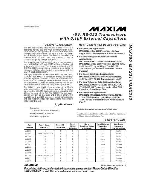
________________________________________________________________Maxim Integrated Products 1General DescriptionThe MAX202E–MAX213E, MAX232E/MAX241E line drivers/receivers are designed for RS-232 and V.28communications in harsh environments. Each transmitter output and receiver input is protected against ±15kV electrostatic discharge (ESD) shocks, without latchup.The various combinations of features are outlined in the Selector Guide.The drivers and receivers for all ten devices meet all EIA/TIA-232E and CCITT V.28specifications at data rates up to 120kbps, when loaded in accordance with the EIA/TIA-232E specification.The MAX211E/MAX213E/MAX241E are available in 28-pin SO packages, as well as a 28-pin SSOP that uses 60% less board space. The MAX202E/MAX232E come in 16-pin TSSOP, narrow SO, wide SO, and DIP packages. The MAX203E comes in a 20-pin DIP/SO package, and needs no external charge-pump capacitors. The MAX205E comes in a 24-pin wide DIP package, and also eliminates external charge-pump capacitors. The MAX206E/MAX207E/MAX208E come in 24-pin SO, SSOP, and narrow DIP packages. The MAX232E/MAX241E operate with four 1µF capacitors,while the MAX202E/MAX206E/MAX207E/MAX208E/MAX211E/MAX213E operate with four 0.1µF capacitors,further reducing cost and board space.________________________ApplicationsNotebook, Subnotebook, and Palmtop Computers Battery-Powered Equipment Hand-Held EquipmentNext-Generation Device Featureso For Low-Voltage ApplicationsMAX3222E/MAX3232E/MAX3237E/MAX3241E/MAX3246E: ±15kV ESD-Protected Down to10nA, +3.0V to +5.5V, Up to 1Mbps, True RS-232Transceivers (MAX3246E Available in a UCSP™Package)o For Low-Power ApplicationsMAX3221/MAX3223/MAX3243: 1µA SupplyCurrent, True +3V to +5.5V RS-232 Transceivers with Auto-Shutdown™o For Space-Constrained ApplicationsMAX3233E/MAX3235E: ±15kV ESD-Protected,1µA, 250kbps, +3.0V/+5.5V, Dual RS-232Transceivers with Internal Capacitorso For Low-Voltage or Data Cable ApplicationsMAX3380E/MAX3381E: +2.35V to +5.5V, 1µA,2Tx/2Rx RS-232 Transceivers with ±15kV ESD-Protected I/O and Logic PinsMAX202E–MAX213E, MAX232E/MAX241E±15kV ESD-Protected, +5V RS-232 TransceiversSelector Guide19-0175; Rev 6; 3/05Pin Configurations and Typical Operating Circuits appear at end of data sheet.YesPARTNO. OF RS-232DRIVERSNO. OF RS-232RECEIVERSRECEIVERS ACTIVE IN SHUTDOWNNO. OF EXTERNAL CAPACITORS(µF)LOW-POWER SHUTDOWNTTL TRI-STATE MAX202E 220 4 (0.1)No No MAX203E 220None No No MAX205E 550None Yes Yes MAX206E 430 4 (0.1)Yes Yes MAX207E 530 4 (0.1)No No MAX208E 440 4 (0.1)No No MAX211E 450 4 (0.1)Yes Yes MAX213E 452 4 (0.1)Yes Yes MAX232E 220 4 (1)No No MAX241E454 (1)YesFor pricing, delivery, and ordering information,please contact Maxim/Dallas Direct!at 1-888-629-4642, or visit Maxim’s website at .AutoShutdown and UCSP are trademarks of Maxim Integrated Products, Inc.Ordering InformationOrdering Information continued at end of data sheet.2_______________________________________________________________________________________M A X 202E –M A X 213E , M A X 232E /M A X 241EABSOLUTE MAXIMUM RATINGSV CC ..........................................................................-0.3V to +6V V+................................................................(V CC - 0.3V) to +14V V-............................................................................-14V to +0.3V Input VoltagesT_IN............................................................-0.3V to (V+ + 0.3V)R_IN...................................................................................±30V Output VoltagesT_OUT.................................................(V- - 0.3V) to (V+ + 0.3V)R_OUT......................................................-0.3V to (V CC + 0.3V)Short-Circuit Duration, T_OUT....................................Continuous Continuous Power Dissipation (T A = +70°C)16-Pin Plastic DIP (derate 10.53mW/°C above +70°C)....842mW 16-Pin Narrow SO (derate 8.70mW/°C above +70°C).....696mW 16-Pin Wide SO (derate 9.52mW/°C above +70°C)......762mW 16-Pin TSSOP (derate 9.4mW/°C above +70°C)...........755mW20-Pin Plastic DIP (derate 11.11mW/°C above +70°C)...889mW 20-Pin SO (derate 10.00mW/°C above +70°C).............800mW 24-Pin Narrow Plastic DIP(derate 13.33mW/°C above +70°C) ...............................1.07W 24-Pin Wide Plastic DIP(derate 14.29mW/°C above +70°C)................................1.14W 24-Pin SO (derate 11.76mW/°C above +70°C).............941mW 24-Pin SSOP (derate 8.00mW/°C above +70°C)..........640mW 28-Pin SO (derate 12.50mW/°C above +70°C)....................1W 28-Pin SSOP (derate 9.52mW/°C above +70°C)..........762mW Operating Temperature RangesMAX2_ _EC_ _.....................................................0°C to +70°C MAX2_ _EE_ _...................................................-40°C to +85°C Storage Temperature Range.............................-65°C to +165°C Lead Temperature (soldering, 10s).................................+300°CELECTRICAL CHARACTERISTICS(V CC = +5V ±10% for MAX202E/206E/208E/211E/213E/232E/241E; V CC = +5V ±5% for MAX203E/205E/207E; C1–C4 = 0.1µF for MAX202E/206E/207E/208E/211E/213E; C1–C4 = 1µF for MAX232E/241E; T A = T MIN to T MAX ; unless otherwise noted. Typical values are at T A = +25°C.)Stresses beyond those listed under “Absolute Maximum Ratings” may cause permanent damage to the device. These are stress ratings only, and functional operation of the device at these or any other conditions beyond those indicated in the operational sections of the specifications is not implied. Exposure to absolute maximum rating conditions for extended periods may affect device reliability.ELECTRICAL CHARACTERISTICS (continued)MAX202E–MAX213E, MAX232E/MAX241E (V CC= +5V ±10% for MAX202E/206E/208E/211E/213E/232E/241E; V CC= +5V ±5% for MAX203E/205E/207E; C1–C4 = 0.1µF forMAX202E/206E/207E/208E/211E/213E; C1–C4 = 1µF for MAX232E/241E; T A= T MIN to T MAX; unless otherwise noted. Typical valuesare at T A= +25°C.)Note 1:MAX211EE_ _ tested with V CC= +5V ±5%._______________________________________________________________________________________34______________________________________________________________________________________M A X 202E –M A X 213E , M A X 232E /M A X 241E__________________________________________Typical Operating Characteristics(Typical Operating Circuits, V CC = +5V, T A = +25°C, unless otherwise noted.)5.00MAX211E/MAX213ETRANSMITTER OUTPUT VOLTAGEvs. LOAD CAPACITANCELOAD CAPACITANCE (pF)V O H , -V O L (V )5.56.06.57.07.58.0100020003000400050000MAX211E/MAX213E/MAX241E TRANSMITTER SLEW RATE vs. LOAD CAPACITANCELOAD CAPACITANCE (pF)S L E W R A T E ( V /µs )5101520253010002000300040005000_______________________________________________________________________________________5MAX202E–MAX213E, MAX232E/MAX241E____________________________Typical Operating Characteristics (continued)(Typical Operating Circuits, V CC = +5V, T A = +25°C, unless otherwise noted.)2MAX202E/MAX203E/MAX232E TRANSMITTER SLEW RATE vs. LOAD CAPACITANCELOAD CAPACITANCE (pF)S L E W R A T E ( V /µs )468101214100020003000400050005.07.5-7.53000MAX205E–MAX208ETRANSMITTER OUTPUT VOLTAGEvs. LOAD CAPACITANCE-5.02.5LOAD CAPACITANCE (pF)O U T P U T V O L T A G E (V )10002000400050000-2.54550203000MAX205E–MAX208E SUPPLY CURRENT vs. LOAD CAPACITANCE2540LOAD CAPACITANCE (pF)S U P P L Y C U R R E N T (m A )100020004000500035302.55.0-10.0180MAX205E –MAX208EOUTPUT VOLTAGE vs. DATA RATE-7.50DATA RATE (kbps)O U T P U T V O L T A G E (V )601202401503090210-2.5-5.010.07.56_______________________________________________________________________________________M A X 202E –M A X 213E , M A X 232E /M A X 241EMAX203EMAX205E_____________________________________________________________Pin DescriptionsMAX202E/MAX232E_______________________________________________________________________________________7MAX202E–MAX213E, MAX232E/MAX241EMAX208E________________________________________________Pin Descriptions (continued)MAX206EMAX207E8_______________________________________________________________________________________M A X 202E –M A X 213E , M A X 232E /M A X 241EMAX211E/MAX213E/MAX241E)(MAX205E/MAX206E/MAX211E/MAX213E/MAX241E)________________________________________________Pin Descriptions (continued)MAX211E/MAX213E/MAX241EFigure 3. Transition Slew-Rate Circuit_______________Detailed Description The MAX202E–MAX213E, MAX232E/MAX241E consist of three sections: charge-pump voltage converters, drivers (transmitters), and receivers. These E versions provide extra protection against ESD. They survive ±15kV discharges to the RS-232 inputs and outputs, tested using the Human Body Model. When tested according to IEC1000-4-2, they survive ±8kV contact-discharges and ±15kV air-gap discharges. The rugged E versions are intended for use in harsh environments or applications where the RS-232 connection is frequently changed (such as notebook computers). The standard (non-“E”) MAX202, MAX203, MAX205–MAX208, MAX211, MAX213, MAX232, and MAX241 are recommended for applications where cost is critical.+5V to ±10V Dual Charge-PumpVoltage Converter The +5V to ±10V conversion is performed by dual charge-pump voltage converters (Figure 4). The first charge-pump converter uses capacitor C1 to double the +5V into +10V, storing the +10V on the output filter capacitor, C3. The second uses C2 to invert the +10V into -10V, storing the -10V on the V- output filter capacitor, C4.In shutdown mode, V+ is internally connected to V CC by a 1kΩpull-down resistor, and V- is internally connected to ground by a 1kΩpull up resistor.RS-232 Drivers With V CC= 5V, the typical driver output voltage swing is ±8V when loaded with a nominal 5kΩRS-232 receiver. The output swing is guaranteed to meet EIA/TIA-232E and V.28 specifications that call for ±5V minimum output levels under worst-case conditions. These include a 3kΩload, minimum V CC, and maximum operating temperature. The open-circuit output voltage swings from (V+ - 0.6V) to V-.Input thresholds are CMOS/TTL compatible. The unused drivers’ inputs on the MAX205E–MAX208E, MAX211E, MAX213E, and MAX241E can be left unconnected because 400kΩpull up resistors to V CC are included on-chip. Since all drivers invert, the pull up resistors force the unused drivers’ outputs low. The MAX202E, MAX203E, and MAX232E do not have pull up resistors on the transmitter inputs._______________________________________________________________________________________9MAX202E–MAX213E, MAX232E/MAX241E10______________________________________________________________________________________M A X 202E –M A X 213E , M A X 232E /M A X 241E±15kV ESD-Protected, +5V RS-232 Transceivers When in low-power shutdown mode, the MAX205E/MAX206E/MAX211E/MAX213E/MAX241E driver outputs are turned off and draw only leakage currents—even if they are back-driven with voltages between 0V and 12V. Below -0.5V in shutdown, the transmitter output is diode-clamped to ground with a 1k Ωseries impedance.RS-232 ReceiversThe receivers convert the RS-232 signals to CMOS-logic output levels. The guaranteed 0.8V and 2.4V receiver input thresholds are significantly tighter than the ±3V thresholds required by the EIA/TIA-232E specification.This allows the receiver inputs to respond to TTL/CMOS-logic levels, as well as RS-232 levels.The guaranteed 0.8V input low threshold ensures that receivers shorted to ground have a logic 1 output. The 5k Ωinput resistance to ground ensures that a receiver with its input left open will also have a logic 1 output. Receiver inputs have approximately 0.5V hysteresis.This provides clean output transitions, even with slow rise/fall-time signals with moderate amounts of noise and ringing.In shutdown, the MAX213E’s R4 and R5 receivers have no hysteresis.Shutdown and Enable Control (MAX205E/MAX206E/MAX211E/MAX213E/MAX241E)In shutdown mode, the charge pumps are turned off,V+ is pulled down to V CC , V- is pulled to ground, and the transmitter outputs are disabled. This reduces supply current typically to 1µA (15µA for the MAX213E).The time required to exit shutdown is under 1ms, as shown in Figure 5.ReceiversAll MAX213E receivers, except R4 and R5, are put into a high-impedance state in shutdown mode (see Tables 1a and 1b). The MAX213E’s R4 and R5 receivers still function in shutdown mode. These two awake-in-shutdown receivers can monitor external activity while maintaining minimal power consumption.The enable control is used to put the receiver outputs into a high-impedance state, to allow wire-OR connection of two EIA/TIA-232E ports (or ports of different types) at the UART. It has no effect on the RS-232 drivers or the charge pumps.N ote: The enabl e control pin is active l ow for the MAX211E/MAX241E (EN ), but is active high for the MAX213E (EN). The shutdown control pin is active high for the MAX205E/MAX206E/MAX211E/MAX241E (SHDN), but is active low for the MAX213E (SHDN ).Figure 4. Charge-Pump DiagramMAX202E–MAX213E, MAX232E/MAX241EV+V-200µs/div3V 0V 10V 5V 0V -5V -10VSHDNMAX211EFigure 5. MAX211E V+ and V- when Exiting Shutdown (0.1µF capacitors)X = Don't care.*Active = active with reduced performanceSHDN E N OPERATION STATUS Tx Rx 00Normal Operation All Active All Active 01Normal Operation All Active All High-Z 1XShutdownAll High-ZAll High-ZTable 1a. MAX205E/MAX206E/MAX211E/MAX241E Control Pin ConfigurationsTable 1b. MAX213E Control Pin ConfigurationsThe MAX213E’s receiver propagation delay is typically 0.5µs in normal operation. In shutdown mode,propagation delay increases to 4µs for both rising and falling transitions. The MAX213E’s receiver inputs have approximately 0.5V hysteresis, except in shutdown,when receivers R4 and R5 have no hysteresis.When entering shutdown with receivers active, R4 and R5 are not valid until 80µs after SHDN is driven low.When coming out of shutdown, all receiver outputs are invalid until the charge pumps reach nominal voltage levels (less than 2ms when using 0.1µF capacitors).±15kV ESD ProtectionAs with all Maxim devices, ESD-protection structures are incorporated on all pins to protect against electrostatic discharges encountered during handling and assembly. The driver outputs and receiver inputs have extra protection against static electricity. Maxim’s engineers developed state-of-the-art structures to protect these pins against ESD of ±15kV without damage. The ESD structures withstand high ESD in all states: normal operation, shutdown, and powered down. After an ESD event, Maxim’s E versions keep working without latchup, whereas competing RS-232products can latch and must be powered down to remove latchup.ESD protection can be tested in various ways; the transmitter outputs and receiver inputs of this product family are characterized for protection to the following limits:1)±15kV using the Human Body Model2)±8kV using the contact-discharge method specifiedin IEC1000-4-23)±15kV using IEC1000-4-2’s air-gap method.ESD Test ConditionsESD performance depends on a variety of conditions.Contact Maxim for a reliability report that documents test set-up, test methodology, and test results.Human Body ModelFigure 6a shows the Human Body Model, and Figure 6b shows the current waveform it generates when discharged into a low impedance. This model consists of a 100pF capacitor charged to the ESD voltage of interest, which is then discharged into the test device through a 1.5k Ωresistor.S H D N ENOPERATION STATUS Tx 1–400Shutdown All High-Z 01Shutdown All High-Z 10Normal Operation 11Normal OperationAll ActiveAll Active Active1–34, 5High-Z ActiveHigh-Z High-Z High-Z Active*High-Z RxM A X 202E –M A X 213E , M A X 232E /M A X 241EIEC1000-4-2The IEC1000-4-2 standard covers ESD testing and performance of finished equipment; it does not specifically refer to integrated circuits. The MAX202E/MAX203E–MAX213E, MAX232E/MAX241E help you design equipment that meets level 4 (the highest level) of IEC1000-4-2, without the need for additional ESD-protection components.The major difference between tests done using the Human Body Model and IEC1000-4-2 is higher peak current in IEC1000-4-2, because series resistance is lower in the IEC1000-4-2 model. Hence, the ESD withstand voltage measured to IEC1000-4-2 is generally lower than that measured using the Human Body Model. Figure 7b shows the current waveform for the 8kV IEC1000-4-2 level-four ESD contact-discharge test.The air-gap test involves approaching the device with a charged probe. The contact-discharge method connects the probe to the device before the probe is energized.Machine ModelThe Machine Model for ESD tests all pins using a 200pF storage capacitor and zero discharge resistance. Its objective is to emulate the stress caused by contact that occurs with handling and assembly during manufacturing. Of course, all pins require this protection during manufacturing, not just RS-232 inputs and outputs. Therefore,after PC board assembly,theMachine Model is less relevant to I/O ports.Figure 7a. IEC1000-4-2 ESD Test ModelFigure 7b. IEC1000-4-2 ESD Generator Current WaveformFigure 6a. Human Body ESD Test ModelFigure 6b. Human Body Model Current Waveform__________Applications InformationCapacitor Selection The capacitor type used for C1–C4 is not critical for proper operation. The MAX202E, MAX206–MAX208E, MAX211E, and MAX213E require 0.1µF capacitors, and the MAX232E and MAX241E require 1µF capacitors, although in all cases capacitors up to 10µF can be used without harm. Ceramic, aluminum-electrolytic, or tantalum capacitors are suggested for the 1µF capacitors, and ceramic dielectrics are suggested for the 0.1µF capacitors. When using the minimum recommended capacitor values, make sure the capacitance value does not degrade excessively as the operating temperature varies. If in doubt, use capacitors with a larger (e.g., 2x) nominal value. The capacitors’ effective series resistance (ESR), which usually rises at low temperatures, influences the amount of ripple on V+ and V-.Use larger capacitors (up to 10µF) to reduce the output impedance at V+ and V-. This can be useful when “stealing” power from V+ or from V-. The MAX203E and MAX205E have internal charge-pump capacitors. Bypass V CC to ground with at least 0.1µF. In applications sensitive to power-supply noise generated by the charge pumps, decouple V CC to ground with a capacitor the same size as (or larger than) the charge-pump capacitors (C1–C4).V+ and V- as Power Supplies A small amount of power can be drawn from V+ and V-, although this will reduce both driver output swing and noise margins. Increasing the value of the charge-pump capacitors (up to 10µF) helps maintain performance when power is drawn from V+ or V-.Driving Multiple Receivers Each transmitter is designed to drive a single receiver. Transmitters can be paralleled to drive multiple receivers.Driver Outputs when Exiting Shutdown The driver outputs display no ringing or undesirable transients as they come out of shutdown.High Data Rates These transceivers maintain the RS-232 ±5.0V minimum driver output voltages at data rates of over 120kbps. For data rates above 120kbps, refer to the Transmitter Output Voltage vs. Load Capacitance graphs in the Typical Operating Characteristics. Communication at these high rates is easier if the capacitive loads on the transmitters are small; i.e., short cables are best.Table 2. Summary of EIA/TIA-232E, V.28 SpecificationsMAX202E–MAX213E, MAX232E/MAX241EM A X 202E –M A X 213E , M A X 232E /M A X 241E____________Pin Configurations and Typical Operating Circuits (continued)Table 3. DB9 Cable ConnectionsCommonly Used for EIA/TIAE-232E and V.24 Asynchronous Interfaces____________Pin Configurations and Typical Operating Circuits (continued)MAX202E–MAX213E, MAX232E/MAX241EM A X 202E –M A X 213E , M A X 232E /M A X 241E____________Pin Configurations and Typical Operating Circuits (continued)MAX202E–MAX213E, MAX232E/MAX241E____________Pin Configurations and Typical Operating Circuits (continued)M A X 202E –M A X 213E , M A X 232E /M A X 241E____________Pin Configurations and Typical Operating Circuits (continued)MAX202E–MAX213E, MAX232E/MAX241E____________Pin Configurations and Typical Operating Circuits (continued)M A X 202E –M A X 213E , M A X 232E /M A X 241E____________Pin Configurations and Typical Operating Circuits (continued)______________________________________________________________________________________21MAX202E–MAX213E, MAX232E/MAX241E Ordering Information (continued)*Dice are specified at T A= +25°C.M A X 202E –M A X 213E , M A X 232E /M A X 241E22________________________________________________________________________________________________________________________________________________Chip Topographies___________________Chip InformationC1-V+C1+V CC R2INT2OUT R2OUT0.117"(2.972mm)0.080"(2.032mm)V-C2+ C2-T2IN T1OUT R1INR1OUT T1INGNDR5INV-C2-C2+C1-V+C1+V CC T4OUTR3IN T3OUTT1OUT 0.174"(4.420mm)0.188"(4.775mm)T4IN R5OUT R4OUT T3IN R4IN EN (EN) SHDN (SHDN)R3OUT T2OUT GNDR1IN R1OUT T2IN R2OUTR2IN T1IN ( ) ARE FOR MAX213E ONLYTRANSISTOR COUNT: 123SUBSTRATE CONNECTED TO GNDTRANSISTOR COUNT: 542SUBSTRATE CONNECTED TO GNDMAX202E/MAX232EMAX211E/MAX213E/MAX241EMAX205E/MAX206E/MAX207E/MAX208E TRANSISTOR COUNT: 328SUBSTRATE CONNECTED TO GNDMAX202E–MAX213E, MAX232E/MAX241E Package InformationM A X 202E –M A X 213E , M A X 232E /M A X 241EPackage Information (continued)MAX202E–MAX213E, MAX232E/MAX241E±15kV ESD-Protected, +5V RS-232 TransceiversMaxim cannot assume responsibility for use of any circuitry other than circuitry entirely embodied in a Maxim product. No circuit patent licenses are implied. Maxim reserves the right to change the circuitry and specifications without notice at any time.Maxim Integrated Products, 120 San Gabriel Drive, Sunnyvale, CA 94086 408-737-7600 ____________________25©2005 Maxim Integrated ProductsPrinted USAis a registered trademark of Maxim Integrated Products, Inc.Package Information (continued)(The package drawing(s) in this data sheet may not reflect the most current specifications. For the latest package outline information go to /packages .)。

General DescriptionThe MAX4211E evaluation kit (EV kit) is a fully assembled and tested surface-mount circuit board that provides overpower circuit-breaker and fault protection using the MAX4211E power-monitoring IC. The EV kit demonstrates the programmable overpower monitoring feature with manual or microcontroller reset options of the MAX4211E.The MAX4211E controls an external p-channel high-side power MOSFET to provide overpower fault protection.The MAX4211E EV kit’s circuit overpower threshold is configured for 100W with a maximum input voltage of 20V and up to 5A of load current. This makes it suitable for circuit-breaker applications in notebooks and other portable power systems. The EV kit may be reconfig-ured for other power thresholds with a maximum load current of up to 10A.The EV kit can also be used to evaluate other versions of the MAX4211 power-monitoring ICs.Featureso Configured for 100W Overpower Threshold o Configured for 5V to 20V Maximum Input Voltage o Configured for 5A Load-Current Threshold o Reconfigurable Overpower Thresholds o Immune to Power-Up Capacitive Load Spikes o Configurable Reset (Manual or Microcontroller)o Surface-Mount Components o Fully Assembled and Testedo Evaluates MAX4211A, MAX4211B, MAX4211C,MAX4211D, or MAX4211F (IC Replacement Required)Evaluates: MAX4211A/B/C/D/E/FMAX4211E Evaluation Kit________________________________________________________________Maxim Integrated Products 119-3399; Rev 1; 3/05For pricing, delivery, and ordering information,please contact Maxim/Dallas Direct!at 1-888-629-4642, or visit Maxim’s website at .Ordering InformationComponent ListE v a l u a t e s : M A X 4211A /B /C /D /E /FQuick StartThe MAX4211E EV kit is fully assembled and tested.Follow these steps to verify board operation. Do not turn on the power supply until all connections are completed.Recommended Equipment•0 to 20V power supply capable of providing up to 5A •5V power supply•Electronic load capable of sinking up to 5A (e.g.,HP 6060B)Procedures1)Verify that a shunt is installed across pins 2 and 3 ofjumper JU1.2)Verify that shunts are installed on jumpers J U2and JU3.3)Set the 0 to 20V power supply to 10V and disablethe output.4)Connect the positive terminal of the 0 to 20V DCpower supply to the VSOURCE pad on the EV kit board. Connect the ground of this power supply to the GND pad located above the VSOURCE pads.5)Connect a voltmeter across the VSOURCE andGND pads.6)Connect the positive terminal of the 5A DC electroniccurrent load to the LOAD pad on the EV kit board.Connect the ground terminal of the electronic load to the GND pad located above the LOAD pad on the EV kit.7)Connect the positive terminal of the 5V DC powersupply to the VCC pad. Connect the ground of this power supply to the GND pad located below the VCC pad on the EV kit board.8)Connect a voltmeter across the LOAD and GNDpads on the EV kit board.9)Connect a voltmeter across the TP2 test point andGND pad.10)Turn on the 5V power supply.11)Enable the 0 to 20V (10V) power supply.12)Turn on the electronic current load.13)Verify that the voltmeter connected across theLOAD and GND pads measures 10V.14)Verify that the voltmeter connected at test point TP2measures approximately 1.25V.15)Gradually increase the VSOURCE power supplytowards 20V to cause an overpower fault,16)After the fault, verify that the voltmeter connectedacross the LOAD and GND pads measures 0V.17)Verify that the voltmeter connected at TP2 mea-sures 0V.18)Reduce V SOURCE to 10V and then reset the circuit bymomentarily pressing pushbutton SW1. Verify that the voltmeter connected at TP2 measures approximately 1.25V and LOAD voltage returns to 10V.Detailed DescriptionThe MAX4211E EV kit is a power-monitoring, circuit-breaker circuit that safeguards the supply source against excessive power dissipation due to overvoltage,overcurrent, or short-circuit conditions at the output. The circuit uses the MAX4211E power-monitoring IC that operates with a V CC voltage range of 2.7V to 5.5V.MAX4211E Evaluation Kit 2_______________________________________________________________________________________The load can be supplied through an independent sup-ply source connected across the VSOURCE and GND pads and can range from 5V to 20V. The MAX4211E controls an external high-side p-channel power MOSFET switch that disconnects the supply source from the load under overpower fault conditions.During normal operation, the EV kit circuit continually monitors the power delivered to the load. When the power delivered to the load exceeds the configured maximum power threshold, the circuit disconnects the supply source from the load thus providing overpower fault pro-tection. The EV kit can be reset to normal operation by first removing the fault condition and then momentarily pressing pushbutton SW1. The EV kit is configured for a power threshold of 100W with an input source voltage threshold of 20V and load-current threshold of 5A. The MAX4211E EV kit can be reconfigured to monitor up to 10A of current.Input Voltages The MAX4211E EV kit provides the flexibility of having independent power-supply sources for the IC and the load. The EV kit is configured for a maximum V SOURCE of 20V and a V CC of 5V. To reconfigure the EV kit’s V SOURCE maximum input voltage for up to 28V, see the Overpower Threshold section. Set the V CC voltage in the range of 2.7V to 5.5V.Overpower Threshold The overpower threshold for the MAX4211E EV kit is set to 100W with a maximum V SOURCE input voltage of 20V and maximum load current of 5A. During normal opera-tion, the EV kit circuit continually monitors the power delivered to the load. When the power delivered to the load exceeds the 100W threshold (after exceeding the 20V and 5A thresholds), the MAX4211E disconnects the supply source from the load. This is done by switching MOSFET P1 off when the MAX4211E COUT1 pin latches high.To reconfigure the MAX4211E EV kit for a different overpower threshold, the V SOURCE and load-current thresholds must be modified. Reconfigure the V SOURCE voltage threshold for up to 28V by selecting new resis-tor values for R2 and R3 using the following equation: R2 = R3 x (V SOURCE_THRESHOLD- 1)where resistor R3 is typically 6.98kΩand the V SOURCE_THRESHOLD is the new desired value. This step ensures that the MAX4211E POUT pin is 2.5V when the maximum power is delivered to the load.The MAX4211E EV kit board is configured for a load-current threshold of 5A DC, however, the 2oz PC board traces can handle up to 10A. Use the following equa-tion to select a new value for current-sense resistor R1 (2512 case):Verify that the resistor R1 and MOSFET P1 are rated for the new current level.Reset During an overpower fault condition, the MAX4211E EV kit circuit latches off. To reset the circuit, remove the fault condition and momentarily press the pushbutton switch SW1. This clears the latched COUT1 pin on the MAX4211E.The MAX4211E EV kit circuit reset function can also be controlled by connecting a microcontroller’s output across the CIN2- and GND pads and configuring jumpers J U1, J U2, and J U3. See Table1 for jumperconfiguration. Evaluates: MAX4211A/B/C/D/E/F MAX4211E Evaluation KitE v a l u a t e s : M A X 4211A /B /C /D /E /FInternal ComparatorsThe MAX4211E features two internal comparators. In the EV kit, circuit Comparator1 is used to detect over-power conditions. Comparator2 is disabled but can be configured for microcontroller reset or other comparator applications. To access CIN2+ of Comparator2,remove the shunt across J U3 and connect to pin 2 of J U3. To access CIN2-, remove the shunt across J U2and connect to the CIN2- pad. The Comparator2 output can be accessed through pin 1 of JU1. CIN2+ can be left connected to REF through JU3 or can be accessed directly through pin 2 of jumper JU3.Power-UpTransient surges in power may result when the EV kit is powered up with a capacitive load connected to the out-put (either C5 on the MAX4211E EV kit or to the LOAD PC board pad output). These transient conditions may be detected as an overpower condition and prevent MOSFET P1 from turning on. Though these transients might not always be sufficient to trip the circuit-breaker function, the MAX4211E possesses an INHIBIT circuit,which can prevent such transients from being registered as overpower conditions.The MAX4211E EV kit features an RC network consist-ing of resistors R6 and capacitor C7 that connects the LOAD node to INHIBIT of the MAX4211E. During power-up, this RC network disables the internal com-parator providing immunity against transient events for a period given by the equation:where ∆V is the voltage change at the LOAD during power-up or due to switching between different voltage sources.The MAX4211E EV kit comes configured with t INHIBIT approximately equal to 425µs, for an expected ∆V =10V and a LOAD voltage settling time of 42.5µs. For some applications, this value might be too short to sus-pend the Comparator1 operation as power-up tran-sients could be much slower. To adjust the inhibit time,select a value of t INHIBIT that is larger than the settling time (t LOAD ) of the LOAD voltage. Selecting t INHIBIT =10 x t LOAD , where t LOAD is the time constant of rising voltage at V LOAD during power-up, is a good design criterion. Larger t INHIBIT times will reduce the number of false circuit-breaker trips, but can potentially subject V SOURCE to longer periods of exposure to momentary overpower conditions.Also note that resistor R7 is merely an isolation resistor with a value that does not affect t INHIBIT.Evaluating the MAX4211A/B/C/D/FThe MAX4211E EV kit can also evaluate other versions of the MAX4211 power-monitoring IC. The MAX4211E IC must be removed and replaced with the desired IC.Refer to the MAX4210/MAX4211 IC data sheet for detailed information about the MAX4211 parts.Depending upon your version of the MAX4211, some ofthe external components may need replacement.MAX4211E Evaluation Kit 4_______________________________________________________________________________________Evaluates: MAX4211A/B/C/D/E/F MAX4211E Evaluation Kit Figure 1. MAX4211E EV Kit Schematic_______________________________________________________________________________________5Maxim cannot assume responsib ility for use of any circuitry other than circuitry entirely emb odied in a Maxim product. No circuit patent licenses are implied. Maxim reserves the right to change the circuitry and specifications without notice at any time.6_____________________Maxim Integrated Products, 120 San Gabriel Drive, Sunnyvale, CA 94086 408-737-7600©2005 Maxim Integrated ProductsPrinted USAis a registered trademark of Maxim Integrated Products, Inc.E v a l u a t e s : M A X 4211A /B /C /D /E /FMAX4211E Evaluation Kit Figure 2. MAX4211E EV Kit Component Placement Guide—Component Side Figure 3. MAX4211E EV Kit PC Board Layout—ComponentSideFigure 4. MAX4211E EV Kit PC Board Layout—Solder Side。


CA1N4867en Siemens Building Technologies4867Two-port and three-portzone valves PN16M..I421..Zone valve for the control of hot or chilled water for • Fan coil units • Induction units• Zones with radiators• Floor heating via manifolds • VAV applications • Wall mounted boilersUse• In ventilation and air conditioning systems for water-side terminal unit control in closed circuits, e.g. induction units, fan coil units, small re-heaters and small re-coolers, for use in:− Two-pipe systems with one heat exchanger for heating and cooling− Four-pipe systems with two separate heat exchangers for heating and cooling • In closed circuit zone heating systems, e.g.− Individual storeys in a building − Apartments−Individual roomsThree-port valves (3-ports)Two-port valves (2-ports)2/8______________________________________________________________________________________________• Hot water:max. 110 °C • Chilled water :above 2 °C • Water containing anti-freeze agents:max. 50 % vol.Water should be treated as specified in VDI 2035Max. 1600 kPa (16 bar) in accordance with ISO 7268 (DIN 2401)Type summaryDN Connectionk vsM..I.421...(2 ports)∆p s MXI...421...(3 ports)∆p max 1)Actuator Positioning force [mm][m 3/h][kPa][kPa]15R P ½“ 2.0MVI421.15300MXI421.1515020R P ¾“ 3.5MVI421.20300MXI421.2025R P 1“5.0MVI421.25150MXI421.25105N1) For ∆p max =Where ∆p max is above 150 kPa, there is an increased risk of noise and erosionon the seat and plug ∆p s =Max. admissible pressure differential in kPa at which the valve is still capable of closing against the pressure∆p max=Max. admissible pressure differential across the closed valve/actuator assemblyTyp DesignationSwitching point Contact rating ASC2.1Auxiliary switch on / offwith approx. 50 % strokeAC 250 V / 1 AOrderingWhen ordering, please specify the quantity, product name and type reference10 three-port valve, type MXI421.25The valves and actuators are packed together.FunctionThe zone valves are closed when de-energised. An on/off controller (thermostat) is required to drive the motorised valve actuators. If the temperature of the medium deviates from the setpoint, the controller delivers a control signal which drives theactuators, causing the valve to open. When the temperature of the medium reaches the setpoint, the control signal is cut off and the valve closes.If required the MVI421…/MXI421… the valve can be added with an auxiliary switch ASC2.1.MediaRecommendation Operating pressureAsscessoriesExampleDelivery3/8Engineering notesThe valves should preferably be installed in the return, where the seals are exposed to lower temperatures. See also «Mounting notes» and «Commissioning notes».A strainer should be fitted upstream of the valve.Port AB =Variable flow through straight-through port (inlet)Port A =Variable flow through straight-through port (outlet)Stem retracted:Path AB → A closed Stem extended:Path AB → A openPort AB =Constant total flow (inlet)Port A =Variable flow AB → A (outlet A)Port B =Variable flow AB → B through bypass (outlet B)Stem retracted:Path AB → A closed, bypass B open Stem extended:Path A → AB open, bypass B closedRecommendation:Two-port valves (2 ports)MVI421…Three-port valves (3 ports)MXI421Flow only permissible in direction of arrow from AB →A (marked on valve body).MXI421.. are diverting valves they can be used under certain circumstances as mixing valves (see «Use as mixing valves»).Diverting mode:Flow from AB → A and B4/8MXI421… are diverting valves . Under consideration of certain conditions they can be used as mixing valves too:Mounting in the return pipeAllowable ∆p v max in relation to the system pressure∆p m a x [b a r ]123456789System pressure [bar]At a system pressure of 5.5 bar (550 kPa) the maximum differential pressure ∆p v max shoult not exceed 0.4bar (40 kPa).Mounting notesPermissible Not permissibleIn addition, the direction of flow as described under «Engineering notes» must be e as mixing valvesExampleCaution:Suitable conduit shall connected to the actuator when undergon the wiring work of the product.5/8Manual OperationValve manually openTurning switch with approximately 90 % valve strokelatchSwitch manually releaseCommissioning notes Through operation of the manual adjuster or removed the actuator, the trough-port AB → A of the valve can be opened. With the 3 port valves, the bypass port will be closed.The valves will be opened by their own spring (normally open).Before performing any service work on the valve and/or actuator: switch OFF the pump and power supply, close the main shut-off valve in the pipework, release pressure in the pipes and allow them to cool down completely. If necessary, disconnect electrical connections from the terminals. The valve may be commissioned only with the manual wheel pre-set or with a correctly mounted actuator.MaintenanceThe valve and actuator do not require maintenanceFaulty actuators can be replaced without removing the valve from the pipework.The actuator cannot be repaired.Replacement actuators (AC 230 V versions)can be ordered by quoting type code :SFA21AC 24V versions can be ordered by quoting type code : SFA71Manual adjustmentWarning !Replacement actuatorTechnical dataOperating data Operating Pressure PN16Leakage–Path AB → A –Bypass B 0 … 0.05 % of k vs max. 5 % of k vsPressure class PN16Acc. to ISO 7268 (DIN 2401)Nominal stroke 2.5 mmMaterials Valve materials–Valve body– Stem–Plug, seat, gland –O-rings BrassStainless steelBrass or bronze Rg5 Special EPDM rubberDimensions / Weights Dimensions see «Dimensions» (table)Threaded connections–Valve BS 21 / ISO7-1Weights see «Dimensions» (table) AccessoriesPower Supply Operating VoltageFrequencyPower Consumption 230VAC – 15 / +10% 50/60Hz9.8 VAFunction Running timeNominal strokeNominal force 35 seconds 2.5 mm 105NGeneral ambient conditions OperationTemperature Humidity 1 to 110o C5 to 85% rh (non-condensing)Storage / transportTemperature Humidity -25 to 70o C95% rh (non-condensing)CE confirmity Meets the requirement for CE confirmityto- EMC Directive-Low voltage Directive 89/336/EEC 73/23/EECConnection DiagramValves MVI421.. and MXI421…without auxiliary switch Valves MVI421.. and MXI421…Withauxiliary switchY1Zone valve with actuatorc1Auxiliary switch (N/O contact)N1Temperature controller (thermostat)⊥Earthing conductor (yellow/green)N Neutral conductor (blue)L Phase (brown)3Auxiliary switch (orange)4Auxiliary switch (grey)6/87/8Dimensions All dimensions in mmDN Thread Valve type D H H3L1L2G [mm][kg]15Rp½“MVI421.153526011060300.86520Rp¾“MVI421.20352601106532.50.89525Rp1“MVI421.25352601108442 1.105DN Thread Valve typeD H H3L1L2L3G [mm][kg]15Rp½“MXI421.15302601106030300.93420Rp¾“MXI421.20352601106532.532.50.96525Rp1“MXI421.2535260110844240 1.215Two-port valves (2 ports)MVI421…Three-port valves (3 ports)MXI421…8/8 2001 Siemens Building Technologies Ltd.Subject to changes。


IVSEVINMP421EVAL-ADMP421Z-FLEXOmnidirectional Microphone with Bottom Port and Digital OutputData SheetADMP421Rev. DInformation furnished by Analog Devices is believed to be accurate and reliable. However , no responsibility is assumed by Analog Devices for its use, nor for any infringements of patents or other rights of third parties that may result from its use. Specifications subject to change without notice. No license is granted by implication or otherwise under any patent or patent rights of Analog Devices. T rademarks and registered trademarks are the property of their respective owners.One Technology Way, P.O. Box 9106, N orwood, MA 02062-9106, U.S.A. Tel: 781.329.4700 Fax: 781.461.3113 ©2010–2011 Analog Devices, Inc. All rights reserved.FEATURESSmall and thin 3 mm × 4 mm × 1 mm surface-mount package High SNR of 61 dBAHigh sensitivity of −26 dBFSFlat frequency response from 100 Hz to 15 kHz Low current consumption: <650 µA Sleep mode for extended battery life High PSR of 80 dBFSFourth-order Σ-Δ modulator Digital PDM outputCompatible with Sn/Pb and Pb-free solder processes RoHS/WEEE compliantAPPLICATIONSSmartphones and feature phones Teleconferencing systems Digital video cameras Bluetooth headsets Video phones TabletsGENERAL DESCRIPTIONThe ADMP421 is a high performance, low power, digital output bottom-ported omnidirectional MEMS microphone. The ADMP421 consists of a MEMS microphone element and an impedance converter amplifier followed by a fourth-order Σ-Δ modulator. The digital interface allows for the pulse density modulated (PDM) output of two microphones to be time-multiplexed on a single data line using a single clock.The ADMP421 has a high SNR and high sensitivity, making it an excellent choice for far field applications. The ADMP421 has a flat wideband frequency response, resulting in natural sound with high intelligibility. Low current consumption and a sleep mode enable long battery life for portable applications. A built-in particle filter provides high reliability. The ADMP421 complies with the TIA-920 Telecommunications Telephone Terminal Equipment Transmission Requirements for Wideband Digital Wireline Telephones standard.The ADMP421 is available in a thin 3 mm × 4 mm × 1 mm surface-mount package. It is reflow solder compatible with no sensitivity degradation. The ADMP421 is halide free.FUNCTIONAL BLOCK DIAGRAMV D DG N DL /R S E L E C T07596-001Figure 1.OB L E T EADMP421Data SheetRev. D | Page 2 of 16TABLE OF CONTENTSFeatures .............................................................................................. 1 Applications ....................................................................................... 1 General Description ......................................................................... 1 Functional Block Diagram .............................................................. 1 Revision History ............................................................................... 2 Specifications ..................................................................................... 3 Timing Characteristics ................................................................ 4 Absolute Maximum Ratings ............................................................ 5 ESD Caution .................................................................................. 5 Pin Configuration and Function Descriptions ............................. 6 Typical Performance Characteristics ............................................. 7 PCB Land Pattern Layout ................................................................ 8 Alternate PCB Land Patterns ...................................................... 9 Applications Information .............................................................. 10 Interfacing with Analog Devices Codecs ................................ 10 Sleep Mode .................................................................................. 10 Power Savings When Disabling One Microphone in aMultimicrophone Application .................................................. 10 Supporting Documents ............................................................. 10 Handling Instructions .................................................................... 11 Pick-and-Place Equipment ....................................................... 11 Reflow Solder .............................................................................. 11 Board Wash ................................................................................. 11 Reliability Specifications ................................................................ 12 Outline Dimensions ....................................................................... 13 Ordering Guide .. (13)REVISION HISTORY11/11—Rev. C to Rev. DChanged PSRR to PSR ....................................................... U niversal Changed Pb-Free Temperature from 245°C to 260°C, Table 4 .. 5 Changes to Figure 8 and Figure 9 ................................................... 8 Added Alternate PCB Land Patterns Section ............................... 9 Changes to Temperature Humidity Bias (THB) Description, Table 6 . (12)8/11—Rev. B to Rev. CChanges to Clock Frequency and Supply Voltage Parameters, Table 1 ................................................................................................ 3 Changes to Table 3 and Table 4 ....................................................... 5 Deleted Power-Saving Features Section ........................................ 8 Changes to Figure 9 .......................................................................... 8 Added Applications Information Section ..................................... 9 Added Supporting Documents, Evaluation Board User Guides, Circuit Note, and Application Notes Sections .............................. 9 Changes to Interfacing with Analog Devices CodecsSection ................................................................................................ 9 Moved Sleep Mode Section and Power Savings When Disabling One Microphone in a Multimicrophone Application Section ... 9 Changes to Figure 10 ........................................................................ 9 Change to Pick-and-Place Equipment Section ........................... 10 Deleted Evaluation Board Section ................................................ 10 Deleted Figure 10 and Figure 11; Renumbered Sequentially ... 10 Deleted Table 6; Renumbered Sequentially................................. 10 Deleted Figure 12 ............................................................................ 11 Change to Temperature Cycle Description, Table 6 .................. 11 Changes to Ordering Guide .......................................................... 12 6/11—Rev. A to Rev. BChanges to Figure 1 ........................................................................... 1 Changes to Figure 5 (7)2/11—Rev. 0 to Rev. AChanges to Features Section, Applications Section, andGeneral Description Section ............................................................ 1 Added Dynamic Range Parameter, Changes to Input Characteristics Parameter and Output CharacteristicsParameter, Deleted Polarity Parameter, Table 1 ............................ 3 Changes to Table 3 ............................................................................. 5 Changes to Table 5 ............................................................................. 6 Added Power-Saving Features Section ........................................... 8 Updated Outline Dimensions ....................................................... 13 Changes to Ordering Guide . (13)4/10—Revision 0: Initial VersionOBS OL E T EData SheetADMP421Rev. D | Page 3 of 16SPECIFICATIONST A = 25°C, V DD = 1.8 V , CLK = 2.4 MHz, unless otherwise noted. All minimum and maximum specifications are guaranteed. Typical specifications are not guaranteed. Table 1.Parameter Symbol Test Conditions/Comments Min Typ Max Unit PERFORMANCEDirectionalityOmniSensitivity 11 kHz, 94 dB SPL−29 −26 −23 dBFS Signal-to-Noise Ratio SNR 20 kHz bandwidth, A-weighted 61 dBA Equivalent Input Noise EIN 20 kHz bandwidth, A-weighted33 dBA SPL Dynamic RangeDerived from EIN and maximum acoustic input 87 dB Frequency Response 2 Low frequency −3 dB point 100 Hz High frequency −3 dB point15 kHzDeviation limits from flat response within pass band −3/+2 dB Total Harmonic Distortion THD 105 dB SPL3 % Power Supply Rejection PSR 217 Hz, 100 mV p-p square wave superimposed on V DD = 1.8 V80dBFS Maximum Acoustic Input Peak 120 dB SPL INPUT CHARACTERISTICS Clock Frequency CLK1.02.433.3 MHz Clock Duty Ratio Clock frequency of 2.4 MHz or less 4060 % Input Voltage High V IH 0.65 × V DDV Input Voltage LowV IL 0.35 × V DD V OUTPUT CHARACTERISTICSOutput Voltage High V OH I LOAD = 0.5 mA 0.7 × V DD V DDV Output Voltage Low V OL I LOAD = 0.5 mA 0 0.3 × V DD V Latency<30 µs Wake-Up Time From sleep mode, power on 10 ms POWER SUPPLY Supply Voltage V DD1.8 3.3 V Supply Current I S Normal mode 650 µASleep mode 450µA1 Relative to the rms level of a sine wave with positive amplitude equal to 100% 1s density and negative amplitude equal to 0% 1s density. 2See Figure 5 and Figure 6. 3The microphone operates at any clock frequency between 1.0 MHz and 3.3 MHz. Some specifications may not be guaranteed at frequencies other than 2.4 MHz. 4The microphone enters sleep mode when the clock is turned off or the clock frequency is less than 1 kHz.OBS OL E T EADMP421Data SheetRev. D | Page 4 of 16TIMING CHARACTERISTICSTable 2.Parameter Description Min Max UnitInput t CLKIN Input clock period 310 1000 ns utput t 1OUTEN DATA1 driven after falling clock edge 30 ns t 1OUTDIS DATA1 disabled after rising clock edge 20 ns t 2OUTEN DATA2 driven after rising clock edge 30 ns t 2OUTDIS DATA2 disabled after falling clock edge20 nsTiming DiagramCLKDATA2DATA107596-002Figure 2. Pulse Density Modulated Output TimingOBS OData SheetADMP421Rev. D | Page 5 of 16ABSOLUTE MAXIMUM RATINGSTable 3.Parameter Rating Supply Voltage −0.3 V to 3.6 V Digital Pin Input Voltage −0.3 V to V DD + 0.3 V or 3.6 V,whichever is lessSound Pressure Level (SPL) 160 dB Mechanical Shock 10,000 g Vibration Per MIL-STD-883 Method 2007,Test Condition BTemperature Range −40°C to +85°CStresses above those listed under Absolute Maximum Ratings may cause permanent damage to the device. This is a stress rating only; functional operation of the device at these or any other conditions above those indicated in the operationalsection of this specification is not implied. Exposure to absolute maximum rating conditions for extended periods may affect device reliability.ESD CAUTION07596-003T E M P E R A T U R ETIMET TFigure 3. Recommended Soldering Profile LimitsTable 4. Recommended Soldering Profile LimitsProfile Feature Sn63/Pb37 Pb Free Average Ramp Rate (T L to T P ) 1.25°C/sec max 1.25°C/sec maxPreheat Minimum Temperature (T SMIN ) 100°C 100°C Maximum Temperature (T SMAX ) 150°C 200°C Time (T SMIN to T SMAX ), t S 60 sec to 75 sec 60 sec to 75 secRamp-Up Rate (T SMAX to T L ) 1.25°C/sec 1.25°C/sec Time Maintained Above Liquidous (t L ) 45 sec to 75 sec ~50 secLiquidous Temperature (T L ) 183°C 217°C Peak Temperature (T P ) 215°C +3°C/−3°C 260°C +0°C/−5°C Time Within 5°C of Actual Peak Temperature (t P ) 20 sec to 30 sec 20 sec to 30 sec Ramp-Down Rate 3°C/sec max 3°C/sec max Time 25°C (t25°C) to Peak Temperature 5 minute max 5 minute maxOBS OEADMP421Data SheetRev. D | Page 6 of 16PIN CONFIGURATION AND FUNCTION DESCRIPTIONSV 07596-007Figure 4. Pin Configuration (Bottom View)Table 5. Pin Function DescriptionsPin No. Mnemonic Description1 CLKClock Input to Microphone.2 L/R SELECT Left Channel or Right Channel Select. DATA1 (right): L/R SELECT tied to GND.DATA2 (left): L/R SELECT pulled to V DD . 3 GND Ground.4 V DD Power Supply. Placing a 0.1 µF (100 nF) ceramic type X7R capacitor between Pin 4 (V DD ) and ground is strongly recommended for best performance and to avoid potential parasitic artifacts. The capacitor should be placed as close to Pin 4 as possible.5DATADigital Output Signal (DATA1, DATA2).OBS OL E T EData SheetADMP421Rev. D | Page 7 of 16TYPICAL PERFORMANCE CHARACTERISTICS–10–8–6–4–2024681010010k1kFREQUENCY (Hz)(d B )07596-004Figure 5. Frequency Response Mask10–10–201001k10kFREQUENCY (Hz)(d B )07596-005Figure 6. Typical Frequency Response (Measured)–100–90–80–70–60–50–402005001k 2k 5k 10k 20k07596-006FREQUENCY (Hz)P S R (d B F S )Figure 7. Typical Power Supply Rejection vs. FrequencyOBS OL E T EADMP421Data SheetRev. D | Page 8 of 16PCB LAND PATTERN LAYOUTThe recommended PCB land pattern for the ADMP421 should be laid out to a 1:1 ratio to the solder pads on the microphone package, as shown in Figure 8. Care should be taken to avoid applying solder paste to the sound hole in the PCB. A suggested solder paste stencil pattern layout is shown in Figure 9. The diameter of the sound hole in the PCB should be larger than the diameter of the sound port of the microphone. A minimum diameter of 0.5 mm is recommended.07596-008Figure 8. Suggested PCB Land Pattern Layout07596-009CENTERFigure 9. Suggested Solder Paste Stencil Pattern LayoutOData SheetADMP421Rev. D | Page 9 of 16ALTERNATE PCB LAND PATTERNSThe ADMP421’s standard PCB land pattern has a solid ring around the edge of the footprint, which may make routing the microphone signals more difficult in some board designs. This ring is used to improve the RF immunity performance of the ADMP421, but it is not necessary to have this full ringconnected for electrical functionality. If a design can tolerate reduced RF immunity then this ring can either be broken or removed completely from the PCB footprint. Figure 10 shows an example land pattern with no enclosing ring around the edge of the part, and Figure 11 shows an example pattern with the ring broken on two sides so that the inner pads can be moreeasily routed on the PCB.07596-011Figure 10. Example PCB Land Pattern with No Enclosing Ring07596-012Figure 11. Example PCB Land Pattern with Broken Enclosing RingNote that in both of these patterns, the solid ring around the sound port is still present; this ring is needed to ground the microphone and for acoustic performance. The pad on the package connected to this ring is ground and still needs a solid electrical connection to the PCB ground. If a pattern like one of these two examples is used on a PCB, take care that theunconnected ring on the bottom of the ADMP421 is not placed directly over any exposed copper. This ring on the microphone is still at ground and any PCB traces routed underneath it need to be properly masked to avoid short circuits.OBS OL E T EADMP421Data SheetRev. D | Page 10 of 16APPLICATIONS INFORMATIONINTERFACING WITH ANALOG DEVICES CODECSAnalog Devices ADAU1361, ADAU1761, and ADAU1781 codecs feature digital microphone inputs that support the ADMP421 PDM output data format. See the connection diagrams shown in Figure 12, and refer to the AN-1003 Application Note and the codecs’ respective data sheets for more details on the digital microphone interface.SLEEP MODEThe microphone enters sleep mode when the clock is turned off or the clock frequency falls below 1 kHz. In sleep mode, the microphone data output is in high impedance state and the current consumption is less than 50 µA.POWER SAVINGS WHEN DISABLING ONE MICROPHONE IN A MULTIMICROPHONE APPLICATIONThe ADMP421 has a unique power-saving feature when used in systems where two or more microphones share the same clock and/or data lines. The microphone is designed to present high impedance on both the clock and data pins when the power supply (V DD ) pin is at 0 V or floating. This disabled microphone presents no load to and consumes no power from other active microphones.SUPPORTING DOCUMENTSEvaluation Board User GuidesUG-118, EVAL-ADMP421Z Bottom Port Digital Output MEMS Microphone Evaluation BoardUG-183, EVAL-ADMP421Z-FLEX: Bottom-Ported Digital Output MEMS Microphone Evaluation BoardCircuit NoteCN-0078, iMEMS Digital Microphone Simplifies the Interface to a SigmaDSP Audio CodecApplication NotesAN-1003, Recommendations for Mounting and Connecting Analog Devices, Inc., Bottom-Ported MEMS MicrophonesAN-1068, Reflow Soldering of the MEMS Microphone AN-1112, Microphone Specifications ExplainedAN-1124, Recommendations for Sealing Analog Devices, Inc., Bottom-Port MEMS Microphones from Dust and Liquid Ingress07596-010Figure 12. ADAU1361 and ADAU1761 Stereo Interface Block DiagramE T EData SheetADMP421Rev. D | Page 11 of 16HANDLING INSTRUCTIONSPICK-AND-PLACE EQUIPMENTThe MEMS microphone can be handled using standard pick-and-place and chip shooting equipment. Care should be taken to avoid damage to the MEMS microphone structure as follows: •Use a standard pickup tool to handle the microphone. Because the microphone hole is on the bottom of the package, the pickup tool can make contact with any part of the lid surface.•Use care during pick-and-place to ensure that no high shock events above 10 k g are experienced because such events may cause damage to the microphone.•Do not pick up the microphone with a vacuum tool that makes contact with the bottom side of the microphone. Do not pull air out of or blow air into the microphone port. • Do not use excessive force to place the microphone on the PCB.REFLOW SOLDERFor best results, the soldering profile should be in accordance with the recommendations of the manufacturer of the solder paste used to attach the MEMS microphone to the PCB. It is recommended that the solder reflow profile not exceed the limit conditions specified in Figure 3 and Table 4.BOARD WASHWhen washing the PCB, ensure that water does not make contact with the microphone port. Blow-off procedures and ultrasonic cleaning must not be used.OBS OL E T EADMP421Data SheetRev. D | Page 12 of 16RELIABILITY SPECIFICATIONSThe microphone sensitivity after stress must deviate by no more than 3 dB from the initial value. Table 6.Stress TestDescriptionLow Temperature Operating Life −40°C, 500 hours, powered High Temperature Operating Life +125°C, 500 hours, poweredTemperature Humidity Bias (THB) +85°C/85% relative humidity (RH), 500 hours, powered Temperature Cycle−40°C/+125°C, one cycle per hour, 1000 cycles High Temperature Storage +150°C, 500 hours Low Temperature Storage −40°C, 500 hours Component CDM ESD All pins, 0.5 kV Component HBM ESD All pins, 1.5 kV Component MM ESDAll pins, 0.2 kVOBS OL E T EData SheetADMP421Rev. D | Page 13 of 16OUTLINE DIMENSIONS06-16-2010-GBOTTOM VIEWREFREFFigure 13. 5-Terminal Chip Array Small Outline No Lead Cavity [LGA_CAV]4 mm × 3 mm Body(CE-5-1)Dimensions shown in millimeters062408-ASECTION A-ADETAIL AFigure 14. LGA_CAV Tape and Reel Outline DimensionsDimensions shown in millimetersORDERING GUIDEModel 1 Temperature Range Package DescriptionPackage Option 2 Ordering QuantityADMP421BCEZ-RL −40°C to +85°C 5-Terminal LGA_CAV, 13” Tape and Reel CE-5-1 5,000 ADMP421BCEZ-RL7 −40°C to +85°C 5-Terminal LGA_CAV, 7” Tape and Reel CE-5-1 1,000 EVAL-ADMP421Z Evaluation Board EVAL-ADMP421Z-FLEXFlex Evaluation Board1 Z = RoHS Compliant Part.2This package option is halide free.OTADMP421Data SheetRev. D | Page 14 of 16NOTESOBS OL E T EData SheetADMP421Rev. D | Page 15 of 16NOTESOBS OL E T EADMP421Data SheetRev. D | Page 16 of 16NOTES©2010–2011 Analog Devices, Inc. All rights reserved. Trademarks and registered trademarks are the property of their respective owners.D07596-0-11/11(D)OBS OL ET EIVSEVINMP421EVAL-ADMP421Z-FLEX。

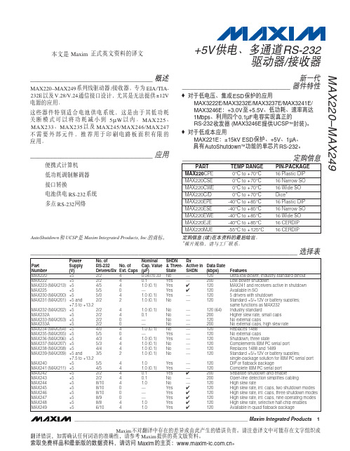
General DescriptionThe MAX200–MAX211/MAX213 transceivers are designed for RS-232 and V.28 communication inter-faces where ±12V supplies are not available. On-board charge pumps convert the +5V input to the ±10V need-ed for RS-232 output levels. The MAX201 and MAX209operate from +5V and +12V, and contain a +12V to -12V charge-pump voltage converter.The MAX200–MAX211/MAX213 drivers and receivers meet all EIA/TIA-232E and CCITT V.28 specifications at a data rate of 20kbps. The drivers maintain the ±5V EIA/TIA-232E output signal levels at data rates in excess of 120kbps when loaded in accordance with the EIA/TIA-232E specification.The 5µW shutdown mode of the MAX200, MAX205,MAX206, and MAX211 conserves energy in battery-powered systems. The MAX213 has an active-low shut-down and an active-high receiver enable control. Two receivers of the MAX213 are active, allowing ring indica-tor (RI) to be monitored easily using only 75µW power.The MAX211 and MAX213 are available in a 28-pin wide small-outline (SO) package and a 28-pin shrink small-outline (SSOP) package, which occupies only 40% of the area of the SO. The MAX207 is now avail-able in a 24-pin SO package and a 24-pin SSOP. The MAX203 and MAX205 use no external components,and are recommended for applications with limited circuit board space.ApplicationsComputersLaptops, Palmtops, Notebooks Battery-Powered Equipment Hand-Held Equipment Next-Generation Device Features ♦For Low-Cost Applications:MAX221E: ±15kV ESD-Protected, +5V, 1µA, Single RS-232 Transceiver with AutoShutdown™♦For Low-Voltage and Space-Constrained Applications:MAX3222E/MAX3232E/MAX3237E/MAX3241E/MAX3246E: ±15kV ESD-Protected, Down to 10nA,+3.0V to +5.5V, Up to 1Mbps, True RS-232Transceivers (MAX3246E Available in UCSP™Package)♦For Space-Constrained Applications:MAX3228E/MAX3229E: ±15kV ESD-Protected,+2.5V to +5.5V, RS-232 Transceivers in UCSP ♦For Low-Voltage or Data Cable Applications:MAX3380E/MAX3381E: +2.35V TO +5.5V, 1µA,2Tx/2Rx RS-232 Transceivers with ±15kV ESD-Protected I/O and Logic Pins ♦For Low-Power Applications:MAX3224E–MAX3227E/MAX3244E/MAX3245E:±15kV ESD-Protected, 1µA, 1Mbps, +3.0V to+5.5V, RS-232 Transceivers with AutoShutdown Plus™MAX200–MAX211/MAX213+5V , RS-232 Transceivers with 0.1µF External Capacitors ________________________________________________________________Maxim Integrated Products 119-0065; Rev 6; 10/03For pricing, delivery, and ordering information,please contact Maxim/Dallas Direct!at 1-888-629-4642, or visit Maxim’s website at .Ordering Information appears at end of data sheetAutoShutdown, AutoShutdown Plus, and UCSP are trademarks of Maxim Integrated Products, Inc.MAX200–MAX211/MAX213+5V , RS-232 Transceiverswith 0.1µF External Capacitors______________________________________________________________________________________19Ordering Information*Contact factory for dice specifications.M A X 200–M A X 211/M A X 213+5V , RS-232 Transceiverswith 0.1µF External Capacitors Maxim cannot assume responsibility for use of any circuitry other than circuitry entirely embodied in a Maxim product. No circuit patent licenses are implied. Maxim reserves the right to change the circuitry and specifications without notice at any time.20____________________Maxim Integrated Products, 120 San Gabriel Drive, Sunnyvale, CA 94086 408-737-7600©2003 Maxim Integrated ProductsPrinted USAis a registered trademark of Maxim Integrated Products.Package Information(The package drawing(s) in this data sheet may not reflect the most current specifications. For the latest package outline information,go to /packages .)。


________________General DescriptionThe MAX1668/MAX1805/MAX1989 are precise multi-channel digital thermometers that report the tempera-ture of all remote sensors and their own packages. The remote sensors are diode-connected transistors—typi-cally low-cost, easily mounted 2N3904 NPN types—that replace conventional thermistors or thermocouples.Remote accuracy is ±3°C for multiple transistor manu-facturers, with no calibration needed. The remote chan-nels can also measure the die temperature of other ICs,such as microprocessors, that contain an on-chip,diode-connected transistor.The 2-wire serial interface accepts standard system management bus (SMBus™) write byte, read byte, send byte, and receive byte commands to program the alarm thresholds and to read temperature data. The data for-mat is 7 bits plus sign, with each bit corresponding to 1°C, in two’s-complement format.The MAX1668/MAX1805/MAX1989 are available in small, 16-pin QSOP surface-mount packages. The MAX1989 is also available in a 16-pin TSSOP.________________________Applications____________________________Featureso Multichannel4 Remote, 1 Local (MAX1668/MAX1989)2 Remote, 1 Local (MAX1805)o No Calibration Required o SMBus 2-Wire Serial Interfaceo Programmable Under/Overtemperature Alarms o Supports SMBus Alert Response o Accuracy±2°C (+60°C to +100°C, Local)±3°C (-40°C to +125°C, Local)±3°C (+60°C to +100°C, Remote)o 3µA (typ) Standby Supply Current o 700µA (max) Supply Currento Small, 16-Pin QSOP/TSSOP PackagesMAX1668/MAX1805/MAX1989†Multichannel Remote/LocalTemperature Sensors________________________________________________________________Maxim Integrated Products119-1766; Rev 2; 5/03SMBus is a trademark of Intel Corp.†Patents PendingDesktop and Notebook Computers LAN Servers Industrial ControlsCentral-Office Telecom EquipmentTest and Measurement Multichip ModulesFor pricing, delivery, and ordering information,please contact Maxim/Dallas Direct!at 1-888-629-4642, or visit Maxim’s website at .M A X 1668/M A X 1805/M A X 1989†Multichannel Remote/Local Temperature Sensors 2_______________________________________________________________________________________ABSOLUTE MAXIMUM RATINGSELECTRICAL CHARACTERISTICS(V CC = +3.3V, STBY = V CC , configuration byte = X0XXXX00, T A = 0°C to +125°C , unless otherwise noted.)Stresses beyond those listed under “Absolute Maximum Ratings” may cause permanent damage to the device. These are stress ratings only, and functional operation of the device at these or any other conditions beyond those indicated in the operational sections of the specifications is not implied. Exposure to absolute maximum rating conditions for extended periods may affect device reliability.V CC to GND..............................................................-0.3V to +6V DXP_, ADD_, STBY to GND........................-0.3V to (V CC + 0.3V)DXN_ to GND ........................................................-0.3V to +0.8V SMBCLK, SMBDATA, ALERT to GND......................-0.3V to +6V SMBDATA, ALERT Current.................................-1mA to +50mA DXN_ Current......................................................................±1mA Continuous Power Dissipation (T A = +70°C)QSOP (derate 8.30mW/°C above +70°C)....................667mW TSSOP (derate 9.40mW/°C above +70°C)..................755mWOperating Temperature Range .........................-55°C to +125°C Junction Temperature......................................................+150°C Storage Temperature Range.............................-65°C to +150°C Lead Temperature (soldering, 10s).................................+300°CMAX1668/MAX1805/MAX1989†Multichannel Remote/LocalTemperature Sensors_______________________________________________________________________________________3ELECTRICAL CHARACTERISTICS (continued)(V CC = +3.3V, STBY = V CC , configuration byte = X0XXXX00, T A = 0°C to +125°C , unless otherwise noted.)ELECTRICAL CHARACTERISTICS(V CC = +5V, STBY = V CC , configuration byte = X0XXXX00, T A = -55°C to +125°C , unless otherwise noted.) (Note 6)08416122024FREQUENCY (MHz)T E M P E R A T U R E E R R O R (°C )TEMPERATURE ERROR vs. SUPPLY NOISE FREQUENCY0.111010020-20110100TEMPERATURE ERROR vs. PC BOARD RESISTANCE-10LEAKAGE RESISTANCE (M Ω)T E M P E R A T U R E E R R O R (°C )10-2-101234-50-10-301030507090110TEMPERATURE ERROR vs. TEMPERATURETEMPERATURE (°C)T E M P E R A T U R E E R R O R (°C )Typical Operating Characteristics(Typical Operating Circuit , V CC = +5V, STBY = V CC , configuration byte = X0XXXX00, T A = +25°C, unless otherwise noted.)M A X 1668/M A X 1805/M A X 1989†Multichannel Remote/Local Temperature Sensors 4_______________________________________________________________________________________ELECTRICAL CHARACTERISTICS (continued)(V= +5V, STBY = V , configuration byte = X0XXXX00, T = -55°C to +125°C , unless otherwise noted.) (Note 6)Note 1:Guaranteed by design, but not production tested.Note 2:Quantization error is not included in specifications for temperature accuracy. For example, if the MAX1668/MAX1805/MAX1989 device temperature is exactly +66.7°C, the ADC may report +66°C, +67°C, or +68°C (due to the quantization error plus the +0.5°C offset used for rounding up) and still be within the guaranteed ±1°C error limits for the +60°C to +100°C temperature range. See Table 2.Note 3: A remote diode is any diode-connected transistor from Table 1. T R is the junction temperature of the remote diode. See theRemote-Diode Selection section for remote-diode forward-voltage requirements.Note 4:The SMBus logic block is a static design that works with clock frequencies down to DC. While slow operation is possible, itviolates the 10kHz minimum clock frequency and SMBus specifications, and can monopolize the bus.Note 5:Note that a transition must internally provide at least a hold time in order to bridge the undefined region (300ns max) ofSMBCLK’s falling edge t HD:DAT.Note 6:Specifications from -55°C to +125°C are guaranteed by design, not production tested.020406080100120140160012345STANDBY SUPPLY CURRENT vs. SUPPLY VOLTAGESUPPLY VOLTAGE (V)S U P P L Y C U R R E N T (µA )257550100125-220468RESPONSE TO THERMAL SHOCKTIME (s)T E M P E R A T U R E (°C )MAX1668/MAX1805/MAX1989†Multichannel Remote/LocalTemperature Sensors_______________________________________________________________________________________50.111000TEMPERATURE ERRORvs. COMMON-MODE NOISE FREQUENCYFREQUENCY (MHz)T E M P E R A T U R E E R R O R (°C )1010000.60.40.20.81.01.21.41.61.82.0Typical Operating Characteristics (continued)(Typical Operating Circuit , V CC = +5V, STBY = V CC , configuration byte = X0XXXX00, T A = +25°C, unless otherwise noted.)TEMPERATURE ERRORvs. DXP_ TO DXN_ CAPACITANCEM A X 16681805 t o c 05DXP_ TO DXN_ CAPACITANCE (nF)T E M P E R A T U R E E R R O R (°C )-10-6-8-2-42040203010405060STANDBY SUPPLY CURRENT vs. CLOCK FREQUENCYSMBCLK FREQUENCY (kHz)S U P P L Y C U R R E N T (µA )6010203040501101001000M A X 1668/M A X 1805/M A X 1989†Multichannel Remote/Local Temperature Sensors 6______________________________________________________________________________________________________Detailed DescriptionThe MAX1668/MAX1805/MAX1989 are temperature sensors designed to work in conjunction with an exter-nal microcontroller (µC) or other intelligence in thermo-static, process-control, or monitoring applications. The µC is typically a power-management or keyboard con-troller, generating SMBus serial commands by “bit-banging” general-purpose input-output (GPIO) pins or through a dedicated SMBus interface block.These devices are essentially 8-bit serial analog-to-digi-tal converters (ADCs) with sophisticated front ends.However, the MAX1668/MAX1805/MAX1989 also contain a switched current source, a multiplexer, an ADC, an SMBus interface, and associated control logic (Figure 1).In the MAX1668 and MAX1989, temperature data from the ADC is loaded into five data registers, where it is automatically compared with data previously stored in 10 over/undertemperature alarm registers. In the MAX1805, temperature data from the ADC is loaded into three data registers, where it is automatically compared with data previously stored in six over/undertemperature alarm registers.ADC and MultiplexerThe ADC is an averaging type that integrates over a 64ms period (each channel, typical), with excellent noise rejection.The multiplexer automatically steers bias currents through the remote and local diodes, measures their forward voltages, and computes their temperatures.Each channel is automatically converted once the con-version process has started. If any one of the channels is not used, the device still performs measurements on these channels, and the user can ignore the results of the unused channel. If any remote-diode channel is unused, connect DXP_ to DXN_ rather than leaving the pins open.The DXN_ input is biased at 0.65V above ground by an internal diode to set up the A/D inputs for a differential measurement. The worst-case DXP_ to DXN_ differential input voltage range is 0.25V to 0.95V.Excess resistance in series with the remote diode caus-es about +0.5°C error per ohm. Likewise, 200µV of offset voltage forced on DXP_ to DXN_causes about 1°C error.MAX1668/MAX1805/MAX1989†Multichannel Remote/LocalTemperature Sensors_______________________________________________________________________________________7Figure 1. MAX1668/MAX1805/MAX1989 Functional DiagramA/D Conversion SequenceIf a start command is written (or generated automatically in the free-running autoconvert mode), all channels are converted, and the results of all measurements are available after the end of conversion. A BUSY status bit in the status byte shows that the device is actually per-forming a new conversion; however, even if the ADC is busy, the results of the previous conversion are always available.Remote-Diode SelectionTemperature accuracy depends on having a good-qual-ity, diode-connected small-signal transistor. Accuracy has been experimentally verified for all of the devices listed in Table 1. The MAX1668/MAX1805/MAX1989 can also directly measure the die temperature of CPUs and other ICs having on-board temperature-sensing diodes.The transistor must be a small-signal type, either NPN or PNP, with a relatively high forward voltage; other-wise, the A/D input voltage range can be violated. The forward voltage must be greater than 0.25V at 10µA;check to ensure this is true at the highest expected temperature. The forward voltage must be less than 0.95V at 100µA; check to ensure this is true at the low-est expected temperature. Large power transistors do not work at all. Also, ensure that the base resistance is less than 100Ω. Tight specifications for forward-current gain (+50 to +150, for example) indicate that the manu-facturer has good process controls and that the devices have consistent VBE characteristics.F or heat-sink mounting, the 500-32BT02-000 thermal sensor from Fenwal Electronics is a good choice. This device consists of a diode-connected transistor, an aluminum plate with screw hole, and twisted-pair cable (Fenwal Inc., Milford, MA, 508-478-6000).Thermal Mass and Self-HeatingThermal mass can seriously degrade the MAX1668/MAX1805/MAX1989s’ effective accuracy. The thermal time constant of the 16-pin QSOP package is about 140s in still air. F or the MAX1668/MAX1805/MAX1989junction temperature to settle to within +1°C after a sudden +100°C change requires about five time con-stants or 12 minutes. The use of smaller packages for remote sensors, such as SOT23s, improves the situa-tion. Take care to account for thermal gradients between the heat source and the sensor, and ensure that stray air currents across the sensor package do not interfere with measurement accuracy.Self-heating does not significantly affect measurement accuracy. Remote-sensor self-heating due to the diode current source is negligible. F or the local diode, theworst-case error occurs when sinking maximum current at the ALERT output. For example, with ALERT sinking 1mA, the typical power dissipation is V CC x 400µA plus 0.4V x 1mA. Package theta J-A is about 150°C/W, so with V CC = 5V and no copper PC board heat sinking,the resulting temperature rise is:dT = 2.4mW x 150°C/W = 0.36°CEven with these contrived circumstances, it is difficult to introduce significant self-heating errors.ADC Noise FilteringThe ADC is an integrating type with inherently good noise rejection, especially of low-frequency signals such as 60Hz/120Hz power-supply hum. Micropower opera-tion places constraints on high-frequency noise rejec-tion; therefore, careful PC board layout and proper external noise filtering are required for high-accuracy remote measurements in electrically noisy environments. High-frequency EMI is best filtered at DXP_ and DXN_with an external 2200pF capacitor. This value can be increased to about 3300pF (max), including cable capacitance. Higher capacitance than 3300pF intro-duces errors due to the rise time of the switched cur-rent source.Nearly all noise sources tested cause additional error measurements, typically by +1°C to +10°C, depending on the frequency and amplitude (see the Typical Operating Characteristics ).PC Board Layout1)Place the MAX1668/MAX1805/MAX1989 as close aspractical to the remote diode. In a noisy environment,such as a computer motherboard, this distance canM A X 1668/M A X 1805/M A X 1989†Multichannel Remote/Local Temperature Sensors 8_______________________________________________________________________________________Table 1. Remote-Sensor Transistor ManufacturersNote:Transistors must be diode connected (base shorted to collector).be 4in to 8in (typ) or more as long as the worst noise sources (such as CRTs, clock generators, memory buses, and ISA/PCI buses) are avoided.2)Do not route the DXP_ to DXN_ lines next to thedeflection coils of a CRT. Also, do not route the traces across a fast memory bus, which can easily introduce +30°C error, even with good filtering.Otherwise, most noise sources are fairly benign.3)Route the DXP_ and DXN_ traces in parallel and inclose proximity to each other, away from any high-voltage traces such as +12VDC. Leakage currents from PC board contamination must be dealt with carefully, since a 20M Ωleakage path from DXP_ to ground causes about +1°C error.4)Connect guard traces to GND on either side of theDXP_ to DXN_ traces (Figure 2). With guard traces in place, routing near high-voltage traces is no longer an issue. 5)Route through as few vias and crossunders as possi-ble to minimize copper/solder thermocouple effects. 6)When introducing a thermocouple, make sure thatboth the DXP_ and the DXN_ paths have matching thermocouples. In general, PC board-induced ther-mocouples are not a serious problem. A copper-sol-der thermocouple exhibits 3µV/°C, and it takes about 200µV of voltage error at DXP_ to DXN_ to cause a +1°C measurement error. So, most para-sitic thermocouple errors are swamped out.7)Use wide traces. Narrow ones are more inductiveand tend to pick up radiated noise. The 10mil widths and spacings recommended in Figure 2 are not absolutely necessary (as they offer only a minor improvement in leakage and noise), but try to use them where practical.8)Copper cannot be used as an EMI shield, and onlyferrous materials such as steel work well. Placing a copper ground plane between the DXP_ to DXN_traces and traces carrying high-frequency noise sig-nals does not help reduce EMI.PC Board Layout Checklist•Place the MAX1668/MAX1805/MAX1989as close as possible to the remote diodes.•Keep traces away from high voltages (+12V bus).•Keep traces away from fast data buses and CRTs.•Use recommended trace widths and spacings.•Place a ground plane under the traces.•Use guard traces flanking DXP_ and DXN_ and con-necting to GND.•Place the noise filter and the 0.1µF V CC bypass capacitors close to the MAX1668/MAX1805/MAX1989.•Add a 200Ωresistor in series with V CC for best noise filtering (see the Typical Operating Circuit ).Twisted-Pair and Shielded CablesFor remote-sensor distances longer than 8in, or in partic-ularly noisy environments, a twisted pair is recommend-ed. Its practical length is 6ft to 12ft (typ) before noise becomes a problem, as tested in a noisy electronics lab-oratory. F or longer distances, the best solution is a shielded twisted pair like that used for audio micro-phones. For example, Belden #8451 works well for dis-tances up to 100ft in a noisy environment. Connect the twisted pair to DXP_ and DXN_ and the shield to GND,and leave the shield’s remote end unterminated.Excess capacitance at DX_ _ limits practical remote-sen-sor distances (see the Typical Operating Characteristics ).F or very long cable runs, the cable’s parasitic capaci-tance often provides noise filtering, so the 2200pF capac-itor can often be removed or reduced in value.Cable resistance also affects remote-sensor accuracy;1Ωseries resistance introduces about +0.5°C error.Low-Power Standby ModeStandby mode disables the ADC and reduces the sup-ply-current drain to less than 12µA. Enter standby mode by forcing the STBY pin low or through the RUN/STOP bit in the configuration byte register.Hardware and software standby modes behave almost identically: all data is retained in memory, and the SMB interface is alive and listening for reads and writes.Activate hardware standby mode by forcing the STBY pin low. In a notebook computer, this line can be con-nected to the system SUSTAT# suspend-state signal. The STBY pin low state overrides any software conversion command. If a hardware or software standby command is received while a conversion is in progress, the conver-MAX1668/MAX1805/MAX1989†Multichannel Remote/LocalTemperature Sensors_______________________________________________________________________________________9Figure 2. Recommended DXP_/DXN_ PC Tracession cycle is truncated, and the data from that conversion is not latched into either temperature-reading register. The previous data is not changed and remains available.In standby mode, supply current drops to about 3µA.At very low supply voltages (under the power-on-reset threshold), the supply current is higher due to the address pin bias currents. It can be as high as 100µA,depending on ADD0 and ADD1 settings.SMBus Digital InterfaceF rom a software perspective, the MAX1668/MAX1805/MAX1989appear as a set of byte-wide registers that contain temperature data, alarm threshold values, or control bits. A standard SMBus 2-wire serial interface is used to read temperature data and write control bits and alarm threshold data. Each A/D channel within the devices responds to the same SMBus slave address for normal reads and writes.The MAX1668/MAX1805/MAX1989employ four standard SMBus protocols: write byte, read byte, send byte, and receive byte (Figure 3). The shorter receive byte protocol allows quicker transfers, provided that the correct data register was previously selected by a read byte instruc-tion. Use caution with the shorter protocols in multimaster systems, since a second master could overwrite the com-mand byte without informing the first master.The temperature data format is 7 bits plus sign in two’s-com-plement form for each channel, with each data bit represent-ing 1°C (Table 2), transmitted MSB first. Measurements are offset by +0.5°C to minimize internal rounding errors; for example, +99.6°C is reported as +100°C.Alarm Threshold RegistersTen (six for MAX1805) registers store alarm threshold data, with high-temperature (T HIGH ) and low-tempera-ture (T LOW ) registers for each A/D channel. If either measured temperature equals or exceeds the corre-sponding alarm threshold value, an ALERT interrupt is asserted.The power-on-reset (POR) state of all T HIGH registers of the MAX1668 and MAX1805 is full scale (0111 1111, or +127°C). The POR state of the channel 1 T HIGH register of the MAX1989 is 0110 1110 or +110°C, while all other channels are at +127°C. The POR state of all T LOW reg-isters is 1100 1001 or -55°C.M A X 1668/M A X 1805/M A X 1989†Multichannel Remote/Local Temperature Sensors 10______________________________________________________________________________________Figure 3. SMBus ProtocolsThere is a continuity fault detector at DXP_ that detects whether the remote diode has an open-circuit condi-tion. At the beginning of each conversion, the diode fault is checked, and the status byte is updated. This fault detector is a simple voltage detector; if DXP_ rises above V CC - 1V (typ) due to the diode current source, a fault is detected. Note that the diode fault is not checked until a conversion is initiated, so immediately after power-on reset, the status byte indicates no fault is present, even if the diode path is broken.If any remote channel is shorted (DXP_ to DXN_ or DXP_ to GND), the ADC reads 0000 0000 so as not to trip either the T HIGH or T LOW alarms at their POR set-tings. In applications that are never subjected to 0°C in normal operation, a 0000 0000 result can be checked to indicate a fault condition in which DXP_ is acciden-tally short circuited. Similarly, if DXP_ is short circuited to V CC , the ADC reads +127°C for all remote and local channels, and the device alarms.A L E R T InterruptsThe ALERT interrupt output signal is latched and can only be cleared by reading the alert response address.Interrupts are generated in response to T HIGH and T LOW comparisons and when a remote diode is disconnected (for continuity fault detection). The interrupt does not halt automatic conversions; new temperature data continues to be available over the SMBus interface after ALERT is asserted. The interrupt output pin is open drain so that devices can share a common interrupt line. The interrupt rate can never exceed the conversion rate.The interface responds to the SMBus alert response address, an interrupt pointer return-address feature (see Alert R esponse Address section). Prior to taking corrective action, always check to ensure that an inter-rupt is valid by reading the current temperature.Alert Response AddressThe SMBus alert response interrupt pointer provides quick fault identification for simple slave devices that lack the complex, expensive logic needed to be a bus master. Upon receiving an ALERT interrupt signal, the host master can broadcast a receive byte transmission to the alert response slave address (0001 100). Then any slave device that generated an interrupt attempts to identify itself by putting its own address on the bus (Table 3).The alert response can activate several different slave devices simultaneously, similar to the I 2C general call. If more than one slave attempts to respond, bus arbitra-tion rules apply, and the device with the lower address code wins. The losing device does not generate an acknowledge and continues to hold the ALERT line low until serviced (implies that the host interrupt input isMAX1668/MAX1805/MAX1989†Multichannel Remote/LocalTemperature Sensors______________________________________________________________________________________11Table 3. Read Format for Alert Response Address (0001100)ADD66Provide the currentMAX1668/MAX1805/MAX1989slave address that was latched at POR (Table 8)FUNCTIONADD55ADD44ADD33ADD22ADD11ADD77(MSB)10(LSB)Logic 1BIT NAMElevel sensitive). Successful reading of the alert response address clears the interrupt latch.Command Byte FunctionsThe 8-bit command byte register (Table 4) is the master index that points to the various other registers within the MAX1668/MAX1805/MAX1989. The register ’s PORstate is 0000 0000, so that a receive byte transmission (a protocol that lacks the command byte) that occurs immediately after POR returns the current local temper-ature data.M A X 1668/M A X 1805/M A X 1989†Multichannel Remote/Local Temperature Sensors 12______________________________________________________________________________________**Not available for MAX1805.MAX1668/MAX1805/MAX1989†Multichannel Remote/LocalTemperature Sensors______________________________________________________________________________________13Manufacturer and DeviceID CodesTwo ROM registers provide manufacturer and device ID codes. Reading the manufacturer ID returns 4Dh,which is the ASCII code M (for Maxim). Reading the device ID returns 03h for MAX1668, 05h for MAX1805,and 0Bh for MAX1989. If the read word 16-bit SMBus protocol is employed (rather than the 8-bit Read Byte),the least significant byte contains the data and the most significant byte contains 00h in both cases.Configuration Byte FunctionsThe configuration byte register (Table 5) is used to mask (disable) interrupts and to put the device in soft-ware standby mode.Status Byte FunctionsThe two status byte registers (Tables 6 and 7) indicate which (if any) temperature thresholds have been exceeded. The first byte also indicates whether the ADC is converting and whether there is an open circuit in a remote-diode DXP_ to DXN_ path. After POR, the normal state of all the flag bits is zero, assuming none of the alarm conditions are present. The status byte is cleared by any successful read of the status byte,unless the fault persists. Note that the ALERT interrupt latch is not automatically cleared when the status flag bit is cleared.When reading the status byte, you must check for inter-nal bus collisions caused by asynchronous ADC timing,or else disable the ADC prior to reading the status byte (through the RUN/STOP bit in the configuration byte).To check for internal bus collisions, read the status byte. If the least significant 7 bits are ones, discard the data and read the status byte again. The status bits LHIGH, LLOW, RHIGH, and RLOW are refreshed on the SMBus clock edge immediately following the stop con-dition, so there is no danger of losing temperature-relat-ed status data as a result of an internal bus collision.The OPEN status bit (diode continuity fault) is only refreshed at the beginning of a conversion, so OPEN data is lost. The ALERT interrupt latch is independent of the status byte register, so no false alerts are generated by an internal bus collision.If the THIGH and TLOW limits are close together, it ’s possible for both high-temp and low-temp status bits to be set, depending on the amount of time between sta-tus read operations (especially when converting at the fastest rate). In these circumstances, it ’s best not to relyon the status bits to indicate reversals in long-term tem-perature changes and instead use a current tempera-ture reading to establish the trend direction.Conversion RateThe MAX1668/MAX1805/MAX1989 are continuously measuring temperature on each channel. The typical conversion rate is approximately three conversions/s (for both devices). The resulting data is stored in the temperature data registers.Slave AddressesThe MAX1668/MAX1805/MAX1989 appear to the SMBus as one device having a common address for all ADC channels. The device address can be set to one of nine different values by pin-strapping ADD0 and ADD1 so that more than one MAX1668/MAX1805/MAX1989 can reside on the same bus without address conflicts (Table 8).The address pin states are checked at POR only, and the address data stays latched to reduce quiescent supply current due to the bias current needed for high-Z state detection.The MAX1668/MAX1805/MAX1989 also respond to the SMBus alert response slave address (see the Alert Response Address section).POR and Undervoltage LockoutThe MAX1668/MAX1805/MAX1989 have a volatile memory. To prevent ambiguous power-supply condi-tions from corrupting the data in memory and causing erratic behavior, a POR voltage detector monitors V CC and clears the memory if V CC falls below 1.8V (typ, see the Electrical Characteristics table). When power is first applied and V CC rises above 1.85V (typ), the logic blocks begin operating, although reads and writes at V CC levels below 3V are not recommended. A second V CC comparator, the ADC UVLO comparator, prevents the ADC from converting until there is sufficient head-room (V CC = 2.8V typ).Power-Up Defaults•Interrupt latch is cleared.•Address select pins are sampled.•ADC begins converting.•Command byte is set to 00h to facilitate quick remote receive byte queries.•T HIGH and T LOW registers are set to max and min limits, respectively.。