PESD12VS1UB中文资料
- 格式:pdf
- 大小:111.43 KB
- 文档页数:15


ESD介绍ESD( Electro Static Discharge)中文——---静电放电。
日常生活中的ESD如闪电放电,行走中的人对金属把手放电。
日常生活中的ESD开关显示器时用手触摸屏幕夜晚穿脱毛衣时能看到会有轻微的滋滋放电声电火花的出现。
静电如何产生?一.摩擦正常情况下材料A与B呈电中性,摩擦后材料A带正电B带负电材料A材料B 材料A材料B静电放电的模型 1 人體放電模式(Human-Body Model,HBM)静电放电的模型 2 機器放電模式(Machine Model,MM)静电放电的模型.3 元件充電模式(Charged-DeviceModel, CDM)5000VHear4500VTouch3500VComponent为何要做ESD防护由于电子行业的迅速发展,体积小、集成度高的器件得到大规模生产,从而导致导线间距越来越小,绝缘膜越来越薄,致使耐击穿电压也愈来愈低。
而电子产品在生产、运输、储存和转运等过程中所产生的静电电压却远远超过其击穿电压阈值,这就可能造成器件的击穿或失效,影响产品的技术指标,降低其可靠性。
静电对电子产品的主要影响软击穿则可使器件的性能劣化,并使其指标参数降低而造成故障隐患。
且不易被发现,软击穿时设备仍能带"病"工作,性能未发生根本变化,很可能通过出厂检验,但随时可能造成再次失效。
多次软击穿就能造成硬击穿,既给用户造成损失,也影响厂家声誉和产品的销售“软击穿如负伤而行的人”而不幸的是ESD损害大多为软击穿ESD防护推行的难点静电控制的困难1.静电如细菌,无处不在。
2.认证静电的破坏工作困难成本高。
3.需要全体人员的配合,特别是高层管理者的支持。
4.实施的成本压力可能不低(尤其在相对低的劳动力市场)5.防静电技术的复杂性容易被忽视,随机性也特强。
6.缺乏精确性(难以要求)测量技术也受到限制。
一ESD防护推行的难点静电对电子产品损害有哪些特点一.隐蔽性:人体感觉到的静电已达3000v二.潜在性: 大部分静电破坏是潜在的不能马上识别。

E S D 静电放电1、参考文件标准GB/T19951-20052、ESD模拟器a)电压范围:-25Kv~+25Kvb)电容:330pF土10%,150pF土10%(两个放电端)c)电阻:2000 Q ± 10%d)上升沿时间:1)直接接触,0.7ns~1 ns (2 Q负载时);(通用为w 1ns)2)空气放电,w 5ns (2 Q负载时);(通用为w 20ns)测试期间,使周围环境温度保持在(23± 3)C,相对湿度为30%-60% (首选20C和30%的相对湿度)。
3、ESD设备工作时的测试(通电状态)接触放电法(接触放电端)和330Pf的电容空气放电法(空气放电端)和330Pf的电容DUT可以按照表1的规定发生功能偏移。
需要在测试之前和测试完成后对DUT I/O的参数值(例如:阻抗,电容,泄漏电流等)进行确认。
如果测试完成以后,参数值超过其规定范围,则该DUT为非兼容性。
各放电试验点在每种电压等级下承受至少3次正电压放电和3次负电压放电,放电间隔最少5s.在每种电压等级下,设备的放电试验点先承受一种极性的放电试验,再承受反极性的放电试验。
在每连续3次放电试验期间和之后,检验被试设备是否符合所有使用功能的要求。
CI电源线瞬态现象参考文件标准ISO-7637-2、ISO-7637-3一、电瞬态传导试验ISO-7637-21、试验条件车载信息娱乐系统主机在沿电源线的电瞬态传导试验中应能正常工作,符合ISO-7637-2标准,川级。
1)试验温度和试验电压试验周围环境温度应为23 C±5C。
试验电压为表1所示试验脉冲发生器应能在I U S I为最大值时产生 2.1 )至2.5 )条描述的开路试验脉冲。
此外,U S应能在表2至表8所给的限值内可调。
2、试验过程2.1试验脉冲1本试验室模拟电源与感性负载断开连接时所产生的瞬态现象。
它适用于各种DUT在车辆上使用时,与感性负载保持直接并联的情况。


Manual and Installation GuideBB10012, BB5012, BBGC2Table of contents•Charging parameters•BMS functions•Installation•Storage and maintenance •Warranty•Returns•Contact usCongratulations you have purchased one of the top 12vbatteries on the marketAt Battle Born Batteries we do everything we can to make our batteries compatible with all the existing products on the market, unfortunately there are a few that slip through the cracks. This manual will serve as a guideline to check and see if your current charger will work with your new Battle Born Battery. Published on our website () is also a list of chargers we have found to be compatible with our batteries.Bulk/AbsorptionFor your Bulk/Absorption stage, the ideal voltage is between 14.2v-14.6v. This range will allow the battery to fully charge any higher then this and the built in BMS will send the battery into a protect mode.FloatOur batteries do not need to float so setting your Float voltage to 13.6v or lower will be in the range of its natural float level.EqualizationEqualization is not recommended for our batteries. Most chargers will allow you to shut this feature off or use a setting that does not use equalization. If you cannot turn off this mode then you will need to adjust the voltage to below 14.6vTemperature CompensationTemperature compensation is not needed with our batteries and in some cases, may trigger the built in BMS to go into protect mode. For this reason, we recommend that temperature compensation be shut off or set to 0.BMS Basic FeaturesAll Battle Born Batteries come with a built-in battery management system (BMS). Our BMS allows us to create one of the safest LiFeP04 batteries on the planet. To help us keep our promise that our batteries will last for 3-5000 cycles, our BMS will put the battery into a protect mode in the event the battery falls outside of one of the following parameters.High voltage: 14.7v-15.0vWill not allow any more current into the battery.Low voltage: 9.0v-10.5vWill not allow a discharge from the battery. (Note: many chargers must detect a voltage over 10v to send a charge to the battery).High temperature: 135FWill not allow a charge or discharge.Low temperature: 25FWill not allow a chargeHigh CurrentThe current exceeds 100 (+/- 5%) Amps for 30s or 200 (+/- 10%) Amps for 0.5s (this is interpreted as a short circuit)Allowable outputThe BMS constantly monitors the batteries output. We have set the following parameters to ensure our batteries maintain a high level of safety.BB10012 BB5012Surge: 200a for 30 seconds Surge: 100a for 30 secondsContinuous: 100a Continuous: 60aNote: Higher current capabilities for ½ second. In all Cases the battery recovers automaticallyCell BalancingAt Battle Born Batteries we pride ourselves on making the highest quality product that we can. We have found the best way for us to do this is to capacity match the entire way, from the 120 cells to the 4 modules to however many batteries are in your bank just know that they have been specifically selected to give you the best performance. A concern that some customers have is cell balancing. We built passive cell balancing into OUR BMS so that you never have to worry about your battery becoming unbalanced.InstallationOur batteries are rather straight forward to install, simply connect your positive cables to the positive terminals and your negative cables to the negative terminal. Our batteries work great in either parallel or series configurations (up to 48v). Our batteries come standard with a flag style terminal post. These terminals include a 3/8” hole that allows for most ring terminals to work well with our batteries. For the best connection, we recommend either copper or brass ring terminals.ParallelMultiple BB10012 may be mounted in parallel in order to increase the current capacity of the system. When batteries are mounted in parallel, the voltage of the system does not change, but the current limits are additive. For example, two BB10012 batteries mounted in parallel can deliver 200A continuously and 400A for 30 seconds. Three BB10012 batteries mounted in parallel can deliver 300A continuously and 600A for 30 seconds. Therefore, all cables and connections MUST be able to accommodate the high currents that can be delivered by the battery. Appropriate fuses and circuit breakers are also highly recommended to protect downstream components from current spikes and short circuits.SeriesTwo BB10012 may be mounted in series to increase the voltage of the system up to a 48V system.** (see note below) When batteries are mounted in series, current capacities remain the same, but the system voltage is additive. Two BB10012 batteries mounted in series to form a nominally 24V systemshould be charged using a bulk and absorption voltage of 28.8V, and a float voltage below 27.2V. Four Batteries connected in series form a 48 volt system.*Our batteries work with trolling motors in 12, 24, 36, 48 volts and do not need anything extra equipment, we do recommend that you use a multibank charger. We work well with most brands Dual Pro, Minkota, Noco et. If you have a question about charging give us call 855-292-2831 or email ******************************.*We can support systems up to 48 volts with our Battle Born Batteries. For 24 and 48 volt systems using inverters and inverter chargers will need an extra piece of equipment to “soft start” the capacitors of these devices. If you are using a 24 or 48 volt inverter charger or any DC device with large capacitors such as a heat pump, give us a call 855-292-2831, so we can help you set up your system.Storage and maintenanceStorageStorage could not be easier simply charge the batteries fully and disconnect from any charge or discharge.MaintenanceBattle Born Batteries require very little maintenance if any at all. If your batteries are in series and not being charged by a multi-bank charger it is recommended that you fully charge the batteries individually once a year. This will balance out the entire battery bank to ensure the batteries will reach its expected life span. If your batteries are in parallel this is not necessary. Our BMS has a built in passive balancing system that will take care of this for you.Warranty PolicyIn the unlikely event, you are having an issue with one of our batteries we have developed a straight forward warranty policy to help answer any questions you may have.Battle Born Batteries offers a 3 year manufacturers defect warranty from the date of purchase. This warranty does not cover negligence or misuse of the battery. If it is deemed that battery was used improperly, you will be subject to a $150 an hour repair charge plus parts and shipping.We also warrant all other complimentary products (inverters, converters, chargers etc) we sell are free from defect for 30 days from the date of purchase. After that time it is the responsibility of our manufacturing partners and a standard manufacturer’s warranty applies (1 year from date of purchase, unless otherwise stated by the manufacturer).Return & Refund PolicyThanks for shopping at Battle Born Batteries. If you are not entirely satisfied with your purchase, we're here to help.ReturnsYou have 45 calendar days to return an item from the date the item shipped. To be eligible for a return, your item must be in the same condition that you received it in. Your item must be in the original packaging. Your item needs to have the receipt or proof of purchase.RefundsOnce we receive your item, we will inspect it and notify you that we have received your returned item. We will immediately notify you on the status of your refund after inspecting the item. If your return is approved, we will initiate a refund to your credit card (or original method of payment). You will receive the credit within a certain amount of days, depending on your card issuer's policies. ShippingYou will be responsible for paying for your own shipping costs for returning your item. Shipping costs are nonrefundable. If you receive a refund, the cost of return shipping will be deducted from your refund. If you have any questions on how to return your item to us, please contact us.Contact UsIf you have any further questions, or need help with anything regarding your battery please do not hesitate to contact us.Battle Born BatteriesAddress4814 Longley LnReno, NV 89502Email****************************Toll Free855-292-2831。


ESD介绍ESD( Electro Static Discharge)中文——---静电放电。
日常生活中的ESD如闪电放电,行走中的人对金属把手放电。
日常生活中的ESD开关显示器时用手触摸屏幕夜晚穿脱毛衣时能看到会有轻微的滋滋放电声电火花的出现。
静电如何产生?一.摩擦正常情况下材料A与B呈电中性,摩擦后材料A带正电B带负电材料A材料B 材料A材料B静电放电的模型 1 人體放電模式(Human-Body Model,HBM)静电放电的模型 2 機器放電模式(Machine Model,MM)静电放电的模型.3 元件充電模式(Charged-DeviceModel, CDM)5000VHear4500VTouch3500VComponent为何要做ESD防护由于电子行业的迅速发展,体积小、集成度高的器件得到大规模生产,从而导致导线间距越来越小,绝缘膜越来越薄,致使耐击穿电压也愈来愈低。
而电子产品在生产、运输、储存和转运等过程中所产生的静电电压却远远超过其击穿电压阈值,这就可能造成器件的击穿或失效,影响产品的技术指标,降低其可靠性。
静电对电子产品的主要影响软击穿则可使器件的性能劣化,并使其指标参数降低而造成故障隐患。
且不易被发现,软击穿时设备仍能带"病"工作,性能未发生根本变化,很可能通过出厂检验,但随时可能造成再次失效。
多次软击穿就能造成硬击穿,既给用户造成损失,也影响厂家声誉和产品的销售“软击穿如负伤而行的人”而不幸的是ESD损害大多为软击穿ESD防护推行的难点静电控制的困难1.静电如细菌,无处不在。
2.认证静电的破坏工作困难成本高。
3.需要全体人员的配合,特别是高层管理者的支持。
4.实施的成本压力可能不低(尤其在相对低的劳动力市场)5.防静电技术的复杂性容易被忽视,随机性也特强。
6.缺乏精确性(难以要求)测量技术也受到限制。
一ESD防护推行的难点静电对电子产品损害有哪些特点一.隐蔽性:人体感觉到的静电已达3000v二.潜在性: 大部分静电破坏是潜在的不能马上识别。

1.Product profile1.1General descriptionUnidirectional ESD protection diode in a SOD523plastic package designed to protect one transmission or data line from the damage caused by ESD (Electro Static Discharge)and other transients.1.2Featuress Unidirectional ESD protection of one lines Max. peak pulse power: P PP = 330 W at t p = 8/20µs s Low clamping voltage: V CL = 20 V at I PP = 18 A s Ultra low leakage current: I RM < 700 nA s ESD protection > 23 kVs IEC 61000-4-2, level 4 (ESD)sIEC 61000-4-5 (surge); I PP = 18 A at t p = 8/20µs.1.3Applicationss Computers and peripherals s Communication systems s Audio and video equipment s Data linessCAN bus protection.1.4Quick reference dataPESDxS1UB seriesESD protection diodes in SOD 523 packageRev. 01 — 14 June 2004Product data sheetTable 1:Quick reference data Symbol ParameterConditionsValueUnitV RWMreverse standoff voltage PESD3V3S1UB 3.3V PESD5V0S1UB 5V PESD12VS1UB 12V PESD15VS1UB 15V PESD24VS1UB24VPESDxS1UB seriesESD protection diodes in SOD 523 package2.Pinning information[1]The marking bar indicates the cathode.3.Ordering information4.MarkingC ddiode capacitance V R = 0 V; f = 1 MHzPESD3V3S1UB 207pF PESD5V0S1UB 152pF PESD12VS1UB 38pF PESD15VS1UB 32pF PESD24VS1UB 23pFnumber of protected lines1Table 1:Quick reference data …continued Symbol Parameter Conditions ValueUnitTable 2:Discrete pinningPin Description Simplified outlineSymbol1cathode [1]2anode12Top viewsym03512Table 3:Ordering informationType numberPackage NameDescriptionVersion PESDxS1UBSC -79plastic surface mounted package; 2 leadsSOD523Table 4:MarkingType number Marking code PESD3V3S1UB N1PESD5V0S1UB N2PESD12VS1UB N3PESD15VS1UB N4PESD24VS1UBN5PESDxS1UB seriesESD protection diodes in SOD 523 package5.Limiting values[1]Non-repetitive current pulse 8/20µs exponentially decay waveform; see Figure 1.[1]Device stressed with ten non-repetitive Electro Static Discharge (ESD) pulses; see Figure 2.Table 5:Limiting valuesIn accordance with the Absolute Maximum Rating System (IEC 60134).Symbol Parameter Conditions Min Max Unit P PPpeak pulse power 8/20µs[1]PESD3V3S1UB -330W PESD5V0S1UB -260W PESD12VS1UB -180W PESD15VS1UB -160W PESD24VS1UB-160W I PPpeak pulse current 8/20µs[1]PESD3V3S1UB -18A PESD5V0S1UB -15A PESD12VS1UB -5A PESD15VS1UB -5A PESD24VS1UB-3A T j junction temperature -150°C T amboperating ambient temperature−65+150°C T stgstorage temperature−65+150°CTable 6:ESD maximum ratings Symbol ParameterConditions Min Max UnitESDelectrostatic discharge capability IEC 61000-4-2(contact discharge)[1]PESD3V3S1UB -30kV PESD5V0S1UB -30kV PESD12VS1UB -30kV PESD15VS1UB -30kV PESD24VS1UB -23kV PESDxS1UB seriesHBM MIL-STD883-10kVTable 7:ESD standards complianceESD StandardConditionsIEC 61000-4-2, level 4 (ESD)> 15 kV (air); > 8 kV (contact)HBM MIL-STD883, class 3> 4 kVPESDxS1UB seriesESD protection diodes in SOD 523 packageFig 1.8/20µs pulse waveform according toIEC 61000-4-5.Fig 2.Electro Static Discharge (ESD) pulse waveformaccording to IEC 61000-4-2.t (µs)40301020001aaa6304080120I pp (%)0e −t100 % I pp ; 8 µs50 % I pp ; 20 µs001aaa631I pp 100 %90 %t30 ns60 ns10 %t r = 0.7 to 1 nsPESDxS1UB seriesESD protection diodes in SOD 523 package 6.CharacteristicsTable 8:CharacteristicsT amb= 25°C unless otherwise specified.Symbol Parameter Conditions Min Typ Max UnitV RWM reverse standoff voltagePESD3V3S1UB-- 3.3VPESD5V0S1UB--5VPESD12VS1UB--12VPESD15VS1UB--15VPESD24VS1UB--24VI RM reverse leakage current see Figure7PESD3V3S1UB V RWM = 3.3 V-0.72µAPESD5V0S1UB V RWM = 5 V-0.11µAPESD12VS1UB V RWM = 12 V-< 150nAPESD15VS1UB V RWM = 15 V-< 150nAPESD24VS1UB V RWM = 24 V-< 150nAV BR breakdown voltage I R = 5 mAPESD3V3S1UB 5.2 5.6 6.0VPESD5V0S1UB 6.4 6.87.2VPESD12VS1UB14.715.015.3VPESD15VS1UB17.618.018.4VPESD24VS1UB26.527.027.5VC d diode capacitance V R = 0 V; f = 1 MHz;see Figure5 and6PESD3V3S1UB-207300pFPESD5V0S1UB-152200pFPESD12VS1UB-3875pFPESD15VS1UB-3270pFPESD24VS1UB-2350pFV(CL)R clamping voltage[1]PESD3V3S1UB I PP = 1 A--7VI PP = 18 A--20VPESD5V0S1UB I PP = 1 A--9VI PP = 15 A--20VPESD12VS1UB I PP = 1 A--19VI PP = 5A--35VPESD15VS1UB I PP = 1 A--23VI PP = 5 A--40VPESD24VS1UB I PP = 1 A--36VI PP = 3 A--70VPESDxS1UB seriesESD protection diodes in SOD 523 package[1]Non-repetitive current pulse 8/20µs exponentially decay waveform; see Figure 1.R diffdifferential resistance PESD3V3S1UB I R = 1 mA --400ΩPESD5V0S1UB I R = 1 mA --80ΩPESD12VS1UB I R = 1 mA --200ΩPESD15VS1UB I R = 1 mA --225ΩPESD24VS1UBI R= 0.5 mA--300ΩTable 8:Characteristics …continued T amb = 25°C unless otherwise specified.Symbol ParameterConditions Min Typ Max UnitPESDxS1UB seriesESD protection diodes in SOD 523 packageT amb = 25°Ct p = 8/20µs exponentially decay waveform,see Figure 1.(1)PESD3V3S1UB and PESD5V0S1UB.(2)PESD12VS1UB, PESD15VS1UB; PESD24VS1UB.Fig 3.Peak pulse power dissipation as a function ofpulse time; typical values.Fig 4.Relative variation of peak pulse power as afunction of junction temperature; typical values.f = 1 MHz; T amb = 25°C (1)PESD3V3S1UB.(2)PESD5V0S1UB.f = 1 MHz; T amb = 25°C (1)PESD12VS1UB.(2)PESD15VS1UB.(3)PESD24VS1UB.Fig 5.Diode capacitance as a function of reversevoltage; typical values.Fig 6.Diode capacitance as a function of reversevoltage; typical values.001aaa147103102104P pp (W)10t p (µs)110410310102(1)(2)T j (°C)020015050100001aaa1930.40.81.2P pp 0P pp(25˚C)V R (V)054231001aaa14812016080200240C d (pF)40(1)(2)V R (V)0252010155001aaa1492030104050C d (pF)(1)(3)(2)PESDxS1UB seriesESD protection diodes in SOD 523 package(1)PESD3V3S1UB; V RWM = 3.3 V .PESD5V0S1UB; V RWM = 5 V .I R is less than 10 nA at 150°C for:PESD12VS1UB; V RWM = 12 V .PESD15VS1UB; V RWM = 15 V .PESD24VS1UB; V RWM = 24 V .Fig 7.Relative variation of reverse leakage current as a function of junction temperature; typical values.001aaa27011010−1T j (°C)−100150100050−50I R I R(25˚C)(1)PESDxS1UB seriesESD protection diodes in SOD 523 packageFig 8.ESD clamping test set-up and waveforms.006aaa00150 ΩR Z C Z12D.U.T.: PESDxS1UB vertical scale = 200 V/div horizontal scale = 50 ns/divunclamped +1 kV ESD voltage waveform (IEC61000-4-2 network)clamped +1 kV ESD voltage waveform (IEC61000-4-2 network)unclamped −1 kV ESD voltage waveform (IEC61000-4-2 network)clamped −1 kV ESD voltage waveform (IEC61000-4-2 network)vertical scale = 20 V/div horizontal scale = 50 ns/div vertical scale = 200 V/div horizontal scale = 50 ns/divvertical scale = 10 V/div horizontal scale = 50 ns/divGNDGNDGND GND450 ΩRG 223/U 50 Ω coaxESD TESTERIEC 61000-4-2 network C Z = 150 pF; R Z = 330 Ω4 GHz DIGITAL OSCILLOSCOPE10×ATTENUATORGND GND GNDGNDPESD24VS1UBPESD15VS1UBPESD12VS1UBPESD5V0S1UBPESD3V3S1UBPESDxS1UB seriesESD protection diodes in SOD 523 package7.Application informationThe PESDxS1UB series is designed for unidirectional protection of one single data line from the damage caused by ESD (Electro Static Discharge) and Surge Pulses. The PESDxS1UB series may be used on lines where the signal polarity is above or below ground.The PESDxS1UB series provides a surge capability of up to 330Watts per line for a 8/20µs waveform.Circuit board layout and protection device placement:Circuit board layout is critical for the suppression of ESD, EFT and Surge transients.The following guidelines are recommended:1.Place the protection device as close to the input terminal or connector as possible.2.The path length between the protection device and the protected line should be minimized.3.Keep parallel signal paths to a minimum.4.Avoid running protection conductors in parallel with unprotected conductor.5.Minimize all printed-circuit board conductive loops including power and ground loops.6.Minimize the length of the transient return path to ground.7.Avoid using shared transient return paths to a common ground point.8.Ground planes should be used whenever possible. For multilayer printed-circuit boards, use ground vias.Fig 9.Unidirectional protection of one line.006aaa002ground line to be protected(positive signal polarity)PESDxS1UB uni-directional protection of one linegroundline to be protected(negative signal polarity)PESDxS1UBPESDxS1UB seriesESD protection diodes in SOD 523 package8.Package outlineFig 10.Package outline.REFERENCESOUTLINE VERSION EUROPEAN PROJECTIONISSUE DATE IECJEDECJEITA SOD523SC-7998-11-2502-12-13Plastic surface mounted package; 2 leadsSOD52300.5 1 mmscaleD 12HEEb pAcv M AAUNITb pc D E v mm A H E DIMENSIONS (mm are the original dimensions)Note1. The marking bar indicates the cathode.(1)0.340.260.170.110.10.850.751.251.150.650.581.651.55。


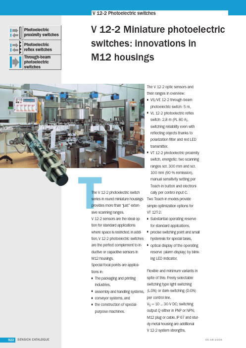
V 12-2Detecting objectson conveyor belts using VS/VE 12-2through-beam photo-electric switches.▼VL 12-2 photoelectric reflex switches canalso be used for the reliable detection of reflective surfaces, for example film-wrapped cardboard boxes.VT 12-2 photo-electric proximity switches used to ensure that waste is rolled up correctly when paper and film strips are cut.Is an objectpresent or not? The VT 12-2 photo-electric proximity switch provides the answer.▼▲▲VT 12T-2, Scanning distance 115 mm/340 mm115 mm Scanning distance340 mm Scanning distance 0 (mm)204060801001207025501152100210 (mm)501001502002503003502180200034023002112Scanning distance on white, 90 % remission Scanning distance on grey, 18 % remissionOperating distance Scanning distance, max. typical(mm)50100150200250300100101O p e r a t i n g r e s e r v eScanning distance max. typical Operating distanceVT 12(T)-2300 mm12(mm)10060802040100110O p e r a t i n g r e s e r v eOperating distance 21Scanning distance max. typical VT 12(T)-2100 mmScanning distance, max. typical 1)0... 115 mm 0 ... 340 mm Operating distance 1)2... 100 mm 2 ... 300 mmSensitivity setting Manual, per Teach-in buttonElectronic, per control input C (0 V)2)Light source 3), light type LED, infrared lightLight spot diameterApprox. 20 mm at 100 mm Approx. 28 mm at 300 mm Angle of dispersion of senderApprox. 11.4°(SD = max.), Approx. 22.6°(SD = 1/2 max.)Approx. 5.3°(SD = max.),Approx. 11.2°(SD = 1/2 max.)Supply voltage V S 10 ... 30 V DC 4)Ripple 5)≤10%Current consumption 6)≤20 mA Switching outputs Q: PNP Q: NPN Output current l A max.≤100 mASwitching mode Light-/Dark-switching selectable 2)Response time 7)≤1.25 ms Switching frequency max.8)400/sConnection typesCable 9)PVC, 2 m, 4 x 0.14 mm 2, Ø 3.75 mm PlugM12, 4-pinVDE protection class 10)VCircuit protection 11)A, B, C, D Enclosure ratingIP 67Ambient temperature T A Operation –25 °C ... +70 °C Storage –25 °C ... +70 °C WeightWith cable Approx. 54 g With plug Approx. 18 gHousing materialHousing:Nickel-coated brass/PA Optics:PC1)Object to be detected with 90%remission (relating to standard white in acc. with DIN 5033); 100 x 100 mm2)Controll input C – L.ON/D.ON and – external Teach-inC = open: light-switching L.ON C = + V S : dark-switching D.ONC = 0 V: Sensitivity setting per “externalTeach-in” active3)Average service life 100,000 h at T A = +25°C 4)Limit values5)May not exceed or fall short of V S tolerances 6)Without load7)Signal transit time with resistive load8)With light/dark ratio 1:19)Do not bend below 0°C 10)Reference voltage 50 V DC11)A =V Sconnections reverse-polarityprotectedB =Inputs and output reverse-polarityprotectedC =Interference pulse suppressionD =Outputs overload and short-circuitprotectedTechnical dataVT 12T-2P 112P 410N 112N 410P 132P 430N 132N 430TypeOrder no.VT 12T -2P 112 6 026 211VT 12T -2P 410 6 026 212VT 12T -2N 112 6 026 209VT 12T -2N 410 6 026 210VT 12T -2P 132 6 026 215VT 12T -2P 430 6 026 216VT 12T -2N 132 6 026 213VT 12T -2N 4306 026 214Order information0 (m)0.5 1.0 1.5 2.0 2.5 3.0Operating range Scanning range, max. typical0 2.50.03 2.00 2.30.03 1.80.90.10.7 2.80.03 2.323410.1 ... 0.7 mReflective tape Diamond GradePL 50 A/PL 40 A/P 25040.03 ... 1.8 m 3 C 1100.03 ... 2.0 m 2PL 80 A 0.03 ... 2.3 m1Reflector type Operating range VL 12-210001001011.01.52.02.50.5(m)O p e r a t i n g r a n g eOperating rangeReflectorC 110Scanning range, max. typical V L 12-22Scanning range, max.typ./reflector 0.03... 2.8 m/PL 80 A Operating range 0.03... 2.3 m/PL 80 A Sensitivity settingNot availableLight source 1), light type LED, red light, with polarization filter Light spot diameterApprox. 80 mm at 2 m Angle of dispersion of sender Approx. 2.3°(SR = max.), Approx. 6.3°(SR = 1/2 max.)Supply voltage V S 10 … 30 V DC 2)Ripple 3)≤10%Current consumption 4)≤20 mASwitching outputsQ: PNP Q: NPN Output current l A max.≤100 mASwitching mode Light-/Dark-switching selectable 5)Response time 6)≤1.25 ms Switching frequency max.7)400/sConnection types Cable 8)PVC, 2 m, 4 x 0.14 mm 2, Ø 3.75 mm PlugM12, 4-pinVDE protection class 9)VCircuit protection 10)A, B, C, D Enclosure ratingIP 67Ambient temperature T A Operation –25 °C ... +70 °C Storage –25 °C ... +70 °CWeightWith cable Approx. 54 g With plug Approx. 18 gHousing materialHousing: Nickel-coated brass/PA Optics: PC1)Average service life 100,000 h at T A = +25°C 2)Limit values3)May not exceed or fall short of V S tolerances 4)Without load5)L/D switching type control line L/D =open (not assigned)dark-switching D.ONL/D =+ V S : light-switching L.ON L/D =0 V: dark-switching D.ON6)Signal transit time with resistive load 7)With light/dark ratio 1:18)Do not bend below 0°C 9)Reference voltage 50 V DC10)A =V S connections reverse-polarityprotectedB =Inputs and output reverse-polarityprotectedC =Interference pulse suppressionD =Outputs overload and short-circuitprotectedTechnical dataVL 12-2P 132P 430N 132N 430Scanning range and operating reserveType Order no.VL 12-2P 132 6 026 219VL 12-2P 430 6 026 220VL 12-2N 132 6 026 217VL 12-2N 4306 026 218Order informationVS/VE 12-2100010010123451(m)O p e r a t i n g r e s e r v eOperating rangeScanning range, max. typical V S/V E 12-20 (m) 1.0 2.0 3.0 4.0 5.0 6.0Operating range Scanning range, max. typical5.04.0Scanning range, m a x .t yp .0... 5.0 m O p e r at in g r a n ge 0... 4.0 m Se n s i t ivi t y sett in gN ot a v a il a bl e Light source 1), light type L ED, infr a r e d li g h tLi g h t s p ot di a m ete rAppr o x . 100 mm at 4 m An g l e o f di s p e r s i o n o f se nd e r Appr o x . 1.4°(S R = m a x .), An g l e o f di s p e r s i o n o f r ece iv e r Appr o x . 4.5°(S R = 1/2 m a x .)Supply voltage V S 10 … 30 V DC 2)Rippl e 3)≤10%C urr e n t co n s ump t i o n 4)≤20 mASwitching outputs Q : PNP Q : NPN O u t pu t c urr e n t l A m a x .≤100 mAS wi tc hin g m o d e Li g h t-/Da rk -s wi tc hin g se l ecta bl e 5)R es p o n se t im e 6)≤2.0 m s S wi tc hin g fr e qu e n c y m a x .7)250/sConnection typesCa bl e 8) se nd e r V S 12-2 PV C, 2 m , 2 x 0.14 mm 2, Ø 3.75 mm Ca bl e 8) r ece iv e r V E 12-2 PV C, 2 m , 4 x 0.14 mm 2, Ø 3.75 mm Plu gM12, 4-pinVDE protection class 9)VCircuit protection 10)A , B, C, D Enclosure ratingIP 67Ambient temperature T A O p e r at i o n –25 °C ... +70 °C Sto r age –25 °C ... +70 °C WeightWi t h ca bl e V S a nd V E eac h a ppr o x . 54 g Wi t h plu g V S a nd V E eac h a ppr o x . 18 g Housing materialH o u s in g : Ni c k e l -coate d br ass /PA O p t i cs :P C1)Av e r age se rvi ce lif e 100,000 h at T A = +25°C 2)Limi t v a lu es3)M a y n ot e x cee d o r f a ll s h o r t o f V S to l e r a n ces 4)Wi t h o u t l oa d5)L/D s wi tc hin g t yp e co n t r o l lin e L/D =o p e n (n ot ass i g n e d)d a rk -s wi tc hin g D.O NL/D =+ V S : li g h t-s wi tc hin g L .O N L/D =0 V: d a rk -s wi tc hin g D.O N6)S i g n a l t r a n s i t t im e wi t h r es i st iv e l oa d 7)Wi t h li g h t /d a rk r at i o 1:18)Do n ot b e nd b e l o w 0°C 9)R e f e r e n ce v o l tage 50 V DC10)A =V S co nn ect i o n s r e v e r se-p o l a ri t ypr otecte dB =Inpu ts a nd o u t pu t r e v e r se-p o l a ri t ypr otecte dC =In te rf e r e n ce pul se s uppr ess i o nD =O u t pu ts o v e rl oa d a nd s h o r t-c ir c ui tpr otecte d11)Th e o rd e r n o. co n ta in s t r a n s mi tte r a nd r ece iv e r (= p a ir).Technical dataV S /V E 12-2P 132P 430N 132N 430Scanning range and operating reserveType 11)Order no.11)V S /V E 12-2P 132 6 026 223V S /V E 12-2P 430 6 026 224V S /V E 12-2N 132 6 026 221V S /V E 12-2N 4306 026 222Order information。


芯片esd等级标识全文共四篇示例,供读者参考第一篇示例:芯片的ESD等级标识是指芯片的静电放电(ESD)保护级别,用于表明芯片对静电放电的抗性能力。
ESD是指静电放电,是由人体或其它物质通过接触、摩擦、分离等方式积累电荷,然后在与其它物体接触时放电的现象。
静电放电对芯片的损坏可能导致芯片性能的下降、故障以及永久性损坏。
为了保护芯片不受静电放电的损害,生产厂商会在芯片上标识相应的ESD等级。
芯片的ESD等级标识通常通过符号或者文字来表示,以便用户能够快速了解芯片的静电放电保护等级。
目前国际上普遍采用JESD22-A114标准对芯片的ESD等级进行分类。
根据该标准,芯片的ESD等级可以分为以下几个等级:1. Human Body Model (HBM):人体模型下的ESD等级,表示芯片在人体模型下的ESD保护级别。
HBM是一种最简单的ESD模型,用来模拟人体对芯片的静电放电情况。
HBM等级通常通过符号HBM xKV来表示,其中x为ESD保护等级的电压值。
对于不同的芯片类型和用途,ESD等级的要求可能会有所不同。
通常情况下,用户在选择芯片时应根据自身的应用环境和使用需求来选取符合要求的ESD等级的芯片。
一般来说,ESD等级越高的芯片对静电放电的抗性能力越强,能够更好地保护芯片不受静电放电的损害。
芯片的ESD等级标识是非常重要的,它能够帮助用户快速了解芯片的静电放电保护性能,以便选择适合自己需求的芯片。
在平时使用和处理芯片时,用户也应当注意避免产生静电放电,以免对芯片造成不必要的损害。
【结束】。
第二篇示例:芯片的ESD(静电放电)等级标识对于电子产品的设计和生产至关重要。
ESD是指在两个物体接触或者分离时,由于静电产生的放电现象。
在芯片的设计和制造过程中,ESD等级标识起着至关重要的作用,它能够为用户提供保护,确保电子产品的可靠性和稳定性。
ESD等级标识主要用于表明芯片的抗静电性能等级。
通常情况下,芯片的ESD等级标识是通过数字或者字母来表示的,不同的等级代表着不同的防护能力。