RTL8019AS,RTL8029AS如何读写网卡的RAM
- 格式:doc
- 大小:274.00 KB
- 文档页数:8

![10M以太网接入处理芯片[RTL8029AS]详细技术手册](https://img.taocdn.com/s1/m/1762e0eae009581b6bd9eb23.png)
RTL8029ASRealtek PCI Full-Duplex Ethernet Controller with built-in SRAM ADVANCE INFORMATIONREALTEK SEMI-CONDUCTOR CO., LTD.HEAD OFFICE1F, NO. 11, INDUSTRY E. RD. IX, SCIENCE-BASEDINDUSTRIAL PARK, HSINCHU 30077, TAIWAN, R.O.C.TEL:886-3-5780211 FAX:886-3-5776047OFFICE3F, NO. 56, WU-KUNG 6 RD.,TAIPEI HSIEN, TAIWAN, R.O.C.TEL: 886-2-2980098 FAX: 886-2-2980094, 29800971. FEATURES (4)2. GENERAL DESCRIPTION (5)3. PIN CONFIGURATION (6)4. PIN DESCRIPTIONS (7)4.1. S IGNAL T YPE D EFINITION (7)4.2. P OWER P INS (7)4.3. PCI B US I NTERFACE P INS (7)4.4. M EMORY I NTERFACE P INS (INCLUDING BROM, EEPROM) (8)4.5. M EDIUM I NTERFACE P INS (9)4.6. LED O UTPUT P INS (9)5. REGISTER DESCRIPTIONS (10)5.1. G ROUP 1: NE2000 R EGISTERS (10)5.1.1. Register Table (10)5.1.2. Register Functions (12)5.1.2.1. NE2000 Compatible Registers (12)CR: Command Register (00H; Type=R/W) (12)ISR: Interrupt Status Register (07H; Type=R/W in Page0) (13)IMR: Interrupt Mask Register (0FH; Type=W in Page0, Type=R in Page2) (14)DCR: Data Configuration Register (0EH; Type=W in Page0, Type=R in Page2) (14)TCR: Transmit Configuration Register (0DH; Type=W in Page0, Type=R in Page2) (14)TSR: Transmit Status Register (04H; Type=R in Page0) (15)RCR: Receive Configuration Register (0CH; Type=W in Page0, Type=R in Page2) (15)RSR: Receive Status Register (0CH; Type=R in Page0) (15)CLDA0,1: Current Local DMA Registers (01H & 02H; Type=R in Page0) (16)PSTART: Page Start Register (01H; Type=W in Page0, Type=R in Page 2) (16)PSTOP: Page Stop Register (02H; Type=W in Page0, Type=R in Page2) (16)BNRY: Boundary Register (03H; Type=R/W in Page0) (16)TPSR: Transmit Page Start Register (04H; Type=W in Page0) (16)TBCR0,1: Transmit Byte Count Registers (05H & 06H; Type=W in Page0) (16)NCR: Number of Collisions Register (05H; Type=R in Page0) (16)FIFO: First In First Out Register (06H; Type=R in Page0) (16)CRDA0,1: Current Remote DMA Address registers (08H & 09H; Type=R in Page0) (16)RSAR0,1: Remote Start Address Registers (08H & 09H; Type=W in Page0) (16)RBCR0,1: Remote Byte Count Registers (0AH & 0BH; Type=W in Page0) (16)CNTR0: Frame Alignment Error Tally Counter Register (0DH; Type=R in Page0) (16)CNTR1: CRC Error Tally Counter Register (0EH; Type=R in Page0) (17)CNTR2: Missed Packet Tally Counter Register (0FH; Type=R in Page0) (17)PAR0-5: Physical Address Registers (01H - 06H; Type=R/W in Page1) (17)CURR: Current Page Register (07H; Type=R/W in Page1) (17)MAR0-7: Multicast Address Register (08H - 0FH; Type=R/W in Page1) (17)5.1.2.2. RTL8029AS Defined Registers (17)9346CR: 9346 Command Register (01H; Type=R/W except Bit0=R) (18)CONFIG0: RTL8029AS Configuration Register 0 (03H; Type=R) (18)CONFIG1: Reserved (18)CONFIG2: RTL8029AS Configuration Register 2 (05H; Type=R except Bit[7:5]=R/W) (18)CONFIG3: RTL8029AS Configuration Register 3 (06H; Type=R except Bit[6,2:1]=R/W) (19)HLTCLK: Halt Clock Register (09H; Type=W) (20)8029ASID0,1: RTL8029AS ID = 8029H (0E, 0FH; Type=R) (20)5.2. G ROUP 2: PCI C ONFIGURATION S PACE R EGISTERS (20)5.2.1. PCI Configuration Space Table (20)5.2.2. PCI Configuration Space functions (21)VID: Vendor ID Register (01-00H; Type=R) (21)DID: Device ID Register (03-02H; Type=R) (21)RID: Revision ID Register (08H; Type=R) (22)Command: Command Register (05-04H; Type=R except Bit1, 0=R/W) (22)Status: Status Register (07-06H; Type=R) (22)PIFR: Programming InterFace Register (09H; Type=R) (23)SCR: Sub-Class Register (0AH; Type=R) (23)BCR: Base-Class Register (0BH; Type=R) (23)HTR: Header Type Register (0EH; Type=R) (23)LTR: Latency Timer Register (0DH; Type=R) (23)BAR: Base Address Register (13-10H; Type=R/W except Bit4-0=R) (23)SVID: Subsystem Vendor ID Register (2C-2DH; Type=R) (23)SID: Subsystem ID Register (2E-2FH; Type=R) (24)BROMBAR: Boot ROM Base Address Register (33-30H; Type=R/W except Bit12-1=R) (24)ILR: Interrupt Line Register (3CH; Type=R/W) (24)IPR: Interrupt Pin Register (3DH; Type=R) (24)6. FUNCTION DESCRIPTION (25)6.1. RTL8029AS C ONFIGURATION P ROCESS (25)6.2. 9346 C ONTENTS (26)6.2.1 Detail values of 9346 CONFIG2-3 & 8029ASID0-1 bytes (26)6.2.2 ID PROM Contents (27)6.3. L OCAL M EMORY B US C ONTROL (28)6.4. F LOW C ONTROL (28)6.4.1. Control Frame Transmission (28)6.4.2. Control Frame Reception (28)6.5. LED B EHAVIORS (29)6.5.1 LED_TX: Tx LED (29)6.5.2 LED_RX: Rx LED (29)6.5.3 LED_CRS=LED_TX+LED_RX: Carrier Sense LED (30)6.5.4 LED_COL: Collision LED (30)6.5.5 LED Output States in Power Down Modes (31)6.6. L OOPBACK D IAGNOSTIC O PERATION (31)6.6.1. Loopback operation (31)(1) CRC enabled (CRC bit in TCR=0) (32)(2) CRC disabled (CRC bit in TCR=1) (32)6.6.2. To Implement Loopback Test (32)(1) To verify the integrity of data path (32)(2) To verify CRC logic (32)(3) To verify the address recognition function (33)(4) To Test Cable Connection (33)7. ELECTRICAL SPECIFICATIONS AND TIMINGS (35)7.1. A BSOLUTE M AXIMUM R ATINGS (35)7.2. D.C. C HARACTERISTICS (T C=0¢J TO 70¢J, V CC=5V+5%) (35)7.3. A.C. T IMING C HARACTERISTICS (35)7.3.1. PCI Configuration Read/Write (35)7.3.1.1. Configuration Read (36)7.3.1.2. Configuration Write (36)7.3.2. PCI I/O Read/Write (37)7.3.2.1. PCI I/O Read (37)7.3.2.2. PCI I/O Write (37)7.3.4. Output Timing for PCI Interface (38)7.3.5. Input Timing for PCI Interface (38)7.3.6. Serial EEPROM (9346) Auto-load (39)1. FEATURESm100-pin PQFP¯Pin-to-pin compatible with RTL8029¯16K byte SRAM built in¯Compliance to PCI V2.1¯Programmable PCI Vendor ID and Sub Vendor IDm PCI local bus single-chip Ethernet controllerm Compliant to Ethernet II and IEEE802.3 10Base5, 10Base2, 10BaseTm Supports Full-Duplex Ethernet function to double channel bandwidth¯Support Flow Control(802.3x) to improve network performance in full-duplex modem Supports three level power down modes:- Sleep- Power down with internal clock running- Power down with internal clock haltedm Built-in data prefetch function to improve performancem Built-in 10BaseT transceiverm Provides auto-detect capability between integrated 10BaseT transceiver and Attachment Unit Interface (AUI)m Supports auto polarity correction for 10BaseTm Supports Boot ROM function for PCI busm Supports 8K, 16K and 32K Boot ROM sizem Use 9346 (64*16-bit EEPROM) to store resource configurations and ID parametersm Capable of programming blank 9346 on board for manufacturing conveniencem Supports 4 diagnostic LED pins with programmable outputsP.S. “¯” denotes new feature of RTL8029AS2. GENERAL DESCRIPTIONThe RTL8029AS controller is an NE2000 compatible Ethernet Controller for PCI interface. Taking the benefit of PCI's high throughput rate, the RTL8029AS controller offers a 32-bit data path to highly improve the data transfer rate compared with traditional Ethernet card on ISA, EISA and MCA bus. Due to the additional benefits of PCI, the RTL8029AS controller provides a low maintaining cost network environment without usage barriers. The Auto-configuration function of PCI can relieve the users from pains of taking care the system resource conflict. The RTL8029AS controller also supports full-duplex and power down features. With three levels power down control features, the RTL8029AS controller is made to be an ideal choice of the network device for a GREEN PCI PC system. The full-duplex function enables simultaneously transmission and reception on the twisted-pair link to a full-duplex Ethernet switching hub. This feature not only increases the channel bandwidth from 10 to 20 Mbps but also avoids the performance degrading problem due to the channel contention characteristics of the Ethernet CSMA/CD protocol.The RTL8029AS controller requires no glue logic and integrates with Manchester Encoder/Decoder and 10BaseT transceiver on chip. The built-in 10BaseT transceiver can automatically correct the polarity error on its receiving pair. The RTL8029AS controller also has the capability of auto-sensing for 10Base2 or 10BaseT connection. Four diagnostic LEDs supported by RTL8029AS controller simplify the troubleshooting procedure in a network. Furthermore, The RTL8029AS controller supports 8K, 16K & 32K byte Boot ROM. It can be applied in a workstation without disk to improve the network security and management convenience. Data prefetch function in RTL8029AS controller can enhance the data transmission and highly uplift the network performance without extra fee.3. PIN CONFIGURATION4. PIN DESCRIPTIONS4.1. Signal Type DefinitionP Power pins include VDD and GND.I Input is a standard input-only signal.O It indicates output signal.T/S Tri-State is a bi-directional, tri-state input/output pin.S/T/S Sustained Tri-State is an active low tri-state signal owned and driven by one and only one agent at a time. The agent that drives an S/T/S pin low must drive it highfor at least one clock before letting it float.O/D Open Drain allowed multiple device to share as a wire-OR.4.2. Power Pins Type Description 22, 39, 52,75, 85, 100VDD P+5V DC power11, 17, 34,48, 72, 80,91GND P Ground4.3. PCI Bus Interface Pins Type Descriptions90CLK I Bus Clock provides timing for all transactions on PCI andis an input pin to every PCI device. All bus signals aresampled on the rising edge of CLK and all parameters aredefined with respect to this edge.92-99, 3-10, 20, 21, 23-28, 30-33, 35-38AD31-0T/S Address/Data are multiplexed on the same PCI pins. A bustransaction consists of an address phase followed by one ormore data phases. The address phase is the clock cycle inwhich FRAMEB is asserted. During data phase AD7-0contain the least significant byte(lsb) and AD31-24 containthe most significant byte(msb). Write data is stable andvalid when IRDYB is asserted and read data is stable andvalid when TRDYB is asserted.1, 12, 19,29CBE3-0B T/S Bus Command/Byte Enables are multiplexed on the samePCI pins. During the address phase of a transaction, CBE3-0B define the Bus Command. During the data phase CBE3-0B are used as Byte Enables. The Byte Enables definewhich physical byte lanes carry meaning data. CBE0Bapplies to byte 0(lsb) and CBE3B applies to byte 3(msb).18PAR T/S Parity is even parity across AD31-0 and CBE3-0B. PAR isstable and valid one clock after the address phase. For dataphases PAR is stable and valid one clock after eitherIRDYB is asserted on a write transaction or TRDYB isasserted on a read transaction.13FRAMEB S/T/S Cycle Frame is driven by the current master to indicate thebeginning and duration of an access. FRAMEB is assertedto indicate a bus transaction is beginning. While FRAMEBis asserted, data transfers continue. When FRAMEB isdeasserted, the transaction is in the final data phase.14IRDYB S/T/S Initiator Ready indicates the initiating agent's ability tocomplete the current data phase of the transaction. IRDYBis used in conjunction with TRDYB. A data phase iscompleted on any clock when both IRDYB and TRDYB areasserted. During a write, IRDYB indicates that valid data ispresent on AD31-0. During a read, it indicates the master isprepare to accept data. Wait cycles are inserted until bothIRDYB and TRDYB are asserted simultaneously.15TRDYB S/T/S Target Ready indicates the target's agent's ability tocomplete the current data phase of the transaction. TRDYBis used in conjunction with IRDYB. A data phase iscompleted on any clock when both TRDYB and IRDYB areasserted. During a read, TRDYB indicates that valid data ispresent on AD31-0. During a write, it indicates the target isprepare to accept data. Wait cycles are inserted until bothIRDYB and TRDYB are asserted simultaneously.16DEVSELB S/T/S Device Select, when actively driven, indicates the drivingdevice has decoded its address as the target of the currentaccess. As an input, DEVSELB indicates whether anydevice on the bus has been selected.2IDSEL I Initialization Device Select is used as a chip select forRTL8029AS controller during configuration read and writetransaction.89RSTB I When RSTB is asserted low, the RTL8029AS performs aninternal system hardware reset. RSTB must be held for aminimum of 120 ns periods. RSTB may be asynchronous toCLK when asserted or deasserted. It is recommended thatthe deassertion be synchronous to guarantee clean andbounce free edge.88INTAB O/D Interrupt A is an asynchronous attention signal which isused to request an interrupt.4.4. Memory Interface Pins (including BROM, EEPROM) Type Description49BOEB O Boot ROM chip select. Active low signal, asserted whenBoot ROM is read.50NC-Unused53EECS O9346 chip select. Active high signal, asserted when 9346 isread/write.51, 67-54MA14-0O Boot ROM address bus[57][EESK]O9346 serial data clock[56][EEDI]O9346 serial data input[55][EEDO]I9346 serial data output40-47MD7-0I/O Boot ROM data bus4.5. Medium Interface Pins Type Description82, 81CD+,CD-I This AUI collision input pair carries the differentialcollision input signal from the MAU.84, 83RX+,RX-I This AUI receive input pair carries the differential receiveinput signal from the MAU.77, 76TX+,TX-O This AUI transmit output pair contains differential linedrivers which send Manchester encoded data to the MAU.These outputs are source followers and require 270 ohmpull-down resistors to GND.87, 86TPIN+,TPIN-I This TP input pair receives the 10 Mbits/s differentialManchester encoded data from the twisted-pair wire.73, 74TPOUT+,TPOUT-O This pair carries the differential TP transmit output. Theoutput Manchester encoded signals have been pre-distortedto prevent overcharge on the twisted-pair media and thusreduce jitters.78X1I20Mhz crystal or external oscillator input.79X2O Crystal feedback output. This output is used in crystalconnection only. It must be left open when X1 is driven withan external oscillator.4.6. LED Output Pins Type Description71LED_BNC O This pin goes high when RTL8029AS's medium type is setto 10Base2 mode or auto-detect mode with link test failure.Otherwise, this pin is low. This pin can be used to controlthe power of the DC converter for CX MAU and connectedto an LED to indicate the used medium type.70LED0O When LEDS0 bit (in CONFIG3 register of RTL8029ASPage3) is 0, this pin acts as LED_COL. When LEDS0=1, itacts as LED_LINK.69, 68LED1,LED2O When LEDS1 bit (in CONFIG3 register of RTL8029ASPage3) is 0, these 2 pins act as LED_RX & LED_TXrespectively. When LEDS1=1, these pins act as LED_CRS& MCSB. Please refer to section 6.5 for details of thelightening behavior of all LEDs.5. REGISTER DESCRIPTIONSThe registers in RTL8029AS controller can be roughly divided into two groups by their address and functions -- one for NE2000, the other for PCI Configuration Space.5.1. Group 1: NE2000 RegistersThis group includes 4 pages of registers which are selected by bit PS0 & PS1 in the CR register. Each page contains 16 registers. Besides those registers compatible with NE2000, the RTL8029AS controller defines some registers for software configuration and feature enhancement.5.1.1. Register TableNo (Hex)Page0Page1Page2Page3[R][W][R/W][R][R][W]00CR CR CR CR CR CR01CLDA0PSTART PAR0PSTART9346CR9346CR02CLDA1PSTOP PAR1PSTOP--03BNRY BNRY PAR2-CONFIG0-04TSR TPSR PAR3TPSR--05NCR TBCR0PAR4-CONFIG2CONFIG206FIFO TBCR1PAR5-CONFIG3CONFIG307ISR ISR CURR---08CRDA0RSAR0MAR0---09CRDA1RSAR1MAR1--HLTCLK0A8029ID0RBCR0MAR2---0B8029ID1RBCR1MAR3---0C RSR RCR MAR4RCR--0D CNTR0TCR MAR5TCR--0E CNTR1DCR MAR6DCR8029ASID0-0F CNTR2IMR MAR7IMR8029ASID1-10-17Remote DMA Port18-1F Reset PortNotes: "-" denotes reserved. Registers with names typed in bold italic format are RTL8029AS defined registers and are not supported in a standard NE2000 adapter.Page 0 (PS1=0, PS0=0) Type Bit 7Bit 6Bit 5Bit 4Bit 3Bit 2Bit 1Bit 0 00H CR R/W PS1PS0RD2RD1RD0TXP STA STP 01H CLDA0R A7A6A5A4A3A2A1A0 PSTART W A15A14A13A12A11A10A9A8 02H CLDA1R A15A14A13A12A11A10A9A8 PSTOP W A15A14A13A12A11A10A9A8 03H BNRY R/W A15A14A13A12A11A10A9A8 04H TSR R OWC CDH0CRS ABT COL-PTX TPSR W A15A14A13A12A11A10A9A8 05H NCR R0000NC3NC2NC1NC0 TBCR0W TBC7TBC6TBC5TBC4TBC3TBC2TBC1TBC0 06H FIFO R D7D6D5D4D3D2D1D0 TBCR1W TBC15TBC14TBC13TBC12TBC11TBC10TBC9TBC8 07H ISR R/W RST RDC CNT OVW TXE RXE PTX PRX 08H CRDA0R A7A6A5A4A3A2A1A0 RSAR0W A7A6A5A4A3A2A1A0 09H CRDA1R A15A14A13A12A11A10A9A8 RSAR1W A15A14A13A12A11A10A9A8 0AH8029ID0R01010000 RBCR0W RBC7RBC6RBC5RBC4RBC3RBC2RBC1RBC0 0BH8029ID1R01000011 RBCR1W RBC15RBC14RBC13RBC12RBC11RBC10RBC9RBC8 0CH RSR R DFR DIS PHY MPA0FAE CRC PRX RCR W--MON PRO AM AB AR SEP 0DH CNTR0R CNT7CNT6CNT5CNT4CNT3CNT2CNT1CNT0 TCR W---OFST ATD LB1LB0CRC 0EH CNTR1R CNT7CNT6CNT5CNT4CNT3CNT2CNT1CNT0 DCR W-FT1FT0ARM LS LAS BOS WTS 0FH CNTR2R CNT7CNT6CNT5CNT4CNT3CNT2CNT1CNT0 IMR W-RDCE CNTE OVWE TXEE RXEE PTXE PRXE Page 1 (PS1=0, PS0=1) Type Bit 7Bit 6Bit 5Bit 4Bit 3Bit 2Bit 1Bit 0 00H CR R/W PS1PS0RD2RD1RD0TXP STA STP 01H PAR0R/W DA7DA6DA5DA4DA3DA2DA1DA0 02H PAR1R/W DA15DA14DA13DA12DA11DA10DA9DA8 03H PAR2R/W DA23DA22DA21DA20DA19DA18DA17DA16 04H PAR3R/W DA31DA30DA29DA28DA27DA26DA25DA24 05H PAR4R/W DA39DA38DA37DA36DA35DA34DA33DA32 06H PAR5R/W DA47DA46DA45DA44DA43DA42DA41DA40 07H CURR R/W A15A14A13A12A11A10A9A8 08H MAR0R/W FB7FB6FB5FB4FB3FB2FB1FB0 09H MAR1R/W FB15FB14FB13FB12FB11FB10FB9FB8 0AH MAR2R/W FB23FB22FB21FB20FB19FB18FB17FB16 0BH MAR3R/W FB31FB30FB29FB28FB27FB26FB25FB24 0CH MAR4R/W FB39FB38FB37FB36FB35FB34FB33FB32 0DH MAR5R/W FB47FB46FB45FB44FB43FB42FB41FB40 0EH MAR6R/W FB55FB54FB53FB52FB51FB50FB49FB48 0FH MAR7R/W FB63FB62FB61FB60FB59FB58FB57FB56Page 2(PS1=1, PS0=0) Type Bit 7Bit 6Bit 5Bit 4Bit 3Bit 2Bit 1Bit 000H CR R/W PS1PS0RD2RD1RD0TXP STA STP01H PSTART R A15A14A13A12A11A10A9A802H PSTOP R A15A14A13A12A11A10A9A803H-04H TPSR R A15A14A13A12A11A10A9A8 -05H|0BH0CH RCR R--MON PRO AM AB AR SEP0DH TCR R---OFST ATD LB1LB0CRC0EH DCR R-FT1FT0ARM LS LAS BOS WTS0FH IMR R-RDCE CNTE OVWE TXEE RXEE PTXE PRXE Page 3(PS1=1, PS0=1) Type Bit 7Bit 6Bit 5Bit 4Bit 3Bit 2Bit 1Bit 0 00H CR R/W PS1PS0RD2RD1RD0TXP STA STP 01H9346CR R EEM1EEM0--EECS EESK EEDI EEDOW EEM1EEM0--EECS EESK EEDI-02H-03H CONFIG0R-----BNC00 04H-05H CONFIG2R PL1PL0*FCE*PF--BS1BS0W*PL1PL0*FCE-----06H CONFIG3R-FUDUP LEDS1LEDS0-SLEEP PWRDN-W*-*FUDUP---SLEEP PWRDN-07H TEST1-Reserved08H--Unused09H HLTCLK W HLT7HLT6HLT5HLT4HLT3HLT2HLT1HLT0 0AH TEST2-Reserved0B-0DH--Unused*0EH8029ASID0R00101001*0FH8029ASID1R10000000 Notes: The registers marked with type='W*' can be written only if bits EEM1=EEM0=1.Notes: "*" denotes the bits or registers which are RTL8029AS defined bits or registers and are not supported in RTL8029.5.1.2. Register Functions5.1.2.1. NE2000 Compatible RegistersCR: Command Register (00H; Type=R/W)This register is used to select register pages, enable or disable remote DMA operation and issue commands.Bit Symbol Description7, 6PS1, PS0PS1PS0Register Page Remark000NE2000 compatible011NE2000 compatible102NE2000 compatible113RTL8029ASConfiguration5-3RD2-0RD2RD1RD0Function000Not allowed001Remote Read010Remote Write011Send Packet1**Abort/Complete remote DMA 2TXP This bit must be set to transmit a packet. It is internally reset either after thetransmission is completed or aborted. Writing a 0 has no effect.1STA The STA bit controls nothing. It only reflects the value written to this bit.POWER UP=0.0STP This bit is the STOP command. When it is set, no packets will be received ortransmitted. POWER UP=1.STA STP Function10Start Command01Stop CommandISR: Interrupt Status Register (07H; Type=R/W in Page0)This register reflects the NIC status. The host reads it to determine the cause of an interrupt.Individual bits are cleared by writing a "1" into the corresponding bit. It must be cleared after power up.Bit Symbol Description7RST This bit is set when NIC enters reset state and is cleared when a start command isissued to the CR. It is also set when receive buffer overflows and is cleared whenone or more packets have been read from the buffer.6RDC Set when remote DMA operation has been completed.5CNT Set when MSB of one or more of the network tally counters has been set.4OVW This bit is set when the receive buffer has been exhausted.3TXE Transmit error bit is set when a packet transmission is aborted due to excessivecollisions.2RXE This bit is set when a packet received with one or more of the following errors:- CRC error- Frame alignment error- Missed packet1PTX This bit indicates packet transmitted with no errors.0PRX This bit indicates packet received with no errors.IMR: Interrupt Mask Register (0FH; Type=W in Page0, Type=R in Page2)All bits correspond to the bits in the ISR register. POWER UP=all 0s. Setting individual bits will enable the corresponding interrupts.DCR: Data Configuration Register (0EH; Type=W in Page0, Type=R in Page2) Bit Symbol Description7-Always 16, 5FT1, FT0FIFO threshold select bit 1 and 0.4ARM Auto-initialize Remote0: Send Packet Command not executed.1: Send Packet Command executed.3LS Loopback Select0: Loopback mode selected. Bits 1 and 2 of the TCR must also be programmed forLoopback operation.1: Normal Operation2LAS This bit must be set to zero. NIC only supports dual 16-bit DMA mode.POWER UP =11BOS Byte Order Select0: MS byte placed on MD15-8 and LS byte on MD7-0. (32xxx,80x86)1: MS byte placed on MD7-0 and LS byte on MD15-8. (680x0)0WTS Word Transfer Select0: byte-wide DMA transfer1: word-wide DMA transferTCR: Transmit Configuration Register (0DH; Type=W in Page0, Type=R in Page2) Bit Symbol Description7-5-Always 1.4OFST Collision Offset Enable.3ATD Auto Transmit Disable.0: normal operation1: reception of multicast address hashing to bit 62 disables transmitter,reception of multicast address hashing to bit 63 enables transmitter.2, 1LB1, LB0LB1LB0Mode Remark000Normal Operation011Internal Loopback102External Loopback113External Loopback0CRC The NIC CRC logic comprises a CRC generator for transmitter and a CRCchecker for receiver. This bit controls the activity of the CRC logic. If this bit set,CRC is inhibited by transmitter. Otherwise CRC is appended by transmitter.Conditions CRC Logic ActivitiesCRC Bit Mode CRC Generator CRC Checker0normal enabled enabled1normal disabled enabled0loopback enabled disabled1loopback disabled enabledTSR: Transmit Status Register (04H; Type=R in Page0)This register indicates the status of a packet transmission.Bit Symbol Description7OWC Out of Window Collision. It is set when a collision is detected after a slot time(51.2us). Transmissions are rescheduled as in normal collisions.6CDH CD Heartbeat. The NIC watches for a collision signal (i.e., CD Heartbeat signal) during the first 6.4us of the interframe gap following a transmission. This bit isset if the transceiver fails to send this signal.5-Always 0.4CRS Carrier Sense lost bit is set when the carrier is lost during transmitting a packet.3ABT It indicates the NIC aborted the transmission because of excessive collisions.2COL It indicates the transmission collided with some other station on the network.1-Always 1.0PTX This bit indicates the transmission completes with no errors.RCR: Receive Configuration Register (0CH; Type=W in Page0, Type=R in Page2) Bit Symbol Description7, 6-Always 1.5MON When monitor mode bit is set, received packets are checked for address match, good CRC and frame alignment but not buffered to memory. Otherwise, packetswill be buffered to memory.4PRO If PRO=1, all packets with physical destination address accepted.If PRO=0, physical destination address must match the node address programmedin PAR0-5.3AM If AM=1, packets with multicast destination address are accepted.If AM=0, packets with multicast destination address are rejected.2AB If AB=1, packets with broadcast destination address are accepted.If AB=0, packets with broadcast destination address are rejected.1AR If AR=1, packets with length fewer than 64 bytes are accepted.If AR=0, packets with length fewer than 64 bytes are rejected.0SEP If SEP=1, packets with receive errors are accepted.If SEP=0, packets with receive errors are rejected.RSR: Receive Status Register (0CH; Type=R in Page0)Bit Symbol Description7DFR Deferring. Set when a carrier or a collision is detected.6DIS Receiver Disabled. When the NIC enters the monitor mode, this bit is set and receiver is disabled. Reset when receiver is enabled after leaving the monitormode.5PHY PHY bit is set when the received packet has a multicast or broadcast destination address. It is reset when the received packet has a physical destination address.4MPA Missed Packet bit is set when the incoming packet can not be accepted by NIC because of a lack of receive buffer or if NIC is in monitor mode. IncrementCNTR2 tally counter.3-Always 0.2FAE Frame Alignment Error bit reflects the incoming packet didn't end on a byte boundary and CRC did not match at last byte boundary. Increment CNTR0 tallycounter.1CRC CRC error bit reflects packet received with CRC error. This bit will also be setfor FAE errors. Increment CNTR1 tally counter.0PRX This bit indicates packet received with no errors.CLDA0,1: Current Local DMA Registers (01H & 02H; Type=R in Page0)These two registers can be read to get the current local DMA address.PSTART: Page Start Register (01H; Type=W in Page0, Type=R in Page 2)The Page Start register sets the start page address of the receive buffer ring.PSTOP: Page Stop Register (02H; Type=W in Page0, Type=R in Page2)The Page Stop register sets the stop page address of the receive buffer ring.BNRY: Boundary Register (03H; Type=R/W in Page0)This register is used to prevent overwrite of the receive buffer ring. It is typically used as a pointer indicating the last receive buffer page the host has read.TPSR: Transmit Page Start Register (04H; Type=W in Page0)This register sets the start page address of the packet to the transmitted.TBCR0,1: Transmit Byte Count Registers (05H & 06H; Type=W in Page0)These two registers set the byte counts of the packet to be transmitted.NCR: Number of Collisions Register (05H; Type=R in Page0)The register records the number of collisions a node experiences during a packet transmission.FIFO: First In First Out Register (06H; Type=R in Page0)This register allows the host to examine the contents of the FIFO after loopback.CRDA0,1: Current Remote DMA Address registers (08H & 09H; Type=R in Page0) These two registers contain the current address of remote DMA.RSAR0,1: Remote Start Address Registers (08H & 09H; Type=W in Page0)These two registers set the start address of remote DMA.RBCR0,1: Remote Byte Count Registers (0AH & 0BH; Type=W in Page0)These two registers set the data byte counts of remote DMA.CNTR0: Frame Alignment Error Tally Counter Register (0DH; Type=R in Page0)。


读卡流程
1、连接好读卡机与电脑(打开电脑和读卡机即可)
2、打开桌面上读卡.exe文件
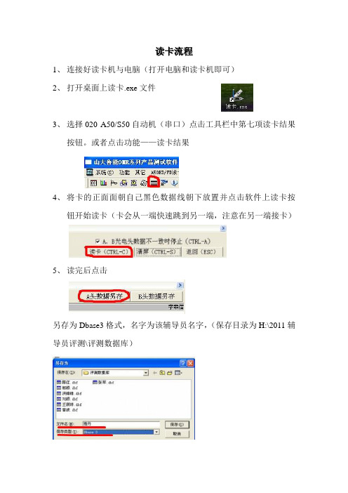
3、选择020 A50/S50自动机(串口)点击工具栏中第七项读卡结果
按钮。
或者点击功能——读卡结果
4、将卡的正面面朝自己黑色数据线朝下放置并点击软件上读卡按
钮开始读卡(卡会从一端快速跳到另一端,注意在另一端接卡)
5、读完后点击
另存为Dbase3格式,名字为该辅导员名字,(保存目录为H:\2011辅导员评测\评测数据库)
之后打开刚刚保存的Dbase3文件(以excel方式打开)将最上端DKCS 和DKNR
分别改为字段1和字段2
保存
在弹出的窗口选择“是”
然后直接关闭excel,在弹出的窗口选择“否”
6、打开H:\2011辅导员评测\PC.exe,(桌面上有快捷方式)
点击分析数据结果选择相应的辅导员数据,
点击统计,
统计结束后导出,把导出的excel表另存为H:\2011辅导员评测\数据分析。
注意事项
1、读卡时因为纸张潮湿或者其他原因可能会中断读卡,读卡中断后将有问题的卡取出并重新点击读卡来读其他的卡,最后将有问题的卡一起读。
2、读卡是辅导员评测中原始数据的录入,非常重要,大家务必要认
真对待,宁可读慢,不要读错,读完之后目测一下数据的准确性。
3、将读完的卡统一放在指定的箱子内
4、如读卡过程中有任何疑问询问老师或者白塔拉、汪晓龙、李帅、
鲁博、佀昊均可!。
嵌入式系统中常见的网卡驱动比较(CS8900A,RTL8019,DM9000)今天我又看了一些文章,想看看具体DM9000和CS8900A有什么区别?在KITL移植的时候,怎么样才能才能把CS8900A换成DM9000,因为我的KITL移植就卡在这里了,我的板子是DM9000驱动,我当然想在5.0到6.0的移植一步到位,可是在移植过程中由于是基于模拟器进行移植的,默认的是CS89 00A网卡驱动,导致KITL出错,具体怎么改呢?这是一个问题,先留在这里。
先把我今天看的一篇文章留在这里!1.CS8900ACS8900芯片是Cirrus Logic公司生产的一种局域网处理芯片,在嵌入式领域中使用非常常见。
它的封装是100-pin TQFP,内部集成了在片RA M、10BASE-T收发滤波器,并且提供8位和16位两种接口。
CS8900与ARM芯片按照16位方式连接,网卡芯片复位后默认工作方式为I/O连接,基址是300H。
CS8900A还提供其它性能和配置选择.它独特的Packet Page结构可自动适应网络通信量模式的改变和现有系统资源,从而提高系统效率。
MCU与CS8900A的数据传输有三种模式:I/O模式,存储器模式和DMA模式.本设计采用CS8900A默认的I/O模式,因为I/O模式简单易用. 在I/O模式下,通过访问8个16位的寄存器来访问PacketPage结构,这8个寄存器被映射到2410地址空间的16个连续地址。
当CS8900A上电后,寄存器默认的基址为0x300h。
电路连接如下:CS8900A的IO模式特点就是这个PacketPage结构,使用PacketP agePointer和PacketPageData Port这两个寄存器对CS8900A的内部寄存器进行配置,非常方便。
#define CS8900_PPTR *(volatileCS8900_REG*) (CS8900_BASE+0x05*CS8900_OFF)//PacketPagePointer的定义#define CS8900_PDATA *(volatile CS8900_REG *)(CS8900_BASE+0x06*CS8900_OFF)//PacketPageData Port通过如下函数对cs8900a设置get_reg(int regno) //32位模式,读寄存器的数据{CS8900_PPTR = regno; // regno为要读的寄存器偏移地址return (unsigned short) CS8900_PDATA; //返回要读寄存器的数据}static void put_reg(int regno, unsigned short val) //写寄存器{CS8900_PPTR = regno;CS8900_PDATA = val; //写寄存器}其中CS8900_BASE为基址与硬件连接有关。
RAM的一般结构和读写过程RAM(Random Access Memory)是计算机中的一种主要的存储设备,用于临时存储数据和指令。
它具有随机访问数据的能力,可以根据需要快速读取和写入数据。
RAM的一般结构和读写过程如下。
一般结构:RAM由一个或多个存储单元组成,每个存储单元由一个存储位组成,存储位可以存储一个二进制值(0或1)。
每个存储单元都有一个唯一的地址,用于访问和识别该单元。
存储单元可以按照不同的组织方式进行排列,常见的有随机存取存储器(Random Access Memory)、动态随机访问存储器(Dynamic Random Access Memory)和静态随机访问存储器(Static Random Access Memory)等。
读写过程:1.选择存储单元:首先,需要选择要读取或写入的特定存储单元。
这需要使用指定的地址来选择存储单元。
2.读取操作:当需要从RAM中读取数据时,计算机将根据所指定的地址发送一个读取信号。
这会导致特定存储单元中的数据被读取并被放置在RAM的输出线上。
然后,输出线上的数据可以由计算机的其他部分使用,如中央处理器(CPU)。
3.写入操作:当需要将数据写入RAM时,计算机将根据所指定的地址发送一个写入信号,并同时发送要写入的数据。
这会导致特定存储单元中的数据被更新为新的数据值。
4.刷新操作(仅适用于动态RAM):动态RAM需要定期进行刷新操作,以维持存储单元中的数据值。
这是因为动态RAM中的信息是通过电容器来存储的,电容器会逐渐失去电荷,导致数据丢失。
因此,动态RAM需要周期性地刷新,以重新充电并保持数据的正确性。
5.速度和延迟:RAM具有较快的读写速度,可以在几纳秒的时间内进行操作。
然而,RAM的速度也会受到一些因素的影响,如访问时间、数据传输速度和延迟。
延迟是指从发出指令到开始执行指令所需的时间,而数据传输速度则指数据从RAM传输到其他设备的速率。
总结:RAM的一般结构包括存储单元、地址和数据线等组件,用于临时存储数据和指令。
以太网控制芯片RTL8019AS 详细配置苏锦秀,杨庆江,张广璐(黑龙江科技学院 黑龙江哈尔滨 150027)摘 要:R TL8019AS 是目前实现设备接入以太网普遍采用的一种接口控制芯片,在实际应用中最重要的就是对芯片的配置。
为了使广大工程技术人员能够更好地应用该芯片,对R TL8019AS 工作在不同方式下的配置做了详细的说明解释,并总结了在应用中芯片工作在不同方式下的优缺点。
关键词:R TL8019AS ;跳线方式;非跳线方式;工作方式中图分类号:TP368.4 文献标识码:B 文章编号:10042373X (2007)222151203The Detailed Conf iguration of Ethernet Controlling Chip RT L8019ASSU Jinxiu ,YAN G Qingjiang ,ZHAN G Guanglu(Heilongjiang Institute of Science and Technology ,Harbin ,150027,China )Abstract :R TL8019AS is a kind of interface controlling chip which the equipments access to Ethernet in current.In the practical application ,the most important is the chip ′s configuration.In order to enable the general engineers and technicians u 2sing this chip better ,the article gives detailed configuration showing to the R TL8019AS which working under different styles.And summarizes the chip ′s strongpoint and shortcoming working in the different styles in the application.The article enables the general engineers and technicians understand the the chip ′s configuration better ,and provides certain instruction in prac 2tice.K eywords :R TL8019AS ;jumper ;jumperless ;working style收稿日期:2007204223 以太网控制芯片R TL8019AS 以其优良的性能、低兼的价格,在市场上10Mb/s 网卡中占有相当的比例。
RTL8029AS和RTL8019AS的内核其实是一样的,都是Ne2000兼容的寄存器结构,都有一样大小的ram,读取和操作的方法都是一样的.事实上对RTL8029AS的驱动是跟RTL8019AS一样的.没有很大的差别,因此很多关于RTL8029AS的论述也适用于RTL8019AS,同样对于RTL8019AS的论述,也适用于RTL8029AS.用户最好将我的关于RTL8019AS,RTL8029AS的文章都看一遍.RTL8019AS或RTL8029AS(简称为RTL8*19AS),RTL8*19AS有两块ram,一块16k字节的ram的地址为0x4000-0x7fff,一块32字节的ram的地址为0x0000-0x001f.存储是分页的,每256个字节称为一页.RAM地址:0x4000-0x40ff是一页,我们称该页为第0x40页(或页0x40),页码也就是16位地址的高8位.0x4100-0x41ff 是一页,称为第0x41页.0x0000-0x00ff 是一页,称为第0页.......第0页的内存又叫Prom.是Ne2000兼容的网卡都有的.Prom实际上只有32字节,从地址0x0000-0x0001F,其他地址0x0020-0x00ff存储的内容跟0x0000-0x001f是一样的,是重复的.地址0x0000-0x001f存储的内容:我们可以发现以太网地址被重复存储.主要是为了适应8位和16位的dma.(在16位的dma传输方式时,地址跟上面的定义不同.),我们一般使用8位的dma,一次传输一个字节,使用8条数据线.(而16位的dma是一次传输2个字节,需要16条数据线,适合使用16位的单片机或dsp).作为一个例子,在一块RTL8029AS网卡里读出的内容如下:0x0000-0x001f:52525454ABAB3D3D8E8E2C2C545446464C4C49494E4E40402222202 0575757570x0020-0x003f:52525454ABAB3D3D8E8E2C2C545446464C4C49494E4E40402222202 0575757570x0040-0x005f:52525454ABAB3D3D8E8E2C2C545446464C4C49494E4E40402222202 0575757570x0060-0x007f:52525454ABAB3D3D8E8E2C2C545446464C4C49494E4E40402222202 0575757570x0080-0x009f:52525454ABAB3D3D8E8E2C2C545446464C4C49494E4E40402222202 0575757570x00a0-0x00bf:52525454ABAB3D3D8E8E2C2C545446464C4C49494E4E40402222202 0575757570x00c0-0x00df:52525454ABAB3D3D8E8E2C2C545446464C4C49494E4E40402222202 0575757570x00e0-0x00ff:52525454ABAB3D3D8E8E2C2C545446464C4C49494E4E40402222202 057575757那么该网卡的地址是:5254AB3D8E2C,单地址和双地址的内容是重复的.一般使用偶数地址的内容.Prom是网卡在复位的时候从93C46里读出来的.如果你没有使用93C46,那么就不要使用Prom.那么如何获得网卡的地址,有两种方法,一是直接读93C46,二是读Prom.网卡在工作的时候的网卡地址是由寄存器MAR0,MAR1,MAR2,MAR3,MAR4,MAR5决定,而不是93C46,也不是Prom. 而这几个寄存器的内容需要用户自己编写程序写入.一般可以读出Prom里的网卡地址,然后写入到这6个寄存器里.如果你没有使用93C46,那么Prom也是不可以使用的,这时要由你的程序自己指定一个网卡地址, 网卡地址不能跟别的网卡地址相同,写入到MAR0-MAR5里.例如使MAR0=00MAR1=00MAR2=00MAR3=00MAR4=00MAR5=08那么网卡的地址就是:00:00:00:00:00:08所有发给00:00:00:00:00:08地址的数据包就可以被网卡收到.发送数据包的时候你的程序也要使用MAR0-MAR5的值作为发送的源地址.0x4000-0x7fff共16k字节的ram是网卡接收和发送数据包用的.该16k字节的ram实际上是双端口的ram,可以同时被网卡读/写和用户读/写,相互之间不影响,网卡读/写比用户读写的优先级高,举个例子:假如网卡收到一个数据包,需要放到0x5000开始的缓冲区,那么需要写入第0x50页.这时用户同时读取旧的数据包,该数据包放在0x4000开始的一段缓冲区,那么需要读第0x40页.网卡优先,它先写入一个字节,然后才读取一个字节到ISA总线上.内部总线的速度很快,是20Mhz,而ISA总线只有8Mhz, 网卡足够快进行同时读写数据,互不影响.。
要接收和发送数据包都必须读写网卡的内部的16k的ram,必须通过DMA进行读和写.网卡的内部ram是一块双端口的16k字节的ram.所谓双端口就是说有两套总线连结到该ram,一套总线A是网卡控制器读/写网卡上的ram,另一套总线B是单片机读/写网卡上的ram.总线A又叫Local DMA,总线B又叫Remote DMA.上图中虚线框住的部分为Remote DMA,也就是单片机对网卡ram进行读写的总线,对8019来说就是ISA总线.没有框住的部分(左边的部分),就是Local DMA,网卡控制器对网卡ram进行读写的总线.其中的地址总线没有画出来,只画了数据总线.实际在ram的内部还有一些总线仲裁的逻辑,这里也没有画出来.所谓总线仲裁的逻辑就是为了实现两套总线都能进行对ram的读写,而不互相冲突.网卡控制器读写网卡ram(Local DMA)的优先级比单片机读写网卡ram的优先级要高.优先级要高的意思是:1.当两者都要请求控制总线时.Local DMA优先获得控制权.2.高优先级的Local DMA可以中断Remote DMA,而Remote DMA不能中断Local DMA3.在Remote DMA,也就是单片机对网卡ram读写的过程进行中可以被Local DMA 中断,Local DMA中断Remote DMA,然后进行Local DMA的数据传输,Local DMA传输完毕之后继续刚才被中断的Remote DMA,以完成Remote DMA的传输.上图中的Remote就是Remote DMA的传输,Local burst就是Local DMA的传输.图的左边是一个Remote DMA被Local DMA中断的示意图.Remote DMA是等到Local Burst完成之后才结束该次的传输.被打断多久的时间取决于FT1,FT0(是DCR配置寄存器的位)单片机的总线要比网卡的DMA总线慢很多.网卡的DMA总线大概在10Mhz,而单片机的总线大概1Mhz.所以在Remote DMA的过程中不需要特别的等待时序.但是如果使用较快的CPU,比如DSP,ARM等,可能要考虑时序问题.也就是说IOCHRDY(ISA总线的一个信号,RTL8019AS),或者TRDY(PCI总线的信号RTL8029AS) ,是需要考虑连到CPU上,或者做一定的处理.那么对于不快也不慢的AVR单片机来说,要不要接IOCHRDY?估计是要的.因为我不提供avr的上网方案,所以也没有做太多的研究.对于77E58来说可以不接IOCHRDY,因为77E58可以内部设置外部ram的存取的速度.DMA有8位和16位两种.网卡支持这两种DMA,一般我们使用8位的DMA,8位的DMA的接线比较少,同时适合单片机处理.电脑里一般使用16位DMA.有人问到在电脑里如何使用8位的DMA的问题.有些卡自动检测总线上的IOCS16B来选择总线,比如RTL8019as,我试过RTL8019as使用8位DMA在电脑里是失败的.如果真的要在电脑里使用8位的DMA,要把该引脚IOCS16B断开(可以割断),而不连到ISA总线上,这样这些网卡会自动的进行8位的操作(地址译码为10位).对于使用DM9008芯片的网卡,16位DMA传输是由SLOT引脚决定的。
我试过把DM9008的IOCS16B引脚与ISA槽断开(通过贴“透明胶”的方法),配套的设置程序检查时死机。
如果想DM9008使用8位DMA操作,应该把SLOT引脚割断,而不是IOCS16B。
在DSP里可以使用16位的DMA.因为不同的单片机(CPU),代码可能不同,我在下面将用几种表示法来论述: 假设用到的I/O地址为0xC000,读出到temp变量或写temp到寄存器,temp 为8位变量:通用的表达式:void write_register(unsigned char address,unsigned char value)或void write_register(unsigned int address,unsigned char value) unsigned char read_register(unsigned char address)或unsigned char read_register(unsigned int address)上面的表达式中,根据你的地址或寻址方法而选择unsigned int address或unsigned char address.上表给出了用c语言或汇编语言或其他语言的表达的等价的程序.下面给出用51单片机的c语言程序:#define reg00 XBYTE[0xc000] //reg00- 10为isa网卡接口的寄存器地址240-250;#define reg01 XBYTE[0xc100]#define reg02 XBYTE[0xc200]#define reg03 XBYTE[0xc300]#define reg04 XBYTE[0xc400]#define reg05 XBYTE[0xc500]#define reg06 XBYTE[0xc600]#define reg07 XBYTE[0xc700]#define reg08 XBYTE[0xc800]#define reg09 XBYTE[0xc900]#define reg0a XBYTE[0xca00]#define reg0b XBYTE[0xcb00]#define reg0c XBYTE[0xcc00]#define reg0d XBYTE[0xcd00]#define reg0e XBYTE[0xce00]#define reg0f XBYTE[0xcf00]#define reg10 XBYTE[0xd000]xdata unsigned char buffer[1536];//缓冲区,放在外部ram.unsigned int count;//需要读或写的字节数unsigned int i;//DCR=0xc8;要配置DCR为8位的dmavoid write_dma(unsigned int address,unsigned int count)//写网卡的ram {//address为要写入到网卡里的ram的起始地址,count为要连续写入的字节数page(0);reg09=address>>8;//address highreg08=address&0xff;//address lowreg0b=count>>8; //write count highreg0a=count&0xff;//write count lowreg00=0x12 ;//dma writefor(i=0;i<count;i++){reg10=buffer[i];}reg0b=0; // count high 中止DMA操作reg0a=0;// count lowreg00=0x22;//abort/complete dma page 0}执行的结果是将buffer数组的内容被写入到网卡的起始ram地址address的一段ram里.程序当中的最后3句:reg0b=0; // count highreg0a=0;// count lowreg00=0x22;//abort/complete dma page 0可以不要,但推荐使用,以便发生错误的时候能够正确的退出DMA传输,3句是中止DMA的代码.在电脑里死机是很"正常"的,而在单片机里"死机"是大事,所以要考虑更多,一旦时序配合有问题,DMA就可能发生错误,提供发生错误时的恢复是有必要的.void read_dma(unsigned int address,unsigned int count)//读网卡ram {//address为网卡里的ram的起始地址,count为要连续读取的字节数page(0);reg09=address>>8;//address highreg08=address&0xff;//address lowreg0b=count>>8; //write count highreg0a=count&0xff;//write count lowreg00=0x0a ;//dma readfor(i=0;i<count;i++){buffer[i]=reg10;}reg0b=0; // count high 中止DMA操作reg0a=0;// count lowreg00=0x22;//abort/complete dma page 0}执行的结果是将网卡里的起始地址为address的共count个字节读入到buffer[i]里.如果是使用模拟i/o,程序如下:unsigned char read_register(unsigned char address){//读寄存器unsigned char temp;ea=0;//关闭中断是推荐的p2=address;p0=0xff; //这句不能省略read=0;temp=p0;read=1;//read为单片机的读引脚ea=1;return(temp);}void write_register(unsigned char address,unsigned char value){//写寄存器ea=0;p2=address;p0=value;write=0;//write为单片机的写引脚write=1;p0=0xff; //这句也是需要的.ea=1;}那么我给出的read_dma,write_dma里的函数的i/o替换成模拟i/o的函数就可以了,举例如下:将#define reg10 0xd0reg10=buffer[i] ;替换为write_register(reg10,buffer[i]);buffer[i]=reg10 ;替换为buffer[i]=read_register(reg10);其他reg0a,reg0b等也是做类似的替换.建议不要使用模拟i/o,因为速度慢,同时也不可靠.模拟i/o中一般要关闭中断. 因为如果不关闭中断,会引起被中断,使读或写寄存器的时间变得很长.尽管DMA有优先级,但是如果read或write线一直处于低电平的时候,能否被Local DMA中断,我是持有疑问的. 网卡有8字节的FIFO,假设在单片机读写网卡ram的同时,网卡收到一个数据包,那么FIFO最多可以存储64个bit就必须启动Local DMA写网卡ram,网卡的速率为10,000,000bit/秒,64个bit的时间为6.4微秒. 单片机读写一个字节的网卡ram的时间最好不要超过6.4微秒.所以关闭中断以尽快执行i/o操作.虽然资料上没有说是否可以超过6.4微秒.有兴趣的可以做实验看是否一个很慢的read,write会不会影响网卡收数据包.有时候我们不要相信资料.比如有些单片机书对MOVX指令的时序图就有误.RTL8019AS关于溢出时网卡不会覆盖以前接收的数据包的论述也是有误的. "尽信书不如无书"."实践是检验真理的唯一标准".就像资料说DM9008说支持8位DMA一样,我以前在电脑里试过,怎么也不行,用单片机的时候就可以.网卡并不是为单片机设计的,有些在电脑里不会出现的问题在单片机里可能碰到.如果采用16位的dma(有些客户用dsp,或者在电脑里驱动,16位的dma要求有16条数据线的CPU,不能用在51单片机),那么也给出大家参考://DCR=0xC9;//配置成16位dma.unsigned int buffer[768];//注意用int的数组void write_dma(unsigned int address,unsigned int count)//写网卡的ram{//address为要写入到网卡里的ram的起始地址,count为要连续写入的字节数page(0);reg09=address>>8;//address highreg08=address&0xff;//address lowreg0b=count>>8; //write count highreg0a=count&0xff;//write count lowreg00=0x12 ;//dma writecount=(count+1) /2;for(i=0;i<count;i++){reg10=buffer[i];}reg0b=0; // count high 中止DMA操作reg0a=0;// count lowreg00=0x22;//abort/complete dma page 0}void read_dma(unsigned int address,unsigned int count)//读网卡ram {//address为网卡里的ram的起始地址,count为要连续读取的字节数page(0);reg09=address>>8;//address highreg08=address&0xff;//address lowreg0b=count>>8; //write count highreg0a=count&0xff;//write count lowreg00=0x0a ;//dma readcount=(count+1) /2;for(i=0;i<count;i++){buffer[i]=reg10;}reg0b=0; // count high 中止DMA操作reg0a=0;// count lowreg00=0x22;//abort/complete dma page 0}上面的count=(ount+1) /2,为什么要加一,是因为读取字节数为单数的时候就要.。