EL7242C中文资料
- 格式:pdf
- 大小:190.38 KB
- 文档页数:8

XC9572是XILINX公司生产的一款高性能可编程逻辑器件。
它内含4个36V18功能块,并具有1600个可用系统门。
其系统结构如图1所示。
从结构上看,XC9572包含三种单元,即宏单元、可编程I/O单元和可编程内部连线。
其主要特点如下:●所有可编程管脚间的脚对脚延时均为5ns;●系统的时钟速度可达到125MHz;●具有72个宏单元和1600个可用系统门;●可编程次数为10000次;●可采用5V在线编程和擦除;●拥有强大的管脚锁定能力;●每个宏单元都具有可编程低功耗模式;●未用的管脚有编程接地能力;●提供有编程保密位,可对设计提供加密保护以防止非法读取;●外部I/O引脚与3.3V和5V兼容。
2 HDB3的编解码及实现原理HDB3码(三阶高密度双极性码)是基带电信设备之间进行基带传输的主要码型之一。
它的主要特点是易于提取时钟、不受直流特性影响、具有自检能力、连令串小于3个等。
E1信号是我国和欧洲国家电信传输网一次群使用的传输系统。
E1信号由32个64kbps的PCM话路经过时分复用形成。
CCITT建议G.703标准详细规定了HDB3码用于E1信号的标准。
用XC9572实现E1信号的HDB3编解码电路比较简单,而且无需可调整外围电路。
本设计使用了PC44封装形式的XC9572可编程逻辑器件共有30个可编程IO引脚、6个电源引脚和4个JTAG引脚。
整个设计使用了XC9572器件80%的容量。
图2所示是其实现电路图。
HDB3码是AMI(AlternateMarkInversion)码的改进型。
AMI码是用交替极性的脉冲表示码元“1”,用无脉冲表示码元“0”。
为了防止电路长时间出现无脉冲状态,HDB3码的编码规则是:当没有4个或4个连续的“0”码时,就按AMI码规则编码;当出现4个或4个连续的“0”码时,每4个连续“0”的第一个“0”的变化应视它前面相邻的“1”的情况而定,如果它的前一个“1”的极性与前一个破坏点的极性相反而本身就是破坏点,则4个连续的“0”的第一个仍保持“0”;如果它的前一个“1”的极性与前一个破坏点的极性相同而本身就是破坏点,则第一个“0”改为“1”。
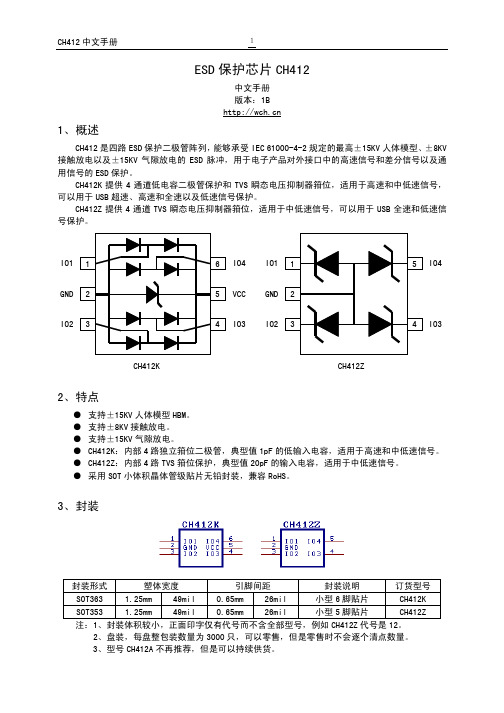
ESD 保护芯片CH412中文手册 版本:1B 1、概述CH412是四路ESD 保护二极管阵列,能够承受IEC 61000-4-2规定的最高±15KV 人体模型、±8KV 接触放电以及±15KV 气隙放电的ESD 脉冲,用于电子产品对外接口中的高速信号和差分信号以及通用信号的ESD 保护。
CH412K 提供4通道低电容二极管保护和TVS 瞬态电压抑制器箝位,适用于高速和中低速信号,可以用于USB 超速、高速和全速以及低速信号保护。
CH412Z 提供4通道TVS 瞬态电压抑制器箝位,适用于中低速信号,可以用于USB 全速和低速信号保护。
CH412K CH412Z2、特点● 支持±15KV 人体模型HBM 。
● 支持±8KV 接触放电。
● 支持±15KV 气隙放电。
● CH412K :内部4路独立箝位二极管,典型值1pF 的低输入电容,适用于高速和中低速信号。
● CH412Z :内部4路TVS 箝位保护,典型值20pF 的输入电容,适用于中低速信号。
● 采用SOT 小体积晶体管级贴片无铅封装,兼容RoHS 。
3、封装封装形式 塑体宽度 引脚间距 封装说明 订货型号 SOT363 1.25mm 49mil 0.65mm 26mil 小型6脚贴片 CH412K SOT353 1.25mm 49mil 0.65mm 26mil 小型5脚贴片 CH412Z 注:1、封装体积较小,正面印字仅有代号而不含全部型号,例如CH412Z 代号是12。
2、盘装,每盘整包装数量为3000只,可以零售,但是零售时不会逐个清点数量。
IO4 IO3 IO3 VCC IO44、型号CH412B已经停产,请换用CH412K,多出的两个通道可以悬空或并联(低速时)。
4、引脚CH412K 引脚号CH412Z引脚号引脚名称类型引脚说明2 2 GND 电源公共接地端,必须直接连接到全局地5 无VCC 电源正电源端,必须靠近引脚对GND连接0.1μF电容,用于USB信号保护时通常为3.3V(或者5V),用于其它信号须同被保护芯片的电源电压(2V~5V)1,3,4,6 1,3,4,5 IO1~IO4 信号ESD保护通道,与被保护芯片的信号引脚并联5、应用说明CH412设计用来与被保护芯片内置的ESD保护一起工作。

© 2000 Fairchild Semiconductor Corporation DS500192February 1999Revised July 200074VCX16722 Low Voltage 22-Bit Register with 3.6V Tolerant Inputs and Outputs74VCX16722Low Voltage 22-Bit Registerwith 3.6V Tolerant Inputs and OutputsGeneral DescriptionThe VCX16722 low voltage 22-bit register contains twenty-two non-inverting D-type flip-flops with 3-STATE outputs and is intended for bus oriented applications. The design has been optimized for use with JEDEC compliant 200 pin DIMM modules.The 74VCX16722 is designed for low voltage (1.65V to 3.6V) V CC applications with I/O capability up to 3.6V.The 74VCX16722 is fabricated with an advanced CMOS technology to achieve high speed operation while maintain-ing low CMOS power dissipation.Featuress 1.65V–3.6V V CC specifications provided s 3.6V tolerant inputs and outputs s t PD (CLK to O n )3.6ns max for 3.0V to 3.6V V CC4.6ns max for 2.3V to 2.7V V CC 9.2ns max for 1.65V to 1.95V V CCs Power-down high impedance inputs and outputs s Supports live insertion/withdrawal (Note 1)s Meets JEDEC registered module specifications s Static Drive (I OH /I OL )±24mA @ 3.0V ±18mA @ 2.3V ±6mA @ 1.65Vs Latchup performance exceeds 300 mA s ESD performance:Human body model > 2000V Machine model >200VNote 1: To ensure the high-impedance state during power up or power down, OE should be tied to V CC through a pull-up resistor; the minimum value of the resistor is determined by the current sourcing capability of the driver.Ordering Code:Devices also available in T ape and Reel. Specify by appending the suffix letter “X ” to the ordering code.Order Number Package NumberPackage Description74VCX16722MTDMTD6464-Lead Thin Shrink Small Outline Package (TSSOP), JEDEC MO-153, 6.1mm Wide 274V C X 16722Connection Diagram Pin DescriptionsTruth TableH = HIGH Voltage Level L = LOW Level VoltageX = Immaterial (HIGH or LOW, Inputs may not float)Z = High ImpedanceO 0 = Previous O 0 before LOW-to-HIGH transition of Clock = LOW-to-HIGH transitionFunctional DescriptionThe VCX16722 contains twenty-two D-type flip-flops with 3-STATE standard outputs. The twenty-two flip-flops will store the state of their individual D-type inputs that meet the setup and hold time requirements on the LOW-HIGH Clock (CLK) transition, when the Clock-Enable (CE) is LOW. The 3-STATE standard outputs are controlled by the Output-Enable (OE). When OE is HIGH, the standard out-puts are in high impedance mode but this does not inter-fere with entering new data into the flip-flops.Logic DiagramPin Names DescriptionOE Output Enable Input (Active LOW)CE Clock Enable Input (Active Low)CLK Clock Input D 1 - D 21Data Inputs O 1 - O 213-STATE OutputsCLK CE OE D 0-D 21O 0-O 21X X H X Z XH L X O 0 L L L L L L H H L or HLLXO 074VCX16722Absolute Maximum Ratings (Note 2)Recommended Operating Conditions (Note 4)Note 2: The “Absolute Maximum Ratings ” are those values beyond which the safety of the device cannot be guaranteed. The device should not be operated at these limits. The parametric values defined in the Electrical Characteristics tables are not guaranteed at the Absolute Maximum Rat-ings. The Recommended Operating Conditions tables will define the condi-tions for actual device operation.Note 3: I O Absolute Maximum Rating must be observed.Note 4: Floating or unused pin (inputs or I/O's) must be held HIGH or LOW.DC Electrical Characteristics (2.7V < V CC ≤ 3.6V)Note 5: Outputs disabled or 3-STATE only.Supply Voltage (V CC )−0.5V to +4.6V DC Input Voltage (V I )−0.5V to +4.6V Output Voltage (V O )Outputs 3-STATE −0.5V to +4.6V Outputs Active (Note 3)−0.5 to V CC + 0.5VDC Input Diode Current (I IK ) V I < 0V −50 mA DC Output Diode Current (I OK )V O < 0V −50 mA V O > V CC+50 mA DC Output Source/Sink Current (I OH /I OL )±50 mA DC V CC or Ground Current per Supply Pin (I CC or Ground)±100 mAStorage Temperature Range (T STG )−65°C to +150°CPower Supply Operating1.65V to 3.6V Data Retention Only 1.2V to 3.6VInput Voltage −0.3V to 3.6VOutput Voltage (V O )Output in Active States 0V to V CC Output in 3-STATE 0.0V to 3.6VOutput Current in I OH /I OL V CC = 3.0V to 3.6V ±24 mA V CC = 2.3V to 2.7V ±18 mA V CC = 1.65V to 2.3V±6 mAFree Air Operating Temperature (T A )−40°C to +85°CMinimum Input Edge Rate (∆t/∆V)V IN = 0.8V to 2.0V, V CC = 3.0V10 ns/VSymbol ParameterConditionsV CC Min Max Units (V)V IH HIGH Level Input Voltage 2.7–3.6 2.0VV IL LOW Level Input Voltage 2.7–3.60.8VV OHHIGH Level Output VoltageI OH = −100 µA 2.7–3.6V CC − 0.2I OH = −12 mA 2.7 2.2VI OH = −18 mA 3.0 2.4I OH = −24 mA3.0 2.2V OLLOW Level Output VoltageI OL = 100 µA 2.7–3.60.2I OL = 12 mA 2.70.4VI OL = 18 mA 3.00.4I OL = 24 mA3.00.55I I Input Leakage Current 0V ≤ V I ≤ 3.6V 2.7–3.6±5.0µA I OZ 3-STATE Output Leakage 0V ≤ V O ≤ 3.6V 2.7–3.6±10µA V I = V IH or V IL I OFF Power Off Leakage Current 0V ≤ (V I , V O ) ≤ 3.6V 010µA I CC Quiescent Supply Current V I = V CC or GND2.7–3.620µA V CC ≤ (V I , V O ) ≤ 3.6V (Note 5) 2.7–3.6±20∆I CCIncrease in I CC per InputV IH = V CC − 0.6V2.7–3.6750µA 474V C X 16722DC Electrical Characteristics (2.3V ≤ V CC ≤ 2.7V)Note 6: Outputs disabled or 3-STATE only.DC Electrical Characteristics (1.65V ≤ V CC < 2.3V)Note 7: Outputs disabled or 3-STATE only.Symbol ParameterConditionsV CC Min Max Units (V)V IH HIGH Level Input Voltage 2.3–2.7 1.6VV IL LOW Level Input Voltage 2.3–2.70.7VV OHHIGH Level Output VoltageI OH = −100 µA 2.3–2.7V CC − 0.2VI OH = −6 mA 2.3 2.0I OH = −12 mA 2.3 1.8I OH = −18 mA2.3 1.7V OLLOW Level Output VoltageI OL = 100 µA 2.3–2.70.2I OL = 12mA 2.30.4V I OL = 18 mA2.30.6I I Input Leakage Current 0 ≤ V I ≤3.6V 2.3–2.7±5.0µA I OZ 3-STATE Output Leakage 0 ≤ V O ≤ 3.6V 2.3–2.7±10µA V I = V IH or V IL I OFF Power Off Leakage Current 0 ≤ (V I , V O ) ≤ 3.6V 010µA I CCQuiescent Supply CurrentV I = V CC or GND2.3–2.720µAV CC ≤ (V I , V O ) ≤ 3.6V (Note 6)2.3–2.7±20Symbol ParameterConditionsV CC Min Max Units (V)V IH HIGH Level Input Voltage 1.65 - 2.30.65 × V CCVV IL LOW Level Input Voltage 1.65 - 2.30.35 × V CCV V OH HIGH Level Output Voltage I OH = −100 µA 1.65 - 2.3V CC − 0.2V I OH = −6 mA 1.65 1.25V OL LOW Level Output Voltage I OL = 100 µA 1.65 - 2.30.2V I OL = 6mA 1.650.3I I Input Leakage Current 0 ≤ V I ≤ 3.6V 1.65 - 2.3±5.0µA I OZ 3-STATE Output Leakage 0 ≤ V O ≤ 3.6V 1.65 - 2.3±10µA V I = V IH or V IL I OFF Power Off Leakage Current 0 ≤ (V I , V O ) ≤ 3.6V 010µA I CCQuiescent Supply CurrentV I = V CC or GND1.65 -2.320µAV CC ≤ (V I , V O ) ≤ 3.6V (Note 7)1.65 -2.3±2074VCX16722AC Electrical Characteristics (Note 8)Note 8: For C L = 50 pF, add approximately 300 ps to the AC maximum specification.Note 9: Skew is defined as the absolute value of the difference between the actual propagation delay for any two separate outputs of the same device. The specification applies to any outputs switching in the same direction, either HIGH-to-LOW (t OSHL ) or LOW-to-HIGH (t OSLH ).AC Electrical Characteristics Over Load (Note 10)Note 10: This parameter is guaranteed by characterization but not tested.Dynamic Switching CharacteristicsSymbol ParameterT A = −40°C to +85°C, C L = 30 pF, R L = 500ΩUnitsV CC = 3.3V ± 0.3V V CC = 2.5 ± 0.2V V CC = 1.8 ± 0.15V Min MaxMin MaxMin Maxf MAX Maximum Clock Frequency 250200100MHz t PHL , t PLH Propagation Delay Clock to Bus 1.3 3.6 1.5 4.6 2.09.2ns t PZL , t PZH Output Enable Time 0.6 3.50.8 4.5 1.59.0ns t PLZ , t PHZ Output Disable Time 0.6 3.20.8 4.2 1.57.6ns t S Setup Time 2.0 2.0 3.0ns t H Hold Time 0.00.00.5ns t W Pulse Width1.51.54.0ns t OSHL Output to Output Skew 0.50.50.75ns t OSLH(Note 9)Symbol ParameterT A = −0°C to +70°C, R L = 500Ω V CC = 3.3V ± 0.3VUnitsC L = 0 pFC L = 50 pFMinMax Min Max t PHL , t PLH Prop Delay Clock to Bus 1.1 2.5 1.9 3.9ns t PZL , t PZH Output Enable Time 0.7 2.4 1.0 3.8ns t PLZ , t PHZ Output Disable Time 0.7 2.11.0 3.5ns t S Setup Time 2.0 2.0ns t H Hold Time 0.00.0ns t WPulse Width1.51.5ns Symbol ParameterConditionsV CC T A = +25°C Units(V)Typical V OLPQuiet Output Dynamic Peak V OLC L = 30 pF, V IH = V CC , V IL = 0V1.80.252.50.6V3.30.8V OLVQuiet Output Dynamic Valley V OLC L = 30 pF, V IH = V CC , V IL = 0V1.8−0.252.5−0.6V3.3−0.8V OHVQuiet Output Dynamic Valley V OHC L = 30 pF, V IH = V CC , V IL = 0V1.8 1.52.5 1.9V3.32.2 674V C X 16722CapacitanceI OUT - V OUT CharacteristicsI OH versus V OHFIGURE 1. Characteristics for Output - Pull Up DriverI OL versus V OLFIGURE 2. Characteristics for Output - Pull Down DriverSymbol ParameterConditionsT A = +25°C Units Typical C IN Input Capacitance V I = 0V or V CC , V CC = 1.8V, 2.5V, or 3.3V, 3.5pF C I/O Input/Output Capacitance V I = 0V, or V CC , V CC = 1.8V, 2.5V or 3.3V5.5pF C PDPower Dissipation CapacitanceV I = 0V or V CC , f = 10 MHz, V CC = 1.8V, 2.5V or 3.3V13pF74VCX16722AC Loading and WaveformsFIGURE 3. AC Test CircuitFIGURE 4. Waveform for Inverting andNon-inverting Functionst r= t f≤ 2.0ns, 10% to 90%FIGURE 5. 3-STATE Output High Enable andDisable Times for Low Voltage Logict r= t f≤ 2.0ns, 10% to 90%FIGURE 6. 3-STATE Output Low Enable and Disable Times for Low Voltage Logict r= t f ≤ 2.0ns, 10% to 90%TEST SWITCHt PLH, t PHL Opent PZL, t PLZ6V at V CC= 3.3 ± 0.3V;V CC x 2 at V CC= 2.5 ± 0.2V; 1.8V to ± 0.15Vt PZH, t PHZ GNDSymbolV CC3.3V ± 0.3V 2.5V ± 0.2V 1.8 ± 0.15VV mi 1.5V V CC/2V CC/2V mo 1.5V V CC/2V CC/2V x V OL+ 0.3V V OL+ 0.15V V OL+ 0.15VV y V OH− 0.3V V OH− 0.15V V OH − 0.15V874V C X 16722 L o w V o l t a g e 22-B i t R e g i s t e r w i t h 3.6V T o l e r a n t I n p u t s a n d O u t p u t sPhysical Dimensions inches (millimeters) unless otherwise noted64-Lead Thin Shrink Small Outline Package (TSSOP), JEDEC MO-153, 6.1mm WidePackage Number MTD64Fairchild does not assume any responsibility for use of any circuitry described, no circuit patent licenses are implied and Fairchild reserves the right at any time without notice to change said circuitry and specifications.LIFE SUPPORT POLICYFAIRCHILD ’S PRODUCTS ARE NOT AUTHORIZED FOR USE AS CRITICAL COMPONENTS IN LIFE SUPPORT DEVICES OR SYSTEMS WITHOUT THE EXPRESS WRITTEN APPROVAL OF THE PRESIDENT OF FAIRCHILD SEMICONDUCTOR CORPORATION. As used herein:1.Life support devices or systems are devices or systems which, (a) are intended for surgical implant into the body, or (b) support or sustain life, and (c) whose failure to perform when properly used in accordance with instructions for use provided in the labeling, can be rea-sonably expected to result in a significant injury to the user. 2. A critical component in any component of a life support device or system whose failure to perform can be rea-sonably expected to cause the failure of the life support device or system, or to affect its safety or effectiveness.。

elsky1037fs-2c说明书(实用版)目录1.产品概述2.产品特性3.安装与使用4.维护与保养5.安全注意事项6.联系我们正文【产品概述】elsky1037fs-2c 是一款先进的电子产品,它具有强大的功能和出色的性能。
该产品专为满足用户的各种需求而设计,可以广泛应用于家庭、办公室和各种行业领域。
【产品特性】elsky1037fs-2c 具有以下特性:1.高效能:该产品采用先进的技术和优质的材料制造,具有出色的性能和稳定的运行。
2.多功能:elsky1037fs-2c 具备多种功能,可以满足用户的各种需求。
3.易操作:该产品设计简洁,操作方便,即使是初学者也能轻松掌握。
4.高品质:elsky1037fs-2c 采用高品质的材料和零部件,确保产品的使用寿命和性能。
【安装与使用】1.安装:在安装 elsky1037fs-2c 之前,请确保您已经阅读了说明书并了解了安装步骤。
按照安装指南进行操作,确保产品安装正确。
2.使用:使用 elsky1037fs-2c 时,请遵循产品说明书中的操作步骤。
在使用过程中,请注意保持产品的清洁和维护。
【维护与保养】为了确保 elsky1037fs-2c 的正常运行和延长使用寿命,请定期进行维护和保养。
具体方法如下:1.清洁:使用柔软的布轻轻擦拭产品表面,确保产品保持清洁。
2.检查:定期检查产品的各个部件,确保连接处紧固,无松动现象。
3.升级:如需升级产品,请务必联系专业人士进行操作。
【安全注意事项】在使用 elsky1037fs-2c 时,请注意以下安全事项:1.请勿在潮湿的环境中使用产品,以防止触电。
2.请勿将产品暴露在高温或阳光直射的环境中,以免损坏产品。
3.请勿让儿童单独使用产品,以防止意外发生。
【联系我们】如果您在使用 elsky1037fs-2c 过程中遇到任何问题,或有任何建议和需求,请随时联系我们。
第1页共1页。

24c02中文资料1. 简介24c02是Microchip公司推出的一种串行电子可擦写可编程读写存储器,属于EEPROM(Electrically Erasable Programmable Read-Only Memory)系列。
它采用2-wire串行总线(I2C)接口,具有体积小、功耗低、可靠性高等特点。
本文档将详细介绍24c02的硬件特性、接口规范、存储容量和使用方法。
2. 硬件特性24c02的主要硬件特性如下:•存储容量:24c02有256个字节,每个字节有8位,总计拥有2Kb的存储空间。
•工作电源:24c02需要使用3.3V到5V的供电电压,支持广泛的电源电压范围。
•通信接口:24c02使用I2C串行总线进行通信,具有两根信号线:串行数据线(SDA)和串行时钟线(SCL)。
•封装类型:24c02有多种封装类型可供选择,如DIP(双列直插式封装)、SOP(小型轻负载封装)等。
3. 接口规范24c02采用I2C串行总线接口,其接口规范如下:•数据传输方式:24c02支持字节读写操作和页写操作。
字节读写操作是指每次读写一个字节的数据;页写操作是指每次可以写入8个连续字节的数据。
•起始信号和停止信号:在I2C总线上进行通信时,需要发送起始信号(Start)和停止信号(Stop)以标识数据传输的开始和结束。
•从器件地址:24c02有多个从器件地址可供选择,通过设置硬件地址引脚,可以实现多个24c02器件的级联。
4. 存储容量24c02的存储容量为2Kb,相当于256个字节。
每个字节有8位,可存储0x00到0xFF的数据。
这些存储空间可以被分为多个页,每页包含8个字节。
5. 使用方法以下是24c02的基本使用方法,供参考:•初始化:将24c02与主控芯片(如单片机)连接,并提供正常的供电电源。
同时,设置24c02的硬件地址引脚,确保能正确寻址。
•写入数据:选择要写入数据的存储地址,发送起始信号和器件地址,然后发送数据字节。

EL7202C EL7212C EL7222CJanuary1996RevB Note All information contained in this data sheet has been carefully checked and is believed to be accurate as of the date of publication however this data sheet cannot be a‘‘controlled document’’ Current revisions if any to these specifications are maintained at the factory and are available upon your request We recommend checking the revision level before finalization of your design documentation1994Elantec IncFeaturesIndustry standard driverreplacementImproved response timesMatched rise and fall timesReduced clock skewLow output impedanceLow input capacitanceHigh noise immunityImproved clocking rateLow supply currentWide operating voltage rangeApplicationsClock line driversCCD DriversUltra-sound transducer driversPower MOSFET driversSwitch mode power suppliesClass D switching amplifiersUltrasonic and RF generatorsPulsed circuitsOrdering InformationPart No Temp Range Pkg OutlineEL7202CN b40 C to a85 C8-Pin P-DIP MDP0031EL7202CS b40 C to a85 C8-Pin SO MDP0027EL7212CN b40 C to a85 C8-Pin P-DIP MDP0031EL7212CS b40 C to a85 C8-Pin SO MDP0027EL7222CN b40 C to a85 C8-Pin P-DIP MDP0031EL7222CS b40 C to a85 C8-Pin SO MDP0027General DescriptionThe EL7202C EL7212C EL7222C ICs are matched dual-driv-ers ICs that improve the operation of the industry standardDS0026clock drivers The Elantec Versions are very high speeddrivers capable of delivering peak currents of2 0amps intohighly capacitive loads The high speed performance is achievedby means of a proprietary‘‘Turbo-Driver’’circuit that speedsup input stages by tapping the wider voltage swing at the out-put Improved speed and drive capability are enhanced bymatched rise and fall delay times These matched delays main-tain the integrity of input-to-output pulse-widths to reduce tim-ing errors and clock skew problems This improved performanceis accompanied by a10fold reduction in supply currents overbipolar drivers yet without the delay time problems commonlyassociated with CMOS devices Dynamic switching losses areminimized with non-overlapped drive techniquesConnection DiagramsEL7222CEL7212C7202–27202–1Complementary DriversInverting DriversEL7202C7202–3Non-Inverting DriversManufactured under U S Patent Nos 5 334 883 5 341 0472T D i s 3 3 i n7202–4Simplified7202–5 3Typical Performance CurveMax Power Derating Curves7202–6Switch Threshold vs Supply Voltage7202–7Input Current vs Voltage 7202–8Peak Drive vs Supply Voltage7202–9Quiescent Supply Current 7202–10‘‘ON’’Resistance vs Supply Voltage7202–114Typical Performance Curve ContdAverage Supply Current vsVoltage and Frequency7202–12Average Supply Currentvs Capacitive Load7202–13 Rise Fall Time vs Load7202–14Rise Fall Time vs Supply Voltage7202–155Typical Performance Curve ContdPropagation Delay vs Supply Voltage7202–16Rise Fall Time vs Temperature7202–17Delay vs Temperature7202–186EL7212Macro Model7202–20EL7212model input lgnd l lVsupply l l lVout subckt M72122367V11231 6R113151k R214155k R51112100C115343 3pF D11413dmod X1131123comp1X21612153comp1sp 67163spmod sn 73163snmod g1110130938m model dmod dmodel spmod vswitch ron 43roff 42meg von 41voff 41 5 model snmod vswitch ron 44roff 42meg von 43voff 42 ends M7212subckt comp1out inp inm vsse1out vss table (v(inp)1v(inm)) 5000 4(0 0)(3 2 3 2)Rout out vss 10meg Rinp inp vss 10meg Rinm inm vss 10meg ends comp17T D i s 3 6i nE L 7202C E L 7212C J a n u a r y 1996R e v BGeneral DisclaimerSpecifications contained in this data sheet are in effect as of the publication date shown Elantec Inc reserves the right to make changes in the circuitry or specifications contained herein at any time without notice Elantec Inc assumes no responsibility for the use of any circuits described herein and makes no representations that they are free from patent infringementElantec Inc 1996Tarob Court Milpitas CA 95035Telephone (408)945-1323(800)333-6314Fax (408)945-9305European Office 44-71-482-4596WARNING Life Support PolicyElantec Inc products are not authorized for and should not be used within Life Support Systems without the specific written consent of Elantec Inc Life Support systems are equipment in-tended to support or sustain life and whose failure to perform when properly used in accordance with instructions provided can be reasonably expected to result in significant personal injury or death Users contemplating application of Elantec Inc products in Life Support Systems are requested to contact Elantec Inc factory headquarters to establish suitable terms conditions for these applications Elantec Inc ’s warranty is limited to replace-ment of defective components and does not cover injury to per-sons or property or other consequential damagesPrinted in U S A8。

©2000 Elantec Semiconductor, Inc.EL6270C - Product BriefNorth America: 1-888-352-6832 X 311Asia: +85-45-682-5820Europe: +44-18-977-6020Complete Product Specifications Elantec Technical Support:Features•Low output noise = 4.0nA/rt-Hz •High-performance laser diode driver•Pin compatible with EL6257•V oltage-controlled output current source to 150 mA per channel, requiring one external set resistor per channel•Current-controlled output current source to 150 mA per channel •Rise time = 1.0 ns •Fall time = 1.1 ns•On chip oscillator with frequency and amplitude control by use of external resistors to ground •Oscillator to 500 MHz•Oscillator to 100 mA pk/pk •Single +5V supply (±10%)•Disable feature for power-up protection and power savings •TTL/CMOS control signalsApplications•DVD-RAM high speed drives •CD-RW applications •Writable optical drives•Laser diode current switchingOrdering InformationPart No Temp. Range Package Outline #EL6259CU0°C to +70°CQSOP-24MDP0040EL6270C - Product BriefLaser Driver with Ocillator and APCJanuary 31, 2000General DescriptionThe EL6270C is a high-performance single channel laser diode power regulator and oscillator for a grounded cathode laser diode and photo-diode system. The EL6270C’s APC (Automatic Power Controller) will set the average laser diode input current for a desired average photo-diode output current. The APC can provide up to 100 mA of DC current.An on-chip programable oscillator is provided to allow current modu-lation of the output laser current. Two external resistors control of amplitude and frequency. The Oscillator can provide up to 100mA pk/pk.A disable function is included which reduces supply current to less than 5µA.Connection Diagram123487658-Pin SOIC/MSOP-8RAMP RFREQCE COMPV S I OUT GND LSI2EL6270C - Product BriefLaser Driver with Ocillator and APCE L 6270C - P r o d u c tGeneral DisclaimerSpecifications contained in this product brief are in effect as of the publication date shown. Elantec Semiconductor, Inc. reserves the right to make changes in the circuitry or specifications contained herein at any time without notice. Elantec Semiconductor, Inc. assumes no responsibility for the use of any circuits described herein and makes no representations that they are free from patent infringement.WARNING - Life Support PolicyElantec Semiconductor, Inc. products are not authorized for and should not be used within Life Support Systems without the specific written consent of Elantec Semiconductor, Inc. Life Support sys-tems are equipment intended to support or sustain life and whose failure to perform when properly used in accordance with instruc-tions provided can be reasonably expected to result in significant personal injury or death. Users contemplating application of Elantec Semiconductor, Inc. Products in Life Support Systems are requested to contact Elantec Semiconductor, Inc. factory headquarters to establish suitable terms & conditions for these applications. Elantec Semiconductor, Inc.’s warranty is limited to replacement of defec-tive components and does not cover injury to persons or property or other consequential damages.Elantec Semiconductor, Inc.675 Trade Zone pitas, CA 95035Telephone:(408) 945-1323(888) 352-6832 (toll free)Fax:(408) 945-9305European Office:44-18-977-6020J a n u a r y 31, 2000Printed in U.S.A.Japan Office:85-45-682-5820。

Data Sheet, Rev. 1.0, July 2008TLE7242-2G4 Channel Fixed Frequency Constant Current Control ICAutomotive PowerTLE7242-2GTable of Contents Table of ContentsTable of Contents. . . . . . . . . . . . . . . . . . . . . . . . . . . . . . . . . . . . . . . . . . . . . . . . . . . . . . . . . . . . . . . .21Overview . . . . . . . . . . . . . . . . . . . . . . . . . . . . . . . . . . . . . . . . . . . . . . . . . . . . . . . . . . . . . . . . . . . . . . . 3 1.1Features . . . . . . . . . . . . . . . . . . . . . . . . . . . . . . . . . . . . . . . . . . . . . . . . . . . . . . . . . . . . . . . . . . . . . . . . 3 1.2Applications . . . . . . . . . . . . . . . . . . . . . . . . . . . . . . . . . . . . . . . . . . . . . . . . . . . . . . . . . . . . . . . . . . . . . 4 1.3General Description . . . . . . . . . . . . . . . . . . . . . . . . . . . . . . . . . . . . . . . . . . . . . . . . . . . . . . . . . . . . . . . 4 1.3.1On / Off Mode Operation . . . . . . . . . . . . . . . . . . . . . . . . . . . . . . . . . . . . . . . . . . . . . . . . . . . . . . . . . . 4 1.3.2Constant Current Mode Operation . . . . . . . . . . . . . . . . . . . . . . . . . . . . . . . . . . . . . . . . . . . . . . . . . . . 52Block Diagram . . . . . . . . . . . . . . . . . . . . . . . . . . . . . . . . . . . . . . . . . . . . . . . . . . . . . . . . . . . . . . . . . . . 93Pin Configuration . . . . . . . . . . . . . . . . . . . . . . . . . . . . . . . . . . . . . . . . . . . . . . . . . . . . . . . . . . . . . . . 10 3.1Pin Assignment . . . . . . . . . . . . . . . . . . . . . . . . . . . . . . . . . . . . . . . . . . . . . . . . . . . . . . . . . . . . . . . . . 10 3.2Pin Definitions and Functions . . . . . . . . . . . . . . . . . . . . . . . . . . . . . . . . . . . . . . . . . . . . . . . . . . . . . 10 4General Product Characteristics . . . . . . . . . . . . . . . . . . . . . . . . . . . . . . . . . . . . . . . . . . . . . . . . . . . 12 4.1Maximum Ratings . . . . . . . . . . . . . . . . . . . . . . . . . . . . . . . . . . . . . . . . . . . . . . . . . . . . . . . . . . . . . . . . 12 4.2Functional Range . . . . . . . . . . . . . . . . . . . . . . . . . . . . . . . . . . . . . . . . . . . . . . . . . . . . . . . . . . . . . . . . 13 4.3Thermal Resistance . . . . . . . . . . . . . . . . . . . . . . . . . . . . . . . . . . . . . . . . . . . . . . . . . . . . . . . . . . . . . . 135Functional Description and Electrical Characteristics. . . . . . . . . . . . . . . . . . . . . . . . . . . . . . . . . 14 5.1Supply and Reference . . . . . . . . . . . . . . . . . . . . . . . . . . . . . . . . . . . . . . . . . . . . . . . . . . . . . . . . . . . . 14 5.2Input / Output . . . . . . . . . . . . . . . . . . . . . . . . . . . . . . . . . . . . . . . . . . . . . . . . . . . . . . . . . . . . . . . . . . . 15 5.3Diagnostics . . . . . . . . . . . . . . . . . . . . . . . . . . . . . . . . . . . . . . . . . . . . . . . . . . . . . . . . . . . . . . . . . . . . . 16 5.3.1On-State Diagnostics . . . . . . . . . . . . . . . . . . . . . . . . . . . . . . . . . . . . . . . . . . . . . . . . . . . . . . . . . . . . 19 5.3.2Off-State Diagnostics . . . . . . . . . . . . . . . . . . . . . . . . . . . . . . . . . . . . . . . . . . . . . . . . . . . . . . . . . . . . 20 5.4Output Driver . . . . . . . . . . . . . . . . . . . . . . . . . . . . . . . . . . . . . . . . . . . . . . . . . . . . . . . . . . . . . . . . . . . 24 5.5Current Control . . . . . . . . . . . . . . . . . . . . . . . . . . . . . . . . . . . . . . . . . . . . . . . . . . . . . . . . . . . . . . . . . . 24 5.6Serial Peripheral Interface (SPI) . . . . . . . . . . . . . . . . . . . . . . . . . . . . . . . . . . . . . . . . . . . . . . . . . . . . . 25 5.6.1SPI Signal Description . . . . . . . . . . . . . . . . . . . . . . . . . . . . . . . . . . . . . . . . . . . . . . . . . . . . . . . . . . . 26 5.6.2SPI Message Structure . . . . . . . . . . . . . . . . . . . . . . . . . . . . . . . . . . . . . . . . . . . . . . . . . . . . . . . . . . 28 5.6.2.1SPI Message #0 - IC Version / Manufacturer . . . . . . . . . . . . . . . . . . . . . . . . . . . . . . . . . . . . . . .28 5.6.2.2SPI Message #1 - Main Period Set . . . . . . . . . . . . . . . . . . . . . . . . . . . . . . . . . . . . . . . . . . . . . . . 29 5.6.2.3SPI Message #2 - PWM Offset . . . . . . . . . . . . . . . . . . . . . . . . . . . . . . . . . . . . . . . . . . . . . . . . . . 30 5.6.2.4SPI Message #3 - Current Set Point and Dither Amplitude Set . . . . . . . . . . . . . . . . . . . . . . . . . . 31 5.6.2.5SPI Message #4 - Dither Period Set . . . . . . . . . . . . . . . . . . . . . . . . . . . . . . . . . . . . . . . . . . . . . . 33 5.6.2.6SPI Message #5 - Control Variable Set (KP and KI) . . . . . . . . . . . . . . . . . . . . . . . . . . . . . . . . . . 34 5.6.2.7SPI Message #6 - Dynamic Threshold Value Set . . . . . . . . . . . . . . . . . . . . . . . . . . . . . . . . . . . . 36 5.6.2.8SPI Message #7 - On/Off Control and Fault Mask Configuration . . . . . . . . . . . . . . . . . . . . . . . . 38 5.6.2.9SPI Message #8 - Diagnostic Configuration . . . . . . . . . . . . . . . . . . . . . . . . . . . . . . . . . . . . . . . .40 5.6.2.10SPI Message #9 - Diagnostic Read . . . . . . . . . . . . . . . . . . . . . . . . . . . . . . . . . . . . . . . . . . . . . . . 42 5.6.2.11SPI Message #10 - Current Read . . . . . . . . . . . . . . . . . . . . . . . . . . . . . . . . . . . . . . . . . . . . . . . . 43 5.6.2.12SPI Message #11 - Autozero Read . . . . . . . . . . . . . . . . . . . . . . . . . . . . . . . . . . . . . . . . . . . . . . . 44 5.6.2.13SPI Message #12 - Duty Cycle Read . . . . . . . . . . . . . . . . . . . . . . . . . . . . . . . . . . . . . . . . . . . . . 46 6Application Information. . . . . . . . . . . . . . . . . . . . . . . . . . . . . . . . . . . . . . . . . . . . . . . . . . . . . . . . . . 47 6.1Further Application Information . . . . . . . . . . . . . . . . . . . . . . . . . . . . . . . . . . . . . . . . . . . . . . . . . . . . . . 47 7Package Outlines . . . . . . . . . . . . . . . . . . . . . . . . . . . . . . . . . . . . . . . . . . . . . . . . . . . . . . . . . . . . . . . 488Revision History. . . . . . . . . . . . . . . . . . . . . . . . . . . . . . . . . . . . . . . . . . . . . . . . . . . . . . . . . . . . . . . .49PG-DSO-28-26Type Package Marking TLE7242-2G PG-DSO-28-26TLE7242-2G4 Channel Fixed Frequency Constant Current Control ICTLE7242-2G1Overview1.1Features•Low side constant current control pre-driver integrated circuit •Four independent channels•Output current programmable with 11 bit resolution–Current range = 0 to 1.2A (typ) with a 0.2 Ω sense resistor –Resolution = 0.78125 mA/bit (typ) with a 0.2 Ω sense resistor –+/- 2% full scale error over temperature when autozero is used •Programmable PWM frequency via SPI from approximately 50 Hz to 4 KHz (typ)•Programmable KP and KI coefficients for the PI controller for each channel•Programmable Transient Mode of operation to reduce settling time when large changes in the current set point are commanded.•Programmable superimposed dither.–Dither programmed by setting a dither step size and the number of PWM periods in each dither period –Programmed via the SPI interface–The dither for each channel can be enabled and programmed independently •Programmable synchronization of the PWM control signals.–Phase delay time set via the SPI interface–Synchronization initiated via signal at the PHASE_SYNC input pin.–Channels within one device and between multiple devices can be synchronized.•Each channel can be configured to function as a simple on/off predriver or a constant current predriver via SPI •Interface and Control–32 Bit SPI (Serial Peripheral Interface) - Slave only–ENABLE pin to disable all channels or freeze all channels–Active low RESET_B pin resets internal registers to their default state and disables all channels.–Open drain FAULT pin can be programmed to transition low when various faults are detected.– 5.0V and 3.3V logic compatible I/O •Protection–Over current shutdown - monitored at POSx pin.–Programmable over current threshold –Programmable over current delay time –Programmable over current retry time –Battery pin (BAT) overvoltage shutdown.•Diagnostics –Over current–Open load in on state–Open load in off state–Short to ground–Test complete bit - indicates that fault detection test has completed•Control loop monitor capabilities–The average current measurement over the last completed PWM cycle of each channel can be accessed via SPI.–The PWM duty cycle of each channel can be accessed via SPI–The auto zero values used to null the offsets of the input amplifiers can be accessed via SPI•Required External Components:–N-Channel Logic level (5V) MOSFET transistor with typical Ron ≤ 100 mΩ (e.g. BSO604NS2)–Recirculation diode (ultrafast)–Sense resistor (0.2Ω for 1.2A average output current range)•Green Product (RoHS compliant)•AEC Qualified1.2Applications•Variable Force Solenoids (e.g. automatic transmission solenoids)•Other constant current solenoids–Idle Air Control–Exhaust Gas Recirculation–Vapor Management Valve–Suspension Control1.3General DescriptionThe TLE7242 2G IC is a four channel low-side constant current control predriver IC. Each channel can be configured to function either in on/off mode or in constant current mode by setting the appropriate MODE bit in SPI message #7.1.3.1On / Off Mode OperationFor On/Off operation, the POSx and NEGx pins must be connected to the circuit in either of the configurations shown in Figure1. If the sense resistor is included, the load current can be monitored by the microcontroller via a SPI command. The open load in on state fault detection feature is disabled in on/off mode.Note:An external flyback clamp is required in this configuration otherwise the IC may be damaged.1.3.2Constant Current Mode OperationDuring constant current operation, the POSx and NEGx pins must be connected to the circuit in the configuration shown in Figure 2.Note:An external recirculation diode is required in this configuration otherwise the IC may be damaged.The constant current control circuit can operate in two modes; steady state mode and transient mode.Steady-State ModeDuring steady-state operation, the PWM control signal driven at the OUTx pin is controlled by the control loop shown in Figure 3. The PWM Frequency is programmed via the SPI message # 1. In this message the main period divider, N, can be set to any value between 79 and 214 -1. The equation for calculating the PWM frequency is:NF F CLK PWM *32=The 11 bit Current Set Point is programmed via the SPI message #3. The equation for calculating the current setpoint is:The Proportional coefficient (KP) and the Integral coefficient (KI) of the control loop are programmed in SPImessage #5. The KP and KI values should be set to values that result in the desired transient response of the control loop. The duty cycle of the OUTx pin can be calculated from the difference equations:where error is the difference between the commanded average current and measured average current in units of Amps.where k indicates the integral number of PWM periods that have elapsed since current regulation was initiated.Auto ZeroWhen a channel is configured for constant current operation and the current set point is 000h for 256 consecutive PWM periods, an autozero sequence is initiated. The autozero sequence will measure the offset of the current SENSE setpoint R (11bit)t setpoin mA Current 3202][11∗=()()())1(1*28.1)()(1*28.1−+−∗∗=+−∗∗=k INT k error NRsenseKI k INT k INT k error N RsenseKP k DutyCyclemeasurement amplifiers. If the autozero function is enabled in SPI message #7, then the measured offset will be subtracted from the A/D converter output as shown in Figure3 when the current set point is greater than 0.DitherA triangular dither waveform can be superimposed on the current set point by setting the Dither Enable bit in SPI message #3. The amplitude and frequency of the dither waveform are programmed for each channel via SPI messages #3 and #4. See the SPI message section for details.The first programmed value is the step size of the dither waveform which is the number of bits added or subtracted from the setpoint per PWM period. One LSb of the dither step size is 1/16 the magnitude of the nominal setpoint current value. The second programmed value is the number of steps in one quarter of the dither waveform. When dither is enabled, a new average current set point will not be activated until the current dither cycle has completed. The dither cycle is completed on the positive zero crossing of the dither waveform. A new dither amplitude setting, a new dither frequency setting, or a dither disable command will also not be activated until the current dither cycle has completed see Figure4.Note: the actual dither waveform is attenuated and phase shifted according to the frequency response of the control loop.If a channel enters transient mode operation while the dither waveform is active, the dither wave-form will pause until transient mode is exited.Transient ModeWhen a large change in the current set point occurs, the device can be programmed to enter transient mode of operation. The setpoint change threshold required to initiate transient mode can be programmed in SPI message#6. The purpose of this mode of operation is to reduce the transition time of the load current after a large change in setpoint. In this mode of operation the OUTx pin signal is controlled by the state machine shown in Figure5. The control method in this mode is similar to hysteretic control, the OUTx signal transitions high or low based on the immediate value of the measured output current. The PWM frequency is not fixed in this mode of operation. The device will automatically switch from transient mode of operation to steady state operation at the start of the first PWM period after the new set point has been reached.A typical current waveform during transient mode operation is shown in Figure6. Starting from a set point I, the new set point II is accepted a short time after the rising edge on CS_B. The OUTx pin remains high until the measured load current has reached the new set point. The OUTx pin is then toggled on and off to maintain the load current near the new set point until the next PWM period begins. The device will then switch back to steady state control and the OUTx pin will be controlled by the control loop shown in Figure3.During the transition from transient mode operation to steady state operation, the integrator is pre-loaded with a SPI programmable value. This value should be chosen to give an initial PWM duty cycle approximately equal to the duty cycle required to regulate the load current at the new set point.Block Diagram 2Block DiagramPin Configuration3Pin Configuration3.1Pin Assignment3.2Pin Definitions and FunctionsPin Symbol I/O Analog /DigitalFunction 1OUT3O A Gate driver output for channel #3. Connect to the gate of the external MOSFET.2OUT2O A Gate driver output for channel #2. Connect to the gate of the external MOSFET.3POS3I A Channel #3 Positive sense pin. Connect to the "load" side of the external sense resistor.4NEG3I A Channel #3 Negative sense pin. Connect to the "FET" side of the external sense resistor.5NEG2I A Channel #2 Negative sense pin. Connect to the "FET" side of the external sense resistor.6POS2I A Channel #2 Positive sense pin. Connect to the "load" side of the external sense resistor.7GND_A --Analog Ground8V5A --5V supply pin for analog. An external capacitor is to be connected between this pin and GND_A near this pin.9POS1IAChannel #1 Positive sense pin. Connect to the "load" side of the external sense resistor.Pin Configuration10NEG1I A Channel #1 Negative sense pin. Connect to the "FET" side of the external sense resistor.11NEG0I A Channel #0 Negative sense pin. Connect to the "FET" side of the external sense resistor.12POS0I A Channel #0 Positive sense pin. Connect to the "load" side of the external sense resistor.13OUT1O A Gate driver output for channel #1. Connect to the gate of the external MOSFET.14OUT0O A Gate driver output for channel #0. Connect to the gate of the external MOSFET.15BATIABattery sense input for over voltage detection. Connect through a series resistor (e.g. 1 Kohm) to the solenoid supply voltage. A large electrolytic capacitor (e.g. 47uF) should be placed between the BAT supply and ground.16PHASE_SYNC I D Used to synchronize the rising edges of the PWM signal on the OUTx pins for each channel.17TEST I D Used for IC Test. Must be connected to GND_D for specified operation of the IC.18SI I D SPI Serial data in19V_SIGNALI-Supply pin for the SPI SO output and the pull-ups of the digital inputs CS_B and RESET_B. An external capacitor must be con-nected between this pin and GND_D near this pin.20SO O D SPI Serial data out21GND_D --GND pin for digital and driver circuitry.22CLK I D Main clock input for the IC. A clock input of 20 MHz to 40 MHz is required.23V5D--5V supply pin for the digital circuit blocks and the OUT pin driver circuits. A pair of external capacitors is to be connected between this pin and GND_D very near this pin. Example values of the external capacitors are 100nF and 100pF.24SCK I D SPI Clock input25CS_B I D SPI Chip Select Bar (low active signal)26ENABLEIDWhen this input pin is low all channels are turned off (zero current) or remain in their last state, depending on how the channel is programmed to respond27RESET_B I DWhen this input pin is low all channels are turned off and allinternal registers are reset to their default state. The part must be held in reset by an external source until all supplies are stable and within tolerance.28FAULT O DThis open drain output pin is pulled low when a fault condition is detected. Certain faults can be masked via SPI.Pin Symbol I/O Analog /DigitalFunction4General Product Characteristics4.1Maximum RatingsNote:Stresses above the ones listed here may cause permanent damage to the device. Exposure to absolutemaximum rating conditions for extended periods may affect device reliability.Note:Integrated protection functions are designed to prevent IC destruction under fault conditions described in thedata sheet. Fault conditions are considered as “outside” normal operating range. Protection functions are not designed for continuous repetitive operation.Absolute Maximum Ratings 1)T j = -40 °C to +150 °C; all voltages with respect to ground, positive current flowing into pin (unless otherwisespecified)1)Not subject to production test, specified by design.Pos.ParameterSymbolLimit Values UnitConditionsMin.Max.Voltages 4.1.1Battery Input (VBAT)V BAT-1350V –4.1.2Supply Voltage (logic)V 5D,V 5A, V signal-0.3 6.0V –4.1.3POSx, NEGx V pos, V neg -0.350V –4.1.4POSx-NEGx V pos-V neg -0.213V–4.1.5OUTx V out-0.3min(V 5D + 0.3; 6)V –4.1.6RESET_B, SI, SCK, CS_B, CLK, TEST, PHASE_SYNC, ENABLE V io -0.3min(V 5D + 0.3; 6)V –4.1.7SO, FAULTV io-0.3min(V signal + 0.3; 6)V –4.1.8Maximum difference between V5D and V5A-500500mV–Currents 4.1.9Input Clamp Current I CLAMP 5–5mA –Temperatures4.1.10Storage Temperature T stg -65150°C –4.1.11Junction Temperature T j-40150°C –ESD Susceptibility4.1.12HBM –-22kV 2)2)ESD Susceptability HBM according to EIA/JESD 22-A 114B 4.1.13CDM all pins –-500500V 3)3)ESD Susceptability CDM according to EIA/JESD22-C1014.1.14CDM corner pins –-750750V3)4.2Functional RangeT j = -40 °C to +150 °C; all voltages with respect to ground, positive current flowing into pin (unless otherwisespecified)Note:Within the functional range the IC operates as described in the circuit description. The electricalcharacteristics are specified within the conditions given in the related electrical characteristics table.4.3Thermal ResistanceT j = -40 °C to +150 °C; all voltages with respect to ground, positive current flowing into pin (unless otherwisespecified)Pos.ParameterSymbolLimit ValuesUnitConditionsMin.Max.4.2.1Supply Voltage (VBAT)- Full Parametric Operation on all functions except FET Pre-drivers V BAT5.542V–4.2.2Supply Voltage (V5D)V V5D4.755.25V –4.2.3Supply Voltage (V5A)V V5A 4.75 5.25V –4.2.4V_SIGNAL V V_SIGNAL 3.0 5.25V –4.2.5Clock Frequency f CLK 2040MHz 4.2.6PWM Frequency f PWM504000Hz 4.2.7Common Mode Voltage on POSx, NEGx pinsV pos ,V neg–42V–Pos.Parameter SymbolLimit Values Unit ConditionsMin.Typ.Max.4.3.1Junction to Ambient R thJA–50–K/W1)1)Specified R thJA value according to natural convestion on FR4 2s0p board; The Product (Chip + Package) was simulatedon a 60.0 X 45.0 X1.5 mm board (2 X 70um).Functional Description and Electrical Characteristics 5Functional Description and Electrical CharacteristicsNote:The listed characteristics are ensured over the operating range of the integrated circuit.Typical characteristics specify mean values expected over the production spread. If not otherwise specified, typical characteristics apply at T A = 25 o C and the given supply voltage.5.1Supply and ReferenceThe device includes a power-on reset circuit. This feature will disable the channels and reset the internal registers to their default values when the voltage on V5A and/or V5D are below their respective reset thresholds.The V5D pin and GND_D pin are the supply and ground pins for the digital circuit blocks and the OUTx pin driver circuits. The current through these pins contain high frequency components. Decoupling with ceramic capacitors and careful PCB layout are required to obtain good EMC performance.The V5A pin and GND_A pin are the supply and ground pins for the analog circuit blocks.The V_SIGNAL pin supplies the SPI output pin (SO) and is the source voltage for the pull up currents on the CS_B and RESET_B pins. V_SIGNAL should be connected to the I/O supply of the microcontroller (3.3V or 5.0V). The BAT pin is an input pin used to detect over voltage faults. This pin is not a power supply input. A series resistor should be connected between this pin and the solenoid supply voltage for transient protection.Electrical Characteristics:V5D=4.75V to 5.25V, Vbat=5.5V to 42V, T j = -40 °C to +150 °C, all voltages with respect to ground, positive current flowing into pin (unless otherwise specified)Pos.Parameter Symbol Limit Values Unit ConditionsMin.Typ.Max.5.1.1Undervoltage reset (internallytriggered)VV5A3.5–4.5V Internal resetoccurs if V5A isunder theundervoltage limit5.1.2Undervoltage reset (internallytriggered)VV5D1.0– 4.5V Internal resetoccurs if V5D isunder theundervoltage limit5.1.3V5D supply current I V5D––3050mAmAfCLK=20MHzfCLK=40MHz5.1.4V5A supply current I V5A––25mA5.1.5V_SIGNAL supply current I V_SIGNAL–– 1.0mA SO pin in hi-Z state,digital inputs indefault state5.1.6VBAT current I VBAT––150505µAµAµAfull operating rangeV5A=5V, BAT=14V1)V5A=0V, BAT=14V1)1)Not subject to production test, specified by design.Functional Description and Electrical Characteristics5.2Input / OutputAll digital inputs are compatible with 3.3 V and 5 V I/O logic levels. The supply voltage for the SPI output SO is the V_SIGNAL pin. All digital inputs are pulled to a known state by a weak internal current source or current sink when not connected. However, unused digital input pins should be connected to ground or to V_SIGNAL (according to the desired functionality) by an external connection or resistor. All input pin weak internal current sources are supplied by the V_SIGNAL pin.The RESET_B pin is an active low input pin. When this pin is low, all channels are off, and all internal registers are reset to their default states. The device must be held in reset by an external source until all the power supplies have stabilized. The IC contains an internal power on and undervoltage reset which becomes active when V5D or V5A fall below the undervoltage reset threshold (VUVA, VUVD).The ENABLE pin is an active high input pin which must be held high for normal operation of the device. When this pin is held low all channels are either turned off or will remain in the last state, depending on how the enable behavior of the channel is programmed via SPI. The default condition is that all channels are turned off when the ENABLE pin is low.The CLK pin is the main clock input for the device. The input thresholds are compatible with 3.3 V and 5.0 V logic levels. No synchronization is required between the clock signal connected to the CLK pin and the SPI clock signal (SCK). All frequencies of operation (PWM signals, A/D sampling, diagnostics, etc.) are based on this clock input.Also, this clock is required in order for the device to accept and respond to SPI messages.The PHASE_SYNC pin is an input pin that can be used by the microcontroller to synchronize the PWM control signals of multiple channels. The desired phase delay between the rising edge of the signal applied to the PHASE_SYNC pin and the rising edge of the PWM signal of each channel can be programmed independently via SPI message #2. The equation for calculating the offset is:Each time the phase sequence occurs, the IC will latch a bit which is reported via the response to SPI message #11. (See SPI interface section for bit/message location.) This latch is cleared when the message is read.Note:The PWM periods are restarted when a rising edge is detected on the PHASE_SYNC pin. A periodic pulsetrain on this pin will disturb the current regulation.PWMoffset F OffsetPhaseSynch T *32=Functional Description and Electrical CharacteristicsThe TEST pin is an input pin that is used during IC level test. This pin should be connected directly to ground for normal device operation.The FAULT pin is an open drain output pin. This pin will be pulled low by the device when an unmasked fault has been detected. The fault masks are programmed via SPI message #7.Electrical Characteristics:V5D =4.75V to 5.25V, Vbat =5.5V to 42V, T j = -40 °C to +150 °C, all voltages with respect to ground, positive current flowing into pin (unless otherwise specified)5.3DiagnosticsThe TLE7242 2G includes both on-state and off-state diagnostics. On-state diagnostics are active when the OUTx pin is driven high and off-state diagnostics are active when the OUTx pin is driven low. A detected fault can be used to activate the open drain FAULT pin on the IC. This pin can be used to interrupt the microcontroller when aPos.ParameterSymbolLimit Values UnitConditionsMin.Typ.Max.5.2.1Logic input low voltage V ILMAX ––0.8V 5.2.2Logic input high voltage V IHMIN 2.0––V 5.2.3Logic output low voltage V OLMAX ––0.2V I L =200µA 5.2.4Logic output high voltage V OHMIN 0.8*V_SIGNAL––V I L =-200µA 5.2.5Pull down digital input (SI, CLK, SCK, PHASE_SYNC, ENABLE, TEST)I pd10–50µA V in =V_SIGNAL(current drain to ground)5.2.6Pull up digital input (CS_B, RESET_B)I pu -10–-50µAV in =0V (Currentdrain from V_SIGNAL)5.2.7Fault Pin voltageV fault ––0.4V Active state; I fault =2mA5.2.8CLK high time (rise 2.0V to fall 2.0V)t 148––ns 5.2.9CLK low time (fall 0.8V to rise 0.8V)t 158––ns。


Motor Timer H2C DIN-sized(48x48,45x75mm)MotorTimer with Variable Time RangesFive time ranges are selectable per timer unit.Easy-to-monitor neon lamp for timing operationindication(for110,120,220,240VAC types only).Conforms to VDE0110Group C for creepagedistance.Easy-to-set large transparent knob and easy-to-read single pattern scale facilitate time setting.Equipped with timing operation indicator andmoving pointer.RC Ordering InformationOperation/resettingt InternaltiTerminal Time-limitt tInstantaneoust tModelp/gsystem connection contact contact Surfacemounting/track mountingFlush mountingTime-limit operation/ self-resetting Separate motorand clutchi8-pin roundsocketSPDT SPDT H2C-8H2C-8(withY92F-30adapter)se esett g a d c utcconnection11-pin roundsocket H2C H2C(withY92F-30adapter)Front screw H2C-F---Time-limit operation/ electric resetting 8-pin roundsocketSPDT---H2C-8R H2C-8R(withY92F-30adapter)e ect c esett g11-pin round socket SPDT H2C-R H2C-R(withY92F-30adapter)Front screw H2C-FR---Note:Specify both the model number and supply voltage when ordering.Accessories(Order Separately)Timer Track mounted socket(Back connecting socket(see note1)Solder terminal Screw terminal H2C-8,H2C-8R P2CF-08,PF085A PL08P3G-08H2C,H2C-R PF113A PL11P3GA-11Note:Track mounted socket can be used as a front connecting socket.SpecificationsTime RangesFive time ranges are available for each timer by turning the time range selector every 60degrees.Note:Rated time is displayed on the window.Time range codePosition of time range selectorA 1.25to 30s 7.5s to 3min 1.25to 30min 7.5min to 3hrs 1.25to 30hrsB 0.2to 6s 2to 60s 0.2to 6min 2to 60min 0.2to 6hrs C0.5to 12s5to 120s0.5to 12min5to 120min0.5to 12hrsRatingsItemH2CRated supply voltage 100,110,115,120,200,220,or 240VAC (50/60Hz)(see note 1)Operating voltage range 85%to 110%of rated supply voltage (see note 2)Power consumption Approx.3.5VAControl outputs 6A at 250VAC,resistive load (cos !=1)(see note 3)Note:1.The front panel of the timer is color coded to identify the following supply voltage classifications:100to 120V:Blue 200to 240V:Red Other classes:Black2.If the voltage continues to be applied after the set time has elapsed,the operating voltage range will change to between 90%and 110%of the rated voltage.3.The switching capacity of the control output is 6A at 250VAC (cos "=1).Refer to “Engineering Data”since the electrical service life of the built-in switch will change in such a case.CharacteristicsAccuracy of operating time #0.5%max.$#1%max.at 0.2to 6s for the time range code B or at 0.5to 12s for the time range code C)Setting error #2%max.Reset time0.5s max.Influence of voltage #1%max.Influence of temperature #2%max.Insulation resistance 100M %min.(at 500VDC)Dielectric strength2,500VAC,50/60Hz for 1min (between current-carrying and non-current-carrying parts)2,000VAC,50/60Hz for 1min (between contact and control circuit and between contacts of different polarities)1,000VAC,50/60Hz for 1min (between non-continuous contacts)Vibration resistance Destruction:10to 55Hz with 0.75-mm double amplitude Malfunction:10to 55Hz with 0.5-mm double amplitude Shock resistance Destruction:1,000m/s 2(approx.100G)Malfunction:150m/s 2(approx.15G)Ambient temperature Operating:--10&C to 50&C Storage:--25&C to 65&C Ambient humidity Operating:45%to 85%Life expectancyMechanical:10,000,000operations min.500,000operations min.(3A at 250VAC,resistive load at 1,800operations/h)Electrical:See “Engineering Data”Motor life expectancy 20,000hrsApproved standards UL (File No.E52800)WeightH2C series:approx.180g H2C-F series:approx.270gEngineering DataS w i t c h i n g o p e r a t i o ns(x 10)3Load current (A)S w i t c h i n g o p e r a t i o n s (x 10)3Load current (A)NomenclatureTime range selectorTiming operation indicatorRated voltage color codeOperationTiming ChartH2C-8ON-delay 8-pin Round SocketH2C(-F)H2C-(F)RRt:Resetting time H2C-8ROFF-delay 8-pin Round SocketRt:Resetting timeNote:For the types rated at 24and 48VAC,the timing operation indicator is not equipped.RtPower failureRt:Resetting time(see note)Rt:Resetting time(see note)Power failureDimensionsNote:All units are in millimeters unless otherwise indicated.H2C/H2C-R/H2C-8/H2C-8RFor Flush MountingFor a load current of 3A max.,dimension L becomes 3mm min.with an interval of 0mm between timers.For a load current of 6A max.,dimension L becomes 8mmmin.with an interval of 5mm between timers.H2C-F/H2C-FRMounting HolesMounting Height of TimerFor a load current of 1A max.,dimension L becomes 10mm min.with an interval of 0mm between timers.For a load current of 3A max.,dimension L becomes 15mm min.with an interval of 5mm between timers.For a load current of 6A max.,dimension L becomes 20mmmin.with an interval of 10mm between timers.Two,M4or 4.5dia.holes44.8x 44.8Accessories (Order Separately)Track Mounted/FrontConnecting Socket P2CF-08Two,4.5dia.holesTwo,4.5dia.or Two,M4Eight,M3.5x 7.5semMounting HolesTerminal Arrangement (Top View)Mounting Height of Timer with SocketPF085AMounting HolesTerminal Arrangement (Top View)Mounting Height of Timer with SocketFor a load current of 3A max.,dimen-sion L becomes 14mm min.with an in-terval of 0mm between timers.For a load current of 6A max.,dimen-sion L becomes 19mm min.withan in-terval of 5mm between timers.Eight,M3.5'7semsTwo,4.5dia.holesTwo,M4or 4.5dia.holesTop ViewPF113AMounting HolesTerminal Arrangement (Top View)Mounting Height of Timer with SocketFor a load current of 3A max.,dimension L becomes 14mm min.with an interval of 0mm between timers.For a load current of 6A max.,dimension L becomes 19mm min.withan interval of 5mm between timers.Two,M4or 4.5dia.holesEleven,M3.5'7semsP3GA-11Terminal Arrangement (Bottom View)Terminal Arrangement(Bottom View)Mounting Height of Timer with SocketP3G-08Mounting HolesTerminal Arrangement (Bottom View)MountingHeight of Timer with SocketPL11(Solder Terminals)Approx.20.5Two,3.5dia.or M3socket mounting holesTwo,2dia.holes35max.Back Connecting Socket PL08(Solder Terminals)Two,2dia.holesMounting HolesTerminal Arrangement (Bottom View)Mounting Height of Timer withSocketTwo,3.5dia.or 3M socket mountingholesBottom View27dia.Mounting Track(Meets DIN EN50022)PFP-100N/PFP-50N PFP-100N2Twelve,25'4.5elliptic holes(see note)(see note)Note:This dimension applied to PFP-50N.Note:A total of twelve,25x4.5elliptic holes are provided with6holes cut from each rail end at a pitch of10mm betweenholes.End PlatePFP-M PFP-SAdapter for Flush MountingY92F-30Note:The adapter can be mounted to the timer form any side ofthe timer housing since the adapter security notches areprovided on all four sides of the housing.H2C(with PF113A)H2C-FNote:For a load current of3A max.,a spacer and an endplate are not required.For a load current of6A,onespacer or an end plate is required.Note:For a load current of1A max.,a spacer and an endplate are not required.For a load current of3A max.,one spacer or an end plate is required.For a load cur-rent of6A max.two spacers or two end plates are re-quired.Timer Hold-down ClipsY92H-2(for PF085A/PF113AConnecting Socket)Y92H-1(for PL08/PL11ConnectingSocket)(Seenote)(Seenote)(See note)Time Setting RingY92A-Y1The time setting ring locks the time setting knob to store the set time to facilitate its resetting.A maximum of two time setting rings are connectable per timer.Protective CoverY92A-48BThe protective cover shields the front panel,particular-ly the time setting section,from dust,dirt,and water, as well as prevents the set value from beingaltereddue to accidental contact with the time setting knob.InstallationTerminal ArrangementH2C-8ON-delay8-pinRoundSocketH2C(-F)H2C-(F)RH2C-8ROFF-delay8-pin Round SocketPrecautionsHow to Change the Time RangeChange the positions of the time range selector with a flat-bladescrewdriver or an Allen wrench.CautionBe sure to turn the power off before changing the time specifi-cation.Changing the time range while the timer is in operation may cause a malfunction.How to Select Power FrequencyNoticePower frequencyBefore using the timer,set the frequency selector located at the rear panel to the proper power frequency (50or 60Hz).Note that if the frequency selector is set incorrectly,time mea-surement may not be performed accurately against the set time.How to Mount the Timer on Mounting TrackMountingFirst hook portion A of the timer to the mounting track,then depress the timer in direction B.DismountingPull out portion C with a round-blade screwdriver and remove the timer from the mounting track.BACElectrical SetThe motor and clutch do not need to be reset e the voltage applied to the clutch for resetting with the H2C-R.Do not allow power to be continuously applied to the motor and clutch for extended periods of time.OthersDo not turn the operation time setting knob beyond the range of the scale.To achieve higher accuracy in setting,measure the operation time while turning the operation time setting knob.The deviation and setting error for the operation time shows the per-cent of FS.The absolute value of the deviation and setting error will not change even if the set time is changed.The time specifications should therefore be selected to use the operation time as close to FS as possible.At high temperatures,the operation voltage will be 90%or less if voltage is applied continuously after timeout.Be sure to keep the voltage within the allowable voltage fluctuation range.ALL DIMENSIONS SHOWN ARE IN MILLIMETERS.To convert millimeters into inches,multiply by 0.03937.To convert grams into ounces,multiply by 0.03527.Cat.No.L007-E1-8!!。

元器件交易网8/05/02RSeries 741, 742, 743, 744, 745, 746TechnicalTHICK FILM CHIP RESISTOR ARRAYS* Low cost * High density packaging * Leadless surface mount construction * Tape & reel packaging * Solder coated nickel barrier pads * Isolated and bussed circuits * Convex or Concave Termination OptionsChip Array Product Benefits* High Density Packaging Up to 30% less space per resistor than 0603 chip resistors Up to 75% less space per resistor than 0805 chip resistors * Placement Efficiency Networks require fewer placements than discrete components Larger overall size eases handling compared to discrete components * Low Profile Can be used in PCMCIA cards * Perfect solution for DRAM series termination or Pull up/down signal bias.Electrical and Mechanical SpecificationsSeries PCB Area (in²) Per Resistor Circuit Resistance 70°C Power Type Range Ohms Per Resistor * Maximum Operating Voltage741 742 743 744 745 746.0015 .0037 .0071 .0094 .0058 .0013Isolated Isolated Isolated Isolated Bussed Bussed10 - 1M 10 - 1M 10 - 1M 10 - 1M 33 - 470K 33 - 100K.063W .063W .100W .125W .063W .031W -55°C to +125°C25V 50V 100V 200V 50V 25VResistance ToleranceStandard: ±5% or 0.5 Ohms Whichever is greater Special: ±2% and ±1%Operating Temperature Range Temperature Coefficient (TCR)* Note: Total Rated Package Power equals total number of resistors times rated Power Per ResistorStandard ±200ppm/°CCTS CORPORATION / Around The World, Your Single Source For Excellence元器件交易网8/05/02Package OutlinesConcave Termination -Type CConvex Termination -Type XL P BLT C WBDPT CTermination Area (all places) WAPa rt Code741X043 741X083 741C083 741X163 742C043 742X083 742C083 742C163 743C043 743C083 744C043 744C083 745C101 745C102 745X101 745X102 746X101A# Pads4 8 8 16 4 8 16 4 8 4 8 10 10 10# Res.2 4 4 8 2 4 8 2 4 2 4 8 8 8C ircuitIsolated Isolated Isolated Isolated Isolated Isolated Isolated Isolated Isolated Isolated Isolated Bussed Bussed BussedL1.0 ±0.1 .039 ±.004 2.0 ±0.1 .079 ±.004 3.8 ±0.1 .150 ±.004 1.6 ±0.2 .063 ±.008 3.2 ±0.2 .126 ±.008 6.4 ±0.2 .252 ±.008 2.54 ±0.20 .100 ±.008 5.08 ±0.3 .200 ±.012 2.54 ±0.20 .100 ±.008 5.08 ±0.3 .200 ±.012 6.4 ±0.2 .252 ±.008 6.4 ±0.2 .252 ±.008 3.3 ±0.1 .130 ±.004WP0.65 ±0.10 .026 ±.004TA0.33 ±0.10 .013 ±.004BCDimensions: mm inchD1.0 ±0.1 .039 ±.004 0.50 ±0.1 .020 ±.004 1.6 ±0.1 .063 ±.0040.35 ±0.10 .014 ±.0040.20 ±0.15 .008 ±.006 0.28 ±0.1 .011 ±.0040.20 ±0.10 .008 ±.0040.38 Max. .015 Max.N /A0.45 ±0.10 .020 ±.0040.30 ±0.1 .012 ±.0040.30 ±0.1 .012 ±.0040.30 ±0.1 .012 ±.004 0.4 ±0.15 .016 ±.0061.6 ±0.2 .063 ±.0080.8 ±0.05 .032 ±.0020.6 +0.10 -.25 .024+.004 -.0100.5 ±0.15 .020 ±.0060.3 ±0.20 .012 ±.0080.3 ±0.15 .012 ±.006 0.4 ±0.15 .016 ±.006N /A2.0 ±0.2 .079 ±.0081.27 ±0.05 .050 ±.0020.6 ±0.1 .024 ±.0040.8 ±0.15 .031 ±.0060.4 ±0.2 .016 ±.0080.4 ±0.15 .016 ±.006N /A3.2 ±0.2 .126 ±.008 3.2 ±0.2 .126 ±.008 3.2 ±0.2 .126 ±.008 1.65 ±0.15 .065 ±.0061.27 ±0.05 .050 ±.002 1.27 ±0.05 .050 ±.002 1.27 ±0.05 .050 ±.002 .64 ±0.05 .025 ±.0020.6 ±0.1 .024 ±.004 0.6 ±0.1 .024 ±.004 0.6 ±0.1 .024 ±.004 0.6 ±0.1 .024 ±.0040.9 ±0.15 .035 ±.006 0.6 ±0.15 .024 ±.006 0.9 ±0.15 .035 ±.006 0.35 ±0.05 .014 ±.0020.5 ±0.2 .020 ±.008 0.35 ±0.15 .013 ±.006 0.5 ±0.2 .020 ±.008 0.4 ±0.10 .016 ±.0040.5 ±0.15 .020 ±.006 0.55 ±0.15 .022 ±.006 0.5 ±0.15 .020 ±.006 0.45 ±0.10 .018 ±.004N /AN /A 1.1 ±0.15 .043 ±.006 0.5 ±0.05 .020 ±.002Recommended Land Patternsmm/in.ABNote: Land Patterns for Concave and Convex termination can be the same.CD元器件交易网8/05/02Concave TerminationStandard Packages & Style Codes Convex TerminationTermination Area741X043 2 Resistors 4 Terminations 741X083 4 Resistors 8 TerminationsTermination Area741X163 8 Resistors 16 Terminations741C083 4 Resistors 8 Terminations742C043 2 Resistors 4 Terminations742C083 4 Resistors 8 Terminations 50 mil pitch (1.27mm)742C163 8 Resistors 16 Terminations Common Pad Designator742X083 4 Resistors 8 Terminations 50 mil pitch (1.27mm)743C043 2 Resistors 4 Terminations743C083 4 Resistors 8 Terminations50 mil pitch (1.27mm)8 Resistors 10 Terminations744C043 2 Resistors 4 Terminations 50 mil pitch (1.27mm)PAD 1 Mark (Dot) PAD 1 Mark (Triangle)745X1018 Resistors 10 Terminations745X102744C083 4 Resistors 8 TerminationsNote: The Marking Concept for Convex and Concave Series 745 is Different. 25 mil pitch (.64mm)Eight Bussed Resistors in nearly the same space as one 1206 size chip resistor!745C101 8 Resistors 10 Terminations745C102 8 Resistors 10 Terminations8 Resistors 10 Terminations746X101元器件交易网8/05/02Environmental Performance SpecificationsTest Max. Delta R 741 1.0% 2.5% 5.0% 1.0% 5.0% 2.0% 742-746 1.0% 1.0% 2.0% 1.0% 2.0% 1.0% 5 Cycles -55°C to +125°C 2½ X Rated Working Voltage for 5 Seconds 240 Hours 10% rated load, -10°C to +65°, 90% R.H. 1000 Hours, no load, +125°C 1000 Hours @ 70°C, rated load 10 Seconds @ 260°C solder Isopropyl alcohol, Freon TMC RMA Flux, 230°C, 5 Seconds dip, 95% coverage Test DescriptionThermal Cycle Short Time Overload Moisture Resistance High Temperature Exposure Load Life Resistance to Solder Heat Resistance to Solvents SolderabilityStandard Resistor Values & EIA CodeOhms Ohms 0 10 12 15 18 22 27 33 39 47 51 56 Code Code 000 100 120 150 180 220 270 330 390 470 510 560 Ohms Ohms 68 75 82 100 110 120 150 180 220 270 330 390 Code Code 680 750 820 101 111 121 151 181 221 271 331 391 Ohms Ohms 470 510 560 680 820 1K 1.2K 1.5K 1.8K 2.2K 2.7K 3.3K Code Code 471 511 561 681 821 102 122 152 182 222 272 332 Ohms Ohms 3.9K 4.7K 5.1K 5.6K 6.8K 8.2K 10K 12K 15K 18K 22K 27K Code Code 392 472 512 562 682 822 103 123 153 183 223 273 Ohms Ohms 33K 39K 47K 51K 56K 68K 82K 100K 120K 150K 180K 220K Code Code 333 393 473 513 563 683 823 104 124 154 184 224 Ohms Ohms 270K 330K 390K 470K 510K 560K 680K 820K 1M Code Code 274 334 394 474 514 564 684 824 105Series 745 33 to 470KOhm Series 746 33 to 100KOhmNote: 0 Ohm Jumper Resistance<.05 Ohms Part Code Tolerance = X Part Part Marking is “0"Number Code For Ordering 742X083101JResistor Code 3 digit EIA Shown Above Tolerance J = ±5% (Standard) G=±2% F=±1% X for zero ohm jumperSee Standard Package StylesStyle CodeTape & Reel InformationStyle 741X043 741C083 741X083 10,000 2mm 8mm paper 742C043 741X163 5000 4mm 8mm paper 742C083 742X083 5000 4mm 8mm paper 742C163Notes: No dashes or spaces in the part number. (Example) 742X083101J Marking on the Part Includes Resistor Code Only (741C,742, 743, 744, 745, 746). No Marking on the Part for 741X Series.743C043 743C083 744C043 744C083 745C101 745C102 4000 4mm 12mm plastic 745X101 745X102 4000 4mm 12mm plastic 746X101Parts/Reel Pitch Carrier Width Material4000 4mm 12mm plastic4000 4mm 8mm plastic4000 4mm 12mm plastic4000 4mm 8mm plastic2000 8mm 12mm plastic5000 4mm 8mm paperOrder From:Your local CTS REPRESENTATIVE or CTS Corporation, Resistor/Electrocomponents406 Parr Road, Berne, Indiana 46711 Tel:(260)-589-3111 Fax:(260)-589-3243。

74系列芯片资料反相器驱动器LS04 LS05 LS06 LS07 LS125 LS240 LS244 LS245与门与非门LS00 LS08 LS10 LS11 LS20 LS21 LS27 LS30 LS38或门或非门与或非门LS02 LS32 LS51 LS64 LS65异或门比较器LS86译码器LS138 LS139寄存器LS74 LS175 LS373反相器:Vcc 6A 6Y 5A 5Y 4A 4Y 六非门74LS04┌┴─┴─┴─┴─┴─┴─┴┐六非门(OC门) 74LS05 _ │14 13 12 11 10 9 8│六非门(OC高压输出) 74LS06 Y = A )││1 2 3 4 5 6 7│└┬─┬─┬─┬─┬─┬─┬┘1A 1Y 2A 2Y 3A 3Y GND驱动器:Vcc 6A 6Y 5A 5Y 4A 4Y┌┴─┴─┴─┴─┴─┴─┴┐│14 13 12 11 10 9 8│Y = A )│六驱动器(OC高压输出) 74LS07 │1 2 3 4 5 6 7│└┬─┬─┬─┬─┬─┬─┬┘1A 1Y 2A 2Y 3A 3Y GNDVcc -4C 4A 4Y -3C 3A 3Y┌┴─┴─┴─┴─┴─┴─┴┐_ │14 13 12 11 10 9 8│Y =A+C )│四总线三态门74LS125 │1 2 3 4 5 6 7│└┬─┬─┬─┬─┬─┬─┬┘-1C 1A 1Y -2C 2A 2Y GNDVcc -G B1 B2 B3 B4 B8 B6 B7 B8┌┴─┴─┴─┴─┴─┴─┴─┴─┴─┴┐8位总线驱动器74LS245 │20 19 18 17 16 15 14 13 12 11│)│DIR=1 A=>B│1 2 3 4 5 6 7 8 9 10│DIR=0 B=>A└┬─┬─┬─┬─┬─┬─┬─┬─┬─┬┘DIR A1 A2 A3 A4 A5 A6 A7 A8 GND正逻辑与门,与非门:Vcc 4B 4A 4Y 3B 3A 3Y┌┴─┴─┴─┴─┴─┴─┴┐│14 13 12 11 10 9 8│Y = AB )│2输入四正与门74LS08 │1 2 3 4 5 6 7│└┬─┬─┬─┬─┬─┬─┬┘1A 1B 1Y 2A 2B 2Y GNDVcc 4B 4A 4Y 3B 3A 3Y┌┴─┴─┴─┴─┴─┴─┴┐__ │14 13 12 11 10 9 8│Y = AB )│2输入四正与非门74LS00 │1 2 3 4 5 6 7│└┬─┬─┬─┬─┬─┬─┬┘1A 1B 1Y 2A 2B 2Y GNDVcc 1C 1Y 3C 3B 3A 3Y┌┴─┴─┴─┴─┴─┴─┴┐___ │14 13 12 11 10 9 8│Y = ABC )│3输入三正与非门74LS10 │1 2 3 4 5 6 7│└┬─┬─┬─┬─┬─┬─┬┘1A 1B 2A 2B 2C 2Y GNDVcc H G Y┌┴─┴─┴─┴─┴─┴─┴┐│14 13 12 11 10 9 8│)│8输入与非门74LS30│1 2 3 4 5 6 7│________└┬─┬─┬─┬─┬─┬─┬┘Y = ABCDEFGHA B C D E F GND正逻辑或门,或非门:Vcc 4B 4A 4Y 3B 3A 3Y┌┴─┴─┴─┴─┴─┴─┴┐2输入四或门74LS32│14 13 12 11 10 9 8│)│Y = A+B│1 2 3 4 5 6 7│└┬─┬─┬─┬─┬─┬─┬┘1A 1B 1Y 2A 2B 2Y GNDVcc 4Y 4B 4A 3Y 3B 3A┌┴─┴─┴─┴─┴─┴─┴┐2输入四或非门74LS02│14 13 12 11 10 9 8│___)│Y = A+B│1 2 3 4 5 6 7│└┬─┬─┬─┬─┬─┬─┬┘1Y 1A 1B 2Y 2A 2B GNDVcc 2Y 2B 2A 2D 2E 1F┌┴─┴─┴─┴─┴─┴─┴┐双与或非门74S51│14 13 12 11 10 9 8│_____)│2Y = AB+DE│1 2 3 4 5 6 7│_______└┬─┬─┬─┬─┬─┬─┬┘1Y = ABC+DEF1Y 1A 1B 1C 1D 1E GNDVcc D C B K J Y┌┴─┴─┴─┴─┴─┴─┴┐4-2-3-2与或非门74S64 74S65(OC门) │14 13 12 11 10 9 8│______________)│Y = ABCD+EF+GHI+JK│1 2 3 4 5 6 7│└┬─┬─┬─┬─┬─┬─┬┘A E F G H I GND页首非门,驱动器与门,与非门或门,或非门异或门,比较器译码器寄存器2输入四异或门74LS86Vcc 4B 4A 4Y 3Y 3B 3A┌┴─┴─┴─┴─┴─┴─┴┐│14 13 12 11 10 9 8│)│_ _│1 2 3 4 5 6 7│Y=AB+AB└┬─┬─┬─┬─┬─┬─┬┘1A 1B 1Y 2Y 2A 2B GND8*2输入比较器74LS688_Vcc Y B8 A8 B7 A7 B6 A6 B5 A5┌┴─┴─┴─┴─┴─┴─┴─┴─┴─┴┐8*2输入比较器74LS688│20 19 18 17 16 15 14 13 12 11│)││1 2 3 4 5 6 7 8 9 10│└┬─┬─┬─┬─┬─┬─┬─┬─┬─┬┘CE A1 B1 A2 B2 A3 B3 A4 B4 GND_Y=A1⊙B1+A2⊙B2+A3⊙B3+A4⊙B4+A5⊙B5+A6⊙B6+A7⊙B7+A8⊙B83-8译码器74LS138Vcc -Y0 -Y1 -Y2 -Y3 -Y4 -Y5 -Y6 __ _ _ _ __ _ _ __ _ _ __ _┌┴─┴─┴─┴─┴─┴─┴─┴┐Y0=A B C Y1=A B C Y2=A B C Y3=A B C│16 15 14 13 12 11 10 9 │)│__ _ _ __ _ __ _ __│1 2 3 4 5 6 7 8│Y4=A B C Y5=A B C Y6=A B C Y7=A B C└┬─┬─┬─┬─┬─┬─┬─┬┘A B C -CS0 -CS1 CS2 -Y7 GND双2-4译码器74LS139Vcc -2G 2A 2B -Y0 -Y1 -Y2 -Y3 __ __ __ __ __ __ __ __┌┴─┴─┴─┴─┴─┴─┴─┴┐Y0=2A 2B Y1=2A 2B Y2=2A 2B Y3=2A 2B│16 15 14 13 12 11 10 9 │)│__ __ __ __ __ __ __ __│ 1 2 3 4 5 6 7 8│Y0=1A 1B Y1=1A 1B Y2=1A 1B Y3=1A 1B└┬─┬─┬─┬─┬─┬─┬─┬┘-1G 1A 1B -Y0 -Y1 -Y2 -Y3 GND8*2输入比较器74LS688_Vcc Y B8 A8 B7 A7 B6 A6 B5 A5┌┴─┴─┴─┴─┴─┴─┴─┴─┴─┴┐8*2输入比较器74LS688 │20 19 18 17 16 15 14 13 12 11│)││1 2 3 4 5 6 7 8 9 10│└┬─┬─┬─┬─┬─┬─┬─┬─┬─┬┘CE A1 B1 A2 B2 A3 B3 A4 B4 GND_Y=A1⊙B1+A2⊙B2+A3⊙B3+A4⊙B4+A5⊙B5+A6⊙B6+A7⊙B7+A8⊙B8寄存器:Vcc 2CR 2D 2Ck 2St 2Q -2Q┌┴─┴─┴─┴─┴─┴─┴┐双D触发器74LS74│14 13 12 11 10 9 8 │)││1 2 3 4 5 6 7│└┬─┬─┬─┬─┬─┬─┬┘1Cr 1D 1Ck 1St 1Q -1Q GNDVcc 8Q 8D 7D 7Q 6Q 6D 5D 5Q ALE┌┴─┴─┴─┴─┴─┴─┴─┴─┴─┴┐8位锁存器74LS373│20 19 18 17 16 15 14 13 12 11│)││1 2 3 4 5 6 7 8 9 10│└┬─┬─┬─┬─┬─┬─┬─┬─┬─┬┘-OE 1Q 1D 2D 2Q 3Q 3D 4D 4Q GND--------------------------------------------------------------------------------常见数字逻辑器件中文注解74系列:74LS00 TTL 2输入端四与非门74LS01 TTL 集电极开路2输入端四与非门74LS02 TTL 2输入端四或非门74LS03 TTL 集电极开路2输入端四与非门74LS04 TTL 六反相器74LS05 TTL 集电极开路六反相器74LS06 TTL 集电极开路六反相高压驱动器74LS07 TTL 集电极开路六正相高压驱动器74LS08 TTL 2输入端四与门74LS09 TTL 集电极开路2输入端四与门74LS10 TTL 3输入端3与非门74LS107 TTL 带清除主从双J-K触发器74LS109 TTL 带预置清除正触发双J-K触发器74LS11 TTL 3输入端3与门74LS112 TTL 带预置清除负触发双J-K触发器74LS12 TTL 开路输出3输入端三与非门74LS121 TTL 单稳态多谐振荡器74LS122 TTL 可再触发单稳态多谐振荡器74LS123 TTL 双可再触发单稳态多谐振荡器74LS125 TTL 三态输出高有效四总线缓冲门74LS126 TTL 三态输出低有效四总线缓冲门74LS13 TTL 4输入端双与非施密特触发器74LS132 TTL 2输入端四与非施密特触发器74LS133 TTL 13输入端与非门74LS136 TTL 四异或门74LS138 TTL 3-8线译码器/复工器74LS139 TTL 双2-4线译码器/复工器74LS14 TTL 六反相施密特触发器74LS145 TTL BCD—十进制译码/驱动器74LS15 TTL 开路输出3输入端三与门74LS150 TTL 16选1数据选择/多路开关74LS151 TTL 8选1数据选择器74LS153 TTL 双4选1数据选择器74LS154 TTL 4线—16线译码器74LS155 TTL 图腾柱输出译码器/分配器74LS156 TTL 开路输出译码器/分配器74LS157 TTL 同相输出四2选1数据选择器74LS158 TTL 反相输出四2选1数据选择器74LS16 TTL 开路输出六反相缓冲/驱动器74LS160 TTL 可预置BCD异步清除计数器74LS161 TTL 可予制四位二进制异步清除计数器74LS162 TTL 可预置BCD同步清除计数器74LS163 TTL 可予制四位二进制同步清除计数器74LS164 TTL 八位串行入/并行输出移位寄存器74LS165 TTL 八位并行入/串行输出移位寄存器74LS166 TTL 八位并入/串出移位寄存器74LS169 TTL 二进制四位加/减同步计数器74LS17 TTL 开路输出六同相缓冲/驱动器74LS170 TTL 开路输出4×4寄存器堆74LS173 TTL 三态输出四位D型寄存器74LS174 TTL 带公共时钟和复位六D触发器74LS175 TTL 带公共时钟和复位四D触发器74LS180 TTL 9位奇数/偶数发生器/校验器74LS181 TTL 算术逻辑单元/函数发生器74LS185 TTL 二进制—BCD代码转换器74LS190 TTL BCD同步加/减计数器74LS191 TTL 二进制同步可逆计数器74LS192 TTL 可预置BCD双时钟可逆计数器74LS193 TTL 可预置四位二进制双时钟可逆计数器74LS194 TTL 四位双向通用移位寄存器74LS195 TTL 四位并行通道移位寄存器74LS196 TTL 十进制/二-十进制可预置计数锁存器74LS197 TTL 二进制可预置锁存器/计数器74LS20 TTL 4输入端双与非门74LS21 TTL 4输入端双与门74LS22 TTL 开路输出4输入端双与非门74LS221 TTL 双/单稳态多谐振荡器74LS240 TTL 八反相三态缓冲器/线驱动器74LS241 TTL 八同相三态缓冲器/线驱动器74LS243 TTL 四同相三态总线收发器74LS244 TTL 八同相三态缓冲器/线驱动器74LS245 TTL 八同相三态总线收发器74LS247 TTL BCD—7段15V输出译码/驱动器74LS248 TTL BCD—7段译码/升压输出驱动器74LS249 TTL BCD—7段译码/开路输出驱动器74LS251 TTL 三态输出8选1数据选择器/复工器74LS253 TTL 三态输出双4选1数据选择器/复工器74LS256 TTL 双四位可寻址锁存器74LS257 TTL 三态原码四2选1数据选择器/复工器74LS258 TTL 三态反码四2选1数据选择器/复工器74LS259 TTL 八位可寻址锁存器/3-8线译码器74LS26 TTL 2输入端高压接口四与非门74LS260 TTL 5输入端双或非门74LS266 TTL 2输入端四异或非门74LS27 TTL 3输入端三或非门74LS273 TTL 带公共时钟复位八D触发器74LS279 TTL 四图腾柱输出S-R锁存器74LS28 TTL 2输入端四或非门缓冲器74LS283 TTL 4位二进制全加器74LS290 TTL 二/五分频十进制计数器74LS293 TTL 二/八分频四位二进制计数器74LS295 TTL 四位双向通用移位寄存器74LS298 TTL 四2输入多路带存贮开关74LS299 TTL 三态输出八位通用移位寄存器74LS30 TTL 8输入端与非门74LS32 TTL 2输入端四或门74LS322 TTL 带符号扩展端八位移位寄存器74LS323 TTL 三态输出八位双向移位/存贮寄存器74LS33 TTL 开路输出2输入端四或非缓冲器74LS347 TTL BCD—7段译码器/驱动器74LS352 TTL 双4选1数据选择器/复工器74LS353 TTL 三态输出双4选1数据选择器/复工器74LS365 TTL 门使能输入三态输出六同相线驱动器74LS365 TTL 门使能输入三态输出六同相线驱动器74LS366 TTL 门使能输入三态输出六反相线驱动器74LS367 TTL 4/2线使能输入三态六同相线驱动器74LS368 TTL 4/2线使能输入三态六反相线驱动器74LS37 TTL 开路输出2输入端四与非缓冲器74LS373 TTL 三态同相八D锁存器74LS374 TTL 三态反相八D锁存器74LS375 TTL 4位双稳态锁存器74LS377 TTL 单边输出公共使能八D锁存器74LS378 TTL 单边输出公共使能六D锁存器74LS379 TTL 双边输出公共使能四D锁存器74LS38 TTL 开路输出2输入端四与非缓冲器74LS380 TTL 多功能八进制寄存器74LS39 TTL 开路输出2输入端四与非缓冲器74LS390 TTL 双十进制计数器74LS393 TTL 双四位二进制计数器74LS40 TTL 4输入端双与非缓冲器74LS42 TTL BCD—十进制代码转换器74LS352 TTL 双4选1数据选择器/复工器74LS353 TTL 三态输出双4选1数据选择器/复工器74LS365 TTL 门使能输入三态输出六同相线驱动器74LS366 TTL 门使能输入三态输出六反相线驱动器74LS367 TTL 4/2线使能输入三态六同相线驱动器74LS368 TTL 4/2线使能输入三态六反相线驱动器74LS37 TTL 开路输出2输入端四与非缓冲器74LS373 TTL 三态同相八D锁存器74LS374 TTL 三态反相八D锁存器74LS375 TTL 4位双稳态锁存器74LS377 TTL 单边输出公共使能八D锁存器74LS378 TTL 单边输出公共使能六D锁存器74LS379 TTL 双边输出公共使能四D锁存器74LS38 TTL 开路输出2输入端四与非缓冲器74LS380 TTL 多功能八进制寄存器74LS39 TTL 开路输出2输入端四与非缓冲器74LS390 TTL 双十进制计数器74LS393 TTL 双四位二进制计数器74LS40 TTL 4输入端双与非缓冲器74LS42 TTL BCD—十进制代码转换器74LS447 TTL BCD—7段译码器/驱动器74LS45 TTL BCD—十进制代码转换/驱动器74LS450 TTL 16:1多路转接复用器多工器74LS451 TTL 双8:1多路转接复用器多工器74LS453 TTL 四4:1多路转接复用器多工器74LS46 TTL BCD—7段低有效译码/驱动器74LS460 TTL 十位比较器74LS461 TTL 八进制计数器74LS465 TTL 三态同相2与使能端八总线缓冲器74LS466 TTL 三态反相2与使能八总线缓冲器74LS467 TTL 三态同相2使能端八总线缓冲器74LS468 TTL 三态反相2使能端八总线缓冲器74LS469 TTL 八位双向计数器74LS47 TTL BCD—7段高有效译码/驱动器74LS48 TTL BCD—7段译码器/内部上拉输出驱动74LS490 TTL 双十进制计数器74LS491 TTL 十位计数器74LS498 TTL 八进制移位寄存器74LS50 TTL 2-3/2-2输入端双与或非门74LS502 TTL 八位逐次逼近寄存器74LS503 TTL 八位逐次逼近寄存器74LS51 TTL 2-3/2-2输入端双与或非门74LS533 TTL 三态反相八D锁存器74LS534 TTL 三态反相八D锁存器74LS54 TTL 四路输入与或非门74LS540 TTL 八位三态反相输出总线缓冲器74LS55 TTL 4输入端二路输入与或非门74LS563 TTL 八位三态反相输出触发器74LS564 TTL 八位三态反相输出D触发器74LS573 TTL 八位三态输出触发器74LS574 TTL 八位三态输出D触发器74LS645 TTL 三态输出八同相总线传送接收器74LS670 TTL 三态输出4×4寄存器堆74LS73 TTL 带清除负触发双J-K触发器74LS74 TTL 带置位复位正触发双D触发器74LS76 TTL 带预置清除双J-K触发器74LS83 TTL 四位二进制快速进位全加器74LS85 TTL 四位数字比较器74LS86 TTL 2输入端四异或门74LS90 TTL 可二/五分频十进制计数器74LS93 TTL 可二/八分频二进制计数器74LS95 TTL 四位并行输入\\输出移位寄存器74LS97 TTL 6位同步二进制乘法器CD系列:CD4000 双3输入端或非门+单非门TICD4001 四2输入端或非门HIT/NSC/TI/GOLCD4002 双4输入端或非门NSCCD4006 18位串入/串出移位寄存器NSCCD4007 双互补对加反相器NSCCD4008 4位超前进位全加器NSCCD4009 六反相缓冲/变换器NSCCD4010 六同相缓冲/变换器NSCCD4011 四2输入端与非门HIT/TICD4012 双4输入端与非门NSCCD4013 双主-从D型触发器FSC/NSC/TOSCD4014 8位串入/并入-串出移位寄存器NSCCD4015 双4位串入/并出移位寄存器TICD4016 四传输门FSC/TICD4017 十进制计数/分配器FSC/TI/MOTCD4018 可预制1/N计数器NSC/MOTCD4019 四与或选择器PHICD4020 14级串行二进制计数/分频器FSCCD4021 08位串入/并入-串出移位寄存器PHI/NSCCD4022 八进制计数/分配器NSC/MOTCD4023 三3输入端与非门NSC/MOT/TICD4024 7级二进制串行计数/分频器NSC/MOT/TICD4025 三3输入端或非门NSC/MOT/TICD4026 十进制计数/7段译码器NSC/MOT/TICD4027 双J-K触发器NSC/MOT/TICD4028 BCD码十进制译码器NSC/MOT/TICD4029 可预置可逆计数器NSC/MOT/TICD4030 四异或门NSC/MOT/TI/GOLCD4031 64位串入/串出移位存储器NSC/MOT/TICD4032 三串行加法器NSC/TICD4033 十进制计数/7段译码器NSC/TICD4034 8位通用总线寄存器NSC/MOT/TICD4035 4位并入/串入-并出/串出移位寄存NSC/MOT/TI CD4038 三串行加法器NSC/TICD4040 12级二进制串行计数/分频器NSC/MOT/TICD4041 四同相/反相缓冲器NSC/MOT/TICD4042 四锁存D型触发器NSC/MOT/TICD4043 4三态R-S锁存触发器("1"触发) NSC/MOT/TI CD4044 四三态R-S锁存触发器("0"触发) NSC/MOT/TI CD4046 锁相环NSC/MOT/TI/PHICD4047 无稳态/单稳态多谐振荡器NSC/MOT/TICD4048 4输入端可扩展多功能门NSC/HIT/TICD4049 六反相缓冲/变换器NSC/HIT/TICD4050 六同相缓冲/变换器NSC/MOT/TICD4051 八选一模拟开关NSC/MOT/TICD4052 双4选1模拟开关NSC/MOT/TICD4053 三组二路模拟开关NSC/MOT/TICD4054 液晶显示驱动器NSC/HIT/TICD4055 BCD-7段译码/液晶驱动器NSC/HIT/TI CD4056 液晶显示驱动器NSC/HIT/TICD4059 “N”分频计数器NSC/TICD4060 14级二进制串行计数/分频器NSC/TI/MOT CD4063 四位数字比较器NSC/HIT/TICD4066 四传输门NSC/TI/MOTCD4067 16选1模拟开关NSC/TICD4068 八输入端与非门/与门NSC/HIT/TICD4069 六反相器NSC/HIT/TICD4070 四异或门NSC/HIT/TICD4071 四2输入端或门NSC/TICD4072 双4输入端或门NSC/TICD4073 三3输入端与门NSC/TICD4075 三3输入端或门NSC/TICD4076 四D寄存器CD4077 四2输入端异或非门HITCD4078 8输入端或非门/或门CD4081 四2输入端与门NSC/HIT/TICD4082 双4输入端与门NSC/HIT/TICD4085 双2路2输入端与或非门CD4086 四2输入端可扩展与或非门CD4089 二进制比例乘法器CD4093 四2输入端施密特触发器NSC/MOT/ST CD4094 8位移位存储总线寄存器NSC/TI/PHICD4095 3输入端J-K触发器CD4096 3输入端J-K触发器CD4097 双路八选一模拟开关CD4098 双单稳态触发器NSC/MOT/TICD4099 8位可寻址锁存器NSC/MOT/STCD40100 32位左/右移位寄存器CD40101 9位奇偶较验器CD40102 8位可预置同步BCD减法计数器CD40103 8位可预置同步二进制减法计数器CD40104 4位双向移位寄存器CD40105 先入先出FI-FD寄存器CD40106 六施密特触发器NSC\\TICD40107 双2输入端与非缓冲/驱动器HAR\\TI CD40108 4字×4位多通道寄存器CD40109 四低-高电平位移器CD40110 十进制加/减,计数,锁存,译码驱动STCD40147 10-4线编码器NSC\\MOTCD40160 可预置BCD加计数器NSC\\MOTCD40161 可预置4位二进制加计数器NSC\\MOTCD40162 BCD加法计数器NSC\\MOTCD40163 4位二进制同步计数器NSC\\MOTCD40174 六锁存D型触发器NSC\\TI\\MOTCD40175 四D型触发器NSC\\TI\\MOTCD40181 4位算术逻辑单元/函数发生器CD40182 超前位发生器CD40192 可预置BCD加/减计数器(双时钟) NSC\\TICD40193 可预置4位二进制加/减计数器NSC\\TICD40194 4位并入/串入-并出/串出移位寄存NSC\\MOTCD40195 4位并入/串入-并出/串出移位寄存NSC\\MOTCD40208 4×4多端口寄存器CD4501 4输入端双与门及2输入端或非门CD4502 可选通三态输出六反相/缓冲器CD4503 六同相三态缓冲器CD4504 六电压转换器CD4506 双二组2输入可扩展或非门CD4508 双4位锁存D型触发器CD4510 可预置BCD码加/减计数器CD4511 BCD锁存,7段译码,驱动器CD4512 八路数据选择器CD4513 BCD锁存,7段译码,驱动器(消隐)CD4514 4位锁存,4线-16线译码器CD4515 4位锁存,4线-16线译码器CD4516 可预置4位二进制加/减计数器CD4517 双64位静态移位寄存器CD4518 双BCD同步加计数器CD4519 四位与或选择器CD4520 双4位二进制同步加计数器CD4521 24级分频器CD4522 可预置BCD同步1/N计数器CD4526 可预置4位二进制同步1/N计数器CD4527 BCD比例乘法器CD4528 双单稳态触发器CD4529 双四路/单八路模拟开关CD4530 双5输入端优势逻辑门CD4531 12位奇偶校验器CD4532 8位优先编码器CD4536 可编程定时器CD4538 精密双单稳CD4539 双四路数据选择器CD4541 可编程序振荡/计时器CD4543 BCD七段锁存译码,驱动器CD4544 BCD七段锁存译码,驱动器CD4547 BCD七段译码/大电流驱动器CD4549 函数近似寄存器CD4551 四2通道模拟开关CD4553 三位BCD计数器CD4555 双二进制四选一译码器/分离器CD4556 双二进制四选一译码器/分离器CD4558 BCD八段译码器CD4560 "N"BCD加法器CD4561 "9"求补器CD4573 四可编程运算放大器CD4574 四可编程电压比较器CD4575 双可编程运放/比较器CD4583 双施密特触发器CD4584 六施密特触发器CD4585 4位数值比较器CD4599 8位可寻址锁存器。


Weltrend Semiconductor, Inc.th WT272C/WT274CDual/Quad Low Power CMOS OP AmplifiersData SheetREV. 1.1December 31, 1999The information in this document is subject to change without notice.©Weltrend Semiconductor, Inc. All Rights Reserved.DESCRIPTIONThe WT272C/WT274C is a dual/quad low power CMOS operational amplifiers IC. It provides high performance operation at low supply voltages. The basic amplifier can operate at supply voltage as low as 1.2V with very low power consumption and makes it perfect for battery-powered application. The input common-mode voltage extends to the negative rail. The output swings to both rails with light load. The input bias current is inherently low and the input impedance is extremely high. The devices are ideal upgrades for industrial standards OP amp.FEATURES• Low Power Replacement for Standard OP Amps• Wide supply operating range (1.2V to 7V)• Input common-mode voltage range includes negative rail• Output swing to rail• Low input bias current (typical 1pA)• High input impedance• Single supply operation• Internal compensated• Output short circuit protectionAPPLICATIONS ORDERING INFORMATION•Portable Instruments Part Number Package Part Number Package •Battery-Powered Systems WT272C-N0808 pin PDIP WT274C-N14014 pin PDIP •Transducer Interfacing WT272C-S0808 pin SO WT274C-S14014 pin SO •Active FilterABSOLUTE MAXIMUM RATINGSParameter Min.Max.UnitsDC supply voltage (V+− V−)08.5VInput and output voltage V− - 0.3V++ 0.3V Storage temperature-65150O C Ambient temperature with power applied-20100O C Duration of output short circuit Unlimited*Note: Stresses above those listed may cause permanent damage to the devices RECOMMENDED OPERATING CONDITIONSymbol Parameter Condition Min.Typ.Max.Units V SUPPLY Supply Voltage 1.27V I SOURCE Output Source Current5mA I SINK Output Sink Current9µA Ta Ambient Temperature085O C ELECTRICAL CHARACTERISTICS(V+ = 5V, V−= 0V, Ta = +25 O C unless otherwise specified)Symbol Parameter Condition Min.Typ.Max.Units V OS Input Offset Voltage25mV êV OS/êT Average TemperatureCoefficient of Input OffsetVoltage0.7µV/O CI OS Input Offset Current1pA I BIAS Input Bias Current Ta=25 O C1pA V ICOM Input Common Mode Voltage0V+ -1.3VVin =10mVR L=1MΩ connected to V−4.9 4.99VVin =10mVR L=100KΩ connected to V−4.95VVin =10mVR L=10KΩ connected to V−4.75VVin = -10mVR L=1MΩ, connected to V+0.50.7VV OUT Output Voltage SwingVin = -10mVR L=100KΩ connected to V+0.65VA VOL Large Signal Voltage Gain V O= 1V to 4V, Vi=1.4VR L=1MΩ20100V/mV GBW Unit Gain Bandwidth R L=1MΩ, C L=50pF0.1MHz CMRR Common Mode Rejection Ratio V O= 1V, Vi=0 to 3.5V6080dB PSRR Power Supply Rejection Ratio V O= 1V6090dB SR Slew Rate A VOL=1, C L=100pFV IN=5V P-P0.03V/µsI SUPPLY Supply Current (per amplifier)59µA ϕm Phase Margin at Unit Gain R L=1MΩ, C L=50pF55Degree e n Input Equivalent Noise Voltage f=1KHz, Rs=100Ω50nV/√Hz V O1/V O2Channel Separation A VOL=100120dBTYPICAL APPLICATION CIRCUIT Voltage Follower。


®EL7242, EL7252Dual Input, High Speed, Dual Channel Power MOSFET DriverThe EL7242/EL7252 dual input, 2-channel drivers achieve the same excellent switching performance of the EL7212 family while providing added flexibility. The 2-input logic and configuration is applicable to numerous power MOSFET drive circuits. As with other Elantec drivers, theEL7242/EL7252 are excellent for driving large capacitive loads with minimal delay and switching times. “Shoot-thru” protection and latching circuits can be implemented by simply “cross-coupling” the 2-channels.Features•Logic AND/NAND input •3V and 5V Input compatible •Clocking speeds up to 10MHz •20ns Switching/delay time •2A Peak drive •Isolated drains •Low output impedance •Low quiescent current•Wide operating voltage — 4.5V16V •Pb-Free available (RoHS compliant)Applications•Short circuit protected switching •Under-voltage shut-down circuits •Switch-mode power supplies •Motor controls•Power MOSFET switching •Switching capacitive loads •Shoot-thru protection •Latching driversPinoutsOrdering InformationPART NUMBER PACKAGE TAPE &REELPKG. DWG. #EL7242CN 8-Pin PDIP-MDP0031EL7242CS 8-Pin SOIC -MDP0027EL7242CS-T78-Pin SOIC 7”MDP0027EL7242CS-T138-Pin SOIC 13”MDP0027EL7242CSZ(See Note)8-Pin SOIC (Pb-free)-MDP0027EL7242CSZ-T7(See Note)8-Pin SOIC (Pb-free)7”MDP0027EL7242CSZ-T13 (See Note)8-Pin SOIC (Pb-free)13”MDP0027EL7252CN 8-Pin PDIP -MDP0031EL7252CS 8-Pin SOIC -MDP0027EL7252CS-T78-Pin SOIC 7”MDP0027EL7252CS-T138-Pin SOIC 13”MDP0027EL7252CSZ (See Note)8-Pin SOIC (Pb-free)-MDP0027EL7252CSZ-T7(See Note)8-Pin SOIC (Pb-free)7”MDP0027EL7252CSZ-T13(See Note)8-Pin SOIC (Pb-free)13”MDP0027NOTE:Intersil Pb-free products employ special Pb-free material sets; molding compounds/die attach materials and 100% matte tin plate termination finish, which are RoHS compliant and compatible with both SnPb and Pb-free soldering operations. Intersil Pb-free products are MSL classified at Pb-free peak reflow temperatures that meet or exceed the Pb-free requirements of IPC/JEDEC J STD-020.EL7242(8-PIN PDIP, SOIC)TOP VIEWEL7252(8-PIN PDIP, SOIC)TOP VIEWManufactured under U.S. Patent Nos. 5,334,883, #5,341,047Absolute Maximum Ratings (T A = 25°C)Supply (V+ to Gnd) . . . . . . . . . . . . . . . . . . . . . . . . . . . . . . . . . 16.5V Input Pins. . . . . . . . . . . . . . . . . . . . . . . . . . -0.3V to +0.3V above V+ Combined Peak Output Current. . . . . . . . . . . . . . . . . . . . . . . . . . .4A Storage Temperature Range . . . . . . . . . . . . . . . . . .-65°C to +150°C Ambient Operating T emperature . . . . . . . . . . . . . . . .-40°C to +85°C Operating Junction T emperature . . . . . . . . . . . . . . . . . . . . . . .125°C Power DissipationSOIC. . . . . . . . . . . . . . . . . . . . . . . . . . . . . . . . . . . . . .570mWPDIP . . . . . . . . . . . . . . . . . . . . . . . . . . . . . . . . . . . . .1050mWCAUTION: Stresses above those listed in “Absolute Maximum Ratings” may cause permanent damage to the device. This is a stress only rating and operation of the device at these or any other conditions above those indicated in the operational sections of this specification is not implied.IMPORTANT NOTE:All parameters having Min/Max specifications are guaranteed. Typical values are for information purposes only. Unless otherwise noted, all tests are at the specified temperature and are pulsed tests, therefore: T J = T C = T ADC Electrical Specifications T A = 25°C, V = 15V unless otherwise specifiedPARAMETER DESCRIPTION TEST CONDITIONS MIN TYP MAX UNITS INPUTV IH Logic “1' Input Voltage 2.4VI IH Logic “1' Input Current@V+0.110µAV IL Logic “0' Input Voltage0.8VI IL Logic “0' Input Current@0V0.110µAV HVS Input Hysteresis0.3V OUTPUTR OH Pull-Up Resistance I OUT = -100mA36ΩR OL Pull-Down Resistance I OUT = +100mA46ΩI PK Peak Output Current SourceSink 22AI DC Continuous Output Current Source/Sink100mA POWER SUPPLYI S Power Supply Current Inputs High1 2.5mA V S Operating Voltage 4.516VAC Electrical Specifications T A = 25°C, V = 15V unless otherwise specifiedPARAMETER DESCRIPTION TEST CONDITIONS MIN TYP MAX UNITS SWITCHING CHARACTERISTICSt R Rise Time C L = 500pFC L = 1000pF 1020nst F Fall Time C L = 500pFC L = 1000pF 1020nst D-ON Turn-On Delay Time2025ns t D-OFF Turn-Off Delay Time2025nsTiming TableStandard Test ConfigurationSimplified SchematicTypical Performance CurvesMax Power/Derating CurvesSwitch Threshold vs Supply VoltageInput Current vs VoltageQuiescent Supply Current“ON' Resistance vs Supply VoltagePeak Drive vs Supply VoltageAverage Supply Current vs Voltage and Frequency Average Supply Current vs Capacitive LoadRise/Fall Time vs Load Rise/Fall Time vs Supply VoltageAll Intersil U.S. products are manufactured, assembled and tested utilizing ISO9000 quality systems.Intersil Corporation’s quality certifications can be viewed at /design/qualityIntersil products are sold by description only. Intersil Corporation reserves the right to make changes in circuit design, software and/or specifications at any time without notice. Accordingly, the reader is cautioned to verify that data sheets are current before placing orders. Information furnished by Intersil is believed to be accurate and reliable. However, no responsibility is assumed by Intersil or its subsidiaries for its use; nor for any infringements of patents or other rights of third parties which may result from its use. No license is granted by implication or otherwise under any patent or patent rights of Intersil or its subsidiaries.For information regarding Intersil Corporation and its products, see Rise/Fall Time vs TemperaturePropagation Delay vs Supply VoltageDelay vs Temperature。
EL7242C EL7252C
January
1996
Rev
B Note All information contained in this data sheet has been carefully checked and is believed to be accurate as of the date of publication however this data sheet cannot be a‘‘controlled document’’ Current revisions if any to these specifications are maintained at the factory and are available upon your request We recommend checking the revision level before finalization of your design documentation
1994Elantec Inc
Features
Logic AND NAND input
3V and5V Input compatible
Clocking speeds up to10MHz
20ns Switching delay time
2A Peak drive
Isolated drains
Low output impedance
Low quiescent current
Wide operating voltage
4 5V–16V
Applications
Short circuit protected switching
Under-voltage shut-down circuits
Switch-mode power supplies
Motor controls
Power MOSFET switching
Switching capacitive loads
Shoot-thru protection
Latching drivers
Ordering Information
Part No Temp Range Pkg Outline
EL7242CN b40 C to a85 C8-Pin P-DIP MDP0031
EL7242CS b40 C to a85 C8-Pin SOIC MDP0027
EL7252CN b40 C to a85 C8-Pin P-DIP MDP0031
EL7252CS b40 C to a85 C8-Pin SOIC MDP0027
General Description
The EL7242C EL7252C dual input 2-channel drivers achieve
the same excellent switching performance of the EL7212family
while providing added flexibility The2-input logic and configu-
ration is applicable to numerous power MOSFET drive circuits
As with other Elantec drivers the EL7242C EL7252C are ex-
cellent for driving large capacitive loads with minimal delay
and switching times ‘‘Shoot-thru’’protection and latching cir-
cuits can be implemented by simply‘‘cross-coupling’’the2-
channels
Connection Diagrams
EL7242C
7242–1
EL7252C
7242–2
Manufactured under U S Patent Nos 5 334 883 5 341 047
2T D i s 3 1 i n
7242–3
Simplified Schematic
7242–5 3
Typical Performance Curve
Max Power Derating Curves
7242–17
Switch Threshold vs Supply Voltage
7242–6
Input Current vs Voltage 7242–7
Peak Drive vs Supply Voltage
7242–8
Quiescent Supply Current 7242–9‘‘ON’’Resistance vs Supply Voltage
7242–18
4
Typical Performance Curve Contd
Average Supply Current vs
Voltage and Frequency
7242–10
Average Supply Current
vs Capacitive Load
7242–11 Rise Fall Time vs Load
7242–16
Rise Fall Time vs Supply Voltage
7242–12
5
Typical Performance Curve Contd
Rise Fall Time vs Temperature
7242–13Propagation Delay vs Supply Voltage
7242–14
Delay vs Temperature
7242–15
6
K
N
A
L
B
7
E L 7242C J a n u a r y 1996R e v B
General Disclaimer
Specifications contained in this data sheet are in effect as of the publication date shown Elantec Inc reserves the right to make changes in the circuitry or specifications contained herein at any time without notice Elantec Inc assumes no responsibility for the use of any circuits described herein and makes no representations that they are free from patent infringement
Elantec Inc 1996Tarob Court Milpitas CA 95035
Telephone (408)945-1323
(800)333-6314Fax (408)945-9305
European Office 44-71-482-4596
WARNING Life Support Policy
Elantec Inc products are not authorized for and should not be used within Life Support Systems without the specific written consent of Elantec Inc Life Support systems are equipment in-tended to support or sustain life and whose failure to perform when properly used in accordance with instructions provided can be reasonably expected to result in significant personal injury or death Users contemplating application of Elantec Inc products in Life Support Systems are requested to contact Elantec Inc factory headquarters to establish suitable terms conditions for these applications Elantec Inc ’s warranty is limited to replace-ment of defective components and does not cover injury to per-sons or property or other consequential damages
Printed in U S A
8。