LM90_905
- 格式:doc
- 大小:91.50 KB
- 文档页数:13

LM78M12中⽂资料LM341/LM78MXX Series3-Terminal Positive Voltage RegulatorsGeneral DescriptionThe LM341and LM78MXX series of three-terminal positive voltage regulators employ built-in current limiting,thermal shutdown,and safe-operating area protection which makes them virtually immune to damage from output overloads.With adequate heatsinking,they can deliver in excess of 0.5A output current.Typical applications would include local (on-card)regulators which can eliminate the noise and de-graded performance associated with single-point regulation.Featuresn Output current in excess of 0.5A n No external componentsn Internal thermal overload protection n Internal short circuit current-limitingn Output transistor safe-area compensationnAvailable in TO-220,TO-39,and TO-252D-PAK packagesn Output voltages of 5V,12V,and 15VConnection DiagramsTO-39Metal Can Package (H)DS010484-5Bottom ViewOrder Number LM78M05CH,LM78M12CH or LM78M15CHSee NS Package Number H03ATO-220Power Package (T)DS010484-6Top ViewOrder Number LM341T-5.0,LM341T-12,LM341T-15,LM78M05CT,LM78M12CT or LM78M15CTSee NS Package Number T03BTO-252DS010484-19Top ViewOrder Number LM78M05CDT See NS Package Number TD03BJuly 1999LM341/LM78MXX Series 3-Terminal Positive Voltage Regulators1999National Semiconductor Corporation /doc/96ef4d46852458fb770b5641.htmlAbsolute Maximum Ratings(Note1)If Military/Aerospace specified devices are required, please contact the National Semiconductor Sales Office/ Distributors for availability and specifications.Lead Temperature(Soldering,10seconds)TO-39Package(H)300?C TO-220Package(T)260?C Storage Temperature Range?65?C to+150?C Operating Junction TemperatureRange?40?C to+125?C Power Dissipation(Note2)Internally Limited Input Voltage5V≤V O≤15V35V ESD Susceptibility TBDElectrical CharacteristicsLimits in standard typeface are for T J=25?C,and limits in boldface type apply over the?40?C to+125?C operating temperature range.Limits are guaranteed by production testing or correlation techniques using standard Statistical Quality Control(SQC) methods.LM341-5.0,LM78M05CUnless otherwise specified:V IN=10V,C IN=0.33µF,C O=0.1µFSymbol Parameter Conditions Min Typ Max Units V O Output Voltage I L=500mA 4.8 5.0 5.2V5mA≤I L≤500mA 4.75 5.0 5.25P D≤7.5W,7.5V≤V IN≤20VV R LINE Line Regulation7.2V≤V IN≤25V I L=100mA50mVI L=500mA100V R LOAD Load Regulation5mA≤I L≤500mA100I Q Quiescent Current I L=500mA410.0mA ?I Q Quiescent Current Change5mA≤I L≤500mA0.57.5V≤V IN≤25V,I L=500mA 1.0V n Output Noise Voltage f=10Hz to100kHz40µVElectrical CharacteristicsLimits in standard typeface are for T J=25?C,and limits in boldface type apply over the?40?C to+125?C operating temperature range.Limits are guaranteed by production testing or correlation techniques using standard Statistical Quality Control(SQC) methods.(Continued)LM341-12,LM78M12CUnless otherwise specified:V IN=19V,C IN=0.33µF,C O=0.1µFSymbol Parameter Conditions Min Typ Max UnitsV O Output Voltage I L=500mA11.51212.5V5mA≤I L≤500mA11.41212.6P D≤7.5W,14.8V≤V IN≤27VV R LINE Line Regulation14.5V≤V IN≤30V I L=100mA120mVI L=500mA240V R LOAD Load Regulation5mA≤I L≤500mA240I Q Quiescent Current I L=500mA410.0mAI Q Quiescent Current Change5mA≤I L≤500mA0.514.8V≤V IN≤30V,I L=500mA 1.0V n Output Noise Voltage f=10Hz to100kHz75µVRipple Rejection f=120Hz,I L=500mA69dBV IN Input Voltage Required I L=500mA17.6V to Maintain Line RegulationV O Long Term Stability I L=500mA60mV/khrs Note1:Absolute maximum ratings indicate limits beyond which damage to the component may occur.Electrical specifications do not apply when operating the de-vice outside of its rated operating conditions.Note2:The typical thermal resistance of the three package types is:T(TO-220)package:θ(JA)=60?C/W,θ(JC)=5?C/WH(TO-39)package:θ(JA)=120?C/W,θ(JC)=18?C/WDT(TO-252)package:θ(JA)=92?C/W,θ(JC)=10?C/W3/doc/96ef4d46852458fb770b5641.htmlSchematic DiagramDS010484-1 /doc/96ef4d46852458fb770b5641.html 4 Typical Performance CharacteristicsPeak Output CurrentDS010484-10Ripple RejectionDS010484-11Ripple RejectionDS010484-12Dropout VoltageDS010484-13Output Voltage(Normalizedto1V at T J=25?C)DS010484-14Quiescent CurrentDS010484-15/doc/96ef4d46852458fb770b5641.html 5Typical Performance Characteristics(Continued)Design ConsiderationsThe LM78MXX/LM341XX fixed voltage regulator series has built-in thermal overload protection which prevents the de-vice from being damaged due to excessive junction tem-perature.The regulators also contain internal short-circuit protection which limits the maximum output current,and safe-area pro-tection for the pass transistor which reduces the short-circuit current as the voltage across the pass transistor is in-creased.Although the internal power dissipation is automatically lim-ited,the maximum junction temperature of the device must be kept below +125?C in order to meet data sheet specifica-tions.An adequate heatsink should be provided to assure this limit is not exceeded under worst-case operating condi-tions (maximum input voltage and load current)if reliable performance is to be obtained).1.0Heatsink ConsiderationsWhen an integrated circuit operates with appreciable cur-rent,its junction temperature is elevated.It is important to quantify its thermal limits in order to achieve acceptable per-formance and reliability.This limit is determined by summing the individual parts consisting of a series of temperature rises from the semiconductor junction to the operating envi-ronment.A one-dimension steady-state model of conduction heat transfer is demonstrated in The heat generated at thedevice junction flows through the die to the die attach pad,through the lead frame to the surrounding case material,to the printed circuit board,and eventually to the ambient envi-ronment.Below is a list of variables that may affect the ther-mal resistance and in turn the need for a heatsink.R θJC (Component Variables)R θCA (Application Variables)Leadframe Size &Material Mounting Pad Size,Material,&LocationNo.of Conduction Pins Placement of Mounting Pad Die SizePCB Size &Material Die Attach MaterialTraces Length &WidthMolding Compound Size and MaterialAdjacent Heat Sources Volume of Air Air FlowAmbient Temperature Shape of Mounting PadQuiescent CurrentDS010484-16Output ImpedanceDS010484-17Line Transient Response DS010484-7Load Transient ResponseDS010484-8/doc/96ef4d46852458fb770b5641.html6Design Considerations(Continued)The LM78MXX/LM341XX regulators have internal thermal shutdown to protect the device from over-heating.Under all possible operating conditions,the junction temperature of the LM78MXX/LM341XX must be within the range of 0?C to 125?C.A heatsink may be required depending on the maxi-mum power dissipation and maximum ambient temperature of the application.To determine if a heatsink is needed,the power dissipated by the regulator,P D ,must be calculated:I IN =I L +I GP D =(V IN ?V OUT )I L +V IN I Gshows the voltages and currents which are present in the circuit.The next parameter which must be calculated is the maxi-mum allowable temperature rise,T R (max):θJA =TR (max)/P D If the maximum allowable value for θJA ?C/w is found to be ≥60?C/W for TO-220package or ≥92?C/W for TO-252pack-age,no heatsink is needed since the package alone will dis-sipate enough heat to satisfy these requirements.If the cal-culated value for θJA fall below these limits,a heatsink is required.As a design aid,Table 1shows the value of the θJA of TO-252for different heatsink area.The copper patterns that we used to measure these θJA are shown at the end of the Application Note Section.reflects the same test results as what are in the Table 1shows the maximum allowable power dissipation vs.ambi-ent temperature for theTO-252device.shows the maximum allowable power dissipation vs.copper area (in 2)for the TO-252device.Please see AN1028for power enhancement techniques to be used with TO-252package.TABLE 1.θJA Different Heatsink AreaLayoutCopper AreaThermal Resistance Top Sice (in 2)*Bottom Side (in 2)(θJA ,?C/W)TO-25210.0123010320.06608730.306040.5305450.7605261047700.284800.470900.6631000.857110157120.0660.06689130.1750.17572140.2840.28461150.3920.39255160.50.553*Tab of device attached to topside copperDS010484-23FIGURE 1.Cross-sectional view of Integrated Circuit Mounted on a printed circuit board.Note that the case temperature is measured at the point where the leadscontact with the mounting pad surface DS010484-24FIGURE 2.Power Dissipation Diagram/doc/96ef4d46852458fb770b5641.html 7Design Considerations(Continued)Typical ApplicationDS010484-20FIGURE 3.θJA vs.2oz Copper Area for TO-252DS010484-22FIGURE 4.Maximum Allowable Power Dissipation vs.Ambient Temperature for TO-252DS010484-21FIGURE 5.Maximum Allowable Power Dissipation vs.2oz.Copper Area for TO-252DS010484-9*Required if regulator input is more than 4inches from input filter capacitor (or if no input filter capacitor is used).**Optional for improved transient response./doc/96ef4d46852458fb770b5641.html 8 Physical Dimensions inches(millimeters)unless otherwise notedTO-39Metal Can Package(H)Order Number LM78M05CH,LM78M12CH or LM78M15CHNS Package Number H03A9/doc/96ef4d46852458fb770b5641.htmlPhysical Dimensions inches(millimeters)unless otherwise noted(Continued)TO-220Power Package(T)Order Number LM341T-5.0,LM341T-12,LM341T-15,LM78M05CT,LM78M12CT or LM78M15CT NS Package Number T03B/doc/96ef4d46852458fb770b5641.html 10Physical Dimensionsinches (millimeters)unless otherwise noted (Continued)LIFE SUPPORT POLICYNATIONAL’S PRODUCTS ARE NOT AUTHORIZED FOR USE AS CRITICAL COMPONENTS IN LIFE SUPPORT DEVICES OR SYSTEMS WITHOUT THE EXPRESS WRITTEN APPROVAL OF THE PRESIDENT AND GENERAL COUNSEL OF NATIONAL SEMICONDUCTOR CORPORATION.As used herein:1.Life support devices or systems are devices or systems which,(a)are intended for surgical implant into the body,or (b)support or sustain life,and whose failure to perform when properly used in accordance with instructions for use provided in the labeling,can be reasonably expected to result in a significant injury to the user.2.A critical component is any component of a life support device or system whose failure to perform can be reasonably expected to cause the failure of the life support device or system,or to affect its safety or effectiveness.National Semiconductor Corporation AmericasTel:1-800-272-9959Fax:1-800-737-7018Email:support@/doc/96ef4d46852458fb770b5641.htmlNational Semiconductor EuropeFax:+49(0)180-5308586Email:europe.support@/doc/96ef4d46852458fb770b5641.htmlDeutsch Tel:+49(0)180-5308585English Tel:+49(0)180-5327832Fran?ais Tel:+49(0)180-5329358Italiano Tel:+49(0)180-5341680National Semiconductor Asia Pacific Customer Response Group Tel:65-2544466Fax:65-2504466Email:sea.support@/doc/96ef4d46852458fb770b5641.htmlNational Semiconductor Japan Ltd.Tel:81-3-5639-7560Fax:81-3-5639-7507/doc/96ef4d46852458fb770b5641.htmlTO-252Order Number LM78M05CDT NS Package Number TD03BLM341/LM78MXX Series 3-Terminal Positive Voltage RegulatorsNational does not assume any responsibility for use of any circuitry described,no circuit patent licenses are implied and National reserves the right at any time without notice to change said circuitry andspecifications.。

®Data sheet LM10D01_07Issue 7, 14thJanuary 2009The LM10 is a contactless high-speed linear magnetic encoder designed for use in harsh environments.The LM10 features a compact sealed readhead that rides at up to 1.5 mm from the self-adhesive magnetic strip scale, which brings up to 100 m travel.Simple to install, the LM10 features an integral set-up LED on the readhead, wide installation tolerances and an applicator tool for the adhesive-backed magnetic scale. A bidirectional reference is provided that can be actuated either by a preset markintegrated within the scale or by adding a reference sticker on top of thescale with the help of a self-aligninginstallation tool.The encoders come in digital or analogue output variants and offer a range of customer selectable resolutions including 1 µm, 2 µm,5 µm, 10 µm, 20 µm and 50 µm. The LM10 is capable of velocities up to 25 m/s; even at 1 µm resolution it is capable of 4 m/s.Engineered for extreme service, thesolid-state LM10 linear encoders operate from -20 °C to +85 °C, have water-proof sealing to IP68 and are highly resistant to shock, vibrations and pressure. The robust magnetic scale is also resistant to a range of chemicals commonly found in industry.The non-contact, frictionless design eliminates wear while reducinghysteresis giving precision at high speeds and accelerations.The LM10 encoders bring reliablesolutions to tough, hard-working applications including woodworking, stone-cutting, sawing, metalworking, textiles, printing, packaging, plasticsprocessing, automation and assembly systems, laser/flame/water-jet cutting, electronic assembly equipment etc.Stick-on reference mark●Customer selectable resolutions ●from 50 µm to 1 µm High speed operation ●Excellent dirt immunity ●Integral set-up LED ●Axis lengths of up to 100 m ●High reliability from proven non- ●contact sensing technology Industry standard digital and ●analogue output optionsData sheetLM10D01_07Dimensions and tolerances in mm.LM10 dimensionsLM10 installation tolerancesRide height0.1 - 1.5 mm®Maximum measuring length 50 m (100 m special order)Pole length2 mmAvailable resolution for digital outputs 1 µm, 2 µm, 5 µm, 10 µm, 20 µm and 50 µm Sinusoidal period length 2 mmMaximum speedFor analogue voltage and analogue current output: 25 m/s Sensor/magnetic scale gap With periodic or machined reference: 0.1 to 1.5 mm With stick-on reference: 0.5 to 1.5 mm Error band±40 µm at 20 °C Linear expansion coefficient ~ 17 × 10-6/KRepeatability Better than unit of resolution for movement in the same direction Hysteresis*< 3 µm up to 0.2 mm ride height Sub divisional error±3.5 µm for < 0.7 mm ride height (to ensure SDE remains under ±3.5 µm order option 01 that provides alarm and red LED at 0.7 mm ride height)±7.5 µm for 1 mm ride height Cable PUR high flexible cable, drag-chain compatible, double-shielded 8 × 0.05 mm 2; durability: 20 million cycles at 20 mm bend radiusReadhead (1 m cable, no connector) 56.4 g, Magnetic scale (1 m) 60 g, Cover foil (1 m) 3.5 gPower supply4.7 V to 7 V – reverse polarity protected; voltage on readhead Power consumption (without any load)< 30 mA for digital output type < 50 mA for analogue output types Voltage drop over cable 13 mV/m – without load 54 mV/m – with 120 Ω loadOutput signalsDigital – Open Collector NPN, Differential RS422, short circuit protected TemperatureOperating -10 °C to +80 °C (cable under non-dynamic conditions: -20 °C to +85 °C)Storage-40 °C to +85 °CEnvironmental sealing IP68 (according to IEC 60529)EMC ImmunityIEC 61000-6-2 (particularly: ESD: IEC 61000-4-2; EM fields: IEC 61000-4-3; Burst: IEC 61000-4-4; Surge: IEC 61000-4-5; Conducted disturbances: IEC 61000-4-6; Power frequency magnet fields: IEC 61000-4-8; Pulse magnetic fields: IEC 61000-4-9)EMC InterferenceIEC 61000-6-4 (for industrial, scientific and medical equipment: IEC 55011)Vibrations (55 Hz to 2000 Hz)300 m/s 2 (IEC 60068-2-6)Shocks (11 ms)300 m/s 2 (IEC 60068-2-27)LM10 technical specifications* Repeatable, and can be measured and compensated once installedData sheetLM10D01_07A B ZA B ZSquare wave differential line driver to EIA RS422NOTE : Set-up LED in the case of poor signal strenght is flashing red.LM10IC – Digital output signals, RS422Power supply voltage 4.7 V to 7 V – reverse polarity protected; voltage on readhead *Reverse polarity protectionIncremental signals2 square-wave signals A, B and their inverted signals A-, B-Reference signal 1 or more square-wave pulse Z and its inverted pulse Z-Signal levelDifferential line driver to EIA standard RS422:U H ≥ 2.5 V at -I H = 20 mA U L ≤ 0.5 V at I L = 20 mAPermissible loadZ O ≥ 100 Ω between associated outputs I L ≤ 20 mA max. load per output Capacitive load ≤ 1000 pFOutputs are protected against short circuit to 0 V and to +5 VAlarmHigh impedance on output lines A, B, A-, B-Switching time (10 to 90 %)t+, t- < 30 ns (with 1 m cable and recommended input circuit)Cable lengthmax. 100 mTiming diagramComplementary signals not shownRecommended signal terminationRecommended signal terminationSquare wave outputLM10IB – Digital output signals, Open Collector NPNPower supply voltage 5 V to 30 V Powerconsumption 30 mA Output signals A, B, ZReference signal 1 or more square-wave pulses Z Maximum load 20 mA Cablemax. 10 mTiming diagram* Please consider voltage drop over cable.®2 channels V1and V2differential sinusoidals (90° phase shifted)Timing diagramLM10AV – Analogue output signals (1 Vpp)Power supplyvoltage4.7 V to 7 V – reverse polarity protected;voltage on readhead *Reverse polarity protectionIncrementalsignalsAmplitude(with 120 Ω termination)0.6 Vppto 1.2 VppPhase shift90° ± 0.5°Reference signal Amplitude(with 120 Ω termination)0.8 Vppto 1.2 VppPosition45°Width45°Termination ZO= 120 Ω between associated outputsCable length max. 50 m(V1+) - (V1-)(V2+) - (V2-)(V+) - (V-) - 1.2 VppΩ0.6 Vpp- 1.2 Vppwith 120 Ωtermination0 V0 V0 V2 channels I1and I2sinusoidals (90° phase shifted)LM10AC – Analogue micro current output signals (12 µA)Power supplyvoltage4.7 V to 7 V – reverse polarity protected;voltage on readhead *Reverse polarity protectionIncrementalsignalsAmplitude7 µA to 16 µAPhase shift90° ± 0.5°Reference signal Amplitude8 µA to 12 µAPosition45°Width45°Cable length max. 10 mI1I2I0 µA0 µA0 µATiming diagram* Please consider voltage drop over cable.* Please consider voltage drop over cable.Reference markSet-up LEDProgrammingPositive direction3) Every 2 mm. The LM10 readhead should be ordered with this specific mode activated only.After the installation of the magnetic scale (see LM10 Installation guide) the readhead can be easily adjusted on the machine using the set-up LED indicator.Digital output signals – A leads BAnalogue output signals (1 V pp ) – V 1 leads V 2Analogue output signals (12 µA) – I 1 leads I 2A, B, A-, B- outputs become high impedance programming interface.NOTE : IB output type: LED flashes red.LM10 IC 010 CA 10 F 00LM10 readhead part numberingMinimum edge separation For AV and AC output types A - N/AFor IB and IC output types A - 0.12 µs (8.3 MHz)*B - 0.5 µs (2 MHz)C - 1 µs (1 MHz)D - 2 µs (0.5 MHz)E - 4 µs (0.25 MHz)ReferenceA - With referenceB - No referenceC - Periodic as per scale pitch (2 mm)Cable length10 - 1.0 m (standard)Connector option A - 9 pin D type plugB - 15 pin D type socket (for IC output type)D - 15 pin D type plug (for IC output type)L - 15 pin D type plug (for AV output type)F - Flying lead (no connector)Special requirements00 - No special requirements (standard)01 - 0.7 mm ride height alarmOutput typeIB - Incremental, Open Collector NPN; 5 V - 30 V IC - Incremental, RS422; 5 V AV - Analogue voltage, 1 V pp ; 5 V AC - Analogue micro current, 12 µA; 5 VResolution000 - for AV and AC output typesFor IB and IC output types 001 - 1 µm 002 - 2 µm 005 - 5 µm 010 - 10 µm 020 - 20 µm 050 - 50 µmPRG - Programmable from 1 µm to 50 µm (preset to 1 µm)LM10 system ReadheadScaleReadhead part number eg LM10IC010CA10F00Magnetic scale part number eg MS10B1000B0032RLS d.o.o. reserves the right to change specifications without notice.* Default for PRG option.+=CF10 1000MS10 B 1000 B 0032Positive counting30 mm10 mmMachined reference mark (Ri)Position of reference markMin. distance of Ri from left edgeMin. distance of Ri from rightedgeTape length = measuring length + 25 mmMeasuring lengthMagnetic scale part numberingAccessories part numberingCover foilFoil lengthxxxx - Where xxxx equals foil length in cmStick-on reference mark LM10SRM00Applicator tool for stick-on reference markLM10ARM00Applicator tool for magnetic scale and cover foil LM10ASC00End clamp kit (2 clamps + 2 screws)LM10ECL00Precision class B - 40 µm/mTape lengthxxxx - Where xxxx equals tape length in cmCover foilA - No cover foilB - Cover foil supplied (separately - 5 cm longer than tape)C - No cover foil, ends prepared for end clampingPosition of reference mark 0000 - No reference markxxxx - Where xxxx equals position of machined referencemark in cmNOTE: Reference mark position will be within ±1 cm fromrequested position.NOTE: tape length = measuring length + 25 mmRLS d.o.o. has made considerable effort to ensure the content of this document is correct at the date of publication but makes no warranties orrepresentations regarding the content. RLS d.o.o. excludes liability, howsoever arising, for any inaccuracies in this document. © 2009 RLS d.o.o.RLS merilna tehnika d.o.o.Cesta II. grupe odredov 25SI-1261 Ljubljana - Dobrunje SloveniaT +386 1 5272100F +386 1 5272129E ***********www.rls.siHead officeAustraliaT +61 3 9521 0922E **********************AustriaT +43 2236 379790E ********************BrazilT +55 11 4195 2866E *******************CanadaT +1 905 828 0104E *******************The People’s Republic of China T +86 10 8448 5306E ********************Czech Republic T +420 5 4821 6553E ******************FranceT +33 1 64 61 84 84E *******************GermanyT +49 7127 9810E ********************Hong KongT +852 2753 0638E *********************HungaryT +36 23 502 183E ********************IndiaT +91 20 6674 6751E ******************IsraelT +972 4 953 6595E *******************ItalyT +39 011 966 10 52E ******************JapanT +81 3 5366 5316E ******************The Netherlands T +31 76 543 11 00E ********************PolandT +48 22 577 11 80E *******************RussiaT +7 495 231 1677E *******************SingaporeT +65 6897 5466E **********************SloveniaT +386 1 52 72 100E ***********South KoreaT +82 2 2108 2830E ***********************SpainT +34 93 663 34 20E ******************SwedenT +46 8 584 90 880E *******************SwitzerlandT +41 55 415 50 60E ************************TaiwanT +886 4 2473 3177E *******************UKT +44 1453 524524E ***************USAT +1 847 286 9953E ****************For all other countries Please contact RLS’ head officeT +386 1 52 72 100E ***********IssueDatePageCorrections made0229.11.2007-Minor text errors corrected, Corrected Maximum speed table data on page 330.11.20072Changed Pitch and Yaw description and image layout 15. 1. 20083, 4, 5Minor text errors corrected 0328. 2. 20081, 3, 7Removed the 100 µm option2Added the Reference mark detection side symbol 5 New reference mark images8Added the magnetic scale dimensions image 04 6. 6. 20082, 5New installation drawing-Reference mark installation moved to LM10 Installation guide 4, 6Analogue output signal specifications added6IB output type removed, AC output type and connector option L added 0525. 11. 20084, 7, 8IB output type, new magnetic scale diagram and end clamping option added 06 5. 12. 20083Hysteresis data added 0714. 1. 2009-New layoutDocument issues。

常用替换运放型号对比CA3130 高输入阻抗运算放大器 Intersil[DATA] CA3140 高输入阻抗运算放大器 CD4573 四可编程运算放大器 MC14573 ICL7650 斩波稳零放大器 LF347(NS[DATA]) 带宽四运算放大器 KA347 LF351 BI-FET单运算放大器 NS[DATA] LF353 BI-FET双运算放大器 NS[DATA] LF356 BI-FET单运算放大器 NS[DATA] LF357 BI-FET单运算放大器 NS[DATA] LF398 采样保持放大器 NS[DATA] LF411 BI-FET单运算放大器 NS[DATA] LF412 BI-FET双运放大器 NS[DATA] LM124 低功耗四运算放大器(军用档) NS[DATA]/TI[DATA] LM1458 双运算放大器 NS[DATA] LM148 四运算放大器 NS[DATA] LM224J 低功耗四运算放大器(工业档)NS[DATA]/TI[DATA] LM2902 四运算放大器 NS[DATA]/TI[DATA] LM2904 双运放大器 NS[DATA]/TI[DATA] LM301 运算放大器 NS[DATA] LM308 运算放大器 NS[DATA] LM308H 运算放大器(金属封装) NS[DATA] LM318 高速运算放大器 NS[DATA] LM324(NS[DATA]) 四运算放大器 HA17324,/LM324N(TI) LM348 四运算放大器 NS[DATA] LM358 NS[DATA] 通用型双运算放大器 HA17358/LM358P(TI) LM380 音频功率放大器NS[DATA] LM386-1 NS[DATA] 音频放大器 NJM386D,UTC386 LM386-3 音频放大器 NS[DATA] LM386-4 音频放大器 NS[DATA] LM3886 音频大功率放大器 NS[DATA] LM3900 四运算放大器 LM725 高精度运算放大器NS[DATA] LM733 带宽运算放大器 LM741 NS[DATA] 通用型运算放大器 HA17741 MC34119 小功率音频放大器 NE5532 高速低噪声双运算放大器 TI[DATA] NE5534 高速低噪声单运算放大器 TI[DATA] NE592 视频放大器 OP07-CP 精密运算放大器 TI[DATA] OP07-DP 精密运算放大器 TI[DATA] TBA820M 小功率音频放大器 ST[DATA] TL061 BI-FET单运算放大器 TI[DATA] TL062 BI-FET双运算放大器 TI[DATA] TL064 BI-FET 四运算放大器 TI[DATA] TL072 BI-FET双运算放大器 TI[DATA] TL074 BI-FET四运算放大器 TI[DATA] TL081 BI-FET单运算放大器 TI[DATA] TL082 BI-FET双运算放大器 TI[DATA] TL084 BI-FET四运算放大器 TI[DATA] AD824 JFET输入,单电源,低电压,低功耗,精密四运算放大器 MC33171 单电源,低电压,低功耗运算放大器 AD826 低功耗,宽带,高速双运算放大器 MC33172 单电源,低电压,低功耗双运算放大器AD827 低功耗,高速双运算放大器 MC33174 单电源,低电压,低功耗四运算放大器 AD828 低功耗,宽带,高速双运算放大器 MC33178 大电流,低功耗,低噪音双运算放大器 AD844 电流反馈型,宽带,高速运算放大器 MC33179 大电流,低功耗,低噪音四运算放大器 AD846 电流反馈型,高速,精密运算放大器 MC33181 JFET输入,低功耗运算放大器 AD847 低功耗,高速运算放大器 MC33182 JFET输入,低功耗双运算放大器AD8531 COMS单电源,低功耗,高速运算放大器 MC33184 JFET输入,低功耗四运算放大器 AD8532 COMS单电源,低功耗,高速双运算放大器 MC33201 单电源,大电流,低电压运算放大器 AD8534 COMS单电源,低功耗,高速四运算放大器 MC33202 单电源,大电流,低电压双运算放大器 AD9617 低失真,电流反馈型,宽带,高速,精密运算放大器 MC33204 单电源,大电流,低电压四运算放大器 AD9631 低失真,宽带,高速运算放大器 MC33272 单电源,低电压,高速双运算放大器 AD9632 低失真,宽带,高速运算放大器 MC33274 单电源,低电压,高速四运算放大器 AN6550 低电压双运算放大器 MC33282 JFET输入,宽带,高速双运算放大器AN6567 大电流,单电源双运算放大器 MC33284 JFET输入,宽带,高速四运算放大器 AN6568 大电流,单电源双运算放大器 MC33502 BIMOS,单电源,大电流,低电压,双运算放大器 BA718 单电源,低功耗双运算放大器MC34071A 单电源,高速运算放大器 BA728 单电源,低功耗双运算放大器 MC34072A 单电源,高速双运算放大器 CA5160 BIMOS,单电源,低功耗运算放大器 MC34074A 单电源,高速四运算放大器 CA5260 BIMOS,单电源双运算放大器 MC34081 JFET输入,宽带,高速运算放大器 CA5420 BIMOS,单电源,低电压,低功耗运算放大器 MC34082 JFET输入,宽带,高速双运算放大器 CA5470 BIMOS单电源四运算放大器 MC34084 JFET输入,宽带,高速四运算放大器 CLC400 电流反馈型,宽带,高速运算放大器 MC34181 JFET输入,低功耗运算放大器 CLC406 电流反馈型,低功耗,宽带,高速运算放大器 MC34182 JFET输入,低功耗双运算放大器 CLC410 电流反馈型,高速运算放大器 MC34184 JFET输入,低功耗四运算放大器 CLC415 电流反馈型,宽带,高速四运算放大器 MC35071A 单电源,高速运算放大器 CLC449 电流反馈型,宽带,高速运算放大器 MC35072A 单电源,高速双运算放大器 CLC450 电流反馈型,单电源,低功耗,宽带,高速运算放大器 MC35074A 单电源,高速四运算放大器 CLC452 单电源,电流反馈型,大电流,低功耗,宽带,高速运算放大器 MC35081 JFET输入,宽带,高速运算放大器 CLC505 电流反馈型,高速运算放大器 MC35082 JFET输入,宽带,高速双运算放大器 EL2030 电流反馈型,宽带,高速运算放大器 MC35084 JFET输入,宽带,高速四运算放大器 EL2030C 电流反馈型,宽带,高速运算放大器 MC35171 单电源,低电压,低功耗运算放大器 EL2044C 单电源,低功耗,高速运算放大器 MC35172 单电源,低电压,低功耗双运算放大器 EL2070 电流反馈型,宽带,高速运算放大器 MC35174 单电源,低电压,低功耗四运算放大器 EL2070C 电流反馈型,宽带,高速运算放大器 MC35181 JFET输入,低功耗运算放大器 EL2071C 电流反馈型,宽带,高速运算放大器 MC35182 JFET输入,低功耗双运算放大器 EL2073 宽带,高速运算放大器 MC35184 JFET输入,低功耗四运算放大器 EL2073C 宽带,高速运算放大器 MM6558 低电压,低失调电压,精密双运算放大器 EL2130C 电流反馈型,宽带,高速运算放大器MM6559 低电压,低失调电压,精密双运算放大器 EL2150C 单电源,宽带,高速运算放大器 MM6560 低电压,低失调电压,精密双运算放大器 EL2160C 电流反馈型,宽带,高速运算放大器 MM6561 低功耗,低电压,低失调电压,精密双运算放大器 EL2165C 电流反馈型,宽带,高速,精密运算放大器 MM6564 单电源,低电压,低功耗,低失调电压,精密双运算放大器 EL2170C 单电源,电流反馈型,低功耗,宽带,高速运算放大器MM6572 低噪音,低电压,低失调电压,精密双运算放大器 EL2175C 电流反馈型,宽带,高速,精密运算放大器 NE5230 单电源,低电压运算放大器 EL2180C 单电源,电流反馈型,低功耗,宽带,高速运算放大器NE5512 通用双运算放大器 EL2224 宽带,高速双运算放大器 NE5514 通用四运算放大器 EL2224C 宽带,高速双运算放大器 NE5532 低噪音,高速双运算放大器 EL2232 电流反馈型,宽带,高速双运算放大器NE5534 低噪音,高速运算放大器 EL2232C 电流反馈型,宽带,高速双运算放大器 NJM2059 通用四运算放大器 EL2250C 单电源,宽带,高速双运算放大器 NJM2082 JFET输入,高速双运算放大器 EL2260C 电流反馈型,宽带,高速双运算放大器 NJM2107 低电压,通用运算放大器 EL2270C 单电源,电流反馈型,低功耗,宽带,高速双运算放大器 NJM2112 低电压,通用四运算放大器 EL2280C 单电源,电流反馈型,低功耗,宽带,高速双运算放大器 NJM2114 低噪音双运算放大器 EL2424 宽带,高速四运算放大器 NJM2115 低电压,通用双运算放大器 EL2424C 宽带,高速四运算放大器 NJM2119 单电源,精密双运算放大器 EL2444C 单电源,低功耗,高速四运算放大器 NJM2122 低电压,低噪音双运算放大器 EL2450C 单电源,宽带,高速四运算放大器 NJM2130F 低功耗运算放大器 EL2460C 电流反馈型,宽带,高速四运算放大器 NJM2132 单电源,低电压,低功耗双运算放大器 EL2470C 单电源,电流反馈型,低功耗,宽带,高速四运算放大器 NJM2136 低电压,低功耗,宽带,高速运算放大器 EL2480C 单电源,电流反馈型,低功耗,宽带,高速四运算放大器NJM2137 低电压,低功耗,宽带,高速双运算放大器 HA-2640 高耐压运算放大器 NJM2138 低电压,低功耗,宽带,高速四运算放大器 HA-2645 高耐压运算放大器 NJM2140 低电压双运算放大器 HA-2839 宽带,高速运算放大器 NJM2141 大电流,低电压双运算放大器 HA-2840 宽带,高速运算放大器 NJM2147 高耐压,低功耗双运算放大器 HA-2841 宽带,高速运算放大器 NJM2162 JFET输入,低功耗,高速双运算放大器HA-2842 宽带,高速运算放大器 NJM2164 JFET输入,低功耗,高速四运算放大器 HA-4741 通用四运算放大器 NJM3404A 单电源,通用双运算放大器 HA-5020 电流反馈型,宽带,高速运算放大器 NJM3414 单电源,大电流双运算放大器 HA-5127 低噪音,低失调电压,精密运算放大器 NJM3415 单电源,大电流双运算放大器 HA-5134 低失调电压,精密四运算放大器 NJM3416 单电源,大电流双运算放大器 HA-5137 低噪音,低失调电压,高速,精密运算放大器 NJM4556A 大电流双运算放大器 HA-5142 单电源,低功耗双运算放大器NJM4580 低噪音双运算放大器 HA-5144 单电源,低功耗四运算放大器 NJU7051 CMOS单电源,低功耗,低电压,低失调电压运算放大器 HA-5177 低失调电压,精密运算放大器 NJU7052 CMOS单电源,低功耗,低电压,低失调电压双运算放大器 HA-5221 低噪音,精密运算放大器 NJU7054 CMOS单电源,低功耗,低电压,低失调电压四运算放大器 HA-5222 低噪音,精密双运算放大器 NJU7061 CMOS单电源,低功耗,低电压,低失调电压运算放大器 HA-7712 BIMOS,单电源,低功耗,精密运算放大器 NJU7062 CMOS单电源,低功耗,低电压,低失调电压双运算放大器 HA-7713 BIMOS,单电源,低功耗,精密运算放大器 NJU7064 CMOS单电源,低功耗,低电压,低失调电压四运算放大器 HA16118 CMOS单电源,低电压,低功耗双运算放大器 NJU7071 CMOS单电源,低功耗,低电压,低失调电压运算放大器 AD704 低偏置电流,低功耗,低失调电压,精密四运算放大器 MAX430 CMOS单电源运算放大器 AD705 低偏置电流,低功耗,低失调电压,精密运算放大器 MAX432 CMOS 单电源运算放大器 AD706 低偏置电流,低功耗,低失调电压,精密双运算放大器 MAX4330 单电源,低电压,低功耗运算放大器 AD707 低失调电压,精密运算放大器 MAX4332 单电源,低电压,低功耗双运算放大器AD708 低失调电压,精密双运算放大器 MAX4334 单电源,低电压,低功耗四运算放大器 AD711 JFET输入,高速,精密运算放大器 MAX473 单电源,低电压,宽带,高速运算放大器 AD712 JFET输入,高速,精密双运算放大器 MAX474 单电源,低电压,宽带,高速双运算放大器 AD713 JFET输入,高速,精密四运算放大器MAX475 单电源,低电压,宽带,高速四运算放大器 AD744 JFET输入,高速,精密运算放大器 MAX477 宽带,高速运算放大器 AD745 JFET输入,低噪音,高速运算放大器 MAX478 单电源,低功耗,精密双运算放大器AD746 JFET输入,高速,精密双运算放大器 MAX478A 单电源,低功耗,精密双运算放大器 AD795 JFET输入,低噪音,低功耗,精密运算放大器 MAX479 单电源,低功耗,精密四运算放大器 AD797 低噪音运算放大器MAX479A 单电源,低功耗,精密四运算放大器 AD8002 电流反馈型,低功耗,宽带,高速双运算放大器MAX480 单电源,低功耗,低电压,低失调电压,精密运算放大器 AD8005 电流反馈型,低功耗,宽带,高速双运算放大器 MAX492C 单电源,低功耗,低电压,精密双运算放大器 AD8011 电流反馈型,低功耗,宽带,高速运算放大器 MAX492E 单电源,低功耗,低电压,精密双运算放大器 AD8031 单电源,低功耗,高速运算放大器 MAX492M 单电源,低功耗,低电压,精密双运算放大器 AD8032 单电源,低功耗,高速双运算放大器MAX494C 单电源,低功耗,低电压,精密四运算放大器 AD8041 单电源,宽带,高速运算放大器 MAX494E 单电源,低功耗,低电压,精密四运算放大器 AD8042 单电源,宽带,高速双运算放大器 MAX494M 单电源,低功耗,低电压,精密四运算放大器 AD8044 单电源,宽带,高速四运算放大器 MAX495C 单电源,低功耗,低电压,精密运算放大器 AD8047 宽带,高速运算放大器 MAX495E 单电源,低功耗,低电压,精密运算放大器AD8055 低功耗,宽带,高速运算放大器 MAX495M 单电源,低功耗,低电压,精密运算放大器 AD8056 低功耗,宽带,高速双运算放大器 MC1458 通用双运算放大器 AD8072 电流反馈型,宽带,高速双运算放大器MC1458C 通用双运算放大器 AD812 电流反馈型,低电压,低功耗,高速双运算放大器 MC33071A 单电源,高速运算放大器 AD817 低功耗,宽带,高速运算放大器 MC33072A 单电源,高速双运算放大器 AD818 低功耗,宽带,高速运算放大器 MC33074A 单电源,高速四运算放大器 AD820 JFET输入,单电源,低电压,低功耗,精密运算放大器 MC33078 低噪音双运算放大器 AD822 JFET输入,单电源,低电压,低功耗,精密双运算放大器MC33079 低噪音四运算放大器 AD823 JFET输入,单电源,低电压,低功耗,精密,高速双运算放大器 MC33102 低功耗双运算放大器 HA16119 CMOS单电源,低电压,低功耗双运算放大器 NJU7072 CMOS单电源,低功耗,低电压,低失调电压双运算放大器 HFA1100 电流反馈型,宽带,高速运算放大器 NJU7074 CMOS单电源,低功耗,低电压,低失调电压四运算放大器 HFA1120 电流反馈型,宽带,高速运算放大器 OP-07 低漂移,精密运算放大器 HFA1205 电流反馈型,低功耗,宽带,高速双运算放大器 OP-113 BICMOS单电源,低噪音,低失调电压,精密运算放大器 HFA1245 电流反馈型,低功耗,宽带,高速双运算放大器 OP-150 COMS,单电源,低电压,低功耗 ICL7611 CMOS低电压,低功耗运算放大器 OP-160 电流反馈型,高速运算放大器 ICL7612 CMOS低电压,低功耗运算放大器 OP-162 单电源,低电压,低功耗,高速,精密运算放大器 ICL7621 CMOS低电压,低功耗双运算放大器 OP-177 低失调电压,精密运算放大器 ICL7641 CMOS低电压四运算放大器OP-183 单电源,宽带运算放大器 ICL7642 CMOS低电压,低功耗四运算放大器 OP-184 单电源,低电压,高速,精密运算放大器 ICL7650S 稳压器 OP-191 单电源,低电压,低功耗运算放大器 LA6500 单电源,功率OP 放大器 OP-193 单电源,低电压,低功耗,精密运算放大器 LA6501 单电源,功率OP放大器 OP-196 单电源,低电压,低功耗运算放大器 LA6510 2回路单电源功率OP放大器 OP-200 低功耗,低失调电压,精密双运算放大器" LA6512 高压,功率OP放大器双运算放大器 OP-213 BICMOS单电源,低噪音,低失调电压,精密双运算放大器 LA6513 高压,功率OP放大器双运算放大器 OP-250 COMS,单电源,低电压,低功耗双运算放大器 LA6520 单电源,功率OP放大器三运算放大器 OP-260 电流反馈型,高速双运算放大器 LF356 JFET输入,高速运算放大器 OP-262 单电源,低电压,低功耗,高速,精密双运算放大器 LF356A JFET输入,高速运算放大器 OP-27 低噪音,低失调电压,精密运算放大器 LF411 JFET输入,高速运算放大器 OP-270 低噪声,低失调电压,精密双运算放大器 LF411A JFET输入,高速运算放大器 OP-271 精密双运算放大器 LF412 JFET输入,高速双运算放大器 OP-275 高速双运算放大器 LF412A JFET输入,高速双运算放大器 OP-279 单电源,大电流双运算放大器 LF441 低功耗,JFET输入运算放大器 OP-282 JFET输入,低功耗双运算放大器 LF441A 低功耗,JFET输入运算放大器 OP-283 单电源,宽带双运算放大器 LF442 低功耗,JFET输入双运算放大器 OP-284 单电源,低电压,高速,精密双运算放大器 LF442A 低功耗,JFET输入双运算放大器OP-290 单电源,低功耗,精密双运算放大器 LF444 低功耗,JFET输入四运算放大器 OP-291 单电源,低电压,低功耗双运算放大器 LF444A 低功耗,JFET输入四运算放大器 OP-292 BICMOS单电源,通用双运算放大器 LM2902 单电源四运算放大器 OP-293 单电源,低电压,低功耗,精密双运算放大器 LM2904 单电源双运算放大器 OP-295 BICMOS低功耗,精密双运算放大器 LM324 单电源四运算放大器 OP-296 单电源,低电压,低功耗双运算放大器 LM358 单电源双运算放大器 OP-297 低电压,低功耗,低漂移,精密双运算放大器LM4250 单程控、低功耗运算放大器 OP-37 低噪音,低失调电压,高速,精密运算放大器 LM607 低失调电压,精密运算放大器 OP-400 低功耗,低失调电压,精密四运算放大器 LM6118 宽带,高速双运算放大器OP-413 BICMOS单电源,低噪音,低失调电压,精密四运算放大器。

康佳LED55R5500型液晶彩电住板35017679)维修图解(上)□曹弘骏该机型主板编号为35017679,电路板上主芯片为MSD6A800(N501),外挂存储器有MX25L16O5(N506 FLASH)以及复位块N515(IMP810或N206产生复位信号,电路中N515、N206只能使用之一)、两块(DDR)H5TQ1G83DFR-PBC(N502、N503)缓存器、NAND FLASH存储器MT29F2G08ABA(N516)JNAND存储器(N510)、DTV接收处理ATBM8859(N102)及调谐器TDA18273(NH0)、伴音功放MSH9010(N202)等部件实现整机音频、图像信号数字及格式转换处理。
另外,此电路板上还设计有开关电源电路及背光灯恒流控制电路。
电源部分釆用的集成块有PFC校正块FAN7930(NF903),5VSTB形成开关调整块FSL206MR(NB905),12V、24V两电压形成块UW9O2(FSFR1700)。
灯电流恒流控制块主要部件有N701(AP3041)、N702(IW7018)等。
图1是此主板上5VSTB及12V电压分布图。
PFC校正电路NF903(FAN7930):⑧脚供电,来自VB901c极(12V),⑦脚输出驱动接VF903栅极,④脚为VF9O3S极连接电阻RF913上建立电压(不低于().8V)经RF925接入端,限制PFC电路工作最大电流。
①脚为PFC误差电压输入端(超过2.6V时OVP保护),外接由RF9l)8、RF917、RF918、RF923、RF<)24组成的分压电路。
⑤脚接储能电感LF9O2次级端,作为过零检测信号输入端(1.5V)o(3脚为IC内误差放大器输出端,外接RC网络,误差信号在此脚建立电压以补偿误差放大器。
KDY为PFC电路正常工作输出为控制主芯片启动供电,正常时因RF919上拉⑧脚供电而呈高电平状态PFC电路中电容CF919、CF920两端电压不足38(IV 时,整机可能岀现自动关机、不开机、背光灯闪等现象,主查FAN793O①脚外PFC取|1■图像正常,TV、AV等伴音不正常:1.用耳机听声音也不正常,围绕主芯片检查,特别是查主芯片的R3、R4脚外接电容C558、C559及电感L5O3,最后重新刷新软件排除故障。

Code 32 MIL-C-229926-44207M3XX-XXXXX212M4XX-XXXXX212M5XX-XXXXXBraided AdaptersAvailable in:AmericasEuropeAsia Pacificsss6-45Order Shell Max. Entry ALeft Hand Thd.Dimensions No.Size Size, Type 1*Class 2B C Max. D Max. E Max 121208.750-20 UNEF 29.0 [1.14]25.4 [1.00]33.5 [1.32]141410.875-20 UNEF 29.7 [1.17]25.9 [1.02]35.3 [1.39]161612 1.000-20 UNEF 30.0 [1.18]26.2 [1.03]37.1 [1.46]181814 1.125-18 UNEF 30.7 [1.21]26.9 [1.06]38.6 [1.52]202016 1.250-18 UNEF 31.2 [1.23]27.7 [1.09]40.1 [1.58]222218 1.375-18 UNEF 32.0 [1.26]28.2 [1.11]41.7 [1.64]242422 1.625-18 UNEF 33.5 [1.32]30.0 [1.18]46.5 [1.83]282824 1.875-16 UN 34.8 [1.37]31.2 [1.23]49.8 [1.96]323228 2.062-16 UNS 36.3 [1.43]32.5 [1.28]52.8 [2.08]363628 2.312-16 UNS 37.6 [1.48]33.8 [1.33]56.1 [2.21]4040282.625-16 UN38.9 [1.53]35.3 [1.39]58.9 [2.32]*For larger than maximum type 1 entry sizes, a two-piece adapter will be supplied. Contact Tyco Electronics for information.Table of DimensionsEntry Dimensions Size Z ± 0.20 (± 0.51)YDia. Min.W Max.03 4.75 [.187]9.98 [.393]39.6 [1.56]04 6.35 [.250]11.58 [.456]39.6 [1.56]057.92 [.312]13.08 [.515]42.9 [1.69]069.53 [.375]14.76 [.581]42.9 [1.69]0711.13 [.438]16.33 [.643]46.0 [1.81]0812.70 [.500]17.91 [.705]—0914.27 [.562]17.91 [.705]49.3 [1.94]1015.88 [.625]21.11 [.831]49.3 [1.94]1117.48 [.688]22.68 [.893]52.3 [2.06]1219.05 [.750]24.21 [.953]52.3 [2.06]1320.62 [.812]24.21 [.953]55.6 [2.19]1422.23 [.875]27.46 [1.081]55.6 [2.19]1523.83 [.938]29.03 [1.143]59.9 [2.36]1625.40 [1.000]30.61 [1.205]59.9 [2.36]1828.58 [1.125]35.08 [1.381]69.6 [2.74]2031.75 [1.250]38.25 [1.506]72.6 [2.86]2234.93 [1.375]41.43 [1.631]75.9 [2.99]2438.10 [1.500]44.60 [1.756]79.0 [3.11]2844.45 [1.750]50.90 [2.004]85.3 [3.36]Entry Size DimensionsBraided Adapters(continued)6-46Spin-Coupling AdaptersBase Dimensions Part Shell AY Z Number Size L.H. Thread Class 2B± .020 (±0.51)Min.1212.750-20 UNEF 20.24 [.797]12.47 [.491]1414.875-20 UNEF 23.44 [.923]14.35 [.565]1616 1.000-20 UNEF 26.42 [1.040]17.53 [.690]1818 1.125-18 UNEF 31.17 [1.227]18.19 [.716]2020 1.250-18 UNEF 34.49 [1.358]21.72 [.855]2222 1.375-18 UNEF 37.21 [1.465]25.02 [.985]2424 1.625-18 UNEF 42.82 [1.686]30.48 [1.200]2828 1.875-16 UN 50.06 [1.971]36.58 [1.440]3232 2.062-16 UNS 55.35 [2.179]40.77 [1.605]3636 2.312-16 UNEF 61.01 [2.402]52.96 [2.085]4040 2.625-16 UNS 67.46 [2.656]57.15 [2.250]44442.875-16 UNS70.66 [2.782]62.46 [2.549]*For larger than maximum type 1 entry sizes, a two-piece adapter will be supplied.Contact Tyco Electronics for information.Table of Dimensions204M3XX-XXXMolded Part Size Selection Guide (Spin-Coupling)Uniboot PartsNo.No.(Min.)12202C63212.7 [0.50]14, 16202C64217.5 [0.69]18, 20, 22, 24202C65322.4 [0.88]Available in:AmericasEuropeAsia Pacificsss6-47Tinel-Lock AdaptersTXR32XX00-XXXXXXTXR32XX90-XXXXXXTXR32XX45-XXXXXXDimensionsOrder Shell Max. Entry AC D E Z S Y W No.Size Size Type ILeft Hand Thd Max.Max.Max.+ .010Dia.± .015Max.Class 2B - .020(± 0.38)121208.750-20 UNEF 29.0 [1.14]25.4 [1.00]33.5 [1.32]19.05 [.750]22.28 [.877]26.67 [1.050]52.3 [2.06]22.02 [.867]141410.875-20 UNEF 29.7 [1.17]25.9 [1.02]35.3 [1.39]22.23 [.875]25.46 [1.002]29.84 [1.175]55.6 [2.19]25.17 [.991]161612 1.000-20 UNEF 30.0 [1.18]26.2 [1.03]37.1 [1.46]25.40 [1.000]28.63 [1.127]33.02 [1.300]59.01 [2.36]28.34 [1.116]181814 1.125-18 UNEF 30.7 [1.21]26.9 [1.06]38.6 [1.52]28.57 [1.125]31.81 [1.252]36.19 [1.425]69.6 [2.74]31.52 [1.241]202016 1.250-18 UNEF 31.2 [1.23]27.7 [1.09]40.1 [1.58]31.75 [1.250]34.98 [1.377]39..37 [1.550]72.6 [2.86]34.69 [1.366]222218 1.375-18 UNEF 32.0 [1.26]28.2 [1.11]41.7 [1.64]34.93 [1.375]38.15 [1.502]42.55 [1.675]75.9 [2.99]37.79 [1.488]242422 1.625-18 UNEF 33.5 [1.32]30.0 [1.18]46.5 [1.83]38.10 [1.500]41.33 [1.627]45.72 [1.800]79.0 [3.11]40.97 [1.613]282824 1.875-16 UN 34.8 [1.37]31.2 [1.23]49.8 [1.96]————323224 2.062-16 UNS 36.3 [1.43]32.5 [1.28]52.8 [2.08]————363624 2.312-16 UNS 37.6 [1.48]33.8 [1.33]56.1 [2.21]————4040242.625-16 UN38.9 [1.53]35.3 [1.39]58.9 [2.32]————**For larger than maximum type 1 entry sizes, a two-piece adapter will be supplied. Contact Tyco Electronics for information.Available in:AmericasEuropeAsia Pacificsss6-48CRES-Lock Adapters Code 32 Band Strap AdapterNotes:1. This product is designed to terminate a braided cable shield by means of a band strap and a heat shrinkable lipped boot to a connector.2. See CH00-0250-016 for ordering information, modifications and additional dimensions.3. See drawing BND-XX25S for band strap dimensions and information.4. Adapter to be permanentlymarked with code identification number and full part number (e.g.06090-BND32AB00-1812). Band strap shall bear no part marking.5. All entry sizes are shown in Table II. Maximum entry sizes are ass h o w n in Table I. For larger entry sizes than the maximum, a Type II adapter may be supplied. See CH00-0250-016 for further details.6. Adapter mates to: MIL-C-22992,Class C and R, MS17343, 44, 45and 47 Connectors.7. Anti-rotational set screw, 3 threaded holes 120° ± 5° apart,single mating set screw supplied:AN565DC4H2. Not required for Type II adapters.For additional codes available,contact TycoElectronics.Straight AdapterCode 0045° Adapter Code 45Type II Modification(See Note 5)90° Adapter Code 90Available in:AmericasEuropeAsia Pacificsss6-49CRES-Lock Adapters Code 32 Band Strap Adapter (Continued)Table IOrder Shell Entry Size Ø AØ B C D F Number Size 2Max.Unified Thread Max.Max.Max.Max.Type I 1Class 2B 1212080.7500–20 UNEF 27.229.028.436.61.07 1.14 1.12 1.441414100.8750–20 UNEF 30.229.728.938.41.19 1.17 1.14 1.51161612 1.0000–20 UNEF 33.530.029.240.11.32 1.18 1.15 1.58181814 1.1250–18 UNEF 36.630.730.041.71.44 1.21 1.18 1.64202016 1.2500–18 UNEF 39.931.230.743.21.57 1.23 1.21 1.70222218 1.3750–18 UNEF 42.932.031.244.71.69 1.26 1.23 1.76242422 1.6250–18 UNEF 52.633.533.049.52.07 1.32 1.30 1.95282826 1.8750–16 UN 58.934.834.352.82.32 1.37 1.35 2.08323230 2.0625–16 UNS 65.336.335.655.92.57 1.43 1.40 2.20363634 2.3125–16 UNS 71.637.636.859.22.82 1.48 1.45 2.334040342.6250–16 UN78.038.938.462.03.071.531.512.441. All entry sizes are shown in Table II. Maximum entry sizes are as shown in Table I. For larger entry sizes than the maximum, a Type II adapter may be supplied. See CH00-0250-016 for further details.2. Adapter mates to: MIL-C-22992, Class C and R, MS17343, 44, 45 and 47 Connectors.Table IIEntry Ø Z Ø S Ø Y E Size +0.25/-0.50±0.51±0.38Max.[+0.010/-0.020][±0.020][±0.015]03 4.757.9211.1028.30.1880.3120.438 1.1204 6.359.5212.7029.30.2500.3750.500 1.15057.9211.1214.3030.00.3120.4380.563 1.18069.5212.7015.8830.80.3750.5000.625 1.210711.1214.3017.5031.50.4380.5620.689 1.240812.7015.8819.0532.30.5000.6250.750 1.270914.3017.5020.6533.30.5620.6880.813 1.311015.8819.0522.2334.00.6250.7500.875 1.341117.5020.6523.8035.00.6880.8120.938 1.381219.0522.2325.4035.80.7500.875 1.000 1.411320.6523.8327.0036.00.8120.938 1.063 1.421422.2325.4030.1637.50.8751.0001.1891.48Table II (Continued)Entry Ø Z Ø S Ø Y E Size +0.25/-0.50±0.51±0.38Max.[+0.010/-0.020][±0.020][±0.015]1523.8327.0031.7537.8.0938 1.062 1.250 1.491625.4028.5833.3438.31.000 1.125 1.313 1.511828.5831.7536.5139.81.125 1.250 1.438 1.572031.7534.9039.6941.31.250 1.375 1.563 1.632234.9038.1042.8643.01.375 1.500 1.688 1.692438.1041.2846.8344.51.500 1.625 1.844 1.752641.2844.4549.6146.31.625 1.750 1.953 1.822844.4547.6352.7848.31.750 1.875 2.078 1.903047.6550.8056.3650.01.875 2.000 2.219 1.973250.8054.0059.5351.52.000 2.125 2.344 2.033454.0057.1562.7153.32.1252.2502.4692.10。

德国i c H a u s产品选型集团企业公司编码:(LL3698-KKI1269-TM2483-LUI12689-ITT289-德国icHaus是生产特殊应用集成电路芯片(ASSP),特定应用集成电路(ASIC),是一个单片的混合信号和微处理芯片的领先专家,有25年历史。
icHaus秉承创新、可靠技术和着名的集成电路及微软系统的FMEA(失效模式与影响分析),在工业、医疗和汽车方面得到广泛应用创意电子正式代理德国iChaus磁传感器、光编码器、插补细分器、激光二极管驱动ic。
光编码器IC:iC-LG 21位光学位置编码器带串行/并行和Sin/Cos输出iC-LGC 21位光学位置编码器带串行/并行和Sin/Cos输出iC-LNB 18位光学位置编码器带SPI,串行/并行和FlexCount输出IC-LNG 16位光学位置编码器带SPI和串行/并行输出iC-LSB 8通道主动光敏器件阵列iC-LSC 12通道主动光敏器件阵列iC-LSHB 增量式光敏器件阵列iC-LSHC 3通道Sin/Cos光敏器件阵列IC-LTA 6通道增量光学编码器iC-LV 6光编码器带级联串行接口(SSI)iC-OF 3位光学编码器iC-OG 8位差分扫描光编码器带LED控制iC-OV 5位光编码器iC-OW 增量式光编码器带A/B门索引和LED控制iC-PD3948 5通道相控阵列正弦编码器(D39,2048PPR)iC-PN26xx相控阵列游标编码器(D26:256,512,1024PPR)iC-PN33xx相控阵列游标光编码器(D33:256,512,1024PPR)iC-PN39xx 相控阵列游标光编码器(D39:1024PPR)iC-PNH3348 相控阵列游标光编码器(D33:2048PPR)iC-PT26xx 相控阵列光编码器(D26:256,500,1000,1250PPR)iC-PT33xx 相控阵列光编码器(D33:1000,1024,1250,2000,2500PPR)iC-WG14位差分扫描光编码器(D33,1250PPR)磁编码器IC:iC-MA8位角度霍尔编码器,可级联iC-MH/812位角度霍尔编码器带换向,增量,串行和模拟输出iC-MHA角度霍尔编码器带Sin/Cos输出iC-ML8位线性位置霍尔编码器,可级联iC-MP8位霍尔编码器带比率计输出iC-MU磁偏轴绝对位置编码器激光二极管驱动ICiC-HB3只155MHz激光开关带LVDS输入iC-HG200MHz激光开关高达3AiC-HK,iC-HKB155MHz双通道尖峰释放激光开关iC-HL适用于APCs的非易失性激光偏置电位计iC-NZ失效安全激光二极管驱动器CW和脉冲工作高达155MHziC-NZNN型激光二极管驱动器带APC和ACCiC-NZPP型激光二极管驱动器带APC和ACCiC-VJ,iC-VJZ激光二极管控制器带发射功能iC-WJ,iC-WJZ激光二极管驱动器CW和脉冲工作高达300MHziC-WJB适应于电池供电的2.7到6V激光二极管驱动器iC-WK,iC-WKL低功耗通用激光驱动CW工作2.4V以上iC-WKMM型CW激光二极管驱动器,为蓝光M型激光二极管优化iC-WKNN型CW激光二极管驱动器,为N型激光二极管优化iC-WKPP型CW激光二极管驱动器,P型激光二极管优化插补细分器iC-MG8位Sin/Cos插补器带RS422线驱动iC-MN可编程9位Sin/Cos插补器带失效安全RS422线驱动iC-MQ3通道,同时采样13位Sin/Cos插补器带游标计算iC-NG8位正弦到数字转换器处理器带波形适配iC-NQ13位信号调理插补器带BiSSB接口IC-NQI13位信号调理插补器带2-Wire接口iC-NQC13位信号调理插补器带BiSSC接口iC-NQL13位信号调理插补器带SSI接口iC-NV6位Sin/Cos快速转换器带管脚选择插补器(×16),iC-NVH6位Sin/Cos快速转换器带管脚选择插补器(×16),半周期索引iC-TW2可编程8位Sin/Cos择插补器带EEPROMiC-TW48位Sin/Cos择插补器带自动偏置矫正iC-TW816位Sin/Cos择插补器带自动矫正24V线性驱动器iC-DL3通道差分线驱动器带集成阻抗匹配iC-HD24差分线驱动器,管脚兼容xx2068iC-HD74差分线驱动器,管脚兼容xx7272和26LS31iC-HE3通道差分线驱动器iC-HX3通道差分线驱动器带减少电源消耗iC-VX3通道差分线驱动器带兼容24V输出iC-WE3通道75Ohm线驱动器适用于RS422和24V应用ET7272双差分线驱动带单独的逻辑偏置和驱动偏置传感器ICiC-LA64*1线性图像传感器带双向位移和扩展的I/OiC-LF1401128*1线性图像传感器带电子快门功能iC-LFL1402256*1连续光谱线性图像传感器带电子快门功能iC-LFM64*1线图像传感器带电子快门功能iC-LFS32*1线性图像传感器带电子快门功能IC-LO智能三角测量传感器iC-LQNP脉冲和交流光传感器带补偿输出iC-OC双集成光学传感器带移动寄存器给链式连接iC-OD光学位置敏感检测器(2.6mmPSD)带环境光抑制iC-ODL光学位置敏感检测器(8.4mmPSD)带环境光抑制iC-OR5单元光学二极管阵列iC-VP可调节敏感度的光电开关磁性产品iC-MZ差分霍尔开关和齿轮齿牙传感器带线驱动器iC-SM2LAMR线性位置传感器(间隙:2mm)iC-SM5LAMR线性位置传感器(间隙:5mm)信号调理和监控iC-MSBSin/Cos传感器信号调理器带安全失效1Vpp线驱动iC-MSB2Sin/Cos传感器信号调理器/多路器带安全失效1Vpp线驱动iC-RC1000正弦/余弦信号安全监控ICiC-TW3自动信号调理器带LUT温度补偿和1Vpp(100Ohm)/2Vpp输出iC-WT3通道光电二极管放大器-比较强带LED控制器输出级iCsiC-DN4V到36V200mA低边开关带输入/输出退耦iC-DP4V到36V200mA高边开关带输入/输出退耦iC-DX通用数字传感器输出驱动iC-DXC数字传感器输出驱动器(200mA)带IO-LINK反馈回路iC-MFL8倍失效-安全逻辑N-FET驱动器iC-MFLT12倍失效-安全逻辑N-FET驱动器iC-MFN8倍失效-安全N-FET驱动器带电平转换高达40ViC-MFP8倍失效-安全P-FET驱动器带电平转换高达40VLEDsiC-SD85850nm红外LED带平面玻璃适用于高分辨光编码器iC-SG85850nm红外LED带塑料镜头适用于高质量大面积流明高分别率光编码器iC-SN85850nm红外LED带塑料镜头适用于高质量大面积照明iC-TL85850nm红外LED带镜头或者平面窗适用于高分辨光编码器继电器/螺线管驱动器iC-GE宽工作电压范围PWM继电器/螺线管驱动器(1A)IC-GE100PWM继电器/螺线管驱动器(100mA)iC-JES低功耗继电器/螺线管驱动器安全光幕iCs发射器适用于机器安全保护系统(IEC61496-1,ESPE),测量光幕iC-NL光栅脉冲驱动器带调制输入iC-NT光幕光栅脉冲驱动器,光电池和电子敏感保护设备iC-NX8通道光栅脉冲驱动器带调制输入C-NXL8通道光栅脉冲驱动器接收器适用于机器安全保护系统(IEC61496-1,ESPE),测量光幕iC-LK光栅脉冲接收器集成光敏二极管iC-ME2通道光栅脉冲接收器iC-MK2通道光栅脉冲接收器iC-NE光幕光栅脉冲接收器光电池和电子敏感保护装置iC-NK光栅脉冲接收器I/O接口iCsiC-DI双传感器接口3.3V/5V电源供电iC-GFIO-Link从机IO-Llink传输器iC-JRX2*4双向24V高边驱动器带uC接口iC-JX4*4双向24V高边驱动器带负责诊断和uC接口iC-MDRS422正交编码器接收器/计数器带SPI和BiSS接口iC-TW916位ABZ正交计数器iC-VRV2*424V低边驱动器带I/O功能和uC接口接口iCs.BISSiC-MB3BiSS接口主机,1通道/3从机电源管理iCsiC-DC可编程的双2.5/3.3VBuck/Boost开关电源iC-JJ电源管理IC带经济功能iC-WD8V到36V开关模式双5V调整器iC-WDA8V到36V开关模式双3.3V调整器iC-WDB8V到36V开关模式3.3V(200mA)和5V调整器iC-WDC8V到36V开关模式3.3V和5V(200mA)调整器线性功能iC-BM4重4象限模拟乘法器iC-HC双超快ATE信号比较器高达36ViC-HQ4高性能运算放大器带超低偏置(小于1uV)iC-HQL4高性能运算放大器带超低偏置(小于10uV)。
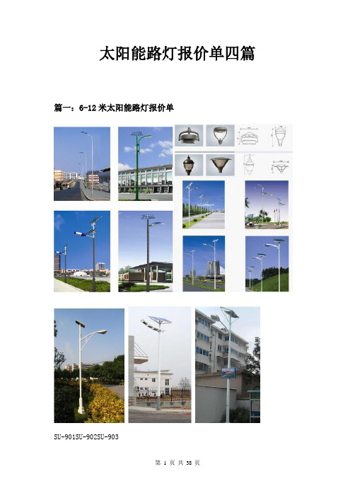
太阳能路灯报价单四篇篇一:6-12米太阳能路灯报价单SU-901SU-902SU-903SU-904SU-905SU-906SU-907SU-908SU-909第12 页共38 页第14 页共38 页第16 页共38 页第18 页共38 页第20 页共38 页篇二:太阳能路灯报价表XX公司太阳能路灯报价单根据现场情况及建设方要求,本工程共设置太阳能路灯 34 盏,具体参数及报价如下:1、基本参数:灯具生产单位:廊坊亿润道路照明有限公司灯杆型号: 83672.价格:每盏灯价格为 4700 元。
(此价格包括材料价格、安装价格及普通税票)XX科技有限公司20XX 年 10 月 13 日太阳能路灯报价单灯源: 20 瓦 LED 保修期 2 年胶体电池: 100AH 保修期 3 年太阳能板: 80 瓦保修期 10 年热镀锌灯杆: 6 米保修期 10 年控制器:全功率此配置为优化后配置,能保证冬天日光弱得情况下,路灯有足够的工作时间报价:包括安装及带普通税票,每盏灯价格为 5600 元。
根据现场情况共需设置 34 盏灯。
有限公司20XX 年 10 月 13 日篇三:太阳能路灯报价表(总高6 米,光源高 5.5 米,日照系数 4 小时,每天工作 6 小时,联续阴雨天数3-5 天)名称规格数量价格说明电池板80W 1 285元多晶,寿命25 年,质保 5 年,功率正公差。
蓄电池12V70AH1 410元阀控密封胶体蓄电池,太阳能专用,寿命4-6年,质保 3 年,富威原包,容量正公差。
控制器12V10A 1 100元多种功能,防过充、过放,光控开,时控关,寿命 5 年,质保 2 年,国内著名品牌。
电池箱80 型号 1 20元压制成型,全密封防水,有较好的保温作用,寿命20 年,质保 5 年。
2.5mm 14m 40 纯铜,十足线径电线及螺丝元 2.0MM ,护套双股线。
含灯具主光源30W 1 150元台湾芯片,质保 3 年,灯具可选(小金豆、新星、兰花等多种)灯杆加太阳能支架6 米 1 490元口径70-150 ,壁厚2.75 ,臂出1 米,A字臂或类似不太复杂的灯杆,含组件支架。


1200AP40 1200AP60、1203P60200D6、203D6 DAP8A 可互代203D6/1203P6 DAP8A2S0680 2S08803S0680 3S08805S0765 DP104、DP7048S0765C DP704加24V得稳压二极管ACT4060 ZA3020LV/MP1410/MP9141ACT4065 ZA3020/MP1580ACT4070 ZA3030/MP1583/MP1591MP1593/MP1430ACT6311 LT1937ACT6906 LTC3406/A T1366/MP2104AMC2576 LM2576AMC2596 LM2596AMC3100 LTC3406/AT1366/MP2104AMC34063A AMC34063AMC7660 AJC1564AP8012 VIPer12AAP8022 VIPer22ADAP02 可用SG5841 /SG6841代换DAP02ALSZ SG6841DAP02ALSZ SG6841DAP7A、DP8A 203D6、1203P6DH321、DL321 Q100、DM0265RDM0465R DM/CM0565RDM0465R/DM0565R 用cm0565r代换(取掉4脚得稳压二极管) DP104 5S0765DP704 5S0765DP706 5S0765DP804 DP904FAN7601 LAF0001LD7552 可用SG6841代(改4脚电阻)LD7575PS 203D6改1脚100K电阻为24KOB2268CP OB2269CPOB2268CP SG6841改4脚100K电阻为2047KOCP1451 TL1451/BA9741/SP9741/AP200OCP2150 LTC3406/AT1366/MP2104OCP2160 LTC3407OCP2576 LM2576OCP3601 MB3800OCP5001 TL5001OMC2596 LM2596/AP1501PT1301 RJ9266PT4101 AJC1648/MP3202PT4102 LT1937/AJC1896/AP1522/RJ9271/MP1540SG5841SZ SG6841DZ/SG6841DSM9621 RJ9621/AJC1642SP1937 LT1937/AJC1896/AP1522/RJ9271/MP1540STRG5643D STRG5653D、STRG8653DTEA1507 TEA1533TEA1530 TEA1532对应引脚功能接入THX202H TFC719THX203H TFC718STOP246Y TOP247YV A7910 MAX1674/75 L6920 AJC1610VIPer12A VIPer22A[audio01]ICE2A165(1A/650V、31W);ICE2A265(2A/650V、52W);ICE2B0565(0、5A/650V、23W):ICE2B165(1A/650V、31W);ICE2B265(2A/650V、52W);ICE2A180(1A/800V、29W);ICE2A280(2A/800、50W)、KA5H0365R, KA5M0365R, KA5L0365R, KA5M0365RN# u) t! u1 W1 B) R, PKA5L0365RN, KA5H0380R, KA5M0380R, KA5L0380R1、KA5Q1265RF/RT(大小两种体积)、KA5Q0765、FSCQ1265RT、KACQ1265RF、FSCQ0765RT、FSCQ1565Q这就是一类得,这些型号得引脚功能全都一样,只就是输出功率不一样。

905nm脉冲激光二极管驱动电路的设计905nm脉冲激光二极管在许多领域都有广泛的应用,如通信、激光雷达、光学传感等。
为了充分发挥其性能,一个优秀的驱动电路是必不可少的。
本文将详细介绍一种针对905nm脉冲激光二极管的驱动电路设计。
一、电路设计1. 电源供电驱动电路需要稳定的电源供电以提供所需的电压和电流。
我们选择一个开关电源,通过DC-DC转换器将输入电压转换为稳定的输出电压。
这种转换器具有高效率、低噪声和良好的负载响应特性。
2. 脉冲发生器为了产生脉冲激光,我们需要一个脉冲发生器。
我们选择一个基于TTL (Transistor-Transistor Logic)的脉冲发生器,它可以产生高速脉冲信号。
TTL脉冲发生器具有陡峭的前沿和后沿,能够确保激光二极管在脉冲期间正常工作。
3. 激光二极管驱动器激光二极管驱动器是核心部分,它需要能够提供足够的电流驱动激光二极管。
我们选择一个具有高带宽、低噪声和高驱动能力的驱动器。
该驱动器能够根据脉冲发生器的信号驱动激光二极管,使其在脉冲期间正常工作。
4. 反馈控制电路为了确保稳定的输出功率,我们设计了一个反馈控制电路。
该电路通过监测激光二极管的输出功率,调整驱动器的输出电流,从而保持输出功率稳定。
二、电路优化为了提高驱动电路的性能,我们采取了以下优化措施:1. 降低噪声:我们选择低噪声元件,并在电路中加入去耦电容,以降低电源噪声和电磁干扰。
2. 提高效率:我们优化电源电路的设计,降低功耗和热损耗,提高整个驱动电路的能效。
3. 保护二极管:我们设计了一个快速关断电路,能够在异常情况下快速关闭激光二极管,防止其损坏。
4. 温度补偿:我们加入了温度传感器和补偿电路,以补偿温度对激光二极管性能的影响。
三、总结本文介绍了一种针对905nm脉冲激光二极管的驱动电路设计。
该设计考虑了电源供电、脉冲发生器、二极管驱动器和反馈控制电路等多个方面,并进行了优化措施以提高性能。
这种驱动电路能够为905nm脉冲激光二极管提供稳定的、高效的驱动能力,使其在各种应用中发挥出色的性能。

三菱PLC主控指令的用法第一篇:三菱PLC主控指令的用法三菱FX系列 PLC主控指令FX系列PLC有基本逻辑指令20或27条、步进指令2条、功能指令100多条(不同系列有所不同)。
本节以FX2N为例,介绍其基本逻辑指令和步进指令及其应用。
FX2N的共有27条基本逻辑指令,其中包含了有些子系列PLC的20条基本逻辑指令。
主控指令(MC/MCR):(1)MC(主控指令)用于公共串联触点的连接。
执行MC后,左母线移到MC触点的后面。
(2)MCR(主控复位指令)它是MC指令的复位指令,即利用MCR指令恢复原左母线的位置。
在编程时常会出现这样的情况,多个线圈同时受一个或一组触点控制,如果在每个线圈的控制电路中都串入同样的触点,将占用很多存储单元,使用主控指令就可以解决这一问题。
MC、MCR指令的使用,利用MC N0 M100实现左母线右移,使Y0、Y1都在X0的控制之下,其中N0表示嵌套等级,在无嵌套结构中N0的使用次数无限制;利用MCR N0恢复到原左母线状态。
如果X0断开则会跳过MC、MCR 之间的指令向下执行。
MC、MCR指令的使用说明:(1)MC、MCR指令的目标元件为Y和M,但不能用特殊辅助继电器。
MC占3个程序步,MCR占2个程序步;(2)主控触点在梯形图中与一般触点垂直。
主控触点是与左母线相连的常开触点,是控制一组电路的总开关。
与主控触点相连的触点必须用LD或LDI指令。
(3)MC指令的输入触点断开时,在MC 和MCR之内的积算定时器、计数器、用复位/置位指令驱动的元件保持其之前的状态不变。
非积算定时器和计数器,用OUT指令驱动的元件将复位,当X0断开,Y0和Y1即变为OFF。
(4)在一个MC指令区内若再使用MC指令称为嵌套。
嵌套级数最多为8级,编号按N0→N1→N2→N3→N4→N5→N6→N7顺序增大,每级的返回用对应的MCR指令,从编号大的嵌套级开始复位。
第二篇:三菱PLC脉冲指令文档PLSY脉冲输出指令PLSY有两个源操作数[S1S2}和一个目标地址操作数[D].S1指定脉冲频率,S2指定脉冲数,D指定脉冲输出元件号(对于三菱小型PLC,如FX系列只能选晶体管输出型且只能是Y0Y1Y2).PLSR脉冲指令的加减速度时间有这样程序:I------I I--------[PLSR K150 K600 K3000 Y000] 当X10接通时,Y0输出15Hz脉冲,在加速的3秒时间里,Y0输出的脉冲频率分10级增加,加速到150Hz时,加速过程需要225个脉冲,加速到150HZ时,以150Hz恒定频率输出150个脉冲后,开始减速,减速也是分为10级减少,当减到为0时,也刚好输出600个脉冲。

几款平民级的国产功放几款平民级的国产功放在投资受到限制的情况下,选择国产放大器是一种聪明的做法,这样可以将资金更多地分配给音箱和音源其实,国产功率放大器经过多年的发展完善,已经不再是当初的“猪肉机”了。
最为明显的进步是外观,其造型设计已经脱离了以往的俗气,显得越来越有品味。
面板和机箱的加工工艺受到厂家的高度重视,与价格更高的进口机相比已经难分伯仲。
其次,国产功放广泛借鉴优秀的线路设计,用料也越来越精,音质表现与中档次的进口机相比已经没有多少差距。
在一些方面甚至还超过部分进口器材。
在众多的国产功放当中,两千元以内的合并机拥有最广泛的消费群。
我们在这个价位挑选出市场上口碑较好的九个品牌做了一次集中测评,以期望能对读者购买起一定的参考作用。
测评的结果分为两部分,前一部分为每台机器的客观性描述,包括外观、功能、工艺结构和用料等。
后一部分则是主观听音结果。
一、奥斯DC-80杭州中裕技术发展公司的奥斯DC-80是晶体管放大器中的新秀。
朴实无华但做工精湛的而板上只有最基本的输人选择和音量旋钮,转动时的手感非常舒适。
背面板的镀金RCA插座提供了AUX、TUNER、TAPE、CD四路输入。
喇叭端子也镀金,可以适应裸线头、香蕉插和接线叉三种驳接方式。
交流供电使用插座,能方便地更换更高级的电源线。
当然,很少有人为一台一干多元的合并式放大器换电源线,但DC-80毕竟提供了这种可能机器的用科也无可挑剔:1/2W金属膜电阻、ELNA电解电容、ALPS音量电位器……,就连电路板到喇叭端子的一小段连线都是专门的音箱线。
DC-80从头至尾都采用场效应管,输入级是由孪生场效位管2SK389以及2SJ109构成的互补差分电路。
推动级由日立公司的2SK214/2SJ77中功率MOS管担任,推挽输出级也采用日立的MOS管,型号为2SKl058/2SJ162,DC-80的电源部分由一只在发烧发中口碑甚佳的320W山西太原“声达”环变和两只l0000u"红宝石"电容组成,应付80W的额定输出显得绰绰有余。


电路分析(fēnxī)基础实验指导书电路(diànlù)分析基础实验指导书《电路(diànlù)分析基础》实验教学指导书前言一、实验(shíyàn)总体目标初步(chūbù)具备电压表、电流表、万用表等电工(diàngōng)实验设备的操作使用(shǐyòng)能力和电路仿真软件(ruǎn jiàn)的应用能力,根据实验任务确定实验方案、设计实验线路和选择仪器设备,正确测量参数和处理数据。
二、适用专业年级电子信息工程、通信工程专业一年级本科学生。
三、先修课程《高等数学》、《大学物理》。
电工综合实验台:40套。
主要配置:直流电路模块实验板、动态电路模块实验板、多路直流电压源、多路直流电流源、信号源、直流电压表、直流电流表、示波器等。
Multisim电路仿真分析软件。
六、实验(shíyàn)总体要求1、正确(zhèngquè)使用电压表、电流表、万用表、功率表以及一些电工实验设备;2、按电路图联接实验线路和合理布线,能初步(chūbù)分析并排除故障;3、认真观察实验(shíyàn)现象,正确读取实验数据和记录实验波形并加以检查和判断,正确书写实验报告和分析实验结果;4、正确运用实验(shíyàn)手段来验证一些定理和结论。
5、具有根据实验任务确定实验方案、设计实验线路和选择仪器设备的初步能力。
6、按每次实验的具体要求认真填写实验报告。
七、本课程实验的重点、难点及教学方法建议本课程实验的重点是仪表的正确使用、电路的正确连接、数据测试和分析;本课程实验的难点是动态电路参数测试和分析。
在教学方法上,本课程实验应提前预习,使学生能够利用原理指导实验,利用实验加深对电路原理的理解,掌握分析电路、测试电路的基本方法。
目录实验(shíyàn)一电阻电路测量与分析综合实验 (1)实验二电源(diànyuán)等效电路综合实验 (11)实验(shíyàn)三动态(dòngtài)电路仿真实验(shíyàn) (18)实验四RC频率特性和RLC谐振仿真实验 (24)实验一电阻电路(diànlù)测量与分析综合实验一、实验(shíyàn)目的1、熟悉并掌握(zhǎngwò)直流电压表、电流表、恒压源等使用;2、学会(xuéhuì)电阻元件的伏安特性的逐点测试法;3、学会(xuéhuì)电路中电位、电压的测量方法,掌握电路电位图的测量、绘制方法;4、验证基尔霍夫定律,学会检查、分析电路简单故障;5、验证叠加原理,学会叠加原理的应用。


90系列三极管参数90系列三极管大多是以90字为开头的,但也有以ST90、C或A90、S90、SS90、UTC90开头的,它们的特性及管脚排列都是一样的。
90系列三极管引脚图9011 结构:NPN集电极-发射极电压30V集电极-基电压50V射极-基极电压5V集电极电流0.03A耗散功率0.4W结温150℃特怔频率平均370MHZ放大倍数:D28-45 E39-60 F54-80 G72-108 H97-146 I132-1989012 结构:PNP集电极-发射极电压-30V集电极-基电压-40V射极-基极电压-5V集电极电流0.5A耗散功率0.625W结温150℃特怔频率最小150MHZ放大倍数:D64-91 E78-112 F96-135 G122-166 H144-220 I190-3009013 结构:NPN集电极-发射极电压25V集电极-基电压45V射极-基极电压5V集电极电流0.5A耗散功率0.625W结温150℃特怔频率最小150MHZ放大倍数:D64-91 E78-112 F96-135 G122-166 H144-220 I190-3009014 结构:NPN集电极-发射极电压45V集电极-基电压50V射极-基极电压5V集电极电流0.1A耗散功率0.4W结温150℃特怔频率最小150MHZ放大倍数:A60-150 B100-300 C200-600 D400-10009015 结构:PNP集电极-发射极电压-45V集电极-基电压-50V射极-基极电压-5V集电极电流0.1A耗散功率0.45W结温150℃特怔频率平均300MHZ放大倍数:A60-150 B100-300 C200-600 D400-10009016 结构:NPN集电极-发射极电压20V集电极-基电压30V射极-基极电压5V集电极电流0.025A耗散功率0.4W结温150℃特怔频率平均620MHZ放大倍数:D28-45 E39-60 F54-80 G72-108 H97-146 I132-1989018 结构:NPN集电极-发射极电压15V集电极-基电压30V射极-基极电压5V集电极电流0.05A耗散功率0.4W结温150℃特怔频率平均620MHZ放大倍数:D28-45 E39-60 F54-80 G72-108 H97-146 I132-198以上可以看出不同型号的90系列三极管放大倍数分档是不一样的,替换时要注意型号后面的后缀。

Catalog2013Electronic Timing RelaysType JCK Class 9050˚Application, General Information. . . . . . . . . . . . . . . . . . . . . . . . . . . . . . . . . . . . . . . 4˚Selection. . . . . . . . . . . . . . . . . . . . . . . . . . . . . . . . . . . . . . . . . . . . . . . . . . . . . . . . . 6˚Specifi cations . . . . . . . . . . . . . . . . . . . . . . . . . . . . . . . . . . . . . . . . . . . . . . . . . . . . . 8˚Dimensions, Wiring Diagrams. . . . . . . . . . . . . . . . . . . . . . . . . . . . . . . . . . . . . . . . . 9˚Accessories . . . . . . . . . . . . . . . . . . . . . . . . . . . . . . . . . . . . . . . . . . . . . . . . . . . . . 103General InformationTiming Functions9050JCK Electronic Timing Functions49050JCK Electronic Timing FunctionsA pplication,General Information (continued)Type JCK Electronic Timing Relays 5Variable Time DelaySpecify the voltage code when ordering this product. Refer to the standard voltage codes listed below and insert the code as shown in “How To Order” below.Fixed Time DelaySpecify the voltage code when ordering this product. Refer to the standard voltage codes listed below and insert the code as shown in “How To Order” below.(1) (XXXX) denotes desired timing period in seconds. Example: Class 9050 Type JCK1F60 is an On Delay timer fixed at 60 seconds.(2) F ixed repeat cycle timers are available with the same On and Off Times (for example., 9050JCK5F130V20) or different On and Off Times (for example,9050JCK5F130F35V20). Specify the suffix for the Off Time (F130), then the suffix for the On Time (F35).Voltage CodesFeatures:˚Up to ±0.1% repeat accuracy˚Timing from 0.1 seconds to 120 minutes ˚Available in 7 different timing functions ˚DPDT contacts (2 N.O. & 2 N.C.) ˚10 A contact rating˚Transient protected˚Hold-down spring available ˚Variable or fixed time delay ˚Horsepower rated9050JCK11V209050JCK1F15V149050JCK11V146Programmable TimersClass 9050 Type JCK programmable timers are microprocessor controlled to provide flexibility with accurate timing. The Type JCK60 On Delay timer has seven programmable timing ranges. The Type JCK70 multifunction timer has 10 timing functions and seven programmable timing ranges. T o program the timers, remove power and select the timing range and timing functions. Settings of less than 0.05 seconds are not recommended due to the response time of the electromechanical outputs.Type JCK60 (On Delay)This On Delay timer uses a push-button thumbwheel to select the timing range, and uses three push-button thumbwheels to select the time value.(1) The voltage code must be specified to order this product. Refer to standard voltage codes listed below and insert the code as shown in “How To Order” below.Type JCK70 (Multifunction)One 10-position push button thumbwheel is used to select the function. Three 10-position push button thumbwheels are used to select the timevalue. One 7-position push button thumbwheel is used to select the timing range.(1) The Repeat Cycle function uses the same On and Off times.(2) Specify the voltage code when ordering this product. Refer to the standard voltage codes listed below and insert as shown in How To Order.Note: Turn off power to the 9050JCK70 before changing the timing function.Voltage CodesFeatures:˚Up to ±0.1% repeat accuracy˚Timing from 0.05 seconds to 999 hours ˚Available in up to 10 timing functions ˚DPDT contacts (2 N.O. & 2 N.C.) ˚10 A contact rating˚Transient protected˚Hold-down spring available ˚Wide timing range ˚Horsepower ratedHow to Order Type JCK Timers7Operating Specifications(1) T he product life expressed on this page is based on average and normal operating conditions. Actual life will vary with conditions. The above statements are notintended to, nor shall they, create any expressed or implied warranties as to product operation or life. For more information on the listed warranty offered on this product, refer to the Terms and Conditions of sale found in the Digest.Electromagnetic Compatibility (EMC) Ratings (1) S upply port, output port, and control port LED Indicators(1) (1) T he LED is not an indicator of theoutput state of the timing relay.8Wiring DiagramsAC Maximum Contact RatingsNOTES:• U se the same voltage for the power trigger and control power. Do not use terminal 6 with power trigger devices.• F or timers that use trigger switches, the maximum distance for the triggerswitch is 50 ft. from the timer.Dimensions of Type JCK60 and JCK70versions only.Wiring DiagramsDimensions — inches mmContact Derating CurveDC Maximum Contact RatingsAC15/B300 (NO/NC), DC13/R300 (NO)Recommended minimum load current is 100 mA @ 12 Vdc.Power T rigger+–L1L24811132965710+–C us tomer su pplied s witch for power triggerL1L2Type (1):JCK11 – JCK19JCK31 – JCK39JCK51 – JCK59JCK60Type (1):JCK21PT – JCK29PT JCK41PT – JCK49PTType (1):JCK70Control Power Control Power Control PowerType (1) (2):JCK21 – JCK29JCK41 – JCK49(1) Do not apply DC voltage to the 240 Vac timers (voltage code V24).(2) There is no internal jumper between pins 6 and 7.9Snapmount Sockets-Screw Terminal(1) T he 8501NR62 socket is approximately the same width as the base of the JCK timer. Use the wider NR61 where space permitsfor ease of wiring.Input CompatabilityThe Type JCK timer is not compatible with 2-wire AC input sensors. A hard contactrelay (for instance, a general purpose relay) must be interposed. Class 8501 Type NR sockets are designed for use with plug-in Class 9050 Type JCK timers. All sockets have pressure clamps that accept one or two #12–22 AWG wires. The recommended tightening torque for all terminals is 7–8 lb-in. ˚35 mm DIN 3 track mounting or direct panel mounting˚Tubular sockets available in easy-to-wire single tier or space-saving multi-tier versions ˚All sockets are stockedAccessoriesClass 8501 Hold-Down Spring8501NR628501NR528501NR618501NR518501NH710Wiring DiagramsAccessoriesSocket Dimensions and Wiring Diagrams — inches mmTerminal LocationTop View NR618501NR618501NR51LocationTerminal NR51View TopM 351468372875431169210TerminalLocationTerminal 8501NR528501NR62M 3NR52View Top NR62View Top Dimensions:Inchesmm11© 2013 Schneider Electric. All Rights Reserved Schneider Electric and Square D are trademarks owned by Schneider Electric Industries SAS or its af fi liated companies. All other trademarks are the property of their respective owners.9050CT9601R06/13 Replaces 9050CT9601R03/09 dated 11/2011/6/2013Schneider Electric USA, Inc.1415 S. Roselle RoadPalatine, IL 60067 USATel: 888-778-2733。
TO: List CPECR#: 500000000818 GE FanucPRODUCTUPDATENOTICE September 22, 2000 Logicmaster 90-30/20/Micro Software Package Version 9.05Programmer and ConfiguratorTCP/IP Windows 95/98 / Windows NT MS-DOS Box VersionIC641SWP316G - 3.5 inch 2HDSection 1OverviewGeneral Description Logicmaster 90-30/20/Micro TCP/IP Windows NT/95/98 DOS Box product Release9.05 allows communication to the Series 90-30 PLC via a Series 90-30 Ethernet moduleor the PLC serial ports. It operates in an MS-DOS Box within Windows NT orWindows 95/98 (not under Windows 3.x).Beginning with Release 5.01, Sequential Function Chart programming capability isavailable by ordering the desired Logicmaster 90-30 version and the SFC ProgrammerOption diskette (IC641SWP311). Refer to the inside Section 3, New FeaturesIntroduced in Release 9.05 for details of new features introduced by this release.Problems fixed by this release are listed in Section 7, Problems Resolved by Release9.05. There are a couple of minor changes in the way Logicmaster 90-30/20/MicroRelease 9.04 interfaces with Series 90-20 PLCs; refer to Section 4, Changes AffectingSeries 90-20 PLCs, for details.H/W Identification: Not ApplicableS/W Identification: Ver. 9.05 LabelReplaces Version 9.02 and earlier versions2GE Fanuc PRODUCT UPDATE NOTICECompatibility Release 9.05 of Logicmaster TCP/IP Ethernet software requires a version 8.3 or later Series 90-30 CPU and 90-30 Ethernet Interface module(s) with Version 1.10 or latersoftware.If you are using the Standard Serial port version at the same time as theEthernet version, the Standard Serial port version should be version 6.5 or later for bestinter-operability.CAUTIONFolders created with all earlier releases of LM90-30 software are upwardly compatible.Folders created with LM90-30 version 9.05 are fully compatible with LM90-30 3.50 orlater. However, once a logic program or configuration is created or modified withRelease 9.05 of Logicmaster 90-30 it can not be used with LM90-30 Release 3.02 orearlier software. Also once a logic program or configuration is stored to a PLCwith Release 9.05, the program MUST NOT be loaded by an LM90-30 releaseearlier than 3.50. If you attempt to use a folder created in Release 9.05 with Release3.02 or earlier software, you will receive one of two messag es “Folder contains fileswhich are incompatible with this release” or “Program file corrupted”.Update Strategy An update to LM90-30 Release 9.02 or later is required for use with Series 90-30 CPU364. Logicmaster 90-30 customers with active subscriptions will automaticallyreceive the update.Documents IPI:GFK-1412GRef. Manual:GFK-0467KUser Manual:GFK-0466L, GFK-1401SFC User Manual: GFK-0854AGE Fanuc PRODUCT UPDATE NOTICE3Section 2Special Operational NotesSYSTEM REQUIREMENTS1.Windows NT version 4.0 or later, or Windows 95/98. For Windows NT 4, Service Pack 3 is recommended.Service Packs can be obtained from Microsoft.2.The Windows Networking and Microsoft TCP/IP protocol software distributed with Windows must be installed.3.Processor:∙ Windows 95/98: 486 33mhz or higher∙ Windows NT: 486 66mhz or higher4.8 Mb of available hard disk space.5.Available Memory:∙ Windows 95/98: 16 MB∙ Windows NT: 24 MB6.This release of Logicmaster 90-30/20/Micro requires at least 545 KB of free Conventional memory. If you see amemory size warning message when you attempt to start LM90, use the MS-DOS MEM /C command to discover the device drivers and TSR programs loaded in conventional memory. You will need to remove some of them from the CONFIG.SYS and/or AUTOEXEC.BAT files in your computer in order to provide the required conventional memory. If you are communicating with the PLC serially, you can also obtain additional conventional memory by configuring LM90 to load the serial communications driver into EMS memory. This is accomplished by the following steps:1) From Menu90 select F9 .... Logicmaster 90 Setup Package2) Then select F4 ... PLC Communication Options3) Select EMS for the "Driver Memory Area".7.Operation of Logicmaster 90 via serial communication, including dial-up networking, requires a serial controllerdevice that supports a first-in-first-out (FIFO) character buffer. If the serial controller device has no FIFO, intermittent program lockups which require rebooting the PC may occur. To determine which serial controller device your PC uses, open Control Panel and select Modems. Follow the procedure to “install” a modem, clicking next at every choice and selecting the serial Comm. port through which Logicmaster will communicate.No modem need be physically present to p erform this “installation”. After completing the “installation”, select Diagnostics and wait for the More Info screen to appear (if an error message appears, click OK). The More Info screen will display the serial controller device type present. If the type is NS16550, a FIFO buffer is supported.For other types, consult appropriate technical specifications and/or change serial interfaces. It is also recommended that the “FIFO Enabled” option in the advanced settings for the serial port is enabled. Th is setting is found by selecting the “Ports” icon with Control Panel.LOGICMASTER 90 INSTALLATIONFor detailed instructions on installing the Logicmaster 90 TCP/IP Windows software, refer to Chapter 3 of the Logicmaster 90 TCP/IP Windows 95/Windows NT, Use r’s Manual Supplement,GFK-1401. Remember that Logicmaster 90 software is licensed to run on a single computer. Since this is the initial installation you must enter the serial number found on the back of your disks.NoteOnce the LM90-30 TCP/IP version is installed on a disk, you should not attempt to install theSerial Port version of LM90-30. Since the Ethernet and Serial Port versions share the samedirectories this would result in loss of the Ethernet functionality. The TCP/IP version includes afully functional Serial Port version.4GE Fanuc PRODUCT UPDATE NOTICESFC PROGRAMMER INSTALLATIONThe Sequential Functional Chart (SFC) Programmer (IC641SWP311) diskette updates Logicmaster 90-30/20/Micro Release 5 or later to provide SFC programming capability. For Logicmaster 90-30 TCP/IP Windows software, inserting the IC641SWP3111 diskette during Logicmaster 90 installation enables SFC programming. To enable SFC programming after Logicmaster 90-30 TCP/IP for Windows is installed, you must perform the installation again. DEMO VERSION (IC641SWP703)The Logicmaster 90-30/20/Micro Demo version will install into the LM90DEMO directory on the hard disk specified during the install. For example, if you specify that the demo version software be installed on the C: drive, it will be installed in the C:\LM90DEMO directory. To run the demo software type the following from the DOS prompt:C:> CD LM90DEMOC:> LM90DEMOThe demonstration software is identical to the released version. However, program size is limited to 750 bytes for_MAIN, 750 bytes/program block, and Ethernet communication is unavailable.LOAD/STORE MAY DISRUPT OTHER COMMUNICATION LINKSWhen loading from or storing to the PLC using the LM90-30 TCP/IP version, PLC scan time may be lengthened due to the many messages sent to the PLC from the Ethernet Interface. Additionally, other TCP/IP traffic (such as Channels or data transfer to a host computer) processed by the Interface that is performing the load/store may experience delays and even timeouts.When loading from or storing to the PLC using the LM90-30 TCP/IP version, other communication modules (PCMs, CMMs, GBCs, and Ethernet) may experience delays while communicating to the CPU. In extreme cases where the load or store is very large, a communication error may be returned. In these cases, a retry of the communications should correct the error.LONG DISCONNECTIONS FROM PLC MAY REQUIRE RE-STARTING LM90Beginning with Release 7.05, if Logicmaster is physically disconnected from the PLC for periods of 1/2 hour or greater, the user may be required to close and re-start Logicmaster in order to re-gain communications with the PLC. In previous versions of Logicmaster, this time limit did not exist.DETERMINING IF AN IP ADDRESS HAS ALREADY BEEN USEDTo determine if you have configured your station (Logicmaster 90-30 TCP/IP for Windows) with the same IP address as another station, disconnect the station in question from the LAN, then try a PING command to that IP address from another station. If you get an answer to your PING, then the chosen IP address is already in use. (Refer to the next section TESTING TCP/IP SOFTWARE AFTER INSTALLATION for instructions on using the Ping command).LOGICMASTER OPERATION MAY RESULT IN PLC FAULTNormal use of Logicmaster Windows with Ethernet or Dial-up net communications may result in the occurrence of PLC fault table entries of the type “Connection to remote node failed; resuming w/o it”. The corresponding entries will appear in the Series 90 Ethernet Interface exception log (type=12, entry 2 = F) and its STAT LED will be off. These entries should be ignored. The condition that they indicate is not serious and does not occur with Ethernet Interfaces IC693CPU364 Version 1.0 and IC693CMM321 version 2.10 and later.GE Fanuc PRODUCT UPDATE NOTICE5RUN-MODE PROGRAM STORE ALLOWED WITH LEVEL 3 PASSWORD ACCESSWhen Logicmaster 90-30 is used with a PLC containing CPU firmware version 6.61 or later, changes to the PLC program while the PLC is in RUN mode are erroneously allowed at PLC password access level 3. This error can occur when you edit the program in OFFLINE mode, switch to ONLINE mode using the Alt-M key combination, and then press the Esc key. Logicmaster will update the folder and prompt to update the PLC. Typing "y" at this point causes a RUN-mode program store to the PLC that should require access level 4.DO NOT ATTEMPT TO START MORE THAN ONE LOGICMASTER 90 WINDOWSeveral problems can occur when you attempt to start two or more Logicmaster 90 windows at the same time:∙Logicmaster 90 does not support access to the same folder by two or more processes at the same time. Under Windows 95/98, Logicmaster 90 will complain about file sharing violations or that the disk drive is read-only. ∙Logicmaster 90 will not permit more than one Programming Software package and one Configuration Software package for the same CPU type to run at the same time from the same \LM90 directory.∙Under Windows 95/98, real time data updates on the Logicmaster 90 Program Display/Edit or Reference Tables page may stop when two or more Logicmaster 90 windows use TCP/IP to connect to PLCs at the same time. APPLICATION ERRORS CAN OCCUR UNDER WINDOWS NT 3.51Under Windows NT version 3.51 only, Windows displays “Access Violation” or “Application Error” messages in certain circumstances. When you exit from the Logicmaster 90 Programmer or Configuration Software while an unsuccessful PLC connection is pending, and the Logicmaster 90 TCP window remains open about 45 seconds longer, one of these errors will occur. This problem happens when you assign an incorrect IP address, or the target PLC is powered off or unreachable. To recover, click OK in the error message box, exit from the Logicmaster 90 Main Menu, close the Logicmaster 90 TCP window, and start Logicmaster 90 again.NETWORK UTILITIES AND LOGICMASTER 90 USE DIFFERENT NETWORK ADDRESS FILES WHEN LOGICMASTER 90 IS INSTALLED ON TWO OR MORE DISK DRIVESWhen any version of Logicmaster 90 is already installed on drive C at the time Logicmaster 90 Windows is installed on another drive, the Network Utilities program in Logicmaster 90 Windows will access PLC network address files on drive C, while the Logicmaster 90 Windows Programming and Configuration software will access PLC network address files on the drive where they were installed. This may prevent you from assigning and using PLC network addresses. You can correct this problem.∙For Windows NT version 4.0 or Windows 95/98, use Start/Programs/Windows Explorer to view the contents of the LM90 directory on the new drive. Select the icon for LM90_NTw, LM90_NTf, LM90_95w, or LM90_95f (depending on the Windows version and the setup options you chose), press the right mouse button, and select Properties. In the Properties dialog box, select the Program tab, place the mouse cursor in the Cmd line box after “LM90.BAT”, and change the “C” drive letter in “C:\LM90” to the correct drive letter. Then click OK.∙For Windows NT version 3.51, click the Logicmaster TCP icon in the PLC Programmer program group. On the Program Manager File menu, select Properties. Note the file path and name of the PIF file in the Command Line window. Click the Cancel button. Double click PIF Editor in the Main program group, click Open in the File menu, and use the Drives and Directories windows to find the path and file name of the PIF file you previously identified. Select the PIF file in the File name window and click OK. In the Optional Parameters window, change the “C” drive letter in “C:\LM90” to the correct drive letter. Then click OK.DO NOT CHANGE THE FILE PATH FOR NETWORK ADDRESS FILES ON THE LOGICMASTER 90 SELECT PLC CONNECTIONS SCREENIf you have more than one Logicmaster 90 directory, and you change the file path for the network address files on the Logicmaster 90 Programmer Mode and Setup/Select PLC Connections(F7/F3) screen, the Windows TCP/IP6GE Fanuc PRODUCT UPDATE NOTICEcommunication driver will be unable to find the IP address for the most recent PLC connection the next time Logicmaster 90 is started. This will prevent Logicmaster 90 from establishing a connection.WINDOWS MESSAGE WARNS THAT TCP/IP COMMUNICATION DRIVERS ARE NOT INSTALLED If TCP/IP communication software has not been installed on your computer, you will see one of these Windows warning messages:You must install networking software and the TCP/IP network protocol before using this software.The TCP/IP network protocol must be installed before using this software. See the 'Installing TCP/IP and SNMP' and 'Configuring TCP/IP' topics in Control Panel Help.The text for these messages is English only.CTRL-BREAK DOES NOT WORK IN WINDOWS NT VERSION 3.51 WITHOUT SERVICE PACK 5 Under Windows NT version 3.51, the Ctrl-Break key combination does not cause Logicmaster 90 to display the expected "Exit Logicmaster 90 Programmer/Configuration Package? (Y/N)" prompt. This restriction is corrected by Service Pack 5 (available from Microsoft), and does not apply to Windows NT version 4.0 or Windows 95/98. TESTING TCP/IP SOFTWARE AFTER INSTALLATIONAfter installing the software, you should verify that communications can be established. To test the TCP/IP software after installation, do the following:First, PING from the PC to the PLC with the following procedure:1.Determine the IP address of the PLC Ethernet module. Assume for the purposes of this example that the IPaddress is 10.16.32.64.2.From the DOS prompt, enter the following command (use actual IP address):C:\> PING 10.16.32.643.The command line display will look something like the following:PING 10.16.32.64 : xx data bytesxx bytes from 10.16.32.64 : icmp_seq=0. time=xxx. msxx bytes from 10.16.32.64 : icmp_seq=1. time=xxx. msxx bytes from 10.16.32.64 : icmp_seq=2. time=xxx. ms4.After five or more lines have been displayed, enter Control-C to stop the PING utility. This will display thePING statistics, which will look similar to the following:__________ 10.16.32.63 PING Statistics _______xx packets transmitted, xx packets received, xx% packet lossround-trip (ms) min/avg/max xx/xx/xx5. A correctly functioning PING command will show a zero percent (0%) packet loss.If the PC-to-PLC PING (described above) works successfully, then PING from the PLC to the PC with the following procedure:1.Determine the IP address of the PC running the TCP/IP driver. Assume for the purposes of this example that theIP address is 10.16.32.65.2.To issue the Ping command from the PLC Ethernet module, you must have access to the Ethernet module’sStation Manager which you can do by connecting a terminal emulator or dumb terminal to RS-232 port of the PLC Ethernet module using the included cable IC693CBL316. For details about the Station Manager, refer to GFK-1186, also included.GE Fanuc PRODUCT UPDATE NOTICE7 From the terminal, enter the following station manager commands:1.Enter the Station Manager login command. This will prompt you for a password. The default password issystem. Once logged in, you will be at the Modify level.2.Enter the Station Manager command “ping 10.16.32.65” (except use the actual PC IP address). This willproduce PING statistics that look similar to the following:<<< Ping Results >>>Command: ping 10.16.32.65 1 100 64Remote IP Address: 10.16.32.65, Sent =1, Received=1, No Response=0Round-trip (ms) min/avg/max xx/xx/xx1. A correctly functioning PING command will show the number of Sent and Received packets equal and the “NoResponse” field equal to zero.USING MS-DOS TO COPY FOLDER FILESWarning: MS-DOS should not be used to copy individual files from one folder to another or to delete files; doing so may result in corrupted folders. MS-DOS may only be safely used to copy an entire program folder to another program folder of the same name. For most copying needs, however, use the Copy function within the Logicmaster 90-30 software.SERIAL PRINTINGThe serial ports, COM1 and COM2, can be used for serial printers. Beginning with Release 4.50, the serial printer port must be configured with the MS-DOS mode command to match the printer settings. Refer to Logicmaster 90-30 Programming Software User’s Manual, GFK-0466, chapter 6, section 6, Serial Print Setup for details.PLC COMMUNICATION OPTIONSThis product installs the Standard Serial Port, Ethernet and Dial-Up Networking communications options for Logicmaster 90. By default the Serial Port option is run. To use Ethernet or Dial-Up Networking communications, you must select one of these options. Refer to Chapter 3 of the Logicmaster 90 TCP/IP Windows 95/Windows NT, User’s Manual Supplement, GFK-1401.LOGICMASTER OPERATING VIA CMM MODULE AND OR 35X CPU SERIAL PORTS CAN REMAIN ONLINEWhen multiple instances of Logicmaster are connected to one PLC, there is typically only one instance of an Online programmer (an Online programmer can change the RUN/STOP state of the PLC). An exception to this operation can occur when Logicmaster instances are connected via a CMM module and or 35X CPU Serial port- these instances will remain in Online operation regardless of what other Online instances of Logicmaster are also connected.LOGICMASTER 30/20/MICRO SERIAL UNDER WINDOWSBeginning with Release 4.50 the Logicmaster 90-30/20/Micro Standard Serial COM Port Version can run under Windows, LM90-30/20/Micro may be run in windowed or full screen mode. (Previous versions may have worked in offline mode, but could not be used to communicate with the PLC.) To use Logicmaster under Windows, please observe the following guidelines:I.At least 42K in Expanded Memory (EMS), an Upper Memory Block (UMB), or the High Memory Area (HMA) mustbe available for the serial communications driver. If EMS memory is used for LM90-30/20/Micro, you must ensure that no other device driver or TSR is also using EMS memory.8GE Fanuc PRODUCT UPDATE NOTICEII.If you are running under Windows NT 3.51, you should install Service Pack 2 or later. If you are running under Windows NT 4.0, you should install Service Pack 3 or later. The following new Windows registry entries (values not keys) should be added (unless they are already present) using Windows REGEDT32 underHKEY_LOCAL_MACHINE\SYSTEM\CurrentControlSet\Control\WOW:(1) COM_SyncWrite : REG_SZ 1(2) COM_TxBuffer_Size : REG_SZ 1Setting these values will require that you have ADMINISTRATOR privileges for your computer.III.LM90-30/20/Micro Release 4.50 or later may be setup to use COM1, COM2, COM3, or COM4 as the communications port for communicating with the Series 90-30/20/Micro PLCs.IV. You should not attempt to run more than one session of LM90-30/20/Micro at the same time. Doing so may result in corruption of the program folders.V. However, you may bring up the Programming and Configuration software at the same time as long one of them is off-line or they both use different COM ports. Exercise care not to change the CPU model configured from the Configurator while you are in the program editor or reference tables in the programming software. If you wish to access the same folder from both the Programming and Configuration software packages, you will need to ensure that SHARE.EXE is not used in the AUTOEXEC.BAT file, or you will receive the message ”File System Error” .VI. For some display adapters and drivers, you may find that LM90 is not displayed in color in Windowed mode. However, LM90 will be displayed in color in Full Screen mode. You may switch between Windowed and Full Screen mode using the ALT-ENTER key.HAYES MODEMSWhen using Logicmaster 90 over a dial-up link using Hayes modems, problems can occur if the connection between the local modem and the PC disconnected. When the cable is disconnected, the modem does not relinquish the telephone line. You must cycle power on the modem or disconnect the telephone line in order to hang up the telephone connection. If the connection between the PC and the modem is removed and then reconnected, random characters may be sent from the modem to the PC causing Logicmaster to lose communications with the PLC. When using Hayes modems, care should be taken not to disconnect any cables to or between the modems.MODEM TURNAROUND TIMEThe Modem Turnaround Time (also known as TurnA Delay and Modem TT ) has a usable range of 0...148 (1.48 seconds) instead of the configurable range of 0..255. Using a turnaround time greater than 148 could cause a loss of communications that requires initializing the port to default values which include a 0 value for Modem Turnaround Time. Modem Turnaround Time is the serial port time required for the modem to start data transmissionafter receiving the transmit request.GE Fanuc PRODUCT UPDATE NOTICE9Section 3New Features Introduced in Release 9.051.Fatal Faults Ignore –Starting with release 9.05, the Low-end (311 thru 341) CPUs have a CPU configurationparameter which will, when enabled, ignore fatal faults.munications Drivers - This version ( release 9.05) of Logicmaster 90-30/20/Micro uses standard Windows32-bit drivers for communication ports and modems. These drivers improve communication reliability and support a wider range of modems. See “INSTALLATION ON SYSTEMS WITH LOGICMASTER 90-30/20/Micro”in section 2, Special Operational Notes, for information on installation issues. See “USING MODEMS” in section 2 for information on using modems with this version and “MS-DOS MODE IS NOT SUPPORTED” for information on a new restriction in this version.Section 4Changes Affecting Series 90-20 PLCsStarting with release 9.02, there are some minor changes to Logicmaster 90/30/20/Micro that affect the 90-20 PLC CPUs only.1.Configuration of Series 90-20 CPUs - To configure a 90-20 module, select 90-20(Shift-F2) from MENU90on the first Logicmaster screen before selecting Config (F2). You can no longer select 90-20 modules after you have entered the configuration software with 90-30 selected.2.Changing a 90-20 Configuration to a 90-30 Configuration - To change a 90-20 configuration to a 90-30configuration, you should perform the following steps:(a)Select 90-30 (Shift-F3) from MENU90 before selecting the Logicmaster 90 Configuration package.(b)When you enter I/O Configuration, you will notice that an “Unknown Module Placeholder” is shownfor the Series 90-20 CPU.(c)Determine the 11-digit catalog number for the 90-30 CPU that you want to configure.(d)Type the 11-digit catalog number into the Catalog # field and press Enter to replace the string“UNKNOWN-MOD”. Respond “Y” (yes) when asked if you wish to replace the CPU module.10GE Fanuc PRODUCT UPDATE NOTICESection 5Using LM90 Release 9.05 with Earlier CPU ModelsLogicmaster 90-30 Release 9.05 was designed and tested to be compatible with Release 9 or earlier Series 90-30, or Release 2 or earlier Series 90 Micro CPUs while still providing new Logicmaster features. However, some new features found in Release 9.05 Logicmaster 90-30 require an upgrade of CPU firmware to be fully available.SFC PROGRAMMINGPrograms that use SFC (Sequential Function Chart) Programming require CPU release 5.0 or later. SFC is not supported by the Series 90-20 or Series 90 Micro PLCs.SUBROUTINESSubroutines require a 90-30 CPU. They are not supported by the Series 90-20 or Series 90 Micro PLC.PERIODIC SUBROUTINESPeriodic Subroutines require a Release 4.20 or later 340 or 341 CPU. If a program contains a periodic subroutine it cannot be stored to a Series 90-30 CPU earlier than Release 4.20.NoteOnly Models 340 or higher (release 4.2 or later) PLCs support the use of a periodic subroutine atthis time. Only periodic subroutine names of the form 1Tnn are supported at this time (nn is anumber from 1 to 10 that specifies the number of milliseconds between executions of thesubroutine). Only one such subroutine is allowed.NEW INSTRUCTIONSThe Sequential Event Recorder (SER) instruction requires a CPU350 or higher with Release 9 or later firmware. The following floating-point instructions require a Release 9 or later Series 90-30 350 or higher CPU or a Release 7 or later 352 CPU.ADD_REAL, SUB_REAL, MUL_REAL, DIV_REAL, SQRT, SIN, COS, TAN, ASIN, ACOS, ATAN, LOG, LN, EXP, EXPT, EQ_REAL, NE_REAL, GT_REAL, GE_REAL, LT_REAL, LE_REAL, TO_REAL_BCD4, TO_REAL_INT, TO_REAL_WORD, TO_REAL_DINT, TO_INT_REAL, TO_DINT_REAL, TO_WORD_REAL, TRINT, TRDINT, MOVE_REAL, and BLKMV_REAL.Use of the above instructions with a CPU that does not support the instruction will result in one of the following messages when attempting to store to program to the PLC: “Store aborted; Program in folder uses inst ructions not supported by PLC” or “Program size too large for PLC or invalid user program.”GE Fanuc PRODUCT UPDATE NOTICE11Section 6Problems Resolved by Release 9.05Subject I DCodeDescriptionRelease of Serial Port 63093 After exit from LM90 the serial port that was used for serialcommunication was not released so that it could be used by otherapplications such as Control 90. This problem has been corrected. Read from Flash 67797 The upper limit for display of the LM90 Reference Tables was notcorrect after a read from Flash memory. This problem has beencorrected.LOGICMASTER LOSES COMMUNICATION DURING SERIAL STORE When storing logic, configuration, or reference tables using Serial communications, the operation may occasionally fail, producing a "Communications failed" error message. In some cases, the Logicmaster 90 TCP window may appear to be locked up until the PLC is powered off or the serial cable is disconnected. The PLC will post a “Program block checksum” or “PLC sequence store failure” fault in the PLC fault table and enter STOP/FAULT mode. This error does not occur using Ethernet or Dial-up net communications.Busy Please Wait .. or ID: 0000 EX: 0000 65507If you attempt to enter HW Configuration and the “Busy, please wait…” message occurs and the system locks up, or ID: 0000 EX:0000 occurs while configuring modules, you probably do not haveenough DOS conventional memory available.If you arecommunicating with the PLC serially, you can obtain additionalconventional memory by configuring LM90 to load the serialcommunications driver into EMS memory. This can be accomplishedby the following steps:1) From Menu90 select F9 .... Logicmaster 90 Setup Package2) Then select F4 ... PLC Communication Options3) Select EMS for the "Driver Memory Area".Load of CPU364 configuration 67854An attempt to load the configuration from a CPU364 after the ClearPLC configuration function has been performed will result in aLogicmaster 90 system error. You should store a configuration fromLM90 before attempting a load.。