RT-090505中文资料
- 格式:pdf
- 大小:84.88 KB
- 文档页数:2

DS9505-02 April 2011Featuresz 18V Maximum Rating for AC Adapter z Internal Integrate P-MOSFETsz AC Adapter Power Good Status Indicator z Charge Status Indicator z Under Voltage Protection z Over Voltage Protectionz Automatic Recharge Feature z Battery Temperature Monitoring z Small 10-Lead WDFN Packagez Thermal Feedback Optimizing Charge Rate zRoHS Compliant and 100% Lead (Pb)-FreePin ConfigurationsApplicationsz Digital Cameras z Cellular Phonesz Personal Data Assistants (PDAs)z MP3 Players zHand Held PCsOrdering InformationGeneral DescriptionThe RT9505 is a fully integrated low cost single-cell Li-Ion battery charger IC ideal for portable applications. The RT9505 is capable of being powered up from AC adapter.The RT9505 enters sleep mode when AC adapter is removed.The RT9505 optimizes the charging task by using a control algorithm including preconditioning mode, fast charge mode and constant voltage mode. The charging task is terminated as the charge current drops below the preset threshold. The AC adapter charge current can be programmed up to 1A with an external resister. The internal thermal feedback circuitry regulates the die temperature to optimize the charge rate for all ambient temperatures.The RT9505 features 18V maximum rating voltages for AC adapter. The other features are under voltage protection, over voltage protection for AC adapter supply and battery temperature monitoring.(TOP VIEW)WDFN-10L 3x3Note :Richtek products are :` RoHS compliant and compatible with the current require-ments of IPC/JEDEC J-STD-020.` Suitable for use in SnPb or Pb-free soldering processes.Marking InformationFor marking information, contact our sales representative directly or through a Richtek distributor located in your area.Linear Single Cell Li-Ion Battery Charger ICP : Pb FreeG : Green (Halogen Free and Pb Free)Typical Application CircuitDS9505-02 April 2011Function Block DiagramDS9505-02 April 2011Absolute Maximum Ratings (Note 1)zACIN Input Voltage --------------------------------------------------------------------------------------------------------−0.3V to 18V z EN Input Voltage -----------------------------------------------------------------------------------------------------------−0.3V to 6V z Output Current -------------------------------------------------------------------------------------------------------------1.2A z Power Dissipation, P D @ T A = 25°CWDFN-10L 3x3-------------------------------------------------------------------------------------------------------------0.926W z Package Thermal Resistance (Note 2)WDFN-10L 3x3, θJA -------------------------------------------------------------------------------------------------------108°C/W WDFN-10L 3x3, θJC -------------------------------------------------------------------------------------------------------8.2°C/W z Lead Temperature (Soldering, 10 sec.)-------------------------------------------------------------------------------260°C z Junction Temperature ----------------------------------------------------------------------------------------------------150°Cz Storage T emperature Range --------------------------------------------------------------------------------------------−65°C to 150°C z ESD Susceptibility (Note 3)HBM (Human Body Mode)----------------------------------------------------------------------------------------------2kV MM (Machine Mode)------------------------------------------------------------------------------------------------------200VElectrical Characteristics(ACIN = 5V, T A = 27°C, Unless Otherwise specification)To be continuedRecommended Operating Conditions (Note 4)z ACIN Input Voltage Range -----------------------------------------------------------------------------------------------4.5V to 6Vz Junction T emperature Range --------------------------------------------------------------------------------------------−40°C to 125°C zAmbient T emperature Range --------------------------------------------------------------------------------------------−40°C to 85°CNote 1. Stresses listed as the above“Absolute Maximum Ratings”may cause permanent damage to the device. These are for stress ratings. Functional operation of the device at these or any other conditions beyond those indicated in the operational sections of the specifications is not implied. Exposure to absolute maximum rating conditions for extended periods may remain possibility to affect device reliability.Note 2. θJA is measured in the natural convection at T A = 25°C on a high effective thermal conductivity test board (4 layers, 1S) of JEDEC 51-7 thermal measurement standard. The case point of θJC is on the expose pad for the package.Note 3. Devices are ESD sensitive. Handling precaution is recommended.Note 4. The device is not guaranteed to function outside its operating conditions.DS9505-02 April 2011Typical Operating CharacteristicsV BATT = 3.7VACIN Power OnTime (250us/Div)I CHARGE (0.5A/Div)V ACIN (5V/Div)V BATT = 3.7VACIN Power OffTime (500us/Div)I CHARGE (0.5A/Div)V ACIN (5V/Div)Input Voltage TransitionTime (500us/Div)I CHARGE (1A/Div)V ACIN (5V/Div)ACIN Power OnV BATT = 3.7VACIN Power OffInput Voltage TransitionTime (500us/Div)I CHARGE (1A/Div)V ACIN (5V/Div)V BATT = 3.7VACIN = 0V to 10V, V BATT = 3.7VACIN OVPTime (1ms/Div)I CHARGE (0.5A/Div)V ACIN(10V/Div)V BATT (5V/Div)ACIN OVPTime (1ms/Div)I CHARGE (1A/Div)V ACIN (5V/Div)V BATT (5V/Div)ACIN = 5V to 8V to 5V, V BATT = 3.7VApplication InformationAutomatically Power Source SelectionThe RT9505 is a battery charger IC which is designed for Li-ion Battery with 4.2V rated voltage.ACIN Mode : When the ACIN input voltage is higher than the UVP voltage level (4.4V), the RT9505 will turn on ACIN P-MOSFET.Sleep Mode : The RT9505 will enter Sleep Mode when ACIN input voltage are removed. This feature provides low leakage current from the battery during the absence of input supply.ACIN Over Voltage ProtectionThe ACIN input voltage is monitored by an internal OVP comparator. The comparator has an accurate reference of 2.5V from the band-gap reference. The OVP threshold is set by the internal resistive. The protection threshold isset to 6.5V. When the input voltage exceeds the threshold, the comparator outputs a logic signal to turn off the power P-MOSFET to prevent the high input voltage from damaging the electronics in the handheld system. When the input over oltage condition is removed (ACIN < 6V), the comparator re-enables the output by running through the soft-start.Battery Temperature MonitoringThe RT9505 continuously monitors battery temperature by measuring the voltage between the TS and GND pins. The RT9505 has an internal current source to provide the bias for the most common 10kΩ negative-temperature coefficient thermal resistor (NTC) (see Figure 1). The RT9505 compares the voltage on the TS pin against the internal VTS_HIGH and VTS_LOW thresholds to determine if charging is allowed.When the temperature outside the VTS_HIGH and VTS_LOW thresholds is detected, the device will immediately stop the charge. The RT9505 stops charge and keep monitoring the battery temperature when the temperature sense input voltage is back to the threshold between VTS_HIGH and VTS_LOW, the charger will be resumed. Charge is resumed when the temperature returns to the normal range. However the user may modify thresholds by the negative-temperature coefficient thermalTS TS NTCTS TSV=I RTurn off when V 2.5V or V0.5V×≥≤Figure 1. Temperature Sensing ConfigurationBATT resistor or adding two external resistors. (see Figure 2.) The capacitor should be placed close to TS(Pin 9) and connected to the ground plane. The capacitance value (0.1uF to 10uF) should be selected according to the quality of PCB layout. It is recommended to use 10uF if the layout is poor if prevent noise.Figure 2. Temperature Sensing CircuitT2T1NTCTS TST1T2NTCTS TSR(R+R)V=IR+R+RTurn off when V 2.5V or V0.5V×≥≤BATTSETcharge_ac SETSETAVI=KRFast-Charge Current SettingThe RT9505 offers ISETA pin to determine the ACIN charge rate from 100mA to 1.2A. The charge current can be calculated as following equation.DS9505-02 April 2011Figure 3. ACIN Mode Charge Current Setting Pre- Charge Current SettingDuring a charge cycle if the battery voltage is below theVPRECH threshold, the RT9505 applies a pre-charge mode to the battery. This feature revives deeply discharged cells and protects battery life. The RT9505 internal determines the pre-charge rate as 10% of the fast-charge current.Battery Voltage RegulationThe RT9505 monitors the battery voltage through the BATT pin. Once the battery voltage level closes to the VREG threshold, the RT9505 voltage enters constant phase and the charging current begins to taper down. When battery voltage is over the VREG threshold, the RT9505 will stop charge and keep to monitor the battery voltage. However,when the battery voltage decreases 100mV below the V REG , it will be recharged to keep the battery voltage.Charge Status OutputsThe open-drain CHG_S and PGOOD outputs indicate various charger operations as shown in the following table.These status pins can be used to drive LEDs or communicate to the host processor. Note that ON indicates the open-drain transistor is turned on and LED is bright.0.51.52.53.54.55.56.57.58.59.5R SETA(k)R SETA (k Ω)junction temperature, T J , of the die and disconnects the battery from the input if T J exceeds 125°C. This operation continues until junction temperature falls below thermal regulation threshold (125°C) by the hysteresis level. This feature prevents the chip from damage.Selecting the Input and Output CapacitorsIn most applications, the most important is the high-frequency decoupling capacitor on the input of the RT9505.A 1uF ceramic capacitor, placed in close proximity to input pin and GND pin is recommended. In some applications depending on the power supply characteristics and cable length, it may be necessary to add an additional 10uF ceramic capacitor to the input. The RT9505 requires a small output capacitor for loop stability. A 1uF ceramic capacitor placed between the BATT pin and GND is typically sufficient.Layout ConsiderationThe RT9505 is a fully integrated low cost single-cell Li-Ion battery charger ideal for portable applications. Careful PCB layout is necessary. For best performance, place all peripheral components as close to the IC as possible. A short connection is highly recommended. The following guidelines should be strictly followed when designing a PCB layout for the RT9505.`Input capacitor should be placed close to IC and connected to ground plane. The trace of input in the PCB should be placed far away the sensitive devices or shielded by the ground.`The GND should be connected to a strong ground plane for heat sinking and noise protection.`The connection of R SETA should be isolated from other noisy traces. The short wire is recommended to prevent EMI and noise coupling.`Output capacitor should be placed close to IC and connected to ground plane to reduce noise coupling.`The TS's capacitor should be placed close to TS (Pin 9) and connected to ground plane. The capacitance (0.1uF to 10uF) base on PCB layout. When PCB has poor layout, the 10uF is recommended to prevent noise.The capacitor should bestrong ground plane for heat sinking and noise protection.SETAisolated from other noisy traces. The short wire is recommended to prevent EMI and noise coupling. Figure 411DS9505-02 April 2011Richtek Technology CorporationHeadquarter5F, No. 20, Taiyuen Street, Chupei City Hsinchu, Taiwan, R.O.C.Tel: (8863)5526789 Fax: (8863)5526611Richtek Technology CorporationTaipei Office (Marketing)5F, No. 95, Minchiuan Road, Hsintien City Taipei County, Taiwan, R.O.C.Tel: (8862)86672399 Fax: (8862)86672377Email:*********************Information that is provided by Richtek Technology Corporation is believed to be accurate and reliable. Richtek reserves the right to make any change in circuit design, specification or other related things if necessary without notice at any time. No third party intellectual property infringement of the applications should be guaranteed by users when integrating Richtek products into any application. No legal responsibility for any said applications is assumed by Richtek.W-Type 10L DFN 3x3 Package。
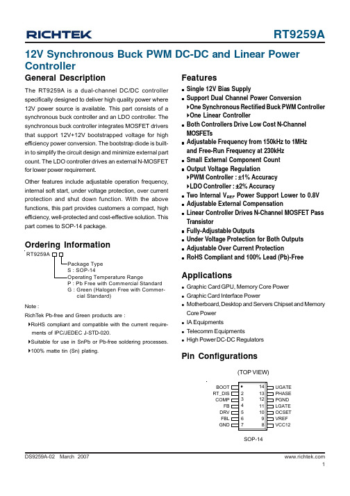
DS9259A-02 March 2007Featuresz Single 12V Bias SupplyzSupport Dual Channel Power Conversion`One Synchronous Rectified Buck PWM Controller `One Linear ControllerzBoth Controllers Drive Low Cost N-Channel MOSFETszAdjustable Frequency from 150kHz to 1MHz and Free-Run Frequency at 230kHz z Small External Component Count zOutput Voltage Regulation`PWM Controller : ±1% Accuracy `LDO Controller : ±2% Accuracyz Two Internal V REF Power Support Lower to 0.8V z Adjustable External CompensationzLinear Controller Drives N-Channel MOSFET Pass TransistorzFully-Adjustable Outputsz Under Voltage Protection for Both Outputs z Adjustable Over Current ProtectionzRoHS Compliant and 100% Lead (Pb)-FreeApplicationsz Graphic Card GPU, Memory Core Power z Graphic Card Interface PowerzMotherboard, Desktop and Servers Chipset and Memory Core Power z IA Equipmentsz Telecomm EquipmentszHigh Power DC-DC Regulators12V Synchronous Buck PWM DC-DC and Linear Power ControllerPin ConfigurationsOrdering InformationGeneral DescriptionThe RT9259A is a dual-channel DC/DC controller specifically designed to deliver high quality power where 12V power source is available. This part consists of a synchronous buck controller and an LDO controller. The synchronous buck controller integrates MOSFET drivers that support 12V+12V bootstrapped voltage for high efficiency power conversion. The bootstrap diode is built-in to simplify the circuit design and minimize external part count. The LDO controller drives an external N-MOSFET for lower power requirement.Other features include adjustable operation frequency,internal soft start, under voltage protection, over current protection and shut down function. With the above functions, this part provides customers a compact, high efficiency, well-protected and cost-effective solution. This part comes to SOP-14 package.(TOP VIEW)SOP-14FBL DRV COMPRT_DIS GNDPHASE FB VCC12VREF OCSET BOOT PGND UGATELGATE Note :RichTek Pb-free and Green products are :`RoHS compliant and compatible with the current require- ments of IPC/JEDEC J-STD-020.`Suitable for use in SnPb or Pb-free soldering processes.`100% matte tin (Sn) plating.RT9259AP : Pb Free with Commercial Standard G : Green (Halogen Free with Commer- cial Standard)Typical Application CircuitVOUT1V OUT2C V CC +12VDS9259A-02 March 2007Functional Pin DescriptionBOOT (Pin 1)Bootstrap supply for the upper gate driver. Connect the bootstrap capacitor between BOOT pin and the PHASE pin. The bootstrap capacitor provides the charge to turn on the upper MOSFET .RT_DIS (Pin 2)Connect a resistor from RT_DIS to GND to set frequency.In addition, if this pin is pulled down towards GND, it will disable both regulator outputs until P (Pin 3)Buck converter external compensation. This pin is used to compensate the control loop of the buck converter.FB (Pin 4)Buck converter feedback voltage. This pin is the inverting input of the PWM error amplifier. FB senses the switcher output through an external resistor divider network.DRV (Pin 5)Connect this pin to the gate of an external MOSFET . This pin provides the drive for the linear regulator ’s pass MOSFET .FBL (Pin 6)Linear regulator feedback voltage. This pin is the inverting input of the LDO error amplifier and protection monitor.Connect this pin to an external resistor divider network of the linear regulator.GND (Pin 7)Signal ground for the IC. All voltages levels are measured with respect to this pin.VCC12 (Pin 8)Connect this pin to a well-decoupled 12V bias supply. It is also the positive supply for the lower gate driver, LGATE.VREF (Pin 9)0.8V reference voltage output.OCSET (Pin 10)Connecting a resistor (R OCSET ) from this pin to the source of the upper MOSFET and the drain of the lower MOSFET sets the over-current trip point. R OCSET , an internal 40μA current source, and the lower MOSFET on resistance,R DS(ON), set the converter over-current trip point (I OCSET )according to the following Equation : MOSFETlower the of 0.4VR 40uA I DS(ON)OCSET OCSET R −×=LGATE (Pin 11)Lower gate driver output. Connect to the gate of the low-side power N-Channel MOSFET . This pin is monitored by the adaptive shoot-through protection circuitry to determine when the lower MOSFET has turn off.PGND (Pin 12)Power ground return for the lower gate driver.PHASE (Pin 13)Connect this pin to the source of the upper MOSFET and the drain of the lower MOSFET . This pin is monitored by the adaptive shoot-through protection circuitry to determine when the upper MOSFET has turned off.UGATE (Pin 14)Upper gate driver output. Connect to gate of the high-side power N-Channel MOSFET . This pin is monitored by the adaptive shoot-through protection circuitry to determine when the upper MOSFET has turned off.Function Block DiagramDS9259A-02 March 2007Electrical CharacteristicsTo be continuedAbsolute Maximum Ratings (Note 1)zSupply Voltage, V CC --------------------------------------------------------------------------------------15V z PHASE to GNDDC -------------------------------------------------------------------------------------------------------------−5V to 15V < 200ns ------------------------------------------------------------------------------------------------------−10V to 30V z BOOT to PHASE ------------------------------------------------------------------------------------------15V z BOOT to GNDDC -------------------------------------------------------------------------------------------------------------−0.3V to V CC +15V < 200ns ------------------------------------------------------------------------------------------------------−0.3V to 42Vz UGATE -------------------------------------------------------------------------------------------------------V PHASE − 0.3V to V BOOT + 0.3V z LGATE -------------------------------------------------------------------------------------------------------GND − 0.3V to V CC + 0.3V z DRV ----------------------------------------------------------------------------------------------------------GND − 0.3V to V CC + 0.3V z Input, Output or I/O Voltage -----------------------------------------------------------------------------GND − 0.3V to 7V z Power Dissipation, P D @ T A = 25°CSOP-14------------------------------------------------------------------------------------------------------1.000W z Package Thermal Resistance (Note 4)SOP-14, θJA -------------------------------------------------------------------------------------------------100°C/W z Junction T emperature -------------------------------------------------------------------------------------150°C z Lead Temperature (Soldering, 10 sec.)---------------------------------------------------------------260°C z Storage T emperature Range ----------------------------------------------------------------------------−40°C to 150°C z ESD Susceptibility (Note 2)HBM (Human Body Mode)------------------------------------------------------------------------------2kV MM (Machine Mode)--------------------------------------------------------------------------------------200VRecommended Operating Conditions (Note 3)z Supply Voltage, V CC --------------------------------------------------------------------------------------12V ± 10%z Junction T emperature Range ----------------------------------------------------------------------------−40°C to 125°C zAmbient T emperature Range ----------------------------------------------------------------------------−40°C to 85°CNote 1. Stresses listed as the above "Absolute Maximum Ratings"may cause permanent damage to the device. These are for stress ratings. Functional operation of the device at these or any other conditions beyond those indicated in the operational sections of the specifications is not implied. Exposure to absolute maximum rating conditions for extended periods may remain possibility to affect device reliability.Note 2. The device is not guaranteed to function outside its operating conditions.Note 3.θJA is measured in the natural convection at T A = 25°C on a low effective thermal conductivity test board of JEDEC 51-3 thermal measurement standard.Note 4.θJA is measured in the natural convection at T A = 25°C on a high effective 4-layers 2S2P thermal conductivity test board of JEDEC 51-7 thermal measurement standard.DS9259A-02 March 2007Typical Operating CharacteristicsStart UpTime (1ms/Div)(500mV/Div)(10V/Div)(5V/Div)(500mV/Div)No LoadRT_DisPHASE V IN1V OUT1Shut DownTime (5μs/Div)(500mV/Div)(20V/Div)RT_DisLGATEUGATEV OUT1(10V/Div)(1V/Div)Full LoadDead TimeTime (25ns/Div)No Load, RisingPHASELGATEUGATE(5V/Div)V IN1Dead TimeTime (25ns/Div)No Load, FallingPHASELGATEUGATE(5V/Div)V IN1Power OffTime (5μs/Div)(0.5A/Div)(10V/Div)I LLGATEUGATEV REF(10V/Div)(200mV/Div)No Load OCPTime (2.5ms/Div)I L(10A/Div)V OUT1(2V/Div)Start UpTime (1ms/Div)(500mV/Div)V OUT1(2.5A/Div)I LOADNo LoadStart UpTime (1ms/Div)(500mV/Div)V OUT1RT_Dis(500mV/Div)I Load = 20AUnder Voltage ProtectionTime (10ms/Div)(10V/Div)LDO COMPLGATEUGATEV OUT2(1V/Div)(20V/Div)(500mV/Div)V IN2 = 0VTransient Response Time (2.5μs/Div)I LV OUT1UGATE(100mV/Div)(10A/Div)(20V/Div)V IN1 = 12V, V OUT1 = 2V I LOAD1 = 1A to 20ATransient ResponseTime (10μs/Div)I LV OUTUGATE(100mV/Div)(10A/Div)(20V/Div)V IN1 = 12V, V OUT1 = 2V I LOAD1 = 20A to 1ATransient ResponseTime (100μs/Div)I LV OUT2(2mV/Div)(0.5A/Div)LDOV IN2 = 12V, V OUT2 = 2.5V I LOAD = 1A to 100mADS9259A-02 March 2007Application InformationIntroductionThe RT9259A is a dual-channel DC/DC controller specifically designed to deliver high quality power where 12V power source is available. This part consists of a synchronous buck controller and an LDO controller. The synchronous buck controller integrates internal MOSFET drivers that support 12V+12V bootstrapped voltage for high efficiency power conversion. The bootstrap diode is built-in to simplify the circuit design and minimize external part count. The LDO controller drives an external N-MOSFET for lower power requirement.Internal 5VDD RegulatorIt is highly recommended to power the RT9259A with well-decoupled 12V to VCC12 pin. VCC12 powers the RT9259A control circuit, low side gate driver and bootstrap circuit for high side gate driver. A bootstrap diode is embedded to facilitates PCB design and reduce the total BOM cost. No external Schottky diode is required. The RT9259A integrates MOSFET gate drives that are powered from the VCC12 pin and support 12V + 12V driving capability.Converters that consist of RT9259A feature high efficiency without special consideration on the selection of MOSFETs.An internal linear regulator regulates VCC12 input to a 5VDD voltage for internal control logic circuit. No external bypass capacitor is required for filtering the 5VDD voltage.This further facilitates PCB design and reduces the total BOM cost.Power On ResetThe RT9259A automatically initializes up on applying of inp ut power (at the VCC12) pin. The power on reset function (POR) continually monitors the input bias supply voltage at the VCC12 pin. The VCC12V POR level is typically 9.6V at VCC12V rising.Frequency Setting and Shut DownConnecting a resistor R RT from the RT_DIS pin to GND sets the operation frequency. The relation can be roughly expressed in the equation.When let open, the free running frequency is 230kHz typically. Figure 1 shows the operation frequency vs. R RT for quick reference.Figure 1. RT vs. fsw at Low FrequencyShorting the RT_DIS pin to GND with an external signal-level MOSFET shuts down the device. This allows flexiblepower sequence control for specified application. The RT_DIS pin threshold voltage is 0.4V typically.VIN1 DetectionThe RT9259A continuously generates a 10kHz pulse train with 1μs pulse width to turn on the upper MOSFET for detecting the existence of VIN1 after VCC12V POR and RT_DIS enabled as shown in Figure 2. PHASE pin voltage is monitored during the detection duration.If the PHASE voltage crosses 1.5V four times, VIN1existence is recognized and the RT9259A initiates its soft start cycle as described in next section.(kHz)R 7700kHz 302f RTOSC +≅0200400600800100012001400101001000R RT (kohm)f S W (k H z)(k Ω)Figure 2V IN1PHASEInternal Counter will count (V PHASE > 1.5V)four times (rising & falling) to recognize V IN1 is ready.1st 2nd 3rd 4th PHASEwaveformSoft Start for Synchronous Buck ConverterA built-in soft-start is used to prevent surge current from power supply input during power on (referring to the Functional Block Diagram). The error amplifier EA is a three-input device. SSE or V REF1 whichever is smaller dominates the behavior non-inver ting input. The internal soft start voltage SSE linearly ramps up to about 4V after VIN1existence is recognized with about 2ms delay. Accordin g,the output voltage ramps up smoothly to its target level.The rise time of output voltage is about 2ms as shown in Figure 3. V REF1 takes over the behavior EA when SSE >V REF1.SSE is also used for LDO soft start. LDO input voltage VIN2 MUST be ready before SSE starts to ramp up.Otherwise UVP function of LDO may be triggered and shut down the RT9259A.Figure 3 : Start up by RT_DISUnder Voltage ProtectionThe voltages at FB and FBL pin are monitored for under voltage protection (UVP) after the soft start is completed.UVP is triggered if one of the feedback voltages is under (50% x V REFX ) with a 30us delay. As shown in Figure 4,the RT9259A PWM controller is shut down when V FB drops lower than the UVP threshold. In Figure 5, the RT9259A shuts down after 4 time UVP hiccups triggered by FBL.Figure 4. UVP triggered by FBFigure 5. UVP hiccups triggered by FBLOver Current ProtectionThe RT9259A senses the current flowing through lower MOSFET for over current protection (OCP) by sensing the PHASE pin voltage as shown in the Functional Block Diagram. A 40uA current source flows through the external resistor R OCSET to PHASE pin causes 0.8V voltage drop across the resistor. OCP is triggered if the voltage at PHASE pin (drop of lower MOSFET V DS ) is lower than −0.4V when low side MOSFET conducting. Accordingly inductor current threshold for OCP is a function of conducting resistance of lower MOSFET R DS(ON) as :DS(ON)OCSET OCSET R 0.4V-R A 40I ×=μTime (10ms/Div)LGATE (10V/Div)V OUT1(1V/Div)UGATE (20V/Div)COMP (500mV/Div)V IN2 = 0VTime (1ms/Div)RT_DIS (500mV/Div)UGATE (20V/Div)V OUT1(500mV/Div)LGATE (10V/Div)Time (10ms/Div)FB(500mV/Div)UGATE (20V/Div)V OUT (20V/Div)V IN1 = 12V to 0V11DS9259A-02 March 2007If MOSFET with R DS(ON) = 16m Ω is used, the OCP threshold current is about 25A. Once OCP is triggered,the RT9259A enters hiccup mode and re-soft starts again.The RT9259A shuts down after 4 time OCP hiccups.Figure 6. Shorted then Start UpFigure 7. Shorted then Start Up (Extended Figure 3)Feedback CompensationThe RT9259A is a voltage mode controller. The control loop is a single voltage feedback path including a compensator and modulator as shown Figure 8. The modulator consists of the PWM comparator and power stage. The PWM comparator compares error amplifier EA output (COMP) with oscillator (OSC) sawtooth wave to provide a pulse-width modulated (PWM) with an amplitude of V IN at the PHASE node. The PWM wave is smoothed by the output filter L OUT and C OUT . The output voltage (V OUT )is sensed and fed to the inverting input of the error amplifier.Figure 8. Closed LoopTime (5μs/Div)UGATE (5V/Div)LGATE (5V/Div)I L(20A/Div)Time (2.5ms/Div)Inductor Current(20A/Div)A well-designed compensator regulates the output voltage to the reference voltage V REF with fast transient response and good stability.In order to achieve fast transient response and accurate output regulation, an adequate compensator design is necessary. The goal of the compensation network is to provide adequate phase margin (greater than 45 degrees)and the highest 0dB crossing frequency. It is also recommended to manipulate loop frequency response that its gain crosses over 0dB at a slope of −20dB/dec.1) Modulator Frequency EquationsThe modulator transfer function is the small-signal transfer function of V OUT /V COMP (output voltage over the error amplifier output. This transfer function is dominated by a DC gain, a double pole, and a zero as shown in Figure 10.The DC gain of the modulator is the input voltage (V IN )divided by the peak to peak oscillator voltage V OSC . The output LC filter introduces a double pole, 40dB/decade gain slope above its corner resonant frequency, and a total phase lag of 180 degrees. The resonant frequency of the LC filter expressed as :OUTOUT LC C L 21f ×=π12DS9259A-02 March 2007 ESRC 21f OUT ESR ××=πThe ESR zero is contributed by the ESR associated with the output capacitance. Note that this requires that the output capacitor should have enough ESR to satisfy stability requirements. The ESR zero of the output capacitor expressed as follows :2) Compensation Frequency EquationsThe compensation network consists of the error amplifier and the impedance networks Z C and Z F as shown in Figure 9.Figure 9. Compensation LoopC2x R2 x 21f Z1π=C2C1C2x C1 x R2 x 21f P1+=πFigure 10 shows the DC-DC converter's gain vs. frequency.The compensation gain uses external impedance networks Z C and Z F to provide a stable, high bandwidth loop. High crossover frequency is desirable for fast transient response,but often jeopardize the system stability. In order to cancel one of the LC filter poles, place the zero before the LC filter resonant frequency. In the experience, place the zero at 75% LC filter resonant frequency. Crossover frequency should be higher than the ESR zero but less than 1/5 of the switching frequency. The second pole is placed at half the switching frequency.Figure 10. Bode PlotThermal ConsiderationsFor continuous operation, do not exceed absolutemaximum operation junction temperature 125°C. The maximum power dissipation depends on the thermal resistance of IC package, PCB layout, the rate of surroundings airflow and temperature difference between junction to ambient. The maximum power dissipation can be calculated by following formula :P D(MAX) = ( T J(MAX) − T A ) / θJAWhere T J(MAX) is the maximum operation junction temperature 125°C, T A is the ambient temperature and the θJA is the junction to ambient thermal resistance.The junction to ambient thermal resistance θJA is layout dependent. For SOP-14 packages, the thermal resistance θJA is 100°C/W on the standard JEDEC 51-7 four-layers thermal test board.The maximum power dissipation at T A = 25°C can be calculated by following formula :P D(MAX) = ( 125°C − 25°C) / 100°C/W = 1.000 W for SOP-14 packagesThe maximum power dissipation depends on operating ambient temperature for fixed T J(MAX) and thermal resistance θJA . For RT9259A packages, the Figure 11 of derating curves allows the designer to see the effect of rising ambient temperature on the maximum power allowed.Z OUT13DS9259A-02 March 2007PCB Layout ConsiderationsMOSFETs switch very fast and efficiently. The speed with which the current transitions from one device to another causes voltage spikes across the interconnecting impedances and parasitic circuit elements. The voltage spikes can degrade efficiency and radiate noise, that results in over-voltage stress on devices. Careful component placement layout and printed circuit design can minimize the voltage spikes induced in the converter. Consider, as an example, the turn-off transition of the upper MOSFET prior to turn-off, the upper MOSFET was carrying the full load current. During turn-off, current stops flowing in the upper MOSFET and is picked up by the low side MOSFET or schottky diode. Any inductance in the switched current path generates a large voltage spike during the switching interval. Careful component selections, layout of the critical components, and use shorter and wider PCB traces help in minimizing the magnitude of voltage spikes.There are two sets of critical components in a DC-DC converter using the RT9259A. The switching power components are most critical because they switch large amounts of energy, and as such, they tend to generate equally large amounts of noise. The critical small signal components are those connected to sensitive nodes or those supplying critical bypass current.Figure 12. The connections of the critical components inthe converterThe power components and the PWM controller should be placed firstly. Place the input capacitors, especially the high-frequency ceramic decoupling capacitors, close to the power switches. Place the output inductor and output capacitors between the MOSFET s and the load. Also locate the PWM controller near by MOSFET s. A multi-layer printed circuit board is recommended. Figure 12 shows the connections of the critical components in the converter.Note that the capacitors C IN and C OUT each of them represents numerous physical capacitors.Use a dedicated grounding plane and use vias to ground all critical components to this layer. Apply another solid layer as a power plane and cut this plane into smaller islands of common voltage levels. The power plane should support the input power and output power nodes. Use copper filled polygons on the top and bottom circuit layers for the PHASE node, but it is not necessary to oversize this particular island. Since the PHASE node is subjected to very high dV/dt voltages, the stray capacitance formed betweenthese islands and the surrounding circuitry will tend to couple switching noise. Use the remaining printed circuit layers for small signal routing. The PCB traces between the PWM controller and the gate of MOSFET and also the traces connecting source of MOSFETs should be sized to carry 2A peak currents.Figure 11. Derating Curves for RT9259A Packages00.20.40.60.811.2255075100125Ambient Temperature M a x i m u m P o w e r D i s s i p a t i o n (W )(°C)14DS9259A-02 March 2007Richtek Technology CorporationHeadquarter5F, No. 20, Taiyuen Street, Chupei City Hsinchu, Taiwan, R.O.C.Tel: (8863)5526789 Fax: (8863)5526611Richtek Technology CorporationTaipei Office (Marketing)8F, No. 137, Lane 235, Paochiao Road, Hsintien City Taipei County, Taiwan, R.O.C.Tel: (8862)89191466 Fax: (8862)89191465Email: marketing@Outline DimensionM14–Lead SOP Plastic Package。

Dual Output TypesRxxG055/12±5±1007127RxxG095/12±9±557435DIP14 RxxG125/12±12±427542RxxG155/12±15±337641RxxG0524/48±5±10080/7045RxxG0924/48±9±557052/58DIP14 RxxG1224/48±12±427065/68RxxG1524/48±15±337070/75RxxH055/12±5±1007127RxxH095/12±9±557435SIP7 RxxH125/12±12±427542RxxH155/12±15±337641RxxH0524/48±5±10070/8045RxxH0924/48±9±557052/58SIP7 RxxH1224/48±12±427065/68RxxH1524/48±15±337070/75Absolute Maximum RatingsInput Voltage V IN5V types 7V typ.12V types 15V typ.24V types 24V typ.48V types48V typ.Short Circuit Duration 1)1s Internal Power Dissipation560mW Lead Temperature (1.5 mm from case for 10 seconds)300 °C1).Supply voltage must be discontinued at the end of the short circuit duration.Input Voltage Range V IN (continuous operation)5V input types 4.5VDC min./ 5.5VDC max.12V input types 10.8VDC min./ 13.2VDC max.24V input types 28VDC max.48V input types54VDC max.Reflected Ripple Current (depending on the type)20 mA p-p min.to 40 mA p-p max.Voltage Set Point Accuracy See Tolerance EnvelopeLine Regulation1.0% / 1.2% of V INLoad Voltage Regulation (10% load to 100% full load)single output types 6.7% min./ 15% max.dual output types 6.8% min./ 10% max.Ripple & Noise (20MHz band limited)single output types 32mVp-p min./ 80mVp-p max.dual output types24mVp-p min./ 40mVp-p max.Isolation Voltage (for 1 minute)3000VDC min.Test Voltage (50Hz,10 seconds)3000 Vpk min.Resistance (Viso = 1000V)10 G Ωtyp.Switching Frequency at Full Load (depending on the type)V IN 5V output types 120kHz min./ 135kHz max.V IN 12V output types 150kHz min./ 170kHz max.V IN 24V output types 150kHz max.V IN 48V output types150kHz max.Package Weight2.11 gOperating Temperature Range (all output types)–40°C min.to +85°C max.(see graph)Storage Temperature Range–50°C min.+125°C max.Case Temperature Above Ambient (depending on the type)5V output types+28°C max.all other output types +25°C max.MTTF 1) (depending on the type)–40°C,single output types 303kHrs min./ 2938kHrs max.+25°C,single output types 252kHrs min./ 2414kHrs max.+85°C,single output types 212kHrs min./ 1961kHrs max.–40°C,dual output types 185kHrs min./ 2068kHrs max.+25°C,dual output types 154kHrs min./ 1697kHrs max.+85°C,dual output types130kHrs min./ 1368kHrs max.1).Calculated using MIL-HDBK-217F with nominal input voltage at full load.Please contact us,if you need exact parameters for the converter you have selected.Electrical Specifications (measured at T A = 25°C,at nominal input voltage and rated output current unless otherwise specified)Package Style and Pinning (mm)。
1000VDC I/O isolation Internal SMD technology Built-in EMI filterCooling by free air convection Non-conductive plastic case Dual in line package SIP packge is available 100% burn-in testLow cost / High reliability 2 years warrantySPECIFICATIONSELECTION GUIDEFile Name: SRS-SPEC 2008-05-08SRS-050560%0 ~ 100mA 5V SRS-1205ORDER NO.DC VOLTAGECURRENT RANGE EFFICIENCY (TYP.)RATED POWEROUTPUTOUTPUTOUTPUTSWITCHING FREQUENCYNORMAL VOLTAGEINPUT CURRENT INPUT(Note. 4)ENVIRONMENT SAFETY &EMCWITHSTAND VOLTAGEISOLATION RESISTANCE ISOLATION CAPACITANCEWORKING TEMP.WORKING HUMIDITYSTORAGE TEMP., HUMIDITY TEMP. COEFFICIENTVIBRATION MTBFDIMENSION OTHERS NOTEWEIGHTOVERLOADFILTER SHORT CIRCUIT PROTECTION150 ~ 350% rated output powerAll output equipped with short circuitI/P-O/P:1KVDC I/P-O/P: 100M Ohms /500VDC / 25/ 70% RH80pF max.600khrs min. MIL-HDBK-217F(25)-25 ~ +71(Refer to output load derating curve)20% ~ 90% RH non-condensing-25 ~ +105, 10 ~ 95% RH0.03% /(0 ~ 50)10~500Hz,2G 10min./1cycle,period for 60min.each along X,Y,Z axes22.6*9.9*8.4mm or 0.89"*0.39"*0.33" inch (L*W*H)3.1g 1.All parameters are specified at normal input, rated load, 2570% RH ambient.2.Ripple & noise are measured at 20MHz by using a 12" twisted pair terminated with a 0.1uf & 47uf capacitor.3.Load regulation is measured from 10% to 100% rated load.4.Please prevent the converter from operating in overload or short circuit condition for more than 30 seconds.Full load No load Capacitor type Mechanical SpecificationUnit: mm (inch)Pin ConfigurationDerating Curve9.9 (0.39)16 111 610 79 87.62 (0.30)3.81 (0.15)12.7 (0.50)0.5 (0.02)2.54 (0.10)8.4 (0.33)22.6 (0.89)BOTTOM VIEWOutput+Vin -Vout+Vout -VinPin No.1 & 166 & 117 & 108 & 9SRS-2412SRS-4812SRS-051560%0 ~ 34mA 15V SRS-1215SRS-2415SRS-481518mA 6mA48V SRS-051260%SRS-1212ORDER NO.DC VOLTAGECURRENT RANGE EFFICIENCY (TYP.)32mA 8mA24V 18mA 6mA48V 166mA 12mA5V 66mA 10mA12V 32mA 8mA24V 0 ~ 42mA 12V 166mA 12mA5VVOLTAGE RANGE 43.2 ~ 52.8V 21.6 ~ 26.4V 43.2 ~ 52.8V 4.5 ~ 5.5V 10.8 ~ 13.2V 21.6 ~ 26.4V 4.5 ~ 5.5V 50KHz min.1.0%1.0%2.0%(Typ.) 3.0%(max.)100mVp-p0.5W10.8 ~ 13.2V 66mA 10mA12V Features :Protection type : Hiccup mode, recovers automatically after fault condition is removed Protection type :Hiccup mode, recovers automatically after fault condition is removed Ta ()L O A D (%)-2502550716080100100SRS-2405SRS-4805SRS-050960%0 ~ 56mA 9V SRS-1209SRS-2409SRS-48090.5W DC-DC Regulated Single Output ConverterSRSseriesRIPPLE & NOISE (max.)Note.2LINE REGULATION LOAD REGULATION Note.3VOLTAGE ACCURACY PROTECTION Fuse recommended元器件交易网。
●Wide Temperature Performance at full 1 Watt Load,–40°C to +85°C ●1kVDC Isolation●Industry Standard Pinout ●Efficiency to 80%●UL 94V-O Package Material ●Internal SMD Construction ●Toroidal Magnetics●MTTF up to 2.9 Million HoursFeaturesAbsolute Maximum RatingsInput Voltage V IN 5V types 7V Input Voltage V IN 12V types 15V Short Circuit Duration 1)1s Internal Power Dissipation450mW Lead Temperature (1.5 mm from case for 10 seconds)300 °C1).Supply voltage must be discontinued at the end of the short circuit duration.Electrical Specifications (measured at T A = 25°C,at nominal input voltage and rated output current unless otherwise specified)Input Voltage Range V IN(continuous operation)5V input types 4.5VDC min./ 5.5VDC max.12V input types10.8VDC min./ 13.2VDC max. Reflected Ripple Current (depending on the type)26 mA p-p min.to 48 mA p-p max. Voltage Set Point Accuracy See Tolerance Envelope Line Regulation 1.0% / 1.2% of V IN Load Voltage Regulation (10% load to 100% full load)5V output types14% min./ 15% max.9V output types9% min./ 10% max.12V output types7.5% min./ 9.5% max.15V output types7% min./ 8.5% max. Ripple & Noise (20MHz band limited),(depending on the type)40mVp-p min./ 110mVp-p max. Isolation Voltage (flash tested for 1 second)1000VDC min. Test Voltage (50Hz,10 seconds)1000 Vpk min. Resistance (Viso = 500V)10 GΩtyp. Switching Frequency at Full Load V IN 5V input types110kHz typ.V IN 12V input types145kHz typ. Package Weight SIP types 1.30 gDIP types 1.48 g Operating Temperature Range (all output types)–40°C min.to +85°C max.(see graph) Storage Temperature Range–50°C min.+130°C max. Case Temperature Above Ambient (depending on the type)5V output types+41°C max.all other output types+32°C max. MTTF 1) (depending on the type)–40°C302kHrs min./ 2938kHrs max.+25°C252kHrs min./ 2414kHrs max.+85°C212kHrs min./ 1961kHrs max.1).Calculated using MIL-HDBK-217F with nominal input voltage at full load.Please contact us,if you need exact parameters for the converter you have selected.Typical Characteristics,Tolerance Envelope and Temperature Derating GraphPackage Style and Pinning (mm)。