APT1608EC, 规格书,Datasheet 资料
- 格式:pdf
- 大小:247.50 KB
- 文档页数:5

Kingbright 今台台湾kingbright代理今台供应商优势供应KPT系列,KP系列,KPTB系列,KPTD系列,KPHHS系列,KPHCM系列, 今台LED 深圳现货供应大量库存Kingbright 今台LED 发光二极管KP-1608SGCKingbright 今台LED 发光二极管KP-1608SURCKKingbright 今台LED 发光二极管KP-1608SYCKKingbright 今台LED 发光二极管KP-1608VBC-DKingbright 今台LED 发光二极管KP-1608ZGCKingbright 今台LED 发光二极管KP-2012CGCKKingbright 今台LED 发光二极管KP-2012F3CKingbright 今台LED 发光二极管KP-2012F3CKingbright 今台LED 发光二极管KP-2012QBC-DKingbright 今台LED 发光二极管KP-2012SECKKingbright 今台LED 发光二极管KP-2012SF4CKingbright 今台LED 发光二极管KP-2012SF4CKingbright 今台LED 发光二极管KP-2012SGCKingbright 今台LED 发光二极管KP-2012SURCKKingbright 今台LED 发光二极管KP-2012SYCKKingbright 今台LED 发光二极管KPT-2012QBC-DKingbright 今台LED 发光二极管KPT-2012SECKKingbright 今台LED 发光二极管KPT-2012SGCKingbright 今台LED 发光二极管KPT-2012SURCKKingbright 今台LED 发光二极管KPT-2012SYCKKingbright 今台LED 发光二极管KPT-2012VBC-DKingbright 今台LED 发光二极管KPT-2012ZGCKingbright 今台LED 发光二极管KPT-3216CGCKKingbright 今台LED 发光二极管KPT-3216QBC-DKingbright 今台LED 发光二极管KPT-3216SECKKingbright 今台LED 发光二极管KPT-3216SGCKingbright 今台LED 发光二极管KPT-3216SURCKKingbright 今台LED 发光二极管KPT-3216SYCKKingbright 今台LED 发光二极管KPT-3216VBC-DKingbright 今台LED 发光二极管KPT-3216ZGCKingbright 今台LED 发光二极管KPTB-1612QBDSEKCKingbright 今台LED 发光二极管KPTB-1612SURKCGKCKingbright 今台LED 发光二极管KPTB-1612SURKQBDCKingbright 今台LED 发光二极管KPTB-1612SYKCGKCKingbright 今台LED 发光二极管KPTB-1615SURKCGKCKingbright 今台LED 发光二极管KPTB-1615SURKQBDCKingbright 今台LED 发光二极管KPTB-1615SYKCGKCKingbright 今台LED 发光二极管KPTD-1608CGCKKingbright 今台LED 发光二极管KPTD-1608QBC-DKingbright 今台LED 发光二极管KPTD-1608QBC-GKingbright 今台LED 发光二极管KPTD-1608SECKKingbright 今台LED 发光二极管KPTD-1608SURCK Kingbright 今台LED 发光二极管KPTD-1608SYCK Kingbright 今台LED 发光二极管KPTD-1608VBC-D Kingbright 今台LED 发光二极管KPTD-1608ZGC Kingbright 今台LED 发光二极管KPTD-1608ZGC-G Kingbright 今台LED 发光二极管KPTD-3216CGCK Kingbright 今台LED 发光二极管KPTD-3216QBC-D Kingbright 今台LED 发光二极管KPTD-3216SECK Kingbright 今台LED 发光二极管KPTD-3216SURCK Kingbright 今台LED 发光二极管KPTD-3216SYCK Kingbright 今台LED 发光二极管KPTD-3216VBC-D Kingbright 今台LED 发光二极管KPTD-3216ZGC Kingbright 今台LED 发光二极管KPTD-3216ZGC-G Kingbright 今台LED 发光二极管KPTL-3216CGCK Kingbright 今台LED 发光二极管KPTL-3216QBC-D Kingbright 今台LED 发光二极管KPHCM-2012CGCK Kingbright 今台LED 发光二极管KPHCM-2012QBC-D Kingbright 今台LED 发光二极管KPHCM-2012SECK Kingbright 今台LED 发光二极管KPHCM-2012SURCK Kingbright 今台LED 发光二极管KPHCM-2012SYCK Kingbright 今台LED 发光二极管KPHCM-2012VBC-D Kingbright 今台LED 发光二极管KPHCM-2012ZGC Kingbright 今台LED 发光二极管KPHHS-1005CGCK Kingbright 今台LED 发光二极管KPHHS-1005QBC-D-V Kingbright 今台LED 发光二极管KPHHS-1005SECK Kingbright 今台LED 发光二极管KPHHS-1005SURCK Kingbright 今台LED 发光二极管KPHHS-1005SYCK Kingbright 今台LED 发光二极管KPHHS-1005ZGC-V。

•All specifications are subject to change without notice.•Conformity to RoHS Directive: This means that, in conformity with EU Directive 2002/95/EC, lead, cadmium, mercury, hexavalent chromium, and specific bromine-based flame retardants, PBB and PBDE, have not been used, except for exempted applications.Inductors for High-frequency CircuitsMultilayer/STD MLG seriesType:Issue date:MLG0603S 0603[0201 inch]*MLG1005S 1005[0402 inch]MLG16081608[0603 inch]* Dimensions Code JIS[EIA]November 2011Inductors for High-frequency Circuits Multilayer/STDMLG Series MLG0603SFEATURES•Inductance values are supported from 0.3 to 180nH.•Advanced monolithic structure is formed using a multilayering and sintering process with ceramic and conductive materials for high-frequency.•The products contain no lead and also support lead-free soldering.•It is a product conforming to RoHS directive.APPLICATIONSFor high-frequency applications including mobile phones, high frequency modules (PA, VCO, FEM etc.), Bluetooth, W-LAN, UWB and tuners.SHAPES AND DIMENSIONSRECOMMENDED PC BOARD PATTERNRECOMMENDED SOLDERING CONDITION REFLOW SOLDERINGPRODUCT IDENTIFICATION (1) Series name (2) Dimensions L ×W(3) Type name (4) Inductance(5) Tolerance(6) Packaging style(7) TDK internal codeSPECIFICATIONSPACKAGING STYLE AND QUANTITIESHANDLING AND PRECAUTIONS•Before soldering, be sure to preheat components.The preheating temperature should be set so that thetemperature difference between the solder temperature and product temperature does not exceed 150°C.•After mounting components onto the printed circuit board, do not apply stress through board bending or mishandling.•When hand soldering, apply the soldering iron to the printed circuit board only. T emperature of the iron tip should not exceed 350°C. Soldering time should not exceed 3 seconds.Conformity to RoHS DirectiveMLG 0603S 2N2S T (1)(2)(3)(4)(5)(6)(7)06030.6×0.3mm (L ×W)2N2 2.2nH 12N 12nH R10100nHB ±0.1nHC ±0.2nH S ±0.3nH H ±3%J±5%TTaping (reel)Operating temperature range –55 to +125°CStorage temperature range–55 to +125°C(After mount)Packaging style QuantityT aping 15000 pieces/reel•Please contact our Sales office when your application is considered the following:The device’s failure or malfunction may directly endanger human life (e.g. application for automobile/aircraft/medical/nuclear power devices, etc.)•Conformity to RoHS Directive: This means that, in conformity with EU Directive 2002/95/EC, lead, cadmium, mercury, hexavalent chromium, and specific bromine-based flame retardants, PBB and PBDE, have not been used, except for exempted applications.ELECTRICAL CHARACTERISTICS∗ : Please specify inductance tolerance, B (±0.1nH), C (±0.2nH), S (±0.3nH), H (±3%) or J (±5%).Please contact us for information on inductance tolerance, G(±2%).•T est equipmentInductance Q : HP4291A+16197A, or equivalentSRF: HP8720C, or equivalentRdc: YOKOGAWA TYPE7561, or equivalentInductance (nH)Inductance tolerance Q min.T est frequency L, Q (MHz)Self-resonant frequency (GHz)DC resistance(Ω)Rated current (mA)max.Part No.∗0.3±0.1, ±0.2nH —10010.020 up 0.10.02600MLG0603S0N3 T 0.4±0.1, ±0.2nH —10010.020 up 0.10.02 600MLG0603S0N4 T 0.5±0.1, ±0.2nH —10010.020 up 0.10.02 600MLG0603S0N5 T 0.6±0.1, ±0.2nH —10010.020 up 0.10.02 600MLG0603S0N6T 0.7±0.1, ±0.2nH —10010.016.3 0.10.02 600MLG0603S0N7T 1.0±0.1, ±0.2, 0.3nH 410010.014.4 0.10.04 600MLG0603S1N0 T 1.1±0.1, ±0.2, 0.3nH 410010.013.6 0.150.04 550MLG0603S1N1 T 1.2±0.1, ±0.2, 0.3nH 410010.012.3 0.150.06 550MLG0603S1N2 T 1.3±0.1, ±0.2, 0.3nH 41009.0 11.4 0.150.07 550MLG0603S1N3T 1.5±0.1, ±0.2, 0.3nH 41009.0 10.4 0.150.07 550MLG0603S1N5T 1.8±0.1, ±0.2, 0.3nH 41008.5 10.0 0.20.12 500MLG0603S1N8 T 2.0±0.1, ±0.2, 0.3nH 41008.2 9.8 0.250.14 400MLG0603S2N0 T 2.2±0.1, ±0.2, 0.3nH 41008.0 8.9 0.250.14 400MLG0603S2N2 T 2.4±0.1, ±0.2, 0.3nH 41008.0 9.2 0.250.15 300MLG0603S2N4 T 2.7±0.1, ±0.2, 0.3nH 4100 6.5 8.1 0.250.15300MLG0603S2N7T 3.0±0.1, ±0.2, 0.3nH 4100 6.2 7.8 0.30.20 300MLG0603S3N0T 3.6±0.1, ±0.2, 0.3nH 4100 5.5 6.9 0.350.22 300MLG0603S3N6 T 3.9±0.1, ±0.2, 0.3nH 5100 5.0 6.6 0.40.27 300MLG0603S3N9 T 4.3±3%, ±0.3nH 5100 5.0 6.4 0.40.27 300MLG0603S4N3 T 4.7±3%, ±0.3nH 5100 4.5 5.4 0.450.28 300MLG0603S4N7T 5.1±3%, ±0.3nH 5100 4.5 5.5 0.450.23 250MLG0603S5N1T 6.8±3, ±5%5100 3.6 4.4 0.60.32 250MLG0603S6N8 T 7.5±3, ±5%5100 4.2 5.3 0.70.43 200MLG0603S7N5 T 8.2±3, ±5%5100 3.8 4.5 0.70.45 200MLG0603S8N2 T 9.1±3, ±5%5100 3.4 4.9 0.80.51 200MLG0603S9N1T 10±3, ±5%5100 3.2 4.1 0.80.53 200MLG0603S10N T 12±3, ±5%6100 2.8 3.6 0.90.63 180MLG0603S12N T 13±3, ±5%6100 2.7 3.4 0.90.60 180MLG0603S13N T 15±3, ±5%6100 2.5 3.3 1.10.69 180MLG0603S15N T 16±3, ±5%6100 2.3 3.0 1.10.70 180MLG0603S16N T 18±3, ±5%6100 2.2 2.8 1.20.78 150MLG0603S18N T 20±3, ±5%6100 2.1 2.6 1.20.75150MLG0603S20N T 24±3, ±5%6100 1.9 2.3 1.30.90 150MLG0603S24N T 27±3, ±5%6100 1.8 2.2 1.5 1.00 100MLG0603S27N T 30±3, ±5%6100 1.6 2.0 1.60.95100MLG0603S30N T 33±3, ±5%6100 1.6 2.0 1.8 1.20 100MLG0603S33N T 36±3, ±5%6100 1.5 1.82.0 1.6850MLG0603S36N T 47±3, ±5%6100 1.3 1.5 2.2 1.48 50MLG0603S47N T 51±3, ±5%5100 1.2 1.5 2.8 1.9850MLG0603S51N T 56±3, ±5%5100 1.2 1.43.2 2.11 50MLG0603S56N T 62±3, ±5%5100 1.1 1.3 3.3 2.22 50MLG0603S62N T 68±3, ±5%5100 1.05 1.24 3.5 2.40 50MLG0603S68N T 82±3, ±5%51000.90 1.084.0 2.80 50MLG0603S82N T 91±3, ±5%51000.770.94 4.3 2.9750MLG0603S91N T 100±3, ±5%51000.77 0.94 4.5 3.13 50MLG0603SR10 T 110±3, ±5%51000.770.94 6.55.2450MLG0603SR11 T 120±3, ±5%51000.700.887.0 5.5350MLG0603SR12T 130±3, ±5%51000.670.847.3 5.6850MLG0603SR13T 160±3, ±5%51000.600.738.36.6750MLG0603SR16 T 180±3, ±5%51000.560.688.5 6.9950MLG0603SR18 TL, Q vs. FREQUENCY CHARACTERISTICSPart No.Inductance(nH)typ.Q typ.500MHz800MHz 1.8GHz 2.0GHz 2.4GHz500MHz800MHz 1.8GHz 2.0GHz 2.4GHzMLG0603S0N30.3 0.3 0.3 0.3 0.3 14min.18min.29min.32min.35min. MLG0603S0N40.4 0.4 0.4 0.4 0.4 14min.18min.29min.32min.35min. MLG0603S0N50.5 0.50.50.50.51418293235 MLG0603S0N60.6 0.6 0.5 0.5 0.5 16 20333439 MLG0603S0N70.7 0.6 0.6 0.6 0.6 1621333539 MLG0603S0N80.7 0.7 0.7 0.7 0.7 1520323438 MLG0603S0N90.8 0.8 0.8 0.8 0.8 1519303235 MLG0603S1N00.9 0.9 0.9 0.9 0.9 1418293034 MLG0603S1N1 1.0 1.0 1.0 1.0 1.0 14 19293134 MLG0603S1N2 1.1 1.1 1.1 1.1 1.1 1418293034 MLG0603S1N3 1.2 1.2 1.2 1.2 1.2 1418293033 MLG0603S1N5 1.4 1.4 1.4 1.4 1.4 1519293034 MLG0603S1N6 1.5 1.5 1.5 1.5 1.5 1418293033 MLG0603S1N8 1.7 1.7 1.7 1.7 1.7 1519293033 MLG0603S2N0 1.9 1.9 1.9 1.9 1.9 1418282932 MLG0603S2N2 2.1 2.0 2.1 2.1 2.1 1418272831 MLG0603S2N4 2.2 2.2 2.2 2.3 2.3 1418272932 MLG0603S2N7 2.5 2.5 2.6 2.6 2.7 1519282931 MLG0603S3N0 2.8 2.8 2.9 2.9 3.0 1519293133 MLG0603S3N3 3.1 3.1 3.2 3.3 3.4 15 19282931 MLG0603S3N6 3.4 3.4 3.5 3.6 3.7 1418262729 MLG0603S3N9 3.7 3.7 3.8 3.9 4.1 1519292932 MLG0603S4N3 4.1 4.1 4.3 4.4 4.6 1418272729 MLG0603S4N7 4.4 4.4 4.8 4.9 5.2 1520282930 MLG0603S5N1 4.8 4.8 5.1 5.3 5.6 1418252627 MLG0603S5N6 5.3 5.3 5.7 5.9 6.4 16 20272829 MLG0603S6N2 5.9 5.9 6.5 6.8 7.5 15 18252526 MLG0603S6N8 6.4 6.5 7.4 7.8 8.7 1519262625 MLG0603S7N57.1 7.1 7.8 8.0 8.7 14 18252626 MLG0603S8N27.8 7.8 8.8 9.3 10.4 15 18242424 MLG0603S9N18.6 8.6 9.8 10.3 11.5 1417222222 MLG0603S10N101012 12151518232221 MLG0603S11N10111314161518222220 MLG0603S12N11121415 1916 19242320 MLG0603S13N12131617221416191815 MLG0603S15N14152023331519201814 MLG0603S16N15162225371416161511 MLG0603S18N1718283514171513MLG0603S20N192032131614MLG0603S22N212340151713MLG0603S24N232445131513MLG0603S27N27291517MLG0603S30N29321315MLG0603S33N33361416MLG0603S36N36401415MLG0603S39N40471314MLG0603S43N44531414MLG0603S47N49 601313MLG0603S51N52641111MLG0603S56N597712 11MLG0603S62N66881110MLG0603S68N741041311MLG0603S75N82119108MLG0603S82N96161128MLG0603S91N1099MLG0603SR1012911MLG0603SR1113410MLG0603SR121569MLG0603SR131728MLG0603SR152237MLG0603SR162387MLG0603SR183186TYPICAL ELECTRICAL CHARACTERISTICSINDUCTANCE vs. FREQUENCY CHARACTERISTICSQ vs. FREQUENCY CHARACTERISTICSPACKAGING STYLES REEL DIMENSIONSTAPE DIMENSIONSInductors for High-frequency Circuits Multilayer/STDMLG Series MLG1005SFEATURES•Inductance values are supported from 0.3 to 390nH.•Advanced monolithic structure is formed using a multilayering and sintering process with ceramic and conductive materials for high-frequency.•The products contain no lead and also support lead-free soldering.•It is a product conforming to RoHS directive.APPLICATIONSFor high-frequency applications including mobile phones, high frequency modules (PA, VCO, FEM etc.), Bluetooth, W-LAN, UWB and tuners.SHAPES AND DIMENSIONSRECOMMENDED PC BOARD PATTERNRECOMMENDED SOLDERING CONDITION REFLOW SOLDERINGPRODUCT IDENTIFICATION (1) Series name (2) Dimensions(3) Type name (4) Inductance(5) Tolerance(6) Packaging style(7) TDK internal codeSPECIFICATIONSPACKAGING STYLE AND QUANTITIESHANDLING AND PRECAUTIONS•Before soldering, be sure to preheat components.The preheating temperature should be set so that thetemperature difference between the solder temperature and product temperature does not exceed 150°C.•After mounting components onto the printed circuit board, do not apply stress through board bending or mishandling.•When hand soldering, apply the soldering iron to the printed circuit board only. T emperature of the iron tip should not exceed 350°C. Soldering time should not exceed 3 seconds.Conformity to RoHS DirectiveMLG 1005S 2N2S T (1)(2)(3)(4)(5)(6)(7)10051.0×0.5mm (L ×W)2N2 2.2nH 12N 12nH R10100nHB ±0.1nHC ±0.2nH S ±0.3nH H ±3%J±5%TTaping (reel)Operating temperature range –55 to +125°CStorage temperature range–55 to +125°C(After mount)Packaging style QuantityT aping10000 pieces/reel•Please contact our Sales office when your application is considered the following:The device’s failure or malfunction may directly endanger human life (e.g. application for automobile/aircraft/medical/nuclear power devices, etc.)•Conformity to RoHS Directive: This means that, in conformity with EU Directive 2002/95/EC, lead, cadmium, mercury, hexavalent chromium, and specific bromine-based flame retardants, PBB and PBDE, have not been used, except for exempted applications.∗ : Please specify inductance tolerance, (B±0.1nH), (C±0.2nH), (S±0.3nH), (H±3%) or (J±5%).Please contact us for information on inductance tolerance, G(±2%).•T est equipmentInductance Q : HP4291A+16193A, or equivalentSRF: HP8720C, or equivalentRdc: YOKOGAWA TYPE7561, or equivalent(nH)tolerancemin.L, Q (MHz)(GHz)(Ω)(mA)max.Part No.∗min.typ.max.typ.0.3±0.1nH, ±0.2nH —10010.020up 0.10 0.01 1000MLG1005S0N3 T 0.4±0.1nH, ±0.2nH —10010.020up 0.10 0.01 1000MLG1005S0N4T 0.5±0.1nH, ±0.2nH —10010.020up 0.10 0.01 1000MLG1005S0N5 T 0.6±0.1nH, ±0.2nH —10010.0 20up 0.10 0.01 1000MLG1005S0N6 T 0.7±0.1nH, ±0.2nH —10010.018.7 0.10 0.02 1000MLG1005S0N7T 0.8±0.1nH, ±0.2nH —10010.0 16.40.10 0.021000MLG1005S0N8T 0.9±0.1nH,±0.2nH—10010.0 17.7 0.10 0.04 1000MLG1005S0N9 T 1.0±0.1nH, ±0.2, 0.3nH 710010.013.8 0.10 0.04 1000MLG1005S1N0 T 1.1±0.1nH, ±0.2, 0.3nH 710010.019.3 0.10 0.03 1000MLG1005S1N1T 1.2±0.1nH, ±0.2, 0.3nH 710010.011.6 0.10 0.04 1000MLG1005S1N2 T 1.3±0.1nH, ±0.2, 0.3nH 71008.00 11.7 0.10 0.04 1000MLG1005S1N3 T 1.5±0.1nH, ±0.2, 0.3nH 71008.00 9.6 0.10 0.06 1000MLG1005S1N5T 1.6±0.1nH, ±0.2, 0.3nH 71007.50 9.4 0.12 0.05 1000MLG1005S1N6 T 1.8±0.1nH, ±0.2, 0.3nH 71008.00 10.3 0.15 0.06 900MLG1005S1N8 T 2.0±0.1nH, ±0.2, 0.3nH 71007.50 9.3 0.15 0.07 900MLG1005S2N0T 2.2±0.1nH, ±0.2, 0.3nH 71007.00 8.6 0.15 0.08 900MLG1005S2N2T 2.4±0.1nH, ±0.2, 0.3nH 71007.00 8.2 0.15 0.08 800MLG1005S2N4 T 2.7±0.1nH, ±0.2, 0.3nH 7100 6.00 7.3 0.15 0.08 800MLG1005S2N7 T 3.0±0.1nH, ±0.2, 0.3nH 7100 5.50 6.8 0.20 0.09 800MLG1005S3N0T 3.3±0.1nH, ±0.2, 0.3nH 8100 5.00 6.1 0.20 0.09 800MLG1005S3N3 T 3.6±0.1nH, ±0.2, 0.3nH 8100 5.00 6.7 0.20 0.09 700MLG1005S3N6 T 3.9±0.1nH, ±0.2, 0.3nH 8100 5.00 6.5 0.20 0.11 700MLG1005S3N9T 4.3±0.2nH, ±0.3nH 8100 4.50 6.0 0.20 0.11 700MLG1005S4N3 T 4.7±0.2nH, ±0.3nH 8100 4.50 5.4 0.25 0.12 700MLG1005S4N7 T 5.1±0.2nH, ±0.3nH 8100 4.00 5.0 0.25 0.13 600MLG1005S5N1T 5.6±0.2nH, ±0.3nH 8100 4.00 5.3 0.25 0.14 600MLG1005S5N6T 6.2±3%, ±0.3nH 8100 4.00 4.7 0.25 0.16 600MLG1005S6N2 T 6.8±3%, ±5%8100 3.50 4.4 0.25 0.15 600MLG1005S6N8 T 7.5±3%, ±5%8100 3.00 4.1 0.25 0.15 500MLG1005S7N5T 8.2±3%, ±5%8100 3.00 4.0 0.30 0.19 500MLG1005S8N2 T 9.1±3%, ±5%8100 3.00 3.8 0.30 0.20 500MLG1005S9N1 T 10±3%, ±5%8100 2.50 3.4 0.35 0.22 500MLG1005S10N T 11±3%, ±5%8100 2.50 3.5 0.400.28400MLG1005S11N T 12±3%, ±5%8100 2.50 3.0 0.40 0.25400MLG1005S12N T 13±3%, ±5%8100 2.40 2.90.50 0.26400MLG1005S13N T 15±3%, ±5%8100 2.20 2.8 0.55 0.35400MLG1005S15N T 16±3%, ±5%8100 2.10 2.70.55 0.32400MLG1005S16N T 18±3%, ±5%8100 2.00 2.5 0.60 0.40 350MLG1005S18N T 20±3%, ±5%8100 1.90 2.40.60 0.38350MLG1005S20N T 22±3%, ±5%8100 1.70 2.2 0.70 0.46 350MLG1005S22N T 24±3%, ±5%8100 1.70 2.1 0.70 0.43350MLG1005S24N T 27±3%, ±5%8100 1.60 2.0 0.80 0.53 300MLG1005S27N T 30±3%, ±5%8100 1.50 1.9 0.80 0.50300MLG1005S30N T 33±3%, ±5%8100 1.40 1.8 0.90 0.59 300MLG1005S33N T 36±3%, ±5%8100 1.30 1.7 1.00 0.62250MLG1005S36N T 39±3%, ±5%8100 1.20 1.6 1.00 0.65 250MLG1005S39N T 43±3%, ±5%8100 1.20 1.6 1.10 0.67250MLG1005S43N T 47±3%, ±5%8100 1.10 1.4 1.20 0.75 250MLG1005S47N T 51±3%, ±5%8100 1.10 1.5 1.20 0.72250MLG1005S51N T 56±3%, ±5%8100 1.00 1.3 1.30 0.83 200MLG1005S56N T 62±3%, ±5%8100 1.00 1.3 1.40 0.85200MLG1005S62N T 68±3%, ±5%81000.80 1.1 1.50 0.87 200MLG1005S68N T 75±3%, ±5%81000.75 1.1 1.50 0.93200MLG1005S75N T 82±3%, ±5%81000.70 1.0 1.60 1.01 200MLG1005S82N T 91±3%, ±5%81000.70 0.91.80 1.14200MLG1005S91N T∗ : Please specify inductance tolerance, (B±0.1nH), (C±0.2nH), (S±0.3nH), (H±3%) or (J±5%).Please contact us for information on inductance tolerance, G(±2%).•T est equipmentInductance Q : HP4291A+16193A, or equivalentSRF: HP8720C, or equivalentRdc: YOKOGAWA TYPE7561, or equivalent(nH)tolerance min.L, Q (MHz)(GHz)(Ω)(mA)max.Part No.∗min.typ.max.typ.100±3%, ±5%81000.70 0.9 2.00 1.37 200MLG1005SR10 T 110±3%, ±5%81000.70 0.9 2.20 1.48150MLG1005SR11T 120±3%, ±5%81000.60 0.8 2.20 1.48 150MLG1005SR12 T 130±3%, ±5%81000.60 0.8 2.50 1.68150MLG1005SR13 T 150±3%, ±5%81000.55 0.7 3.50 2.44 150MLG1005SR15T 160±3%, ±5%81000.50 0.6 3.80 2.74150MLG1005SR16T 180±3%, ±5%81000.50 0.6 3.80 2.88 150MLG1005SR18 T 200±3%, ±5%81000.42 0.5 4.20 3.15100MLG1005SR20 T 220±3%, ±5%81000.45 0.5 4.20 3.02 100MLG1005SR22T 240±3%, ±5%81000.40 0.5 4.80 3.42100MLG1005SR24 T 270±3%, ±5%81000.40 0.5 4.80 3.54 100MLG1005SR27 T 300±3%, ±5%6500.35 0.4 6.50 4.8250MLG1005SR30T 330±3%, ±5%6500.35 0.4 7.00 5.21 50MLG1005SR33 T 360±3%, ±5%6500.30 0.47.50 5.3950MLG1005SR36 T 390±3%, ±5%6500.30 0.48.005.9750MLG1005SR39TL, Q vs. FREQUENCY CHARACTERISTICSPart No.Inductance(nH)typ.Q typ.500MHz800MHz 1.8GHz 2.0GHz 2.4GHz500MHz800MHz 1.8GHz 2.0GHz 2.4GHzMLG1005S0N30.30.30.30.30.322min.27min.46min.49min.53min. MLG1005S0N40.40.40.40.40.422min.27min.46min.49min.53min. MLG1005S0N50.50.50.50.50.522min.27min.46min.49min.53min. MLG1005S0N60.6 0.6 0.6 0.6 0.6 22 27 46 49 53 MLG1005S0N70.7 0.7 0.7 0.7 0.7 22 28 45 49 54 MLG1005S0N80.8 0.8 0.8 0.8 0.8 26 34 57 60 66 MLG1005S0N90.9 0.8 0.8 0.8 0.8 21 27 44 47 53 MLG1005S1N00.9 0.9 0.9 0.9 0.9 22 29 48 50 56 MLG1005S1N1 1.0 1.0 1.0 1.0 1.0 23 29 47 50 57 MLG1005S1N2 1.1 1.1 1.1 1.1 1.1 23 29 48 50 56 MLG1005S1N3 1.2 1.2 1.2 1.2 1.2 22 27 44 47 53 MLG1005S1N5 1.4 1.4 1.4 1.5 1.5 23 29 47 50 56 MLG1005S1N6 1.5 1.5 1.5 1.6 1.6 23 29 46 49 54 MLG1005S1N8 1.7 1.7 1.7 1.7 1.7 20 26 41 43 49 MLG1005S2N0 1.9 1.9 1.9 1.9 1.9 21 25 41 43 48 MLG1005S2N2 2.1 2.1 2.1 2.1 2.2 22 27 44 47 52 MLG1005S2N4 2.3 2.3 2.3 2.3 2.4 21 26 42 44 49 MLG1005S2N7 2.6 2.6 2.6 2.7 2.7 22 27 43 45 50 MLG1005S3N0 2.9 2.9 3.0 3.0 3.1 24 29 47 49 54 MLG1005S3N3 3.2 3.2 3.3 3.4 3.5 24 30 46 48 53 MLG1005S3N6 3.4 3.4 3.6 3.6 3.8 21 26 40 42 46 MLG1005S3N9 3.7 3.7 3.9 3.9 4.1 22 28 43 45 50 MLG1005S4N3 4.1 4.1 4.3 4.4 4.6 24 30 47 49 53 MLG1005S4N7 4.5 4.5 4.8 4.9 5.2 23 30 45 47 50 MLG1005S5N1 4.9 4.9 5.4 5.6 6.1 23 29 42 43 44 MLG1005S5N6 5.4 5.4 5.8 5.9 6.3 22 28 42 43 45 MLG1005S6N2 6.0 6.0 6.8 7.1 7.8 24 29 42 43 43 MLG1005S6N8 6.5 6.6 7.4 7.8 8.6 23 28 40 41 41 MLG1005S7N57.2 7.4 8.6 9.2 10.5 24 30 41 41 39 MLG1005S8N27.9 8.0 9.3 9.9 11.3 23 28 38 38 36 MLG1005S9N18.8 9.0 10.8 11.6 13.7 24 30 40 39 36 MLG1005S10N9.7 9.9 12.4 13.5 16.7 24 30 37 36 31 MLG1005S11N10.610.913.815.119.023********MLG1005S12N11.7 12.1 16.2 18.3 23 29 33 31MLG1005S13N12.613.018.321.320242522MLG1005S15N14.7 15.3 22.0 26.0 23 28 29 26MLG1005S16N15.616.224.129.022262622MLG1005S18N17.7 18.6 29.0 23 28 26MLG1005S20N19.720.836.8212521MLG1005S22N21.8 23.3 22 27MLG1005S24N23.825.52226MLG1005S27N27.0 29.6 20 23MLG1005S30N30.133.51921MLG1005S33N33.5 37.8 20 23MLG1005S36N36.741.52123MLG1005S39N40.3 46.9 20 21MLG1005S43N44.351.62021MLG1005S47N50.2 63.2 19 20MLG1005S51N53.765.61919MLG1005S56N60.9 80.2 19 18MLG1005S62N67.589.81816MLG1005S68N75.8 107.5 17 15MLG1005S75N86.5135.21713MLG1005S82N96.9 16MLG1005S91N111.015MLG1005SR10128.9 14MLG1005SR11140.815MLG1005SR12175.2 12MLG1005SR13187.813MLG1005SR15284.7 11MLG1005SR16MLG1005SR18MLG1005SR20MLG1005SR22MLG1005SR24MLG1005SR27MLG1005SR30MLG1005SR33MLG1005SR36MLG1005SR39TYPICAL ELECTRICAL CHARACTERISTICSINDUCTANCE vs. FREQUENCY CHARACTERISTICSQ vs. FREQUENCY CHARACTERISTICSPACKAGING STYLES REEL DIMENSIONSTAPE DIMENSIONS分销商库存信息:TDKMLG1005S3N9S MLG1005S1N2S MLG1005S2N7S MLG1005S0N7C MLG1005S6N8J MLG1005S6N2S MLG1005S15NJ MLG1005SR12J MLG1005S0N6C MLG1005S1N3S MLG1005S1N5S MLG1005S1N6S MLG1005S2N4S MLG1005S4N3S MLG1005S7N5J MLG1005S22NJ MLG1005S27NJ MLG1005SR10J MLG1005SR33J MLG1005S0N4C MLG1005S20NJ MLG1005S24NJ MLG1005S30NJ MLG1005S51NJ MLG1005S91NJ MLG1005SR13J MLG1005SR20J MLG1005SR24J MLG1005SR30J MLG1005S1N8S MLG1005S3N3S MLG1005S12NJ MLG1005S56NJ MLG1005SR15J MLG1005SR39J MLG0603S33NJ MLG0603S1N3S MLG0603S3N0S MLG0603S3N3S MLG0603S6N2S MLG0603S15NJ MLG0603S13NJ MLG0603S1N5S MLG0603S2N2S MLG0603S2N4S MLG0603S3N9S MLG0603S5N6S MLG0603S8N2J MLG0603S22NJ MLG0603S47NJ MLG0603S68NJ MLG0603S0N3C MLG0603S0N4C MLG0603S0N5C MLG0603S20NJ MLG0603S24NJ MLG0603S30NJ MLG0603S36NJ MLG0603S43NJ MLG0603S51NJ MLG0603S62NJ MLG0603S75NJ MLG0603S91NJ MLG1608BR10J MLG1608B47NJ MLG1608B15NJ MLG1608B22NJ MLG1608B5N6D MLG1608B6N8D MLG1608B27NJ MLG1608B3N9S MLG1608B18NJ MLG1608B39NJ MLG1608B2N7S MLG1608B10NJ MLG1608B56NJ MLG1608B68NJ MLG1608B1N2S MLG1608B4N7S MLG1608B8N2D MLG1608B12NJ MLG1608B3N3S MLG1608B82NJ MLG1608B1N0S MLG1608B1N5S MLG1608B1N8S MLG1608B2N2S MLG1608B33NJ MLG1608SR33J MLG1608SR27J MLG1608SR39J MLG1608SR47J MLG1608SR82J MLG1608S1R0J MLG1608SR12J MLG1608SR15J MLG1608SR18J MLG1608SR22J MLG1608SR68J MLG1005S5N6S MLG1005S2N0S MLG1005S3N0S MLG1005S11NJ MLG1005S0N9C MLG1005SR27J MLG1005S1N0S MLG1005S2N2S MLG1005S68NJ MLG1005S18NJ MLG1005S5N1S MLG1005S0N3C MLG1005SR18J MLG1005S75NJ MLG1005S4N7S MLG1005S13NJ MLG1005S9N1J MLG1005S10NJ MLG1005S16NJ MLG1005S43NJ MLG1005S33NJ MLG1005S82NJ MLG1005S39NJ MLG1005S3N6S MLG1005SR16J MLG1005S0N5C MLG1005S36NJ MLG1005SR22J MLG1005S8N2J MLG1005S47NJ MLG0603SR10J MLG0603S18NJ MLG1005S0N8C。

NCP1608临界工作模式PFCPFC控制器使用手册NCP1608 是一个主动的功率因素控制器,专门设计用来在AC-DC转换适配器,电子镇流器和其他的中等功率的离线转换器(通常功率350W以下)。
它使用临界工作模式(CrM)保证高的功率因素和一个宽的输入电压和输出功率。
NCP1608通过内部集成安全特性来最小化外围回路,使他成为一个PFC设计的优秀的选择。
它通常是SOIC-8 封装。
通用特性:●高的功率因素(接近1)●不需要输入电压感应●封闭的PWM逐周期控制开通时间(电压模式)●宽的控制范围为高功率应用噪音免疫(>150W)●跨导放大器●高精度电压参考源(1.6%任何温度下)●非常低的开启电压(<35uA)●低的工作电流(2.1mA)●上升500mA/下降800mA图腾柱结构门驱动●带有滞后功能的低电压保护●Pin to pin和工业通用的标准兼容●PB free ,Halide free安全特性●过电压保护●低电压保护●反馈悬空保护●过电流保护●精准的可编程的最大开通时间经典应用●固体照明设备(半导体照明)●电子镇流器●AC适配器,TV,监控器●所有的离线的需要PFC的应用Tape上有卷的说明信息包括部分方向和Tape大小,请参考我们的tape上的包装说明手册,BRD8011/D图1经典应用图2 内部结构框图表格1:pin针功能说明超过最大额定值可能损坏芯片。
最大额定值仅仅是加的电压,在正常工作中以上情况不能适用。
长期的暴漏于以上情况会影响芯片的信赖性。
1.这个芯片包括静电放电(ESD)保护达到以下测试:Pin1-8:人体模型超过2000V 每个JEDEC 标准JESD22-A114E机器模型办法200V 每个JEDEC 标准JESD22-A115A 。
表格3 电气特性V FB=2.4V,V Control = 4 V, Ct = 1 nF, V CS = 0 V, V ZCD = 0 V, C DRV = 1 nF, V CC = 12 V,除非另有说明。

Ferrite Beads SMDSize: JIS/IEC 1608, EIA 0603TDK has manufactured MPZ2012 type as EMI countermeasure product for power line, and now maximizes impedance to 600Ω (at 100MHz) and rated current to 1A, while minimizes Rdc under 150m Ω as 1608 type.FEATURES•This type is the best for energy-saving in the low DC resistance.•The products contain no lead and also support lead-free soldering.•It is a product conforming to RoHS directive.APPLICATIONSNoise suppression of personal computers, USB/IEEE1394interfaces, HDDs, CD-ROMs, DVDs, DSCs, LCD panels, cellular phones, etc.PRODUCT IDENTIFICATION (1)Series name (2)Dimensions L ×W (3)Material code(4)Nominal impedance 221: 220Ω at 100MHz (5)Characteristic type (6)Packaging style T: TapingELECTRICAL CHARACTERISTICS∗Please refer to the graph of RATED CURRENT vs. TEMPERATURE CHARACTERISTICS(DERATING) about the rating current at 85°C or more in temperature of the product.SHAPES AND DIMENSIONS/RECOMMENDED PC BOARD PATTERNTEMPERATURE RANGESPACKAGING STYLE AND QUANTITIESRATED CURRENT vs. TEMEPERATURE CHARACTERISTICS (DERATING)RECOMMENDED SOLDERING CONDITION REFLOW SOLDERINGPart No.Impedance (Ω)[100MHz]DC resistance(Ω)max.Rated current ∗(A)max.Thickness (T)mm ΩMPZ1608S600A 60±25%0.02 3.50.6MPZ1608S101A 100±25%0.0330.6MPZ1608S601A 600±25%0.1510.8MPZ1608Y151B 150±25%0.07 1.80.8MPZ1608D300B 30±10Ω0.07 1.80.8MPZ1608D101B 100±25%0.15 1.00.8MPZ 1608 S 221A T (1) (2) (3) (4) (5) (6)Thickness(T)Weight Operating/storage–55 to +125°CTaping4000 pieces/reel•Please contact our Sales office when your application are considered the following:The device ’s failure or malfunction may directly endanger human life (e.g. application for automobile/aircraft/medical/nuclear power devices, etc.)•Conformity to RoHS Directive: This means that, in conformity with EU Directive 2002/95/EC, lead, cadmium, mercury, hexavalent chromium, and specific bromine-based flame retardants, PBB and PBDE, have not been used, except for exempted applications.Ferrite Beads SMDSize: JIS/IEC 1608, EIA 0603TYPICAL ELECTRICAL CHARACTERISTICS Z, X, R vs. FREQUENCY CHARACTERISTICS MPZ1608S300A MPZ1608S600AMPZ1608S101AMPZ1608S221AMPZ1608R391AMPZ1608S601AMPZ1608Y600BMPZ1608Y101BMPZ1608Y151BMPZ1608D300BMPZ1608D600BMPZ1608D101B。

Product manualMiniature – Push button switchesSMS(Surface mount) and PMS(PCB mount). CONTENT1. Product_DescriptionSMS/PMS_Base_moduleHeightVariableSMS/PMS2. Technical data and dimensionsSMS/PMSTechnicaldataDimensions SMS/ PMS Base module/Variable HeightDrilling diagram and Solder pads SMS/PMS Base module /Variable height Circuit Diagram SMS/PMS3. Part_numbersPart numbers SMS/PMS Base module/Variable Height4. PackagingPackaging SMS/PMS Base Module/Variable Height5. Qualification Tests6. ROHS Compliant1 Description1.1 SMS/PMS Base moduleMiniature push button switches with a low height of 4,55 - 4,95 mm for surface mounting (SMS) and PCBmounting (PMS).The SMS has large flat surfaces on the top side as well as on the other sides, which are also parallel to each other. This makes the SMS a perfect switch for automatic mounting.The SMS switch is suitable for the SMD soldering process "IR-Reflow".The switch comes with the SMD-leads "Gullwing and J". With J-leads the switch can be lined up with a spacing of 1/2" in one coordinate direction, and with > 13,5 mm in the other coordinate direction. With Gullwing-leads, the switch can be arranged with a spacing of 1/2" in one coordinate direction, and in the other coordinate direction with > 17,5 mm.A minimum spacing of 1/2" to 15 mm is necessary for the PCB version.Basically, the SMS and PMS come in two basic versions concerning the degree of protection. Available are IP 40 and IP 67. According to the degree of protection the IP 40 version is not proof against fluxing and washing, whereas the IP 67 version is. Consequently, the IP 67 version can be exposed to the specified soldering and cleaning processes.The miniature push button switches feature a very good tactile response with an actuation force of about 2N. SMS and PMS are also available with an elongated actuator. These variants serve as base modules for the SMS/PMS variable height version.1.2 SMS/PMS Variable HeightThe variable height SMS/PMS consists of the SMS/PMS base module with elongated actuator and a slip-on button with eight variable heights.The PMS will be supplied with a mounted button. The button for the SMS has to be ordered separately. After soldering, the button must be put on the base module with elongated actuator.Heights between 8,5 mm and 13,75 mm for the SMS and 8,35 mm and 13,60 mm for the PMS are available. Depending on the base module being used, degree of protection for the variable height SMS/PMS is IP 40 or IP 67.2 Data and dimensional drawings2.1 Technical Data SMS/PMS Base module/Variable HeightElectrical data: IP40IP67 Contact material Gold ; Gold/Silver (1) GoldSwitching voltage max. 30V AC/ 42V DC 30V AC/ 42V DCSwitching current max. 50 mA 50 mARated breaking capacity 12 V/10 mA 12 V/10 mALifetime (at 12V/10mA) >1 x 10⁶cycles >1 x 10⁶cyclesLifetime (at 24V/80mA) - ; >1x10⁵ (1) -Initial contact resistance new (IEC 512-2 mV-method) <50 mOhm <50 mOhmInitial contact resistance after 1 x 10⁶ cycles <150 mOhm <150 mOhmInsulation resistance (IEC 512-2) > 1x 10⁸ Ohm > 1x 10⁸ OhmContact bounce time typ. 0,15 ms typ. 0,15 msIP67 Mechanical data: IP40Actuating force 1,8±0,4 N 2,2±0,4 NActuating travel 0,35±0,1 mm 0,35±0,1 mmMechanical strength (force axial, load 1 min.) max. 100 N max. 100 NLifetime(IEC 512-5. Test 9a. Actuating force 5N) >1x 10⁶ cycles >1x 10⁶Soldering data:SMS PMSIP40/IP67 IP40/IP67Soldering method IR Reflow Wave solderingSoldering heat resistance 245 °C/5sec. 248,5 °C/1sec(1)Recommended IR-Reflow Profile for SMSTolerance for Temperature settings T +0°C (according to JEDEC J-STD-020C, July 2004) Used Solder: Omnix O338 (Sn95.5%/Ag4%/Cu0.5%), Alpha Metals Loetsysteme GmbHRecommended Wave Soldering Profile for PMSWave Soldering Equipment: ERSA EMS 3300 Throughput speed: 1m / minSolder type:Sn100C from Nihon Superior (Balver-Solder) Flux material:AW30 Fa. Otto Adjustments Heating ZonesUpper Zone : 280 °C 300 °CLower Zone:450°C500 °C 560 °COther data:SMS PMS SMS PMSIP40 IP40 IP67 IP67Operating temperature(°C) -40 to 85 -40 to 85 -40 to 85 -40 to 85Storage temperature(°C) -40 to 85 -40 to 85 -40 to 85 -40 to 85Degree of protection (DIN 40050) IP40 IP40 IP67 IP67Cleaning agent proofZestronZestronapplied test agent 3) ZestronZestronFlux proof 1) _______ _______ given givenWash proof 2)______________given given1) Visual inspection of switch chamber after immersion in coliophonium solution flux for 3 seconds.2) Inspection of switch chamber after washing process3) CKW and FCKW free mix made of water soluable GlykoletherMechanical data:SMS/PMS SMS/PMS Component Flammabilityrating IP40IP67Socket UL94 V-0 Thermoplast (PA 4.6) Thermoplast (PA 4.6)(PPS) Actuator UL94 V-0 Thermoplast(PPS) ThermoplastCover plate X12 Cr Ni 17 7 X12 Cr Ni 17 7Sealing membrane UL94 HB ________ VMQ Elongated button UL94 V-2 Thermoplast (PC) Thermoplast(PC)Electrical data(material): SMS/PMSSMS/PMSIP40 IP67 Snap dome X12 CrNi 17 7 gold plated on contact sideContacts CuZn37with Ni/Au coated; with Ag coated (1)with Sn coatedTerminals(leads) CuZn372.2 Dimensions SMS/PMS Base module/variable heightSMS Gullwing Base module SMS J-lead Base module PMS PCB Base moduleSMS Gullwing Variable height SMS J-lead Variable height PMS PCB Variable heightSMS Gullwing and J lead with elongated button PMS PCB with elongated buttonGullwing J-AnschlussTotal height information: See point 3.1, Part numbers SMS und PMS Variable height, SMS elongated button must be ordered separately.2.3 Drilling diagram and Solder pads SMS/PMS Base module/variable height Gullwing lead J-lead2.4 Circuit Diagram SMS/PMS3 Part numbers3.1 Part numbers SMS/PMS Base module/Variable HeightPart-Nr. Base moduleType IP40 IP67 Gullwing lead 1241.1600.XX 1241.1606.XX J-lead 1241.1601.XX 1241.1607.XX Through hole lead 1241.1602 1241.1608Part-Nr. Elongated base moduleType IP40 IP67 Gullwing lead 1241.1612.XX 1241.1618.XX J-lead 1241.1613.XX 1241.1619.XX Through hole lead 1241.1614 1241.1620Ordering example______________ Base module_______________________1241.XXXX.XXIndex 11 loose in boxesIndex 23 Blister tapePart-Nr. Variable height PMSHeight in mm IP 40 IP67 Color8,35 1241.1624.11241.1625.1 Yellow1241.1625.2 Orange 9,10 1241.1624.29,85 1241.1624.31241.1625.3 Red1241.1625.4 Blue 10,60 1241.1624.41241.1625.5 Green 11,35 1241.1624.512,10 1241.1624.61241.1625.6 Grey1241.1625.7 Black 12,85 1241.1624.71241.1625.8 White 13,60 1241.1624.8Part-Nr. Elongated buttons for SMSSwitch height SMS with mountedPart-Nr. Color buttons in mm8,50 0862.8101 Yellow9,25 0862.8102 Orange10,00 0862.8103 Red10,75 0862.8104 Blue11,50 0862.8105 Green12,25 0862.8106 Grey13,00 0862.8107 Black13,75 0862.8108 White4 Packaging4.1 Packaging SMS/PMS Base module/Variable Heightloose in boxes SMS/PMS - Index 11 for SMS 100 pieces tape and reel for SMS base module - Index 23 700 pieces tape and reel for SMS elonged. base module -Index 23 450 pieces5 Qualification Tests6 ROHS Compliant分销商库存信息: SCHURTER 1241.1608。
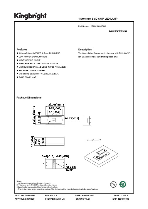
![ADG1608_1609[2]](https://img.taocdn.com/s1/m/52bc8720482fb4daa58d4bec.png)


XL-1608UGC-04Technical Data Sheet 0603翠绿haracteristics*外观尺寸(L/W/H):1.6*0.8*0.4mmQutline Dimensions(L/w/h):1.6*0.8*0.4mm*发光颜色及胶体:翠绿色/白色胶体Luminous color and colloid:Emerald green/white colloid*环保工艺符合ROHS要求Environmental protection products Complied With ROHS Directive*EIA规范标准包装EIA standard packaging*适用于SMT贴片自动化生产Suitable for SMT automatic production*适用于红外线回流焊制程Suitable for infrared reflow soldering processroduct application*医用设备:内窥镜、血氧仪Medical equipment:endoscope、oximeter*汽车电子:背光按键灯、指示灯Automotive electronics:backlight key light、indicator light*工业产品:电子仪表盘、工业设备Industrial products:electronic instrument panel、industrial equipment*智能家居:白色家电、数码管LEDSmart home:white appliances,nixie tube LED*通讯产品:手机按键灯、路由器、电视盒Communication products:mobile phone button lamp,routerCatalogueElectrical Characteristics (3)Typical Characteristic Curves (5)Reliability Test Items And Conditions (6)Outline Dimensions (7)Packaging (8)Guideline for Soldering (10)Precautions (12)1608UGC-04Electrical Characteristics(温度=25℃)Absolute Maximum Ratings (Temperature=25°C):Electro-Optical Charasteristics (Temperature=25°C):参数名称Parameter 符号Symbol 测试条件Test conditions最小值Min 典型值Typ 最大值Max 单位Unit 光强Light intensity IV IF=5mA 120-249mcd 正向电压Forward voltageVF 2.6 2.7 3.0V 主波长Dominant wavelengthλD 516-534nm 半光强视角Half light angle 2θ1/2-120-Deg 反向电流Reverse currentIRVR=5V --1μA参数名称Parameter 符号Symbol数值Rating 单位Unit消耗功率Consumed power Pd 80mW 正向脉冲电流Peak Forward currentIFP 100mA 正向工作电流Forward working currentI F 25mA 反向电压Reverse voltage V R 5V工作环境温度Operating ambient temperatureTopr -30℃~+85℃储存环境温度Storage ambient temperatureTstg -40℃~-90℃焊接条件Welding conditionsTsol回流焊(reflow soldering ):260°C ,10s 手动焊(manual welding ):300°C ,3s*注:脉冲宽度≤0.1ms ,占空比≤1/10*Note:Pulse width ≤0.1ms,Duty ≤1/10:Brightness gradingCodeMin Max Unit Test conditionsN2120144mcdIF=5mAN3144173N4173207N5207249:Voltage gradingCode Min Max Unit Test conditionsW10 2.6 2.7VIF=5mAW11 2.7 2.8W12 2.8 2.9W132.93.0:Wavelength gradingCode Min Max Unit Test conditionsG1516519nmIF=5mAG2519522G3522525G4525528G5528531G6531534Typical Characteristics Curves注:如无另外注明,测试环境温度为25+3︒C If not otherwise noted,the test ambient temperature is25+3︒C.可靠性实验Reliability experiment类别Class测试项目Test item测试环境Testing environment测试时间Testing time参考标准Reference standard耐久性测试Endurance test 工作寿命Working life室温条件下以最大额定电流持续点亮;以20mA测试(Continuous lighting at the maximum rated current at room temperature;Testit at 20mA.)1000小时1000hours (-24小时,+72小时)(-24hours ,+72hours MIL-STD-750D:1026MIL-STD-883D:1005JIS C 7021:B-1高温高湿储存High temperatureand highhumidityIR-Reflow In-Board,2Times环境温度Ta=85±5℃,相对湿度RH=90~95%240小时240hours (±2小时)(±2hours )MIL-STD-202F:103B JIS C 7021:B-11高温储存High -temperature storage 环境温度Ta=85±5℃1000小时1000hours (-24小时+72小时)(-24hours+72hours )MIL-STD-883D:1008JIS C 7021:B-10低温储存Low temperature storage环境温度Ta=-40±5℃JIS C 7021:B-12环境测试Environmentaltesting冷热循环Cold and hot cycle 105℃~25℃~-55℃~25℃30mins 5mins 30mins 5mins 50次循环50Circles MIL-STD-202F:107D MIL-STD-750D:1051MIL-STD-883D:1010冷热冲击Hot and cold impact IR-Reflow In-Board,2Times 100±5℃~-40℃±5℃20mins 20mins 50次循环50Circles MIL-STD-202F:107D MIL-STD-750D:1051MIL-STD-883D:1011抗锡试验Anti -tin test焊锡温度T.sol=260±5℃10±1secs 2次2timesMIL-STD-202F:210A MIL-STD-750D:2031JIS C 7021:A-1红外回流焊无铅制程InfraredreflowweldingThere is lead process 升温速度heat up speed (183℃到最高值):最大3℃/秒维持温度keep temperature 在125(±25)℃:不超过120秒维持温度keep temperature 在183℃以上:60-150秒最高温度限制范围maximum temperature :235℃+5/-0℃维持keep 在235℃+5/-0℃时间:10-15秒降温速度cooling rate :最大6℃/秒--------MIL-STD-750D:2031.2J-STD-020C红外回流焊无铅制程Infraredreflowwelding Lead-free process 升温速度heat up speed (217℃到最高值):最大3℃/秒维持温度keep temperature 在175(±25)℃:不超过180秒维持温度keep temperature 在217℃以上:60-120秒最高温度限制范围maximum temperature :255℃+0/-5℃维持keep 在255℃+0/-5℃时间:5-10秒降温速度cooling rate :最大6℃/秒--------MIL-STD-750D:2031.2J-STD-020C可焊性试验Weldabilitytest焊锡温度T.sol=235±5℃浸入速度:25±2.5mm/秒上锡率≧95%焊盘面积浸入时间:2±0.5秒MIL-STD-202F:208D MIL-STD-750D:2026MIL-STD-883D:2003IEC 68Part 2-20JIS C 7021:A-2Outline Dimension备注: 1.单位:毫米(mm)Remarks:1Unit:mm2.公差:如无特别标注则为±0.10mm2.Tolerance:±0.10mm unless otherwise specified1Packaging(1)Belt and disk dimensions注:1.尺寸单位为毫米(mm)。

Product data sheetCharacteristicsNSC160S3160NNSC160S TM160D 断路器 - 3P/3d主要信息产品系列Osmart NSC 产品类型断路器产品短名NSC160S Rated current 160 A 断路器应用配电保护极数3P额定电流 [In]160 A 在…上 40 °C分断能力25 KA Icu 在…上 220/240 V AC 50/60 Hz 符合 IEC 60947-2 18 KA Icu 在…上 380 V AC 50/60 Hz 符合 IEC 60947-2 18 KA Icu 在…上 400 V AC 50/60 Hz 符合 IEC 60947-2补充信息保护极说明3D 断路器型号S 电网类型AC 电网频率50/60 Hz 控制类型手柄安装类型固定式安装方式底板安装连接方式-上端前连接连接方式-下端前连接额定绝缘电压 [Ui]690 V 符合 IEC 60947-2额定冲击耐受电压 [Uimp]6 KV conforming to IEC 60947-2额定工作电压 [Ue]440 V AC 50/60 Hz 符合 IEC 60947-2使用类别AC类额定使用短路分断能力[Ics]50 % 在…上 380/400 V AC 50/60 Hz 符合 IEC 60947-2 50 % 在…上 220/240 V AC 50/60 Hz 符合 IEC 60947-2机械寿命10000 次电气寿命5000 次 符合 IEC 60947-2相间距35 Mm 脱扣器名称TM-D 脱扣器类型热磁式脱扣器额定值160 A 在…上 40 °C 保护类型短路保护 (磁保护) 过载保护 (热保护)长延时电流整定类型固定式长延时电流整定值 [Ir] 1 In 长延时时间整定类型固定式T h e i n f o r m a t i o n p r o v i d e d i n t h i s d o c u m e n t a t i o n c o n t a i n s g e n e r a l d e s c r i p t i o n s a n d /o r t e c h n i c a l c h a r a c t e r i s t i c s o f t h e p e r f o r m a n c e o f t h e p r o d u c t s c o n t a i n e d h e r e i n .T h i s d o c u m e n t a t i o n i s n o t i n t e n d e d a s a s u b s t i t u t e f o r a n d i s n o t t o b e u s e d f o r d e t e r m i n i n g s u i t a b i l i t y o r r e l i a b i l i t y o f t h e s e p r o d u c t s f o r s p e c i f i c u s e r a p p l i c a t i o n s .I t i s t h e d u t y o f a n y s u c h u s e r o r i n t e g r a t o r t o p e r f o r m t h e a p p r o p r i a t e a n d c o m p l e t e r i s k a n a l y s i s , e v a l u a t i o n a n d t e s t i n g o f t h e p r o d u c t s w i t h r e s p e c t t o t h e r e l e v a n t s p e c i f i c a p p l i c a t i o n o r u s e t h e r e o f .N e i t h e r S c h n e i d e r E l e c t r i c I n d u s t r i e s S A S n o r a n y o f i t s a f f i l i a t e s o r s u b s i d i a r i e s s h a l l b e r e s p o n s i b l e o r l i a b l e f o r m i s u s e o f t h e i n f o r m a t i o n c o n t a i n e d h e r e i n .瞬时保护电流整定类型固定式短路瞬时保护1600 KA高度165 Mm宽度105 Mm深度60 Mm净重 1.3 Kg环境符合标准IEC 60947-2产品认证CE污染等级 3 符合 IEC 60947运行温度-25…70 °C贮存环境温度-35…85 °C包装单位Unit Type of Package 1PCENumber of Units in Package 11Package 1 Height14.51 CmPackage 1 Width18.22 CmPackage 1 Length11.37 CmPackage 1 Weight 1.517 KgUnit Type of Package 2CARNumber of Units in Package 28Package 2 Height26 CmPackage 2 Width30.6 CmPackage 2 Length39.7 CmPackage 2 Weight12.73 KgUnit Type of Package 3PALNumber of Units in Package 3128Package 3 Height106 CmPackage 3 Width62 CmPackage 3 Length80.5 CmPackage 3 Weight220.8 Kg可持续性产品类型Green Premium 产品REACh法规REACh 声明REACh(不含 SVHC)是欧盟ROHS指令符合豁免条件无汞是RoHS 豁免信息是环境披露产品环境文件流通资料无需具体的回收操作循环配置文件合同保修保修单18 个月Product Life Status :Commercialised。

E M C C o m p o n e n t sJuly 2016片式磁珠电源线用MPZ系列MPZ1608型MPZ16081608[0603 inch]** 表示尺寸代码。
使用注意事项在使用本产品前,请务必随附采购规格书。
安全注意事项使用本产品时,请注意安全事项。
保存时间为12个月以内,保存条件(温度5~40°C 、湿度10~75%RH 以下),需充分注意。
若超过保存时间,端子电极的可焊性将可能老化。
请勿在气体腐蚀环境(盐、酸、碱等)下使用和保管。
在实施焊接前,请务必进行预热。
预热温度与焊接温度及芯片温度的温度差要在150°C 以内。
安装后的焊接修正应在规格书规定的条件范围内。
若加热过度可能导致短路、性能降低、寿命减少。
将安装了芯片的印刷电路组装到装置时,请注意不要因印刷电路整体变形或紧固部等局部变形而给芯片施加剩余应力。
装置会因通电而自我发热(温度上升),因此在热设计方面需留有充分余地。
非磁屏蔽型在基板设计时需注意配置线圈。
受到电磁干扰可能会导致误动作。
由于人体所带的静电会传到接地线上,因此请使用防静电腕带。
请勿将本产品靠近磁铁或带有磁力的物体。
请在采购规格书规定的范围内使用。
本产品目录中记载的产品是指在通用标准用途意义上使用于一般电子设备(AV 设备,通信设备,家电产品,娱乐设备,计算机设备,个人设备,办公设备,计测设备,工业机器人),并且该一般电子设备要在通常的操作和使用方法下使用。
对于需要高度安全性和可靠性的,或者设备的故障,误动作,运转不良可能会给人的生命,身体及财产等造成损害,以及有可能产生莫大社会影响的以下用途(以下称‘ 特定用途’)中的适用性,性能发挥,品质,本公司不予保证。
客户预定在本产品目录的范围,条件之外,或者在特定用途中使用时,请事先咨询本公司相关部门。
本公司会配合客户需求,一起协商不同于本产品目录中所记载的使用用途。
(1) 航空,航天设备(2) 运输设备(汽车,电车,船舶等)(3) 医疗设备(4) 发电控制设备(5) 核动力相关设备 (6) 海底设备(7) 交通工具控制设备(8) 公共性的高度信息处理设备(9) 军用设备(10) 电热用品,燃烧设备(11) 防灾防盗设备(12) 各种安全装置(13) 其他被认定为特定用途的用途此外,对使用本产品目录中所记载产品的设备进行设计时,请确保符合该设备的使用用途及状态的保护回路和装置,并设置备用回路等。

APT60DQ120SGDatasheet Ultrafast Soft Recovery Rectifier DiodeFinalApril 2018Contents1Revision History (1)1.1Revision A (1)2Product Overview (2)2.1Benefits (2)2.2Applications (2)3Electrical Specifications (3)3.1Absolute Maximum Ratings (3)3.2Electrical Performance (3)3.3Dynamic Characteristics (4)3.4Typical Performance Curves (4)3.5Reverse Recovery Overview (6)4Package Specification (7)4.1Package Outline Drawing (7)1Revision HistoryThe revision history describes the changes that were implemented in the document. The changes arelisted by revision, starting with the most current publication.1.1Revision ARevision A was published in April 2018. It is the first publication of this document.2Product OverviewFeaturesThe following are key features of the APT60DQ120SG device:Ultrafast recovery timesSoft recovery characteristicsLow forward voltageLow leakage currentAvalanche energy ratedRoHS compliant2.1BenefitsThe following are benefits of the APT60DQ120SG device:Higher switching frequencyLow switching lossesLow noise (EMI) switchingHigher reliability systemsIncreased system power density2.2ApplicationsThe APT60DQ120SG device is designed for the following applications: Power Factor Correction (PFC)Anti-parallel diodeSwitch-mode power supplyInverters/convertersMotor controllersFreewheeling diodeSwitch-mode power supplyInverters/convertersSnubber/clamp diode3Electrical SpecificationsThis section shows the electrical specifications for the APT60DQ120SG device.3.1Absolute Maximum RatingsThe following table shows the absolute maximum ratings for the APT60DQ120SG device.All ratings: T = 25 °C unless otherwise specified.CTable 1 • Absolute Maximum RatingsSymbol Parameter Ratings UnitV R Maximum DC reverse voltage1200VV RRM Maximum peak repetitive reverse voltage1200V RWM Maximum working peak reverse voltage1200I F(AV)Maximum average forward current (T = 103 °C, duty cycle = 0.5)C60AI F(RMS)RMS forward current87I FSM Non-repetitive forward surge current (T = 45 °C, 8.3 ms)J540E AVL Avalanche energy (1 A, 40 mH)20mJT , TJ STG Operating and storage temperature range–55 to 175°CT L Lead temperature for 10 seconds300The following table shows the thermal and mechanical characteristics of the APT60DQ120SG device.Table 2 • Thermal and Mechanical CharacteristicsSymbol Characteristic Min Typ Max UnitRθJC Junction-to-case thermal resistance0.40°C/WW T Package weight0.14oz4.0g 3.2Electrical PerformanceThe following table shows the static characteristics of the APT60DQ120SG device.Table 3 • Static CharacteristicsSymbol Characteristic Test Conditions Min Typ Max UnitV F Forward Voltage I = 60 AF 2.8 3.3VI = 120 AF 3.35I = 60 A, T = 125 °CF J 2.11I RM Maximum reverse leakage current V = 1200 VR100μAV = 1200 V, T = 125 °CR J500C J Junction capacitance V = 200 VR37pF3.3Dynamic CharacteristicsThe following table shows the dynamic characteristics of the APT60DQ120SG device.Table 4 • Dynamic CharacteristicsSymbol Characteristic Test ConditionsMin Typ Max Unit t rrReverse recovery timeI = 1 A, di /dt = –100 A/µs F F V = 30 V R T = 25 °CJ30nst rr Reverse recovery time I = 60 A, di /dt = –200 A/µs F F V = 800 V R T = 25 °CC 320 Q rr Reverse recovery change 630 nC I RRM Maximum reverse recovery current 5 A t rr Reverse recovery time I = 60 A, di /dt = –200 A/µs F F V = 800 V R T = 125 °CC 420 ns Q rr Reverse recovery charge 2810 nC I RRM Maximum reverse recovery current 12 A t rr Reverse recovery time I = 60 A, di /dt = –1000 A/µs F F V = 800 V R T = 125 °CC 190 ns Q rr Reverse recovery change 4415 nC I RRMMaximum reverse recovery current38A3.4Typical Performance CurvesThis section shows the typical performance curves for the APT60DQ120SG device.Figure 1 • Maximum Transient Thermal ImpedanceFigure 2 • Forward Current vs. Forward Voltage Figure 3 • trr vs. Current Rate of ChangeFigure 2 • Forward Current vs. Forward Voltage Figure 3 • trr vs. Current Rate of ChangeFigure 4 • Qrr vs. Current Rate of Change Figure 5 • IRRM vs. Current Rate of ChangeFigure 6 • Dynamic Parameters vs. Junction TemperatureFigure 7 • Maximum Average Forward Current vs. Case TemperatureFigure 8 • Junction Capacitance vs. Reverse Voltage1. 2. 3. 4. 5.Figure 8 • Junction Capacitance vs. Reverse Voltage3.5Reverse Recovery OverviewThe following illustration shows the reverse recovery testing and measurement information for the APT60DQ120SG device.Figure 9 • Diode Reverse Recovery Waveform and DefinitionsI —Forward conduction current.F di /dt—Rate of diode current change through zero crossing.F I —Maximum reverse recovery current.RRM t —Reverse recovery time, measured from zero crossing where diode current goes from positive to rr negative, to the point at which the straight line through I and 0.25 × I passes through zero.RRM RRM Q —Area under the curve defined by I and t .rr RRM rr4Package SpecificationThis section outlines the package specification for the APT60DQ120SG device.4.1Package Outline DrawingThis section details the D PAK package drawing of the APT60DQ120SG device. Dimensions are in3millimeters and (inches).Figure 10 • Package Outline DrawingMicrosemi Corporate HeadquartersOne Enterprise, Aliso Viejo,CA 92656 USAWithin the USA: +1 (800) 713-4113Outside the USA: +1 (949) 380-6100Fax: +1 (949) 215-4996Email:***************************© 2018 Microsemi Corporation. All rights reserved. Microsemi and the Microsemi logo are trademarks of Microsemi Corporation. All other trademarks and service marks are the property of their respective owners.Microsemi makes no warranty, representation, or guarantee regarding the information contained herein or the suitability of its products and services for any particular purpose, nor does Microsemi assume any liability whatsoever arising out of the application or use of any product or circuit. The products sold hereunder and any other products sold by Microsemi have been subject to limited testing and should not be used in conjunction with mission-critical equipment or applications. Any performance specifications are believed to be reliable but are not verified, and Buyer must conduct and complete all performance and other testing of the products, alone and together with, or installed in, any end-products. Buyer shall not rely on any data and performance specifications or parameters provided by Microsemi. It is the Buyer's responsibility to independently determine suitability of any products and to test and verify the same. The information provided by Microsemi hereunder is provided "as is, where is" and with all faults, and the entire risk associated with such information is entirely with the Buyer. Microsemi does not grant, explicitly or implicitly, to any party any patent rights, licenses, or any other IP rights, whether with regard to such information itself or anything described by such information. Information provided in this document is proprietary to Microsemi, and Microsemi reserves the right to make any changes to the information in this document or to any products and services at any time without notice.Microsemi Corporation (Nasdaq: MSCC) offers a comprehensive portfolio of semiconductor and system solutions for aerospace & defense, communications, data center and industrial markets. Products include high-performance and radiation-hardened analog mixed-signal integrated circuits, FPGAs, SoCs and ASICs; power management products; timing and synchronization devices and precise time solutions, setting the world's standard for time; voice processing devices; RF solutions; discrete components; enterprise storage and communication solutions; security technologies and scalable anti-tamper products; Ethernet solutions; Power-over-Ethernet ICs and midspans; as well as custom design capabilities and services. Microsemi is headquartered in Aliso Viejo, California, and has approximately 4,800 employees globally. Learn more at .053-4250。


QSLP1QF10.8mm Height Flat Top LEDFeatures• Package in 8mm tape on 7” diameter reel• Compatible with automatic placement equipment• Compatible with infrared and vapor phase reflow solder process • Mono-color type • RoHS complianceApplications• Automotive: Backlighting in dashboards and switch • Telecommunication: indicator and backlighting in telephone and fax• Flat backlight for LCD, switches and symbolsDescriptions• The SMD series enables smaller board size, higher packing density, reduced storage space, and small equipment• Besides, light weight makes them ideal for miniature applications • Applications include automotive, telecommunications and backlightingDevice Selection GuideChipPart No.MaterialEmitted Color Lens ColorTSP1-QF1608H8A4AlGaInPHyper RedWater ClearAbsolute Maximum Ratings (T a=25°C)Parameter Symbol Value Unit Reverse Voltage V F 5 V Forward Current I F 25 mA Peak Forward CurrentI FP100 mA(Duty 1/10 @1KHz)Power Dissipation P d60 mW Electrostatic Discharge ESD 2000 V Soldering Temperature T so 260 (for 5 seconds) °COperating Temperature T opr-40 ~ +85 °CStorage Temperature T stg-40 ~ +90 °CElectro-Optical Characteristics (T a=25°C)Parameter Symbol Min. Typ. Max. Unit Condition----- 5 ----- I F =2mAmcdLuminous Intensity I V45 76 -----Viewing Angle 2θ1/2 ----- 100 ----- degPeak Wavelength λp----- 632 ----- nmI F =20mADominant wavelength λd----- 624 ----- nmSpectrum Radiation Bandwidth △λ----- 20 ----- nmForward Voltage V F----- 2.0 2.4 VReverse Current I R----- ----- 10 µA V R=5VNotes:1. Tolerance of Luminous Intensity ±10%2. Tolerance of Dominant Wavelength ±1nm3. Tolerance of Forward Voltage ±0.05VSpectrum DistributionWavelength λp (nm ) Luminous Intensity vs. Forward CurrentForward Current I F (mA )Forward Current Derating CurveAmbient Temperature T a (°C )Forward Current vs. ForwardVoltageForward Voltage (V F )-voltsTypical Electro-Optical Characteristics CurvesLuminous Intensity vs. Ambient Temperature Ambient Temperature T a (°C ) F o r w a r d C u r r e n t I F (m A )Radiation Diagram (T a =25°C)R e l a t i v e l u m i n o u s i n t e n s i t y (%)R e l a t i v e l u m i n o u s i n t e n s i t y (%)F o r w a r d C u r r e n t I F (m A )R e l a t i v e l u m i n o u s i n t e n s i t y (%)Reliability Test Items and ConditionsThe reliability of products shall be satisfied with items listed below. Confidence level: 90%,LTPD: 10%No. Items Test Condition Test Hours /CyclesSampleSizeAc/Re1 Solder Heat Temp.: 260°C ±5°C. 5 Sec 76 PCS. 0/12 TemperatureCycle H: +85°C 30min∫ 5 minL: -55°C 15min50 Cycles 76PCS. 0/13 ThermalShock H: +100°C 5min∫ 10 secL: -10°C 5min50 Cycles 76PCS. 0/14 High Temperature Storage Temp: 100°C 1000 Hrs. 76 PCS. 0/15 Low Temperature Storage Temp: -40°C 1000 Hrs. 76 PCS. 0/16 DCOperatingLife I F = 20 mA 1000 Hrs. 76 PCS. 0/1 7 High Temperature / High Humidity 85°C / 85%RH 1000 Hrs. 76 PCS. 0/1Package Dimensions (In mm)Note: The tolerances unless mentioned is ±0.1mm, Unit = mm Carrier Tape Dimensions Loaded quantity 3000pcs per reel (In mm)Reel DimensionsNote: The tolerances unless mentioned is ±0.1mm, Unit = mm Test CircuitOrdering InformationTS P 1– Q F 1608 H8A4- 92-TR70How to contact us。