SiT8008数据手册-SiTime低功耗1-110MHz任意频率单端有源晶振
- 格式:pdf
- 大小:1.07 MB
- 文档页数:17

版本号:V20090929南京美尔诺电子版本所有目录第一章产品简介及特点 (4)第二章技术规格 (5)2.1 主要技术规格 (5)2.2 补充特性 (7)2.3 M88系列电源尺寸图 (7)第三章快速入门 (9)3.1前后面板描述 (9)3.2预先检查 (10)3.3 如果电源不能启动 (11)3.4 电源把手的调节方法 (11)3.5 电源上架安装 (12)第四章面板操作 (14)4.1键盘安排 (14)4.2 前面板操作介绍 (15)4.3 电压设定操作 (16)4.4 电流设定操作 (16)4.5 存取操作 (16)4.6 菜单操作 (17)4.6.1 菜单描述 (17)4.6.2菜单功能 (20)4.7输出开/关操作 (23)4.8远端测量功能 (23)4.9毫欧表功能 (24)4.10电压表功能 (24)第五章远端操作模式 (25)5.1 M131或M133通讯转换接口 (25)5.2 电源与PC间的通讯 (26)第六章SCPI通信协议 (29)6.1 SCPI命令概述 (29)6.2 常用相关命令描述 (29)6.2.1 基本命令(IEEE-488.2 公用命令集) (29)6.2.2 M8800所指定的命令 (29)6.2.3 量测命令 (31)6.2.4设置命令 (32)6.2.5 顺序操作(List)相关命令 (34)第一章产品简介及特点M88系列电源是在普通实验室可编程电源基础上拔高设计的新一代产品。
本系列产品配备通讯接口,具有超快上升沿速度(M8811电源的上升速度可小于10mS,M8851电源的上升速度可小于20mS)。
M88系列电源兼具桌上型和系统型的特性,可任意搭配其他仪器,集成为特殊功能的测试系统,以完成不同场合下的测量需求。
可通过面板键盘编辑程序,兼具电压表,欧姆表的功能,给用户的使用带来极大的方便,是普通可编程电源的换代产品,具有极高的性价比优势。
本电源具有以下特点:•低纹波和低噪音•超高分辨率及精度0.1mV/0.01mA•内置高精度五位半电压表和毫欧姆表•支持高精度和动态编程输出•高亮度、真空VFD显示屏,双排四路同时显示•根据温度变化,无极伺服,智能风扇系统•支持远端电压补偿,多数据存储•支持外部触发输入、输出•开机自检,软件校正,标准仪器架设计•使用标准SCPI通信协议•支持TTL电平的串行口通讯第二章技术规格2.1 主要技术规格M881X系列电源技术规格表M885X系列电源的技术规格表2.2 补充特性状态存储器容量:50组操作状态建议校准频率:1次/年交流电源输入等级(可以通过电源后面板上的切换开关进行选择)Option Opt.01: 220VAC ±10%, 47 to 63 HzOption Opt.02: 110 VAC ±10%, 47 to 63 Hz散热方式:强制风冷操作环境温度:0 to 40 °C储存环境温度:-20 to 70 °C.使用环境:室内使用设计,污染等级2级,最大湿度95%2.3 M88系列电源尺寸图M881X和M8831系列的尺寸为214mmW x 108mmH x 365mmD,请参看下列尺寸图:图2.1 M881X电源尺寸图M885X系列的尺寸为428mmW×103.5mmH×453.5mmD,请参看以下尺寸图:图2.2 M885X电源尺寸图第三章快速入门本章将简单介绍M88系列电源的外观及基本功能,让您快速认识M88系列电源。

SiT8008BLow Power Programmable OscillatorFeatures⏹Any frequency between 1 MHz and 110 MHz accurate to6 decimal places⏹100% pin-to-pin drop-in replacement to quartz-based XO⏹Excellent total frequency stability as low as ±20 ppm⏹Operating temperature from -40°C to 85°C. For 125°C and/or-55°C options, refer to SiT1618, SiT8918, SiT8920⏹Low power consumption of 3.5 mA typical at 1.8V⏹Standby mode for longer battery life⏹Fast startup time of 5 ms⏹LVCMOS/HCMOS compatible output⏹Industry-standard packages: 2.0 x 1.6, 2.5 x 2.0, 3.2 x 2.5,5.0 x 3.2, 7.0 x 5.0 mm x mm⏹Instant samples with Time Machine II and field programmableoscillators⏹RoHS and REACH compliant, Pb-free, Halogen-free andAntimony-free⏹For AEC-Q100 oscillators, refer to SiT8924 and SiT8925Applications⏹Ideal for DSC, DVC, DVR, IP CAM, Tablets, e-Books,SSD, GPON, EPON, etc⏹Ideal for high-speed serial protocols such as: USB,SATA, SAS, Firewire, 100M / 1G / 10G Ethernet, etc.Electrical CharacteristicsAll Min and Max limits are specified over temperature and rated operating voltage with 15 pF output load unless otherwise stated. Typical values are at 25°C and nominal supply voltage.Table 1. Electrical CharacteristicsSiT8008B Low Power Programmable OscillatorTable 1. Electrical Characteristics (continued)Table 2. Pin DescriptionTop ViewFigure 1. Pin Assignments1. In OE or ST mode, a pull-up resistor of 10 kΩ or less is recommended if pin 1 is not externally driven. If pin 1 needs to be left floating, use the NC option.2. A capacitor of value 0.1 µF or higher between Vdd and GND is required.1423OE/ST/NCGNDOUTVDDTable 3. Absolute Maximum LimitsAttempted operation outside the absolute maximum ratings may cause permanent damage to the part. Actual performance of the IC is only guaranteed within the operational specifications, not at absolute maximum ratings.Note:3. Exceeding this temperature for extended period of time may damage the device.Table 4. Thermal Consideration[4]Note:4. Refer to JESD51 for θJA and θJC definitions, and reference layout used to determine the θJA and θJC values in the above table.Table 5. Maximum Operating Junction Temperature[5]Note:5. Datasheet specifications are not guaranteed if junction temperature exceeds the maximum operating junction temperature.Table 6. Environmental ComplianceHZHZHZTest Circuit and Waveform [6]VddVoutTestPointtr80% Vdd50% 20% VddNote:Figure 2. Test CircuitFigure 3. Waveform6. Duty Cycle is computed as Duty Cycle = T H/Period.Timing DiagramsPin 4T_start: Time to start from power-off T_resume: Time to resume from STFigure 4. Startup Timing (OE/ST Mode)Figure 5. Standby Resume Timing (ST Mode O nly)CLK OutputT_oe: Time to re-enable the clock outputT_oe: Time to put the output in High Z m odeFigure 6. OE Enable Timing (OE Mode Only)Figure 7. OE Disable Timing (OE Mode Only)Note:7. SiT8008 has “no runt” pulses and “no glitch” output during startup or resume.HZtfHigh Pulse (TH)Low Pulse (TL)Period5.5 5.0 4.5 4.03.5 010 20 30 40 50 60 70 80 90 100 110Frequency (MHz) -40 -30 -20 -10 010 20 3040 50 60 70 80Temperature (°C)Figure 8. Idd vs FrequencyFigure 9. Frequency vs T emperatureFigure 10. RMS Period Jitter vs FrequencyFigure 11. Duty Cycle vs FrequencyFigure 12. 20%-80% Rise Time vs TemperatureFigure 13. 20%-80% Fall Time vs T emperatureFigure 14. RMS Integrated Phase Jitter Random(12 kHz to 20 MHz) vs Frequency [9]Figure 15. RMS Integrated Phase Jitter Random(900 kHz to 20 MHz) vs Frequency [9]Notes:8. All plots are measured with 15 pF load at room temperature, unless otherwise stated.9. Phase noise plots are measured with Agilent E5052B signal source analyzer. Integration range is up to 5 MHz for carrier frequencies below 40 MHz.10305070 90 110Frequency (MHz)Programmable Drive StrengthThe SiT8008 includes a programmable drive strength feature to provide a simple, flexible tool to optimize the clock rise/fall time for specific applications. Benefits from the programmable drive strength feature are:⏹Improves system radiated electromagnetic interfer-ence (EMI) by slowing down the clock rise/fall time. ⏹Improves the downstream clock receiver’s (RX) jitterby decreasing (speeding up) the clock rise/fall time. ⏹Ability to drive large capacitive loads while maintainingfull swing with sharp edge rates.For more detailed information about rise/fall time control and drive strength selection, see the SiTime Application Notes section: /support/application-notes.EMI Reduction by Slowing Rise/Fall TimeFigure 16 shows the harmonic power reduction as the rise/fall times are increased (slowed down). The rise/fall times are expressed as a ratio of the clock period. For the ratio of 0.05, the signal is very close to a square wave. For the ratio of 0.45, the rise/fall times are very close to near-triangular waveform. These results, for example, show that the 11th clock harmonic can be reduced by 35 dB if the rise/fall edge is increased from 5% of the period to 45% of the period.Jitter Reduction with Faster Rise/Fall TimePower supply noise can be a source of jitter for the down-stream chipset. One way to reduce this jitter is to speed up the rise/fall time of the input clock. Some chipsets may also require faster rise/fall time in order to reduce their sensitivity to this type of jitter. Refer to the Rise/Fall Time Tables (Table 7 to Table 11) to determine the proper drive strength.High Output Load CapabilityThe rise/fall time of the input clock varies as a function of the actual capacitive load the clock drives. At any given drive strength, the rise/fall time becomes slower as the output load increases. As an example, for a 3.3V SiT8008 device with default drive strength setting, the typical rise/fall time is 1 ns for 15 pF output load. The typical rise/fall time slows down to 2.6 ns when the output load increases to 45 pF. One can choose to speed up the rise/fall time to 1.83 ns by then increasing the drive strength setting on the SiT8008. The SiT8008 can support up to 60 pF or higher in maxi-mum capacitive loads with drive strength settings. Refer to the Rise/Fall Time Tables (Table 7 to 11) to determine the proper drive strength for the desired combination of output load vs. rise/fall time.SiT8008 Drive Strength SelectionTables 7 through 11define the rise/fall time for a given capacitive load and supply voltage.1. Select the table that matches the SiT8008 nominalsupply voltage (1.8V, 2.5V, 2.8V, 3.0V, 3.3V).2. Select the capacitive load column that matches theapplication requirement (5 pF to 60 pF)3. Under the capacitive load column, select the desiredrise/fall times.4. The left-most column represents the part numbercode for the corresponding drive strength.5. Add the drive strength code to the part number forordering purposes.Calculating Maximum FrequencyAny given rise/fall time in Table 7 through 11dictates the maximum frequency under which the oscillator can operate with guaranteed full output swing over the entire operating temperature range. This max frequency can be calculated as the following:=15 x Trf_20/80Max Frequencywhere Trf_20/80 is the typical value for 20%-80% rise/fall time.Example 1Calculate f MAX for the following condition:⏹Vdd = 1.8V (Table 7)⏹Capacitive Load: 30 pF⏹Desired Tr/f time = 3 ns (rise/fall time part numbercode = E)⏹f MAX = 66.666660Part number for the above example:SiT8008I E12-18E-66.666660Drive strength code is inserted here. Def ault setting is “-”Figure 16. Harmonic EMI reduction as a Function of Slower Rise/Fall TimeRise/Fall Time (20% to 80%) vs C LOAD TablesTable 7. Vdd = 1.8V Rise/Fall Times for Specific C LOAD Table 8. Vdd = 2.5V Rise/Fall Times for Specific C LOADTable 9. Vdd = 2.8V Rise/Fall Timesfor Specific C LOADTable 10. Vdd = 3.0V Rise/Fall Timesfor Specific C L OA DTable 11. Vdd = 3.3V Rise/Fall Timesfor Specific C LOA DPin 1 Configuration Options (OE, ST, or NC) Pin 1 of the SiT8008 can be factory-programmed to support three modes: Output Enable (OE), standby (ST) or No Con-nect (NC). These modes can also be programmed with the Time Machine using field programmable devices.Output Enable (OE) ModeIn the OE mode, applying logic Low to the OE pin only disables the output driver and puts it in Hi-Z mode. The core of the device continues to operate normally. Power consumption is reduced due to the inactivity of the output. When the OE pin is pulled High, the output is typically en-abled in <1 µs.Standby (ST) ModeIn the ST mode, a device enters into the standby mode when Pin 1 pulled Low. All internal circuits of the device are turned off. The current is reduced to a standby current, typi-cally in the range of a few µA. When ST is pulled High, the device goes through the “resume” process, which can take up to 5 ms.No Connect (NC) ModeIn the NC mode, the device always operates in its normal mode and outputs the specified frequency regardless of the logic level on pin 1.Table 12 below summarizes the key relevant parameters in the operation of the device in OE, ST, or NC mode.Table 12. OE vs. ST vs. NCOutput on Startup and ResumeThe SiT8008 comes with gated output. Its clock output is ac-curate to the rated frequency stability within the first pulse from initial device startup or resume from the standby mode. In addition, the SiT8008 features “no runt” pulses and “no glitch”output during startup or resume as shown in the waveform captures in Figure 17 and Figure 18.Figure 18. Startup Waveform vs. Vdd(Zoomed-in View of Figure 17)Instant Samples with Time Machine and Field Programmable OscillatorsSiTime supports a field programmable version of the SiT8008 low power oscillator for fast prototyping and real time custom- ization of features. The field programmable devices(FP devices) are available for all five standard SiT8008 package sizes and can be configured to one’s exact specification using the Time Machine II, an USB powered MEMS oscillator programmer.Customizable Features of the SiT8008 FP Devices Include⏹Frequency between 1 MHz to 110 MHz⏹Three frequency stability options, ±20 ppm, ±25ppm, ±50 ppm⏹Two operating temperatures, -20 to 70°C or -40 to 85°C⏹Six supply voltage options, 1.8V, 2.5V, 2.8V, 3.0V,3.3V and⏹ 2.25 to 3.63V continuous⏹Output drive strength⏹OE, ST or NC modeFor more information regarding SiTime’s field programm a-ble solutions, visit /time-machine and /fp-devices.SiT8008 is typically factory-programmed per customer ordering codes for volume delivery.Figure 17. Startup Waveform vs. VddDimensions and PatternsDimensions and PatternsNotes:10. Top marking: Y denotes manufacturing origin and XXXX denotes manufacturing lot number. The value of “Y” will depend on the as sembly location of thedevice.11. A capacitor of value 0.1 µF or higher between Vdd and GND is required.Ordering InformationThe Part No. Guide is for reference only. To customize and build an exact part number, use the SiTime Part Number Generator.Table 13. Ordering Codes for Supported Tape & Reel Packing MethodPacking Method“D”: 8 mm Tape & Reel, 3ku r eel “E”: 8 mm Tape & Reel, 1ku reel “T”: 12/16 mm Tape & Reel, 3ku reel “Y”: 12/16 mm Tape & Reel, 1ku reel Blank for BulkFrequency1.000000 to 110.000000 MHz Feature Pin“E” for Output Enable “S” for Standby “N” for No Connect Supply Voltage“18” for 1.8V ±10% “25” for 2.5V ±10% “28” for 2.8V ±10% “30” for 3.0V ±10% “33” for 3.3V ±10%“XX” for 2.5V -10% to 3.3V +10% Part Family “SiT8008” Revision Letter “B” is the revisionTemperature Range“C” Commerci al, -20ºC to 70ºC “I” Industrial, -40ºC to 85ºC Output Drive Strength “–” Default (datasheet limits) See Tables 7 to 11 for rise/fall times “L” “T” “A” “E” “R” “U” “B” “F” Package Size “7” 2.0 x 1.6 mm “1” 2.5 x 2.0 mm “2” 3.2 x 2.5 mm “3” 5.0 x 3.2 mm “8” 7.0 x 5.0 mmFrequency Stability “1” for ±20 ppm “2” for ±25 ppm “3” for ±50 ppmSiT8008BC-12-18E-66.666660DTable 14. Additional InformationTable 15. Revision HistorySiTime Corporation, 5451 Patrick Henry Drive, Santa Clara, CA 95054, USA | Phone: +1-408-328-4400 | Fax: +1-408-328-4439© SiTime Corporation 2014-2017. The information contained herein is subject to change at any time without notice. SiTime assumes no responsibility or l iability for any loss, damage or defect of a Product which is caused in whole or in part by (i) use of any circuitry other than circuitry embodied in a SiTime product, (ii) misuse or abuse including static discharge, neglect or accident, (iii) unauthorized modification or repairs which have been soldered or altered during assembly and are not capable of being tested by SiTime under its normal test conditions, or (iv) improper installation, storage, handling, warehousing or transportation, or (v) being subjected to unusual physical, thermal, or electrical stress.Disclaimer: SiTime makes no warranty of any kind, express or implied, with regard to this material, and specifically disclaims any and all express or implied warranties, either in fact or by operation of law, statutory or otherwise, including the implied warranties of merchantability and fitness for use or a particular purpose, and any implied warranty arising from course of dealing or usage of trade, as well as any common-law duties relating to accuracy or lack of negligence, with respect to this material, any SiTime product and any product documentation. Products sold by SiTime are not suitable or intended to be used in a life support application or component, to operate nuclear facilities, or in other mission critical applications where human life may be involved or at stake. All sales are made conditioned upon compliance with the critical uses policy set forth below.CRITICAL USE EXCLUSION POLICYBUYER AGREES NOT TO USE SITIME'S PRODUCTS FOR ANY APPLICATION OR IN ANY COMPONENTS USED IN LIFE SUPPORT DEVICES OR TO OPERATE NUCLEAR FACILITIES OR FOR USE IN OTHER MISSION-CRITICAL APPLICATIONS OR COMPONENTS WHERE HUMAN LIFE OR PROPERTY MAY BE AT STAKE.SiTime owns all rights, title and interest to the intellectual property related to SiTime's products, including any software, firmware, copyright, patent, or trademark. The sale of SiTime products doesSupplemental InformationBest ReliabilitySilicon is inherently more reliable than quartz. Unlike quartz suppliers, SiTime has in-house MEMS and analog CMOS expertise, which allows SiTime to develop the most reliable products. Figure 1 shows a comparison with quartz technology.Why is EpiSeal™ MEMS Best in Class:⏹SiTime’s MEMS resonators are vacuum sealed usingan advanced EpiSeal™ process, which eliminates foreign particles and improves long term aging andreliability⏹World-class MEMS and CMOS design expertise38Figure 1. Reliability Comparison[1]Best AgingUnlike quartz, MEMS oscillators have excellent long term aging performance which is why every new SiTime product specifies 10-year aging. A comparison is shown in Figure 2.Why is EpiSeal MEMS Best in Class:⏹SiTime’s MEMS resonators are vacuum sealed usingan advanced EpiSeal™ process, which eliminates foreign particles and improves long term aging and reliability⏹Inherently better immunity of electrostatically drivenMEMS resonatorFigure 2. Aging Comparison[2]Best Electro Magnetic Susceptibility (EMS)SiTime’s oscillators in plastic packages are up to 54 times more immune to external electromagnetic fields than quartz oscillators as shown in Figure 3.Why is EpiSeal MEMS Best in Class:⏹Internal differential architecture for best commonmode noise rejection⏹Electrostatically drivenMEMS resonator is more immune to EMSFigure 3. Electro Magnetic Susceptibility (EMS)[3] Best Power Supply Noise RejectionSiTime’s MEMS oscillators are more resilient against noise on the power supply. A comparison is shown in Figure 4. Why is EpiSeal MEMS Best in Class:⏹On-chip regulators and internal differential architecturefor common mode noise rejection⏹MEMS resonator is paired with advanced analogCMOS ICFigure 4. Power Supply Noise Rejection[4]Best Vibration RobustnessHigh-vibration environments are all around us. All electronics, from handheld devices to enterprise servers and storage systems are subject to vibration. Figure 5 shows a comparison of vibration robustness.Why is EpiSeal MEMS Best in Class:⏹The moving mass of SiTime’s MEMS resonators is up to 3000 times smaller than quartz⏹ Center-anchored MEMS resonator is the most robustdesignFigure 5. Vibration Robustness [5]Best Shock RobustnessSiTime’s oscillators can withstand at least 50,000 g shock. They all maintain their electrical performance in operation during shock events. A comparison with quartz devices is shown in Figure 6.Why is EpiSeal MEMS Best in Class:⏹The moving ma ss of SiTime’s MEMS resonators is up to 3000 times smaller than quartz⏹Center-anchored MEMS resonator is the most robustdesignFigure 6. Shock Robustness [6]Figure labels: ▪ TXC = TXC ▪ Epson = EPSN▪ Connor Winfield = CW ▪ Kyocera = KYCA ▪ SiLabs = SLAB▪SiTime = EpiSeal MEMSNotes:1. Data source: Reliability documents of named companies.2. Data source: SiTime and quartz oscillator devices datasheets.3. Test conditions for Electro Magnetic Susceptibility (EMS):▪According to IEC EN61000-4.3 (Electromagnetic compatibility standard)▪Field strength: 3V/m▪Radiated signal modulation: AM 1 kHz at 80% depth▪Carrier frequency scan: 80 MHz – 1 GHz in 1% steps▪Antenna polarization: Vertical▪DUT position: Center aligned to antennaDevices used in this test:4. 50 mV pk-pk Sinusoidal voltage.Devices used in this test:5. Devices used in this test:same as EMS test stated in Note 3.6. Test conditions for shock test:▪MIL-STD-883F Method 2002▪Condition A: half sine wave shock pulse, 500-g, 1ms▪Continuous frequency measurement in 100 μs gate time for 10 secondsDevices used in this test:same as EMS test stated in Note 3.7. Additional data, including setup and detailed results, is available upon request to qualified customer. Please contact *************************.Mouser ElectronicsAuthorized DistributorClick to View Pricing, Inventory, Delivery & Lifecycle Information:S iTime:SiT8008BI-82-25E-40.00000X SIT8008BI-12-25E-80.000000G SIT8008BI-12-33E-62.500000G SIT8008BI-73-33E-31.250000G SIT8008BI-12-25E-25.000000G SiT8008BC-81-33E-4.718592X SiT8008BI-13-18E-24.000000GSiT8008BI-23-33E-16.000000G SiT8008BC-11-33S-13.91222G SiT8008BC-11-33S-14.64000G SiT8008BC-33-18E-33.333330X SiT8008BI-73-33E-80.000000G SIT8008BI-31-33E-6.000000G SIT8008BI-31-33E-80.000000XSiT8008BI-32-18E-98.304000X SIT8008BI-33-33S-90.000000X SIT8008BI-73-25E-33.333330G SiT8008BI-73-33E-20.000000G SIT8008BI-31-33E-050.211000X SIT8008BI-31-33E-059.407060X SIT8008BI-31-33E-100.000000XSIT8008BI-31-33E-12.000000G SIT8008BI-31-33E-27.299640X SIT8008BI-31-33E-59.497670X SIT8008BI-12-18S-12.00000G SIT8008BI-12-18S-2.048000G SiT8008BI-13-33E-16.000000G SiT8008BI-13-33E-3.6864000GSiT8008BI-21-18S-70.00000G SiT8008BI-22-33E-24.000000G SiT8008BC-33-33E-4.718592X SiT8008BC-71-18E-10.000000G SIT8008BI-11-18E-33.333333G SIT8008BI-11-25E-66.000000G SIT8008BI-12-18E-20.7500GSIT8008BI-12-18E24.54545G SiT8008BI-33-18E-100.000000Y SiT8008BC-23-25E-32.000000G SiT8008BI-12-33E-65.000000E SiT8008BIL11-33S-24.806000E SiT8008BC-12-33S-8.000000E SiT8008BC-82-33E24.998125XSiT8008BC-12-33S-8.000000G SiT8008BC-82-33E24.998125Y SiT8008BI-21-33E-45.000000G SiT8008BI-21-33E-45.000000E SIT8008BC-83-33E-2.457600Y SIT8008BI-12-33E-65.000000G SiT8008BI-11-33E-47.388500ESiT8008BI-33-33E-16.000000Y SiT8008BI-33-33E-16.000000X SiT8008BIR23-XXS-100.000000E SiT8008BIR23-XXS-100.000000G SiT8008BI-31-XXS-10.00000X SiT8008BI-33-18E-100.000000X SIT8008BC-83-33E-2.457600X SiT8008BC-23-25E-32.000000E SIT8008BIL11-33S-24.806000G SiT8008BI-11-33E-47.388500G SiT8008BI-31-XXS-10.00000Y SiT8008BI-83-33E-25.000000Y SiT8008BI-12-XXE-1.843200E SiT8008BI-12-18E-11.289600ESiT8008BI-12-XXE-8.000000E SIT8008BI-83-33E-66.666000Y SiT8008BI-32-33E-8.000000Y SiT8008BI-12-18E-1.843200E SiT8008BI-82-33E-100.000000Y SiT8008BI-12-18E-8.000000E SiT8008BI-12-33E-11.289600ESiT8008BI-82-33E-16.000000Y SiT8008BI-12-25E-11.289600E SiT8008BC-82-33E-3.686400Y SiT8008BC-82-33E-12.288000Y SiT8008BI-32-33E-12.288000Y SiT8008BI-22-33E-2.048000E SiT8008BI-13-XXS-25.000000GSiT8008BC-12-33S-18.100000G SiT8008BC-23-33E-90.000000G SiT8008BC-12-33E-24.000000G SiT8008BI-11-18E-28.636363E。


Applications Note: AN_SY8009High Efficiency 1.5MHz/1MHz, 1.5A/2A Synchronous Step Down Regulator Preliminary Spec General DescriptionThe SY8009A and SY8009B are high-efficiency , high frequency synchronous step-down DC-DC regulator ICs capable of delivering up to 1.5A/2A output currents. The SY8009 family operate over a wide input voltage range from 3V to 5.5V and integrate main switch and synchronous switch with very low RDS(ON) to minimize the conduction loss. Low output voltage ripple and small external inductor and capacitor sizes are achieved with greater than 1MHz switching frequency.Features• low Rds(on) for internal switches (top/bottom) SY8009A: 200mohm/150mohm, 1.5A, SOT23-5 SY8009B:150mohm/120mohm,2.0A, SSOT23-6 • 3-5.5V input voltage range • High switching frequency minimizes the external components SY8009A: 1.5MHz SY8009B: 1MHz • Internal softstart limits the inrush current • 100% dropout operation • Compact package: SOT23-5 and Super SOT23-6 are pin-compatible. Other packages are available upon requestsOrdering InformationSY8009□(□□ □ □ □□ □□)□ Temperature Code C: - 40°C~85°C Package Code: AA:SOT23-5 EB:SSOT23-6 Spec CodeApplications• • • • •LCD TV Set Top Box Net PC Mini-Notebook PC Access Point RouterTypical ApplicationsVININ EN LXL C1(opt.) R1VOUTCINFB GNDCOUT R2Figure 1Efficiency (%)Figure2Efficiency vs Load CurrentAN_SY8009 Rev. 0.2Silergy Corp. Confidential- Prepared for Customer Use Only1AN_SY8009Pinout (top view)(SY8009A, SOT23-5)(SY8009B, SSOT23-6)Top Mark: ADxyz for SY8009A , ASxyz for SY8009B (Device code: AD for SY8009A and AS for SY8009B, x=year code, y=week code, z= lot number code) Pin Name EN GND LX IN FB Pin Number 1 2 3 4 6(SSOT23-6) Pin Description Enable control. Pull high to turn on. Do not float. Ground pin Inductor pin. Connect this pin to the switching node of inductor. Input pin. Decouple this pin to GND pin with at least 1uF ceramic cap. Output Feedback Pin. Connect this pin to the center point of the output resistor divider (as shown in Figure 1) to program the output voltage: Vout=0.6*(1+R1/R2).Absolute Maximum Ratings (Note 1)Supply Input Voltage ------------------------------------------------------------------------------------------ 6.0V Enable, FB Voltage--------------------------------------------------------------------------------------------- VIN + 0.6V Power Dissipation, PD @ TA = 25°C ,SOT23-5,SSOT23-6 --------------------------------------------- 0.4W Package Thermal Resistance (Note 2) SOT23-5,SSOT23-6, θ JA --------------------------------------------------------------------------- 250°C/W SOT23-5,SSOT23-6, θ JC ----------------------------------------------------------------------------130°C/W Junction Temperature Range ----------------------------------------- -----------------------------------------150°C Lead Temperature (Soldering, 10 sec.) ---------------------------------------------------------------------- 260°C Storage Temperature Range ---------------------------------------------------------------------------------- -65°C to 150°C ESD Susceptibility (Note 2) HBM (Human Body Mode) ----------------------------------------------------------------------------------- 2kV MM (Machine Mode) ------------------------------------------------------------------------------------------ 200VRecommended Operating Conditions (Note 3)Supply Input Voltage ------------------------------------------------------------------------------------------3V to 5.5V Junction Temperature Range -------------------------------------------------------------------------------- -40°C to 125°C Ambient Temperature Range -------------------------------------------------------------------------------- -40°C to 85°CAN_SY8009 Rev. 0.2Silergy Corp. Confidential- Prepared for Customer Use Only2AN_SY8009Electrical Characteristics(VIN = 5V, VOUT = 2.5V, L = 2.2uH, COUT = 10uF, TA = 25°C, unless otherwise specified)Parameter Input Voltage Range Quiescent Current Shutdown Current Feedback Reference Voltage FB Input Current PFET RON NFET RON PFET Current Limit EN rising threshold EN falling threshold Input UVLO threshold UVLO hysteresis Oscillator Frequency Min ON Time Max Duty Cycle Thermal Shutdown TemperatureSymbol VIN IQ ISHDN VREF IFB RDS(ON),P RDS(ON),N ILIM VENH VENL VUVLO VHYS FOSCTest Conditions IOUT=0, VFB=VREF ⋅ 105% EN=0Min 3Typ 80 0.1 0.6Max 5.5 1 0.612 500.588 VFB=VIN SY8009A SY8009B SY8009A SY8009B SY8009A SY8009B -50Unit V µA µA V nA Ω Ω Ω Ω A A V V V V MHz MHz ns % °C0.2 0.15 0.15 0.12 1.8 2.5 1.5 0.4 1.8 0.1 1.5 1 50 100 160IOUT=200mA, SY8009A IOUT=500mA, SY8009BTSDNote 1: Stresses listed as the above “Absolute Maximum Ratings” may cause permanent damage to the device. These are for stress ratings. Functional operation of the device at these or any other conditions beyond those indicated in the operational sections of the specifications is not implied. Exposure to absolute maximum rating conditions for extended periods may remain possibility to affect device reliability. Note 2: θ JA is measured in the natural convection at TA = 25°C on a low effective single layer thermal conductivity test board of JEDEC 51-3 thermal measurement standard. Pin 2 of SOT23-5/SSOT-23-5 packages is the case position for θ JC measurement. Note 3: The device is not guaranteed to function outside its operating conditions.AN_SY8009 Rev. 0.2Silergy Corp. Confidential- Prepared for Customer Use Only3AN_SY8009Typical Performance Characteristics(SY8009B)Efficiency vs Load Current Efficiency vs Load Current Efficiency vs Load CurrentOutput Ripple(Vin=5.0V, Vout=1.8V,Iload=0.5A)Output Ripple(Vin=5.0V, Vout=1.8V,Iload=1.5A)Output Ripple(Vin=5.0V, Vout=1.8V,Iload=2A)Startup(Vin=5.0V, Vout=1.8V,Iload=2A)Shutdown(Vin=5.0V, Vout=1.8V,Iload=2A)Short Protection/Current limit(Vin=5.0V, Vout=1.8V,open to short)AN_SY8009 Rev. 0.2Silergy Corp. Confidential- Prepared for Customer Use Only4AN_SY8009Soft Start(Vo) Soft Start(Lx) Load Transient(Vin=5.0VmVout=1.8V,Iload=0~1A)Load Transient(Vin=5.0V, Vout=1.8V,Iload=0.2~2A)Case Temperature vs Output Current Oscillator Frequency vs Vin(Vin=5V,Vo=1.8V,Ta=27℃)AN_SY8009 Rev. 0.2Silergy Corp. Confidential- Prepared for Customer Use OnlyTC(°C)5AN_SY8009OperationSY8009 is a synchronous buck regulator IC that integrates the PWM control, top and bottom switches on the same die to minimize the switching transition loss and conduction loss. With ultra low Rds(on) power switches and proprietary PWM control, this regulator IC can achieve the highest efficiency and the highest switch frequency simultaneously to minimize the external inductor and capacitor size, and thus achieving the minimum solution footprint.Applications InformationBecause of the high integration in the SY8009 IC, the application circuit based on this regulator IC is rather simple. Only input capacitor CIN, output capaictor COUT, output inductor L and feedback resistors (R1 and R2) need to be selected for the targeted applications specifications. Feedback resistor dividers R1 and R2: Choose R1 and R2 to program the proper output voltage. To minimize the power consumption under light loads, it is desirable to choose large resistance values for both R1 and R2. A value of between 10k and 200k is highly recommended for R2. If R2=100k is chosen, then R1 can be calculated to be:R1 =(VOUT − 0.6 V) ⋅ R2 0.6VInput capacitor CIN:With the maximum load current at 1.2A, the maximum ripple current through input capacitor is about 0.6Arms. A typical X7R or better grade ceramic capacitor with 6V rating and greater than 4.7uF capacitance can handle this ripple current well. To minimize the potential noise problem, place this ceramic capacitor really close to the IN and GND pins. Care should be taken to minimize the loop area formed by CIN, and IN/GND pins. Output capacitor COUT: The output capacitor is selected to handle the output ripple noise requirements. Both steady state ripple and transient requirements must be taken into consideration when selecting this capacitor. For the best performance, it is recommended to use X7R or better grade ceramic capacitor with 6V rating and greater than 4.7uF capacitance. Output inductor L: There are several considerations in choosing this inductor. 1) Choose the inductance to provide the desired ripple current. It is suggested to choose the ripple current to be about 40% of the maximum output current. The inductance is calculated as: VOUT (1 − VOUT/VIN,MAX ) L= FSW × IOUT,MAX × 40% where Fsw is the switching frequency and IOUT,MAX is the maximum load current. The SY8009 regulator IC is quite tolerant of different ripple current amplitude. Consequently, the final choice of inductance can be slightly off the calculation value without significantly impacting the performance. 2) The saturation current rating of the inductor must be selected to be greater than the peak inductor current under full load conditions. VOUT(1-VOUT/VIN,MAX) ISAT, MIN > IOUT, MAX + 2 ⋅ FSW ⋅ L 3) The DCR of the inductor and the core loss at the switching frequency must be low enough to achieve the desired efficiency requirement. It is desirable to choose an inductor with DCR<50mohm to achieve a good overall efficiency. Layout Design: The layout design of SY8009 regulator is relatively simple. For the best efficiency and minimum noise problems, we should place the following components close to the IC: CIN, L, R1 and R2. 1) It is desirable to maximize the PCB copper area connecting to GND pin to achieve the best thermal and noise performance. If the board space allowed, a ground plane is highly desirable.AN_SY8009 Rev. 0.2Silergy Corp. Confidential- Prepared for Customer Use Only6AN_SY80092) CIN must be close to Pins IN and GND. The loop area formed by CIN and GND must be minimized. 3) The PCB copper area associated with LX pin must be minimized to avoid the potential noise problem. 4) The components R1 and R2, and the trace connecting to the FB pin must NOT be adjacent to the LX net on the PCB layout to avoid the noise problem. 5) If the system chip interfacing with the EN pin has a high impedance state at shutdown mode and the IN pin is connected directly to a power source such as a LiIon battery, it is desirable to add a pull down 1Mohm resistor between the EN and GND pins to prevent the noise from falsely turning on the regulator at shutdown mode. Load Transient Considerations: The SY8009 regulator IC integrates the compensation components to achieve good stability and fast transient responses. In some applications, adding a 22pF ceramic cap in parallel with R1 may further speed up the load transient responses and is thus recommended for applications with large load transient step requirements.AN_SY8009 Rev. 0.2Silergy Corp. Confidential- Prepared for Customer Use Only7AN_SY8009SOT23-5 Package outline & PCB layout design0.552.80 - 3.102.400.95 TYP0.802.70 - 3.000.30 - 0.50Recommended Pad Layout0.25 REF0.1 - 0.151.0 - 1.30.95 TYP0.3 - 0.61.90 TYPNotes: All dimensions are in millimeters. All dimensions don’t include mold flash & metal burr.AN_SY8009 Rev. 0.2Silergy Corp. Confidential- Prepared for Customer Use Only0.01 - 0.11.50 - 1.708AN_SY8009SSOT23-6 Package outline & PCB layout design1.901.002.30 - 2.500.950.600.25 - 0.40Recommended Pad Layout2.95 - 3.102.50 - 3.000.95 TYP 0.01 - 0.102.400.10 - 0.200.30 - 0.60Notes: All dimensions are in millimeters. All dimensions don’t include mold flash & metal burr.AN_SY8009 Rev. 0.2Silergy Corp. Confidential- Prepared for Customer Use Only0.90 - 1.009。

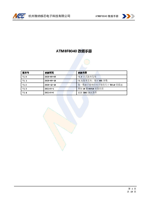
第1共13页页ATM8F8040数据手册版本号更新时间更新内容V1.02020-09-05V1.0正式版本发布V1.12020-09-16V1.1版本发布,修正DNL参数V1.22020-12-10统一数据手册和应用手册的关于T2CAP的描述V1.32021-3-1增加16脚SOP16封装信息V1.42021-3-8更新IDD2测试条件第2页1.主要特色CPU 特性通信8位1T 8051内核支持两路UART 支持1/2/4/8系统分频模拟模块支持双DPTR 支持12路12位ADC 支持双线调试支持上电复位ROM支持低压复位16K 字节FLASH(擦写寿命1000次)时钟128字节EEPROM(擦写寿命10000次)内部时钟频率最高到32MHz,1%精度数据保持时间:10年内部时钟32KHz 低频振荡器RAM支持外部1-20MHz 晶振256字节内部IRAM 工作模式512字节外部XRAM 正常模式GPIO待机模式(IDLE)最多支持18个GPIO 停机模式(Stop),最小电流<1uA 支持任意端口变化中断工作条件Timer/PWM工作频率:最大32MHz 16位8051标准定时器T0/T1工作电压: 2.7~5.5V 带捕获和可编程输出的16位定时器T2工作温度:-40℃~85℃7路16位带互补输出PWM 输出模块封装唤醒Timer 20-TSSOP 看门狗定时器20-QFN 4x4SOP16其他CRC16循环冗余检测模块可配置逻辑计算单元(CPL)外部晶振停振检测1.主要特色 (2)2.概述 (4)2.1.说明 (4)2.2.应用方向 (4)3.设计框图 (4)4.引脚分布图 (5)5.封装尺寸图 (7)5.1.20-TSSOP (7)5.2.20-QFN (8)5.3.SOP16 (9)6.电气特性 (10)6.1.极限参数 (10)6.2.DC特性 (10)6.3.ADC特性 (11)6.4.内部高频振荡器特性 (11)6.5.内部低频振荡器特性 (11)6.6.外部振荡器特性 (12)6.7.存储器工作特性 (12)6.8.外部复位及中断管脚特性 (12)7.芯片选型 (13)2.概述2.1.说明ATM8F8040是一款内嵌16K字节FLASH的8位单片机。

ISP800 SERIES ANNUNCIATOR INSTRUMENTSUSER MANUALISP800 SERIES ANNUNCIATOR INSTRUMENTSUSER MANUAL(*) ModelsISP-24 ISP-32 ISP-36(*) ISP-24, ISP-32, ISP36 are the models of ISP800 series Annunciators representing channels quantity included.Copyright ©2016 by Telepro Energy---------------------------------------------------------------------------------NOTICE---------------------------------------------------------------------------------------Read this manual thoroughly before using ISP800, and store in a safe place for reference. Make sure that this manual is delivered to the final user. The policy of Telepro Enerji is one of continuous improvement.The right is reserved to alter the design on any structural details of the products at any time without giving notice.TABLE OF CONTENTS1. General Overvıew of the Devıce (5)2.Features & Benefits (5)3. C onnectıons (6)3.1. “K” Termınals ( Power Input and Relay Outputs) (6)3.2. Wırıng Scheme (7)3.3. “E” T ermınals ( Rs485 Communication Port ) (10)4. Confıgure Relay Outputs (Horn or Bell ) for All Channels (Mını Confıg Mode) (11)5. Tag Labelıng and Front Panel Installatıon (12)6. Output Relay and Led Status (12)6.1. Alarm States and Relay Outputs (12)6.2. Horn / Sılent Led Status (13)6.3. Safe / Fail Led Status (14)6.4. Input Channels Led Status (14)7. Alarm Sequence ( Modıfıed - ISA-S18.1 Code-M (Manual Reset) ) (15)8. Technıcal Specıfıcatıon (16)9. Maıntenance and Inspectıon (23)10. APPENDIX-1 USER MANUAL REVISION HISTORY (24)11. SERVICE AND TECHNICAL SUPPORT LINE (24)PREFACEPlease read this manual thoroughly before use, and keep the manual at hand for later reference. Also make sure that this manual is delivered to the final users .PRECAUTIONS FOR SAFETYItems to be observed to prevent physical damage and to ensure safe use of this product are noted in this instruction manual.The safety of any system available with the device, is the responsibility of person establishing the system!The device, when used in a manner not specified by the Company, the protection provided by equipment may be impaired.The manufacturer is not responsible for the consequences ifthese conditions are not taken into account.Safety precautions in the manual is considered to be as !! DANGER !!and !! WARNING !!!! DANGER !! : WHEN A DANGEROUS SITUATION MAY OCCURIF HANDLING IS MISTAKEN LEADING FATAL OR MAJOR INJURIES, !! WARNING !! : WHEN A DANGEROUS SITUATION MAY OCCUR IF HANDLING IS MISTAKEN LEADING TO PHYSICAL DAMAGE, DEVICE PERFORMANCE DETERIORATION .!! WARNING !!:PLEASE READ THIS MANUAL CAREFULLY BEFORE PERFORMING ANY OF THE PROCEDURES CONTAINED HEREIN. FAILURE TO FOLLOW THESE INSTRUCTIONS MAY RESULT SEVERE INJURY .!! DANGER !!:HAVE A QUALIFIED ELECTRICAL MAINTENANCE TECHNICIAN INSTALL, ADJUST AND SERVICE THIS EQUIPMENT. FOLLOW THE NATIONAL ELECTRICAL CODE AND ALL OTHER APPLICABLE ELECTRICAL AND SAFETY CODES, INCLUDING THE PROVISIONS OF THE OCCUPATIONAL SAFETY AND HEALTH, WHEN INSTALLING EQUIPMENT.!! DANGER !!: REDUCE THE CHANCE OF AN ELECTRICAL FIRE, SHOCK, OR EXPLOSION BY PROPER GROUNDING, OVER-CURRENT PROTECTION, THERMAL PROTECTION, AND ENCLOSURE. FOLLOW SOUND MAINTENANCE PROCEDURES.!! DANGER !! : CIRCUIT POTENTIALS CAN BE MAX 220VDC . AVOID DIRECT CONTACT WITH THE PRINTED CIRCUIT BOARD OR WITH CIRCUIT ELEMENTS TO PREVENT THE RISK OF SERIOUS INJURY OR FATALITY .!! WARNING !!: DO NOT OPEN THE DEVICE. THERE ARE NOT ANY CONSUMABLE COMPONENTS INSIDE IT.!! WARNING !!: DEVICE SHOULD BE KEPT AWAY FROM HUMIDITY, WET, VIBRATION AND DUSTY ENVIRONMENT. !! WARNING !!: DEVICE SHOULD BE STARTED ONLY IF ALL CONNECTIONS ARE DONE.1.G ENERAL O VERVIEW OF THE D EVICEIn industrial process control, an annunciator panel is a system to alert operators of alarm conditions in the plant. Windows are provided, each engraved with the name of a process alarm. L ED of each window are controlled by hard-wired switches in the plant, arranged to operate when a process condition enters an abnormal state.In one common alarm sequence, the LED near the window will flash, internal buzzer will sound and a bell or horn relay output will be activated so as to external device to sound to attract the operator's attention when the alarm condition is detected. The operator can silence the alarm with a button, and the LED will remain lit as long as the process is in the alarm state. When the alarm clears (process condition returns to normal), the LED goes out.Behavior of alarm systems, and colors used to indicate alarms, are standardized. Standards such as ISA 18.1 simplify purchase of systems and training of operators by giving standard alarm sequences2.F EATURES &B ENEFİTS•The ISP800 Series alarm annunciators that functional, flexible and reliable device are designed to fulfill all the requirements of Alarm condiditons.•Horn or Bell output selection can be easily configurable with pushbuttons for each channels.•Each ISP800 Series annunciator is equipped with low power, long life LEDs. Each alarm point uses RGB LEDs providing illumination in all light conditions Horn/Bell selections and other status.•High Interference Immunity. All alarm inputs are provided with fully isolated inputs using optical couplers and a transient hardware and software filters.•Common Outputs As standard, each unit is fitted with three common relays:Critical Audible Relay (HORN), Non-Critical Audible Relay (BELL), Fault Relay•Integrated audible alarm,•Changeable Printed Legends, can be printed out from any printer.•Low Cost / Compact Design•There are “software programmable” response – release time which provide flexible and safe performance for protection against induced magnetic fields resulted from maneuvers i.e CB opening/closing especially.With the help of ISPSİM TM software;Response and release time are independently set between 3msec and 250msec. Responsetime is set to 5msec, release time is set to 20msec by default•TELEPRO-ISP800, is provided in case configuration, with panel type and in UL94V0_Self-extinguish standard.Mechanical protection of our standard case is of IP51 from the front face. With user friendly screwed mountingsystem, it can be fast and safely mounted / dismantled3.C ONNECTIONSAll connections are made on the rear of the unit using two-part quick disconnect plug in terminals accepting up to 12 AWG (2.5mm2) wires.!! DANGER !! :POWER SUPPLY CONNECTION WITH THE UNIT MUST BE DISCONNECTED COMPLETELY BEFORE ALL MAINTENANCE, REPAIR AND INSTALLATION OPERATIONS.!! DANGER !!:WIRING MUST ALWAYS BE DONE BY A QUALIFIED ELECTRICIAN.!! DANGER !!:ALWAYS INSTALL THE DEVICE BEFORE STARTING WIRING3.1.“K”T ERMINALS (P OWER I NPUT AND R ELAY O UTPUTS)Figure 1-“K “Terminal layouts!! DANGER !!:DURING ALL TERMINAL CONNECTION / DISCONNECTION, POWER SUPPLY CONNECTION MUST BEDISCONNECTED.FAILURE TO DO SO COULD LEAD TO ELECTRICAL SHOCKS OR FIRES.!! DANGER !!:PAY ENOUGH ATTENTION TO THE SUPPLY TERMINALS POLARITY.!! DANGER !!:GND PIN AND SURGE PIN OF INPUT TERMINALS MUST BE SEPERATELY GROUNDED.!! DANGER !!:CONNECT GROUND WIRING THAT COMPLIES WITH THE STANDARDS OF THE COUNTRY WHERE THE UNIT IS BEING INSTALLED. FAILURE TO DO SO COULD LEAD TO DEVICE PERFORMANCE DETERIORATION.3.2.W IRING S CHEMEGND and SURGE must be seperately groundedGND and SURGE must be seperately groundedGND and SURGE must be seperately groundedFigure 6- Terminal block sample connection!! DANGER !! :NOISE FILTERING SURGE TERMINAL SHOULD BE DIRECTLY CONNECTED TO THE PROTECTION EARTH INORDER TO ENABLE PROPER FUNCTIONING OF THE DEVICE.Figure 7!! DANGER !! :WRONG CONNCETION - DO NOT USE ANY JUMPER BETWEEN COM AND SURGE TERMINALS3.3.“E”T ERMINALS (R S485C OMMUNİCATİON P ORT )Figure 8(Required 250ohm termination resistor for master and slave ports, both side of Rs485 comm. line) !! WARNING !!: RS485 COMMUNICATION CABLE MUST BE SCREENED AND SCREENS MUST BE CONNECTED TO GROUND AT ONE END4.C ONFIGURE R ELAY O UTPUTS (H ORN OR B ELL ) FOR A LL C HANNELS (M INI C ONFIG M ODE)I- UnPlug “A” terminal, “B” terminal, “C” terminal and “D” terminalII- Plug in “K” terminal (Supply and relay output)III- After Pluged “K” ternimal, ISP800 runs starup self test procedureIV- Selft test steps are as follows;a-In the first step;All leds are solid and Internal buzzer turns on,“Safe/Fail” led blinks green in 4Hzb-In the second step;Input channel leds and buzzer turn offV- Press Test Button firstly (all input channel leds are solid and buzzer turns on)VI- In order to enter config mode; Press “Test Button” and “Horn Button” together for 3 Sec.VII- After 3 secs laterVII-a- First input channel led blinks in 4HzVII-b- Other input channels leds are offVII-c- “Horn/Silent” led turns off and “Safe/Fail” led blinks green in 4HzVIII-Press Horn Button to setup alarm output type (Horn or Bell ) for input channel 1 while this led blinks in this step. When pressing “Horn Button”,colour of channel 1 led changes to blinking other colour. (Blinking Red means Horn Output / Blinking green means Bell Output)Figure 8IX- Press Test Button to skip to the next input channel. When pressing “test button”, next channel led blinks.X- Press Ack Button to save input channel settings or Press “Reset Button” to cancel configuration settings. When pressing “Ack Button”, ISP800 saves your configuration and restarts up itself.!! WARNING !!: IF ANY BUTTON IS NOT PRESSED FOR 60 SEC IN CONFIG MODE, THEN ISP800 RETURNS TO THE LATEST WORKING PROCESS MODE.Another configuration method is using ISPsim software tool by connecting via RS485 port.You can download ISPsim software from our web site.By following each step explained in ISPsim user manual, you can easiliy configure each channel and changealarm sequence steps or functions from the defaults.5. T AG L ABELING AND F RONT P ANEL I NSTALLATIONWindow for each channel can be named with label template supplied by Telepro. In order to do tag labeling, please follow the order explained in below pictures1,2,3.Whenever requested, labels can be easily changed later.Picture1-Gently hold and unlock front panel frame at one side as shown Picture2-Remove front panel frame from the unitPicture3-Insert tag label into slots as seen belowBefore installing the ISP800 to the Panel,please remove 4pcs of panel mounting sleeves.Then plug -in the unit to the hole on the panel. Fix it to the panel wall with two sides by using 4pcs of panel mounting sleeves provided.And then start wiring according to the scheme provided.6. O UTPUT R ELAY AND L ED S TATUS6.1. A LARM S TATES AND R ELAY O UTPUTSExample1 – Set the first channel to Bell Output (Green Indication),2 – Set the second channel to Horn Output (Red Indication),3 – Press Ack Button and save the configuration and exit,4 – Return to regular working mode.For Channel 1Initial Test Test Fail Process Normal Process Abnormal Horn / Bell Relay Open / Open Open / Open Open / Open Open / Closed Fault Relay (NO/NC) Open /closed Closed/Open Open /closed Open /closed Channel 1 Led Solid Green Off Off Blinking Green 4Hz Horn / Silent Led SolidRed/GreenOffSolid GreenSolid GreenSafe / Fail Led Blinking White/ Solid GreenBlink Red Solid Green Solid GreenFor Channel 2Initial Test Test Fail Process Normal Process Abnormal Horn / Bell Relay Open / Open Open / Open Open / Open Open / Closed Fault Relay (NO/NC) Open /closed Closed/Open Open /closed Open /closed Channel 2 Led Solid Red Off Off Blinking Red 4Hz Horn / Silent Led SolidRed/Green OffSolid GreenSolid Green Safe / Fail LedBlinking White/Solid GreenBlinking RedSolid GreenSolid Green6.2. H ORN / S ILENT L ED S TATUSI- Green BlinkCondition: Unacknowledged Abnormal Process. Result:⇨ Horn / Bell Relays are Turned On⇨ Horn or Bell Relay Outputs or both of them are(CLOSED )Active II- Red BlinkCondition: Unacknowledged Abnormal Process. Result:⇨ Horn / Bell Relays are Turned Off ⇨ H/B Relay Outputs are (OPEN )Passive III- Green SolidCondition: Normal Process/ Acknowledged abnormal proces. Result:⇨ Horn / Bell Relays are Tuned Off⇨ H/B Relay Outputs are (OPEN )Passive IV- Red SolidCondition: Normal Proces /Acknowledged abnormal proces. Result:⇨ Horn / Bell Relays are Tuned Off⇨ H/B Relay Outputs are (OPEN )Passive V- Led Turned OffRelay Outputs in Configuration Mode6.3. S AFE / F AIL L ED S TATUSI- Green BlinkCondition: Manuel configuration mode via push-button settingsII- Red BlinkCondition: Unconfigured / Initial Test Fail,III- Green SolidCondition: In Regular Process Mode Initial test procedures – PASS IV- Red SolidCondition: In Regular Process ModeRelay outputs configuration mode via RS485 Communication (while writing config to ISP) V- Led Turned OffNo Power or Hardware Failure6.4. I NPUT C HANNELS L ED S TATUSI – Solid GreenAcknowledged Alarm, Process :NormalHorn/Bell Relays :Open / OpenII – Solid RedAcknowledged Alarm, Process :NormalHorn/Bell Relays :Open / Open III – Blink Green ( 4Hz)UnAcknowledged Alarm Process :Abnormal Horn/Bell Relays :Open / Closed IV – Blink Red ( 4Hz)UnAcknowledged Alarm Process :Abnormal Horn/Bell Relays :Closed / OpenV – Blink Green ( 2Hz)UnAcknowledged Alarm Process :NormalHorn/Bell Relays :Open / Closed VI – Blink Red ( 2Hz)UnAcknowledged Alarm Process :NormalHorn/Bell Relays :Closed / open VII – Blink Green ( 1Hz)Acknowledged Alarm Process :Abnormal Horn/Bell Relays :Open / Open VIII – Blink Red ( 1Hz)Acknowledged Alarm Process :Abnormal Horn/Bell Relays :Open / OpenIX – Leds are offThere is no alarmCleared all alarms with Reset Button After the acknowledged all alarms.7. A LARM S EQUENCE ( M ODIFIED - ISA-S18.1 C ODE -M (M ANUAL R ESET ) )They are set to Code M “manual reset” by factory default but you can change alarm sequence according to requirements of the application via RS485 port by using ISPsim software tool.8. T ECHNICAL S PECIFICATIONInput TypesOptocoupled, MOV Protected, Transient Filters,sharing common return Input current Per input channel max: 5 mAInput Resistance (min) 15 kΩ for 24/48Vdc ; 57,6 kΩ for 110Vdc;75 kΩ for 110/220VdcInput On/Off VoltagesSurge Withstand Transient to IEC 255.4 1.2/50mS Common Mode: 1kVSeries Mode: 2kVResponse Time Progamble 3-250ms / Default : 5ms Release Time Progamble 3-250ms / Default : 20msVisual7colour (Red -Green-Yellow -Blue-Purple-Turquoise-W hite) RGB led Alarms and other status Audible Integrated 23mm BuzzerHorn / Bell / Fault Relays Integrated 2pcs of FormA Relays (NO) for H/B indication and 1pc of FormC (NO/NC) for system internal fault.Contact Ratings1 A @48Vdc / 0.2 A @250VdcSupply Voltage24/48Vdc (18-60Vdc ); 110Vdc (88-132Vdc ); 110/220Vdc (88-242Vdc )Supply Power10W!! WARNING !!:REINFORCED INSULATION: SHOWS THAT THERE IS NO NEED TO GROUND THE DEVICE BOX .!! WARNING !!:IK CODE (PROTECTION AGAINST MECHANICAL IMPACTS) OF THE DEVICE IS IK07. ENERGY TEST OF 2J IS PERFORMED WITH IMPACT HAMMERPushbuttonsTest -Horn -Ack -Reset -Labeling Changeable Printed Legends,TerminalsScrew-type removable terminals. Maximum wire size: 12 AWG (2.5 mm)Operating Temperature -20°C to +55° C Storage Temperature -25°C to +80° CHumidity 0-95% RH, non condensingCase Flush Panel mounting: 288x144x82,5 mm Protection from the front faceIP51CE Certification EMC- 2009524CEMC ComplianceEN 61000-4-2 (+A1 / +A2 Dielectric Withstand) EN 61000-4-3 (Radiated RFI Immunity) EN 61000-4-4 (Electrical Fast Transient) EN 61000-4-5 (Surge Immunity)EN 61000-4-6 (Conducted RFI Dist. Immunity) EN 61000-4-8 (Radiated Power Freq. Immunity) EN 61000-4-11 (Immunity to voltage dips) EN 61326-1 (Equipment for measurement ) EN 55011 (+A2 Emission – Ind. Sci and Med.)LVD Compliance EN61010-1:2010ISP-24-outline dimensionsISP-32-outline dimensionsISP-36-outline dimensionsMODBUS ADRESS MAPPINGIsp-24/Isp-32/Isp-36 Modbus Register Maps Rev3 Communication Parameters:19200/ 8/ n/ 1 baud rate:19200 / bit :8 / parity bit:no / stop bit :1Requires at least 3ms between answers and query.Basic Registers:Adress (Hex) Read/WriteSection Range Description0x0001 R Bit 0..7 6 Firmware VersionBit 8..15 0x84Model Id = Isp-24 0x83 Model Id = Isp-32 0x8A Model Id = Isp-360x0002 R Bit 0..7 101 Boot (Hardware) Version decimal=101Bit 8..15 0x84Hardware Model Id = Isp-24 0x83 Hardware Model Id = Isp-32 0x8A Hardware Model Id = Isp-360x000F W Bit0..15 0x0001 Channel 1 Toggle Simulation "dec=1"0x0002 Channel 2 Toggle Simulation "dec=2"... ...0x0008 Channel 8 Toggle Simulation "dec=8"... ...0x0012 Channel 18 Toggle Simulation "dec=18"... ...0x0024Channel 36 Toggle Simulation "dec=36"0x0081 Reset Key Press Simulation "dec=129" (single shot) 0x0082 Horn Key Toggle Simulation "dec=130" (toggle)0x0083 Test Key Press Simulation "dec=131" (press)0x0084Acknowledge Key Press Simulation "dec=132" (single shot)0x0085 Test Key De-press Simulation "dec=133"(release)Signal Status Registers:0x0070 or 0x0033 RBit 00/11= Config Eeprom Contents ValidBit 1 1= Configuration Updated since last power cycle Bit 2 1= Front Panel Configuration Mode PendingBit 3 1= Test Mode PendingBit 41= Horn Enabled, 0=Horn DisabledBit 8 1= Output #1 Active (horn)Bit 9 1= Output #2 Active (bell)Bit 11 1= Output #3 (fault)0x0071 R Bit 0 0/1 Input #1 Input Statesor Bit 1 Input #2 0=Normal,0x0034... ... 1=AbnormalBit 15 Input #160x0072 R Bit 0 0/1 Input #1 Activity Register Statesor Bit 1 Input #2 0=Inactive,0x0035 ... ... 1=ActiveBit 15 Input #16 (Indicating not yet Acked by User)0x0073 R Bit 0 0/1 Input #1 Holding Register Statesor Bit 1 Input #2 0=Normal,1=Holding0x0036 ... ... (Indicating already AckedBit 15 Input #16 Abnormal)0x0074R Bit 0 0/1 Input #17 Input Statesor Bit 1 Input #18 0=Normal,0x003F ... ... 1=AbnormalBit 15 Input #320x0075 R Bit 0 0/1 Input #17 Activity Register Statesor Bit 1 Input #18 0=Inactive,0x0040... ... 1=ActiveBit 15 Input #32 (Indicating not yet Acked by User) 0x0076 R Bit 0 0/1 Input #17 Holding Register Statesor Bit 1 Input #18 0=Normal,1=Holding0x0041... ... (Indicating already Acked butBit 15 Input #32 Abnormal)0x0077 R Bit 0 0/1 Input #33 Input Statesor Bit 1 Input #340=Normal,0x004A... ... 1=AbnormalBit 3 Input #360x0078 R Bit 0 0/1 Input #33 Activity Register Statesor Bit 1 Input #340=Inactive,0x004B... ... 1=ActiveBit 3 Input #36 (Indicating not yet Acked by User) 0x0073 R Bit 0 0/1 Input #33 Holding Register Statesor Bit 1 Input #340=Normal,0x004C... ... 1=HoldingBit 3 Input #36 (Indicating already Acked butAbnormal)ISA18.1 Configuration Dependant Registers:Adress (Hex) Read/WriteSection Range Description0x0038 R Bit 0 0/1 Input #1 First Alarm Indication StatesBit 1 Input #2 0=Normal,... ... 1=AlarmBit 15 Input #160x0039 R Bit 0 0/1 Input #1 Momentary Indication StatesBit 1 Input #2 0=Normal,... ... 1=MomentaryBit 15 Input #160x003A R Bit 0 0/1 Input #1 Acknowledged Indication StatesBit 1 Input #2 0=Normal,... ... 1=AcknowledgedBit 15 Input #160x003BR Bit 0 0/1 Input #1 Ringback Indication States Bit 1 Input #2 0=Normal,... ... 1=RingbackBit 15 Input #160x003CR Bit 0 0/1 Input #1 Red Color Indication States Bit 1 Input #2 0=Normal,... ... 1=RedBit 15 Input #160x003D R Bit 0 0/1 Input #1 Green Color Indication StatesBit 1 Input #2 0=Normal,... ... 1=GreenBit 15 Input #160x003E R Bit 0 0/1 Input # Blue Color Indication StatesBit 1 Input # 0=Normal,... ... 1=BlueBit 15 Input #160x0043R Bit 0 0/1 Input #17 First Alarm Indication StatesBit 1 Input #18 0=Normal,... ... 1=AlarmBit 15 Input #320x0044R Bit 0 0/1 Input #17 Momentary Indication StatesBit 1 Input #18 0=Normal,... 1=MomentaryBit 15 Input #320x0045R Bit 0 0/1 Input #17 Acknowledged Indication StatesBit 1 Input #18 0=Normal,... ... 1=AcknowledgedBit 15 Input #320x0046R Bit 0 0/1 Input #17 Ringback Indication StatesBit 1 Input #18 0=Normal,... ... 1=RingbackBit 15 Input #320x0047R Bit 0 0/1 Input #17 Red Color Indication StatesBit 1 Input #18 0=Normal,... ... 1=RedBit 15 Input #320x0048R Bit 0 0/1 Input #17 Green Color Indication StatesBit 1 Input #18 0=Normal,... ... 1=GreenBit 15 Input #320x0049R Bit 0 0/1 Input #17 Blue Color Indication StatesBit 1 Input #18 0=Normal,... ... 1=BlueBit 15 Input #32... (cont.) for only Isp-36 model0x004E R Bit 0 0/1 Input #33 First Alarm Indication StatesBit 1 Input #340=Normal,... ... 1=AlarmBit 3 Input #360x004F R Bit 0 0/1 Input #33 Momentary Indication StatesBit 1 Input #340=Normal,... ... 1=MomentaryBit 3 Input #360x0050 R Bit 0 0/1 Input #33 Acknowledged Indication States Bit 1 Input #340=Normal,... ... 1=AcknowledgedBit 3 Input #360x0051 R Bit 0 0/1 Input #33 Ringback Indication StatesBit 1 Input #340=Normal,... ... 1=RingbackBit 3 Input #360x0052 R Bit 0 0/1 Input #33 Red Color Indication StatesBit 1 Input #340=Normal,... ... 1=RedBit 3 Input #360x0053 R Bit 0 0/1 Input #33 Green Color Indication StatesBit 1 Input #340=Normal,... ... 1=GreenBit 3 Input #360x0054R Bit 0 0/1 Input #33 Blue Color Indication StatesBit 1 Input #340=Normal,... ... 1=BlueBit 3 Input #36Color Codes:Red Bit Green Bit Blue Bit Visible Color0 0 0 Dark / Normal1 0 0 Red0 1 0 Green1 1 0 Yellow0 0 1 Blue1 0 1 Magenta / Purple0 1 1 Sky Blue / Turkuaz1 1 1 WhiteISP-24, ISP -32, ISP36 are the models of ISP800 series Annunciators representing channels quantity included9. M AINTENANCE AND I NSPECTIONThe causes and countermeasuresfor errors are shown in Table-1.Table-1 TroubleshootingINSPECTION IN THE FIELDModel CodeExplanationISP800 ISP-24-MX -DC110 24Channel inputs &2outputs, ModbusRTU, Event recorder, 1000event memory, 110Vdc suppliedISP800 ISP-24-MX -DC110/220 24Channel inputs &2outputs, ModbusRTU, Event recorder, 1000event memory, 110/220Vdc suppliedISP800 ISP-32-MX -DC110 32Channel inputs &2outputs, ModbusRTU, Event recorder, 1000event memory, 110Vdc suppliedISP800 ISP-32-MX -DC110/220 32Channel inputs &2outputs, ModbusRTU, Event recorder, 1000event memory, 110/220Vdc suppliedISP800 ISP-36-MX -DC110 36Channel inputs &2outputs, ModbusRTU, Event recorder, 1000event memory, 110Vdc suppliedISP800ISP-36-MX -DC110/22036Channel inputs &2outputs, ModbusRTU, Event recorder, 1000event memory, 110/220Vdc supplied10.APPENDIX-1USER MANUAL REVISION HISTORY11.SERVICE AND TECHNICAL SUPPORT LINEISP800 contact information for product support is indicated below:800/K -0116-R e v .02r i g h t i s r e s e r v e d t o a l t e r d e s i g n o n a n y s t r u c t u r a l a i l s o f t h e p r o d u c t s a t a n y e w i t h o u t g i v i n g n o t i c e。

SiT8103/2是SiTime 最早推出的小体积,高性能的单端全硅MEMS 振荡器,用于对传统普通石英振荡器的升级与改造,无需改动PCB 设计,管脚100%完全兼容。
不仅可以降低产品成本,改善交货周期,而且从根本上有效解决了石英振荡器所伴随的温漂、一致性差等问题。
SiT8103支持1-110MHZ 任意频点可编程输出,且可精确到小数点后五位数。
内部具有温补功能,全温范围内无温漂,可直接替代石英,整体稳定度可提升10倍以上。
● 1-110MHZ 范围任一频点输出 ● 无温漂、低抖动● 工作电压:1.8V 、2.5V 、2.8V 、3.3V● 工作精度可达±20PPM 、±25PPM 、±30PPM 、±50PPM 、±100PPM ● 兼容LVCMOS/LVTTL 电平输出 ● 工作电流:6.1mA● 具有标准/使能两种工作模式● 同一频点多种封装:2.5×2.0,3.2×2.5,5.0×3.2,7.0×5.0mm ● 全硅半导体工艺,10倍于石英的稳定性 ● 2-4周交货周期应用:● 消费电子、视频、图像采集、机顶盒、HDTV 、DVR 、扫描仪、打印机、复印机、网络摄像头 ●USB1.1、USB2.0、SATA 、SAS 、光端机、IEEE 1394、以太网、PCI 总线等等电气特性表:工作参数 标识最小 典型 最大 单位 测试说明输出频率 f 1 - 110 MHZ频率稳定性F_stab -20 - +20 PPM 此处的精度指工作频偏、温度变化、电压变化、负载变化等条件下的综合考量。
±20PPM 仅限于商规(-20--+70℃)-25 - +25 PPM -30 - +30 PPM -50- +50 PPM老化率 Ag -1.0-+1.0ppM 25℃情况下每年的老化率 工作温度T_use-20 - +70 ℃ 商规 -40 - +85 ℃ 工规 工作电压 Vdd1.71 1.8 1.89 V2.25 2.5 2.75 V 2.52 2.83.08 V 2.973.3 3.63 V工作电流 Idd- 6.7 7.5 mA 无负载,f=20MHZ 、Vdd=2.5V,2.8V or 3.3V -6.16.7mA无负载,f=20MHZ 、Vdd=1.8V■ 特色,优点和应用 ■ 产品简介■ 技术参数工作参数标识最小典型最大单位测试说明静态电流I_std - 2.4 4.3 μA ST=GND, Vdd=3.3V, Output is WeaklyPulled Down- 1.2 2.2 μA ST = GND, Vdd = 2.5V or 2.8V, Output isWeakly Pulled Down- 0.4 0.8 μA ST=GND, Vdd=1.8V, Output is WeaklyPulled Down占空因数DC 45 50 55 % All Vdds. F<=75MHZ40 50 60 % All Vdds. F>75MHZ上升/下降时间Tr,Tf - 1 2 ns 20%--80% Vdd=2.5v,2.8v or 3.3v15pF Load- 1.3 2.5 ns 20%--80% Vdd=1.8v 15pF Load输出高电平VOH 90% - - Vdd IOH=-4mA (Vdd=3.3v)IOH=-3mA (Vdd=2.8v or 2.5v)IOH=-2mA (Vdd=1.8v)输出低电平VOL - - 10% Vdd IOL=4mA (Vdd=3.3v)IOL=3mA (Vdd=2.8v or 2.5v)IOL=2mA (Vdd=1.8v)输出负载Output load Ld - - 15PF At maximum frequency and supplyvoltage.Contact SiTime for higheroutput load option输入高电平VIH 70% - - Vdd Pin 1,OE or ST输入低电平VIL - - 30% Vdd Pin 1,OE or ST建立时间Startup TimeT_osc - - 10 ms 如下图1所示恢复时间Resume TimeT_resume - 3.0 4 ms 如下图1所示周期抖动T_jitt - - 4.0 ps f=75MHZ,Vdd=2.5V,2.8V or 3.3V- - 6.5 ps f=75MHZ,Vdd=1.8V相位抖动T_phj - 0.6 - ps f=75MHZ,测试带宽:900Khz to 7.5MHZ,Vdd=2.5V,2.8V or 3.3V.- 0.8 - ps f=75MHZ,测试带宽:900Khz to 7.5MHZ,Vdd=1.8V.图1管脚说明:OE 模式:当1脚为高或悬空时,正常输出CLK 信号; 当1脚为低时,输出禁止,呈高阻状态。


Key SpecificationsSI-8008TM (ADJ Type)SI-8033TMSI-8050TMSI-8120TM6 O u t p u t V o l t a g e V O [V ]2 4 6 8 10入力電圧 V IN [V]Output Current I O [A]20 40 60 80 100 120 140 160 180Junction Temperature Tj [℃]Io=0ATSD OFF TSD ONI O =0A 、0.1A 0.5A 1.0A 1.5A0.2 0.4 0.60.8 1.0 1.2 1.4 1.60 10 20 30 40Vss=0V(4) Circuit Current at Output OFF10 20 30 40入力電圧 V IN [V]8 6 4 2(6) Thermal Protection V IN =8V Io=0.01AV IN =40V30V20V 15v10V8V5 4 3 2 10 400 300 2001006 5 4 3 2Note1:As the efficiency varies subject to the input voltage and output current, it shall be obtained from the efficiency curve in page 4 and substituted in percent. Note2:Thermal design for Di shall be made separately.−⎟⎟⎠⎞⎜⎜⎝⎛−⋅=x O O D V I V P 1100ηV V I ηV copper areaGlass ‐epoxy board mounting in 30×30㎜SI-8000TM Series Power DissipationTjmax=125℃Ambient Temperature Ta [℃]copper areacopper areacopper areacopper areacopper areaBDCB:MIN 1.60C:13.0±0.54.0±0.12.0±0.11.77.5016.010.50.3φ1.70.30.257.12.65φ1.58.0Direction of Reel9.Cautions and warnings9-1 Parallel operationThe parallel operation to increase the current is not available.9-2 Thermal protectionThe SI-8000TM series has a thermal protection circuit. This circuit keeps the IC from the fever by the over load. But this circuit cannot guarantee the long-term reliability against the continuously over load status.CAUTION / WARNING●The information in this publication has been carefully checked and is believed to be accurate; however, no responsibility is assumed for inaccuracies.● Sanken reserves the right to make changes without further notice to any products herein in the interest of improvements in the performance, reliability, or manufacturability of its products.Before placing an order, Sanken advises its customers to obtain the latest version of the relevant information to verify that the information being relied upon is current.● Application and operation examples described in this catalog are quoted for the sole purpose of reference for the use of the products herein and Sanken can assume no responsibility for any infringement of industrial property rights, intellectual property rights or any other rights of Sanken or any third party which may result from its use.● When using the products herein, the applicability and suitability of such products for the intended purpose or object shall be reviewed at the users’ responsibility.● Although Sanken undertakes to enhance the quality and reliability of its products, the occurrence of failure nd defect of semiconductor products at a certain rate is inevitable. Users of Sanken products are requested to take, at their own risk, preventative measures including safety design of the equipment or systems against any possible injury, death, fires or damages to the society due to device failure or malfunction.● Sanken products listed in this catalog are designed and intended for the use as components in general purpose electronic equipment or apparatus (home appliances, office equipment, telecommunication equipment, measuring equipment, etc.). Before placing an order, the user’s written consent to the specifications is requested.When considering the use of Sanken products in the applications where higher reliability is required (transportation equipment and its control systems, traffic signal control systems or equipment, fire/crime alarm systems, various safety devices, etc.), please contact your nearest Sanken sales representative to discuss and obtain written confirmation of your specifications. The use of Sanken products without the written consent of Sanken in the applications where extremely high reliability is required (aerospace equipment, nuclear power control systems, life support systems, etc.) is strictly prohibited.● Anti radioactive ray design is not considered for the products listed herein.● This publication shall not be reproduced in whole or in part without prior written approval from Sanken.●This is notification that you, as purchaser of the products/technology, are not allowed to perform any of the following:1. Resell or retransfer these products/technology to any party intending to disturb international peace and security.2. Use these products/technology yourself for activities disturbing international peace and security.3. Allow any other party to use these products/technology for activities disturbing international peace and security. Also, as purchaser of these products/technology, you agree to follow the procedures for the export or transfer of these products/technology, under the Foreign Exchange and Foreign Trade Law, when you export or transfer the products/technology abroad.。

TF8008自愈环光端机用户手册目录一.系统概述 (1)二.主要特点 (1)三.技术参数 (2)3.1. 光接口 (2)3.2. 以太网接口 (2)3.3. 供电条件 (3)3.4. 工作环境 (3)3.5. 外形尺寸 (3)四.指示灯定义 (3)五.接口定义 (4)5.1. 光接口定义 (4)5.2. 网口定义 (4)5.3. 串口定义 (4)六.典型应用 (4)七.设备安装 (5)7.1. 设备安装 (5)7.2. 设备测试 (6)八.随机配件 (6)九.产品保修 (6)一.系统概述TF8008系列产品是高性能的嵌入式工业以太网自愈环光端机,全线速1000M 冗余光纤环网结构, 可以实现多点以太网接口的光纤环网传输与接入。
该光端机采用大规模专业集成电路,高集成光收发器件及数字锁相环技术,小体积,高可靠性,支持256个光纤节点,各从站故障、掉电、断纤时自动切除,故障恢复后自动投入。
切换时间小于20ms。
自愈判据依次为收无光,E3误码,E6误码,提高了系统稳定性和安全性。
支持多种协议。
是专门为电力配网自动化、工业自动化、交通、电信等工业高可靠数据通信而设计。
解决了通讯距离远与通讯速率高、节点多且分散的矛盾,同时也解决了电磁干扰、地环干扰和雷电破坏的难题,大大节约了光纤资源。
该自愈环光端机有2路全线速1000M冗余光纤接口,用户接口有8路10/100M 自适应以太网接口,网口具备限速、VLAN、优先级配置。
公司自发研制的2路全线速1000M冗余光纤以太网交换机可髙质量传输H.264髙清视频信号,由该光端机组建的光纤环网支持256个光纤节点,累计可传输H.264髙清视频信号多达300路及其它控制采集信号,决了传统点对点光纤传输中光纤资源的浪费及组网复杂髙成本等问题。
是安防、智能交通、平安城市、高速公路光纤组网首先方案。
设备采用豪华迷你铝机箱设计。
外形简洁、美观。
外部供电为直流DC5V~DC24V 或交流AC220V可选方式。


MODEL TS8008 - 8" COLOR TOUCHSCREENBulletin HP471055U008 Issue 1.0Drawing No. LP0876X Effective 10/11Each option card comes with a cable for communications and threescrews for attaching the option card to the TS’s main board.To install the option card, remove all power and I/O communicationscables from the unit and remove the rear cover. Connect the cable from theoption card to the connector on the main board. Be sure both ends of thecable are firmly seated into their appropriate connector housings. Use thethree screws provided to mount the option card to the main board as shownin Figure 1.Carefully replace the rear cover by reversing the instructions forremoving the rear cover.TYPICAL EXPANSION CARD INSTALLATIONFigure 1DH485 COMMUNICATIONSThe TS8008’s RS422/485 COMMS port can also be used for Allen Bradley DH485 communications.WARNING : DO NOT use a standard DH485 cable to connect this port to Allen Bradley equipment.1. The operator interface is shipped without a configuration. After downloading a configuration, if the light remains in the flashing state continuously, try cycling power. If the LED still continues to flash, try downloading a configuration again.2. Do not turn off power to the unit while this light is flickering. The unit writes data in two minute intervals. Later Microsoft operating systems will not lock the drive unless they need to write data; Windows 98 may lock the drive any time it is mounted, thereby interfering with logging. Refer to “Mounting the CompactFlash” in the DSI8000 User Manual.BATTERY & TIME KEEPINGA battery is used to keep time when the unit is without power. Typical accuracy of the TS8008 time keeping is less than one minute per month drift. The battery of a TS8008 unit does not affect the unit’s memory, all configurations and data is stored in non-volatile memory.To change the battery of a TS8008, remove power, cabling, and then the rear cover of the unit. To remove the cover, remove the five screws designated by the arrows on the rear of the unit. Then, by lifting the top side, hinge the cover, thus providing clearance for the connectors on the bottom side of the PCB as shown in the illustration below. Install in the reverse manner.Remove the old battery* from the holder and replace with the new battery. Replace the rear cover, cables, and re-apply power. Using DSI8000 or the unit’s keypad, enter the correct time and date.* Please note that the old battery must be disposed of in a manner that complies with your local waste regulations. Also, the battery must not be disposed of in fire, or in a manner whereby it may be damaged and its contents come into contact with human skin.The battery used by the TS8008 is a lithium type CR2025.OPTIONAL COMMUNICATION CARDParker - SSD Drives offers optional communication cards for fieldbus communications. These communication cards will allow your TS8008 to communicate with many of the popular fieldbus protocols.COMPACTFLASH SOCKETCompactFlash socket is a Type II socket that can accept either Type I or II cards. Use cards with a minimum of 4 Mbytes and a maximum of 2 Gbytes with the TS8008’s CompactFlash socket. Cards are available at most computer and office supply retailers.CompactFlash can be used for configuration transfers, larger configurations, data logging, and trending.Information stored on a CompactFlash card by a TS8008 can be read by a card reader attached to a PC. This information is stored in IBM (Windows ®) PC compatible FAT16 file format.Parker Hannifin CorporationSSD Drives Division 9225 Forsyth Park Dr.Charlotte, NC 28273 USA Tel: (704) 588-3246Fax: (704) /usa **********************。


目录电源类(1-10)8.CSD19535 (18)9.INA210 (19)10.INA282 (21)1.TPS28225 (2)7.TPS4021 (16)3.TPS54340 (5)4.TPS56528 (9)5.TPS7A1601 (12)6.TPS7A4001 (14)2.UCC27211 (4)高速放大器(11-17)15.LMH6552 (31)12.LMH6703 (25)17.OPA2356 (34)13.OPA2695 (27)16.OPA842 (32)11.THS3201 (23)14.VCA821 (29)精密ADC/DAC (18-21)18.ADS1118 (36)19.DAC7811 (38)20.DAC8571 (41)21.REF3330 (43)精密放大器(22-27)22.INA333 (45)23.INA826 (46)24.OPA192 (48)25.OPA2320 (50)26.OPA2330 (52)27.OPA2376 (53)音频功放(28)28.TPA3112 (55)其他(29-33)30.SN74AUP1G07 (58)29.TLV3501 (57)33.TS12A4515 (62)31.TS5A3159 (61)32.TS5A3166 (62)零一.TPS282258引脚高频4A吸入电流同步MOSFET驱动器描述The TPS28225 and TPS28226 are high-speed drivers for N-channel complimentary driven power MOSFETs with adaptive dead-time control. These drivers are optimized for use in variety of high-current one and multi-phase dc-to-dc converters. The TPS28225/6 is a solution that provides highly efficient, small size low EMI emmissions.The performance is achieved by up to 8.8-V gate drive voltage, 14-ns adaptive dead-time control, 14-ns propagation delays and high-current 2-A source and 4-A sink drive capability. The 0.4-impedance for the lower gate driver holds the gate of power MOSFET below its threshold and ensures no shoot-through current at high dV/dt phase node transitions. The bootstrap capacitor charged by an internal diode allows use of N-channel MOSFETs in half-bridge configuration.The TPS28225/6 features a 3-state PWM input compatible with all multi-phase controllers employing 3-state output feature. As long as the input stays within 3-state window for the 250-ns hold-off time, the driver switches both outputs low. This shutdown mode prevents a load from the reversed- output-voltage.The other features include under voltage lockout, thermal shutdown and two-way enable/power good signal. Systems without 3-state featured controllers can use enable/power good input/output to hold both outputs low during shutting down.The TPS28225/6 is offered in an economical SOIC-8 and thermally enhanced low-size Dual Flat No-Lead (DFN-8) packages. The driver is specified in the extended temperature range of –40°C to 125°C with the absolute maximum junction temperature 150°C. The TPS28226 operates in the same manner as the TPS28225/6 other than the input under voltage lock out. Unless otherwise stated all references to the TPS28225 apply to the TPS28226 also.特性Drives Two N-Channel MOSFETs with 14-ns Adaptive Dead TimeWide Gate Drive Voltage: 4.5 V Up to 8.8 V With Best Efficiency at 7 V to 8 V Wide Power System Train Input Voltage: 3 V Up to 27 VWide Input PWM Signals: 2.0 V up to 13.2-V AmplitudeCapable Drive MOSFETs with ≥40-A Current per PhaseHigh Frequency Operation: 14-ns Propagation Delay and10-ns Rise/Fall Time Allow FSW - 2 MHzCapable Propagate <30-ns Input PWM PulsesLow-Side Driver Sink On-Resistance (0.4 ) Prevents dV/dT Related Shoot-Through Current 3-State PWM Input for Power Stage Shutdown Space Saving Enable (input) and Power Good (output) Signals on Same Pin Thermal Shutdown UVLO Protection Internal Bootstrap Diode Economical SOIC-8 and Thermally Enhanced 3-mm x 3-mm DFN-8 Packages High Performance Replacement for Popular 3-State Input Drivers APPLICATIONS Multi-Phase DC-to-DC Converters with Analog or Digital Control Desktop and Server VRMs and EVRDs Portable/Notebook Regulators Synchronous Rectification for Isolated Power Supplies参数零二.UCC27211120V 升压4A 峰值电流的高频高侧/低侧驱动器 描述UCC27210 和 UCC27211 驱动器基于常见的 UCC27200 和 UCC27201 MOSFET 驱动器,但是对性能进行了几项重大改进。