MAX3244CWI+中文资料
- 格式:pdf
- 大小:458.26 KB
- 文档页数:22
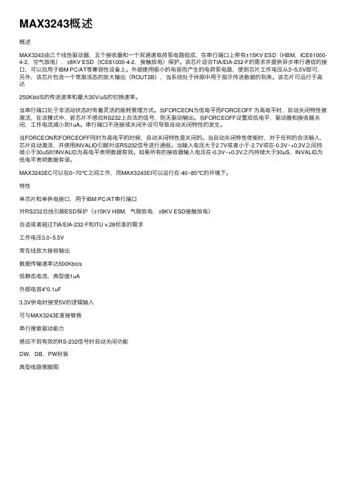
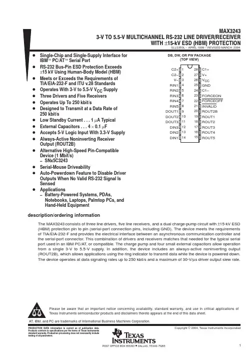
MAX3243概述概述MAX3243由三个线性驱动器,五个接收器和⼀个双通道电荷泵电路组成,在串⾏端⼝上带有±15KV ESD(HBM,ICE61000-4-2,空⽓放电),±8KV ESD(ICE61000-4-2,接触放电)保护。
该芯⽚迎合TIA/EIA-232-F的需求并提供异步串⾏通信的接⼝,可以应⽤于IBM PC/AT等兼容性设备上。
外部使⽤极⼩的电容⽽产⽣的电荷泵电路,使到芯⽚⼯作电压从3~5.5V即可,另外,该芯⽚包含⼀个常激活态的放⼤输出(ROUT2B),当系统处于休眠中⽤于指⽰传送数据的到来。
该芯⽚可运⾏于⾼达250Kbit/S的传送速率和最⼤30V/uS的切换速率。
当串⾏端⼝处于⾮活动状态时有着灵活的能耗管理⽅式。
当FORCEON为低电平⽽FORCEOFF 为⾼电平时,⾃动关闭特性被激活,在该模式中,若芯⽚不感应RS232上合法的信号,则⽆驱动输出。
当FORCEOFF设置成低电平,驱动器和接收器关闭,⼯作电流减⼩到1uA。
串⾏端⼝不连接或关闭外设可导致⾃动关闭特性的发⽣。
当FORCEON和FORCEOFF同时为⾼电平的时候,⾃动关闭特性是关闭的。
当⾃动关闭特性使能时,对于任何的合法输⼊,芯⽚⾃动激活,并使⽤INVALID引脚对该RS232信号进⾏通报。
当输⼊电压⼤于2.7V或者⼩于-2.7V或在-0.3V~+0.3V之间持续⼩于30uS时INVALID为⾼电平表明数据有效。
如果所有的接收器输⼊电压在-0.3V~+0.3V之内持续⼤于30uS,INVALID为低电平表明数据有误。
MAX3243EC可以在0~70℃之间⼯作,⽽MAX3243EI可以运⾏在-40~85℃的环境下。
特性单芯⽚和单供电接⼝,⽤于IBM PC/AT串⾏端⼝对RS232总线引脚ESD保护(±15KV HBM,⽓隙放电,±8KV ESD接触放电)合适或者超过TIA/EIA-232-F和ITU v.28标准的需求⼯作电压3.0~5.5V常在线放⼤接收输出数据传输速率达500Kbit/s低静态电流,典型值1uA外部电容4*0.1uF3.3V供电时接受5V的逻辑输⼊可与MAX3243E直接替换串⾏搜索驱动能⼒感应不到有效的RS-232信号时⾃动关闭功能DW,DB,PW封装典型电路管脚图。
LM324中文资料大全来源:21ic作者:LM324系列器件带有真差动输入的四运算放大器。
与单电源应用场合的标准运算放大器相比,它们有一些显著优点。
该四放大器可以工作在低到 3.0伏或者高到32伏的电源下,静态电流为MC1741的静态电流的五分之一。
共模输入范围包括负电源,因而消除了在许多应用场合中采用外部偏置元件的必要性。
每一组运算放大器可用图1所示的符号来表示,它有5个引出脚,其中“+”、“-”为两个信号输入端,“V+”、“V-”为正、负电源端,“Vo”为输出端。
两个信号输入端中,Vi-(-)为反相输入端,表示运放输出端Vo的信号与该输入端的位相反;Vi+(+)为同相输入端,表示运放输出端Vo的信号与该输入端的相位相同。
LM324系列由四个独立的,高增益,内部频率补偿运算放大器,其中专为从单电源供电的电压范围经营。
从分裂电源的操作也有可能和低电源电流消耗是独立的电源电压的幅度。
应用领域包括传感器放大器,直流增益模块和所有传统的运算放大器现在可以更容易地在单电源系统中实现的电路。
例如,可直接操作的LM324系列,这是用来在数字系统中,轻松地将提供所需的接口电路,而无需额外的±15V电源标准的5V电源电压。
运放类型:低功率放大器数目:4带宽:1.2MHz针脚数:14工作温度范围:0°C to +70°C封装类型:SOIC3dB带宽增益乘积:1.2MHz变化斜率:0.5V/μs器件标号:324器件标记:LM324AD增益带宽:1.2MHz工作温度最低:0°C工作温度最高:70°C放大器类型:低功耗温度范围:商用电源电压最大:32V电源电压最小:3V芯片标号:324表面安装器件:表面安装输入偏移电压最大:7mV运放特点:高增益频率补偿运算逻辑功能号:324额定电源电压, +:15V1.短路保护输出2.真差动输入级3.可单电源工作:3V-32V4.低偏置电流:最大100nA5.每封装含四个运算放大器。
LM324中文资料大全LM324系列器件带有真差动输入的四运算放大器。
与单电源应用场合的标准运算放大器相比,它们有一些显著优点。
该四放大器可以工作在低到3.0伏或者高到32伏的电源下,静态电流为MC1741的静态电流的五分之一。
共模输入范围包括负电源,因而消除了在许多应用场合中采用外部偏置元件的必要性。
每一组运算放大器可用图1所示的符号来表示,它有5个引出脚,其中“+”、“-”为两个信号输入端,“V+”、“V-”为正、负电源端,“Vo”为输出端。
两个信号输入端中,Vi-(-)为反相输入端,表示运放输出端Vo的信号与该输入端的位相反;Vi+(+)为同相输入端,表示运放输出端Vo的信号与该输入端的相位相同。
LM324系列由四个独立的,高增益,内部频率补偿运算放大器,其中专为从单电源供电的电压范围经营。
从分裂电源的操作也有可能和低电源电流消耗是独立的电源电压的幅度。
应用领域包括传感器放大器,直流增益模块和所有传统的运算放大器现在可以更容易地在单电源系统中实现的电路。
例如,可直接操作的LM324系列,这是用来在数字系统中,轻松地将提供所需的接口电路,而无需额外的±15V电源标准的5V电源电压。
运放类型:低功率放大器数目:4带宽:1.2MHz针脚数:14工作温度范围:0°C to +70°C封装类型:SOIC3dB带宽增益乘积:1.2MHz变化斜率:0.5V/μs器件标号:324器件标记:LM324AD增益带宽:1.2MHz工作温度最低:0°C工作温度最高:70°C放大器类型:低功耗温度范围:商用电源电压最大:32V电源电压最小:3V芯片标号:324表面安装器件:表面安装输入偏移电压最大:7mV运放特点:高增益频率补偿运算逻辑功能号:324额定电源电压, +:15V1.短路保护输出2.真差动输入级3.可单电源工作:3V-32V4.低偏置电流:最大100nA5.每封装含四个运算放大器。
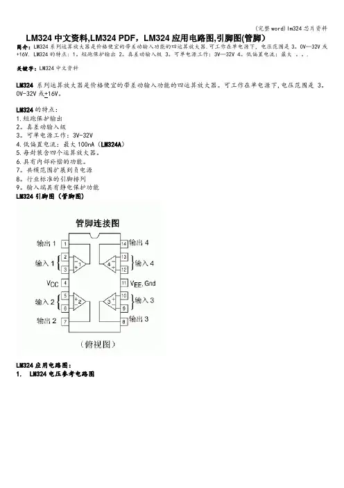
LM324中文资料,LM324 PDF,LM324应用电路图,引脚图(管脚)
简介:LM324系列运算放大器是价格便宜的带差动输入功能的四运算放大器.可工作在单电源下,电压范围是3。
0V—32V或+16V. LM324的特点: 1。
短跑保护输出 2。
真差动输入级 3。
可单电源工作:3V—32V 4。
低偏置电流:最大。
.
关键字:LM324中文资料
LM324系列运算放大器是价格便宜的带差动输入功能的四运算放大器。
可工作在单电源下,电压范围是3。
0V-32V或+16V。
LM324的特点:
1.短跑保护输出
2。
真差动输入级
3。
可单电源工作:3V-32V
4.低偏置电流:最大100nA(LM324A)
5.每封装含四个运算放大器。
6.具有内部补偿的功能。
7。
共模范围扩展到负电源
8。
行业标准的引脚排列
9。
输入端具有静电保护功能
LM324引脚图(管脚图)
LM324应用电路图:
1. LM324电压参考电路图
2. LM324多路反馈带通滤波器电路图
3. LM324高阻抗差动放大器电路图
4. LM324函数发生器电路图
5. LM324双四级滤波器
6。
LM324维思电桥振荡器电路图
7。
LM324滞后比较器电路图。
元器件交易网IMPORTANT NOTICETexas Instruments and its subsidiaries (TI) reserve the right to make changes to their products or to discontinueany product or service without notice, and advise customers to obtain the latest version of relevant informationto verify, before placing orders, that information being relied on is current and complete. All products are soldsubject to the terms and conditions of sale supplied at the time of order acknowledgement, including thosepertaining to warranty, patent infringement, and limitation of liability.TI warrants performance of its semiconductor products to the specifications applicable at the time of sale inaccordance with TI’s standard warranty. Testing and other quality control techniques are utilized to the extentTI deems necessary to support this warranty. Specific testing of all parameters of each device is not necessarilyperformed, except those mandated by government requirements.CERTAIN APPLICATIONS USING SEMICONDUCTOR PRODUCTS MAY INVOLVE POTENTIAL RISKS OFDEATH, PERSONAL INJURY, OR SEVERE PROPERTY OR ENVIRONMENTAL DAMAGE (“CRITICALAPPLICATIONS”). TI SEMICONDUCTOR PRODUCTS ARE NOT DESIGNED, AUTHORIZED, ORWARRANTED TO BE SUITABLE FOR USE IN LIFE-SUPPORT DEVICES OR SYSTEMS OR OTHERCRITICAL APPLICATIONS. INCLUSION OF TI PRODUCTS IN SUCH APPLICATIONS IS UNDERSTOOD TOBE FULLY AT THE CUSTOMER’S RISK.In order to minimize risks associated with the customer’s applications, adequate design and operatingsafeguards must be provided by the customer to minimize inherent or procedural hazards.TI assumes no liability for applications assistance or customer product design. TI does not warrant or representthat any license, either express or implied, is granted under any patent right, copyright, mask work right, or otherintellectual property right of TI covering or relating to any combination, machine, or process in which suchsemiconductor products or services might be or are used. TI’s publication of information regarding any thirdparty’s products or services does not constitute TI’s approval, warranty or endorsement thereof.Copyright © 2000, Texas Instruments Incorporated。
General DescriptionThe MAX3222E/MAX3232E/MAX3237E/MAX3241E are 3V-powered EIA/TIA-232 and V.28/V.24 communications interfaces with low power requirements, high data-rate capabilities, and enhanced electrostatic discharge (ESD)protection. All transmitter outputs and receiver inputs are protected to ±15kV using IEC 1000-4-2 Air-G ap Discharge, ±8kV using IEC 1000-4-2 Contact Discharge,and ±15kV using the Human Body Model. In addition, the MAX3237E’s logic and receiver I/O pins are protected to the above ESD standards.The transceivers have a proprietary low-dropout transmit-ter output stage, delivering true RS-232 performance from a +3.0V to +5.5V supply with a dual charge pump. The charge pump requires only four small 0.1µF capacitors for operation from a +3.3V supply. Each device is guaran-teed to run at data rates of 250kbps while maintaining RS-232 output levels. The MAX3237E is guaranteed to run at data rates of 250kbps in the normal operating mode and 1Mbps in the MegaBaud™ operating mode while main-taining RS-232-compliant output levels.The MAX3222E/MAX3232E have two receivers and two drivers. The MAX3222E features a 1µA shutdown mode that reduces power consumption and extends battery life in portable systems. Its receivers can remain active in shutdown mode, allowing external devices such as modems to be monitored using only 1µA supply current.Both the MAX3222E and MAX3232E are pin, package,and functionally compatible with the industry-standard MAX242 and MAX232, respectively.The MAX3241E is a complete serial port (three drivers/five receivers) designed for notebook and sub-notebook computers. The MAX3237E (five drivers/three receivers) is ideal for peripheral applications that require fast data transfer. Both devices feature a shutdown mode in which all receivers can remain active while using a supply current of only 1µA (MAX3241E) or 10nA (MAX3237E). The MAX3237E/MAX3241E have additional receiver outputs that always remain active.The MAX3222E, MAX3232E, and MAX3241E are avail-able in space-saving SO, SSOP, and TSSOP packages.The MAX3237E is available in an SSOP package.________________________ApplicationsBattery-Powered Equipment PrintersCell PhonesSmart Phones Cell-Phone Data Cables xDSL ModemsNotebook, Subnotebook, and Palmtop ComputersFeatureso ESD Protection for RS-232 I/O Pins(MAX3222E/MAX3232E/MAX3237E/MAX3241E)±15kV—Human Body Model±8kV—IEC 1000-4-2, Contact Discharge ±15kV—IEC 1000-4-2, Air-Gap Discharge o ESD Protection For All Logic and Receiver I/O Pins (MAX3237E)±15kV—Human Body Model±8kV—IEC 1000-4-2, Contact Discharge ±15kV—IEC 1000-4-2, Air-Gap Discharge o Guaranteed Data Rate250kbps (MAX3222E/MAX3232E/MAX3241E and MAX3237E, Normal Operation)1Mbps (MAX3237E, MegaBaud Operation)o Latchup Freeo Low-Power Shutdown with Receivers Active1µA (MAX3222E/MAX3241E)10nA (MAX3237E)o Flow-Through Pinout (MAX3237E)o Guaranteed Mouse Driveability (MAX3241E)o Meets EIA/TIA-232 Specifications Down to 3.0VMAX3222E/MAX3232E/MAX3237E/MAX3241E †±15kV ESD-Protected, Down to 10nA, 3.0V to 5.5V ,Up to 1Mbps, True RS-232 Transceivers________________________________________________________________Maxim Integrated Products119-1298; Rev 5; 3/02MegaBaud is a trademark of Maxim Integrated Products, Inc.†Covered by U.S. Patent numbers 4,636,930; 4,679,134; 4,777,577; 4,797,899; 4,809,152; 4,897,774; 4,999,761; and other patents pending.For pricing, delivery, and ordering information,please contact Maxim/Dallas Direct!at 1-888-629-4642, or visit Maxim’s website at .M A X 3222E /M A X 3232E /M A X 3237E /M A X 3241E±15kV ESD-Protected, Down to 10nA, 3.0V to 5.5V ,Up to 1Mbps, True RS-232 TransceiversABSOLUTE MAXIMUM RATINGSELECTRICAL CHARACTERISTICSStresses beyond those listed under “Absolute Maximum Ratings” may cause permanent damage to the device. These are stress ratings only, and functional operation of the device at these or any other conditions beyond those indicated in the operational sections of the specifications is not implied. Exposure to absolute maximum rating conditions for extended periods may affect device reliability.V CC to GND..............................................................-0.3V to +6V V+ to GND (Note 1)..................................................-0.3V to +7V V- to GND (Note 1)...................................................+0.3V to -7V V+ + |V-| (Note 1).................................................................+13V Input VoltagesT_IN, EN , SHDN , MBAUD to GND ........................-0.3V to +6V R_IN to GND.....................................................................±25V Output VoltagesT_OUT to GND...............................................................±13.2V R_OUT, R_OUTB (MAX3241E)................-0.3V to (V CC + 0.3V)Short-Circuit Duration, T_OUT to GND.......................Continuous Continuous Power Dissipation (T A = +70°C)16-Pin SSOP (derate 7.14mW/°C above +70°C)..........571mW 16-Pin Wide SO (derate 9.52mW/°C above +70°C).....762mW18-Pin Wide SO (derate 9.52mW/°C above +70°C).....762mW 18-Pin PDIP (derate 11.11mW/°C above +70°C)..........889mW 20-Pin TSSOP (derate 10.9mW/°C above +70°C)........879mW 20-Pin SSOP (derate 8.00mW/°C above +70°C)..........640mW 28-Pin SSOP (derate 9.52mW/°C above +70°C)..........762mW 28-Pin Wide SO (derate 12.50mW/°C above +70°C).............1W 28-Pin TSSOP (derate 12.8mW/°C above +70°C)......1026mW 32-pin QFN (derate 23.2mW/°C above +70°C).............1860mW Operating Temperature RangesMAX32_ _EC_ _...................................................0°C to +70°C MAX32_ _EE_ _.................................................-40°C to +85°C Storage Temperature Range.............................-65°C to +150°C Lead Temperature (soldering, 10s).................................+300°CNote 1:V+ and V- can have maximum magnitudes of 7V, but their absolute difference cannot exceed 13V.MAX3222E/MAX3232E/MAX3237E/MAX3241E±15kV ESD-Protected, Down to 10nA, 3.0V to 5.5V ,Up to 1Mbps, True RS-232 TransceiversELECTRICAL CHARACTERISTICS (continued)(V CC = +3.0V to +5.5V, C1–C4 = 0.1µF, T A = T MIN to T MAX , unless otherwise noted. Typical values are at T A = +25°C.) (Note 2)(V CC = +3.0V to +5.5V, C1–C4 = 0.1µF, T A = T MIN to T MAX , unless otherwise noted. Typical values are at T A = +25°C.) (Note 2)__________________________________________Typical Operating Characteristics(V CC = +3.3V, 250kbps data rate, 0.1µF capacitors, all transmitters loaded with 3k Ωand C L , T A = +25°C, unless otherwise noted.)-6-5-4-3-2-10123456010002000300040005000MAX3222E/MAX3232ETRANSMITTER OUTPUT VOLTAGEvs. LOAD CAPACITANCELOAD CAPACITANCE (pF)T R A N S M I T T E R O U T P U T V O L T A G E (V )624108141216010002000300040005000MAX3222E/MAX3232ESLEW RATE vs. LOAD CAPACITANCELOAD CAPACITANCE (pF)S L E W R A T E (V /µs )2520155103530404520001000300040005000MAX3222E/MAX3232E OPERATING SUPPLY CURRENT vs. LOAD CAPACITANCELOAD CAPACITANCE (pF)S U P P L Y C U R R E N T (m A )M A X 3222E /M A X 3232E /M A X 3237E /M A X 3241E±15kV ESD-Protected, Down to 10nA, 3.0V to 5.5V ,Up to 1Mbps, True RS-232 Transceivers4_______________________________________________________________________________________TIMING CHARACTERISTICS —MAX3237ENote 2:MAX3222E/MAX3232E/MAX3241E: C1–C4 = 0.1µF tested at 3.3V ±10%; C1 = 0.047µF, C2, C3, C4 = 0.33µF tested at 5.0V±10%. MAX3237E: C1–C4 = 0.1µF tested at 3.3V ±5%, C1–C4 = 0.22µF tested at 3.3V ±10%; C1 = 0.047µF, C2, C3, C4 =0.33µF tested at 5.0V ±10%.Note 3:The MAX3237E logic inputs have an active positive feedback resistor. The input current goes to zero when the inputs are atthe supply rails.Note 4:Transmitter skew is measured at the transmitter zero crosspoints.MAX3222E/MAX3232E/MAX3237E/MAX3241E±15kV ESD-Protected, Down to 10nA, 3.0V to 5.5V ,Up to 1Mbps, True RS-232 Transceivers_______________________________________________________________________________________5-6-2-42046-5-31-135010001500500200025003000LOAD CAPACITANCE (pF)T R A N S M I T T E R O U T P U T V O L T A G E (V )MAX3237ETRANSMITTER OUTPUT VOLTAGEvs. LOAD CAPACITANCE010203050406070MAX3237ESLEW RATE vs. LOAD CAPACITANCE(MBAUD = V CC )LOAD CAPACITANCE (pF)S L E W R A T E (V /µs )500100015002000-7.5-5.0-2.502.55.07.5MAX3237ETRANSMITTER OUTPUT VOLTAGE vs. LOAD CAPACITANCE (MBAUD = V CC )LOAD CAPACITANCE (pF)T R A N S M I T T E R O U T P U T V O L T A G E (V )50010001500200024681012MAX3237ESLEW RATE vs. LOAD CAPACITANCE(MBAUD = GND)LOAD CAPACITANCE (pF)S L E W R A T E (V /µs )100015005002000250030001020304050MAX3237ESUPPLY CURRENT vs. LOAD CAPACITANCE WHEN TRANSMITTING DATA (MBAUD = GND)LOAD CAPACITANCE (pF)S U P P L Y C U R R E N T (m A )1000150050020002500300020604080100MAX3237ETRANSMITTER SKEW vs. LOAD CAPACITANCE(MBAUD = V CC )LOAD CAPACITANCE (pF)100015005002000T R A N S M I T T E R S K E W (n s )Typical Operating Characteristics (continued)(V CC = +3.3V, 250kbps data rate, 0.1µF capacitors, all transmitters loaded with 3k Ωand C L, T A = +25°C, unless otherwise noted.)-6-5-4-3-2-10123456010002000300040005000MAX3241ETRANSMITTER OUTPUT VOLTAGEvs. LOAD CAPACITANCELOAD CAPACITANCE (pF)T R A N S M I T T E R O U T P U T V O L T A G E (V )302010405060020001000300040005000MAX3241EOPERATING SUPPLY CURRENT vs. LOAD CAPACITANCELOAD CAPACITANCE (pF)S U P P L Y C U R R E N T (m A )04286121014010002000300040005000MAX3241ESLEW RATE vs. LOAD CAPACITANCEM A X 3237E t o c 05LOAD CAPACITANCE (pF)S L E W R A T E (V /µs )Pin DescriptionM A X 3222E /M A X 3232E /M A X 3237E /M A X 3241E±15kV ESD-Protected, Down to 10nA, 3.0V to 5.5V ,Up to 1Mbps, True RS-232 TransceiversTypical Operating Characteristics (continued)(V CC = +3.3V, 250kbps data rate, 0.1µF capacitors, all transmitters loaded with 3k Ωand C L , T A = +25°C, unless otherwise noted.)-6-2-42046-3-51-1352.03.0 3.52.54.0 4.55.0SUPPLY VOLTAGE (V)T R A N S M I T T E R O U T P U T V O L T A G E (V )MAX3237ETRANSMITTER OUTPUT VOLTAGE vs.SUPPLY VOLTAGE (MBAUD = GND)10203040502.0MAX3237ESUPPLY CURRENT vs.SUPPLY VOLTAGE (MBAUD = GND)SUPPLY VOLTAGE (V)S U P P L Y C U R R E N T (m A )3.03.52.54.04.55.0MAX3222E/MAX3232E/MAX3237E/MAX3241E±15kV ESD-Protected, Down to 10nA, 3.0V to 5.5V ,Up to 1Mbps, True RS-232 Transceivers_______________________________________________________________________________________7Figure 1. Slew-Rate Test CircuitsM A X 3222E /M A X 3232E /M A X 3237E /M A X 3241E±15kV ESD-Protected, Down to 10nA, 3.0V to 5.5V ,Up to 1Mbps, True RS-232 Transceivers_______________Detailed DescriptionDual Charge-Pump Voltage ConverterThe MAX3222E/MAX3232E/MAX3237E/MAX3241E ’s internal power supply consists of a regulated dual charge pump that provides output voltages of +5.5V (doubling charge pump) and -5.5V (inverting charge pump), over the 3.0V to 5.5V V CC range. The charge pump operates in discontinuous mode; if the output voltages are less than 5.5V, the charge pump is enabled, and if the output voltages exceed 5.5V, the charge pump is disabled. Each charge pump requires a flying capacitor (C1, C2) and a reservoir capacitor (C3, C4) to generate the V+ and V- supplies (Figure 1).RS-232 TransmittersThe transmitters are inverting level translators that con-vert TTL/CMOS-logic levels to ±5.0V EIA/TIA-232 com-pliant levels.The MAX3222E/MAX3232E/MAX3237E/MAX3241E transmitters guarantee a 250kbps data rate with worst-case loads of 3k Ωin parallel with 1000pF, providing compatibility with PC-to-PC communication software (such as LapLink ™). Transmitters can be paralleled to drive multiple receivers or mice.The MAX3222E/MAX3237E/MAX3241E ’s transmitters are disabled and the outputs are forced into a high-imped-ance state when the device is in shutdown mode (SHDN =GND). The MAX3222E/MAX3232E/MAX3237E/MAX3241E permit the outputs to be driven up to ±12V in shutdown.The MAX3222E/MAX3232E/MAX3241E transmitter inputs do not have pullup resistors. Connect unused inputs to G ND or V CC . The MAX3237E ’s transmitter inputs have a 400k Ωactive positive feedback resistor,allowing unused inputs to be left unconnected.MAX3237E MegaBaud OperationFor higher-speed serial communications, the MAX3237E features MegaBaud operation. In MegaBaud operating mode (MBAUD = V CC ), the MAX3237E transmitters guarantee a 1Mbps data rate with worst-case loads of 3k Ωin parallel with 250pF for 3.0V < V CC < 4.5V. For 5V ±10% operation, the MAX3237E transmitters guarantee a 1Mbps data rate into worst-case loads of 3k Ωin parallel with 1000pF.RS-232 ReceiversThe receivers convert RS-232 signals to CMOS-logic output levels. The MAX3222E/MAX3237E/MAX3241E receivers have inverting three-state outputs. Drive EN high to place the receiver(s) into a high-impedancestate. Receivers can be either active or inactive in shut-down (Table 1).The complementary outputs on the MAX3237E/MAX3241E (R_OUTB) are always active, regardless of the state of EN or SHDN . This allows the device to be used for ring indica-tor applications without forward biasing other devices con-nected to the receiver outputs. This is ideal for systems where V CC drops to 0 in shutdown to accommodate peripherals such as UARTs (Figure 2).MAX3222E/MAX3237E/MAX3241EShutdown ModeSupply current falls to less than 1µA in shutdown mode (SHDN = low). The MAX3237E ’s supply current falls to10nA (typ) when all receiver inputs are in the invalid range (-0.3V < R_IN < +0.3). When shut down, the device ’s charge pumps are shut off, V+ is pulled down to V CC , V- is pulled to ground, and the transmitter outputs are disabled (high impedance). The time required to recover from shutdown is typically 100µs,as shown in Figure 3. Connect SHDN to V CC if the shut-down mode is not used. SHDN has no effect on R_OUT or R_OUTB (MAX3237E/MAX3241E).±15kV ESD ProtectionAs with all Maxim devices, ESD-protection structures are incorporated to protect against electrostatic dis-charges encountered during handling and assembly.The driver outputs and receiver inputs of the MAX3222E/MAX3232E/MAX3237E/MAX3241E have extra protection against static electricity. Maxim ’s engi-neers have developed state-of-the-art structures to pro-tect these pins against ESD of ±15kV without damage.The ESD structures withstand high ESD in all states:normal operation, shutdown, and powered down. After an ESD event, Maxim ’s E versions keep working without latchup, whereas competing RS-232 products can latch and must be powered down to remove latchup.Furthermore, the MAX3237E logic I/O pins also have ±15kV ESD protection. Protecting the logic I/O pins to ±15kV makes the MAX3237E ideal for data cable appli-cations.LapLink is a trademark of Traveling Software.8MAX3222E/MAX3232E/MAX3237E/MAX3241E±15kV ESD-Protected, Down to 10nA, 3.0V to 5.5V ,Up to 1Mbps, True RS-232 Transceivers_______________________________________________________________________________________9ESD protection can be tested in various ways; the transmitter outputs and receiver inputs for the MAX3222E/MAX3232E/MAX3237E/MAX3241E are characterized for protection to the following limits:•±15kV using the Human Body Model•±8kV using the Contact Discharge method specified in IEC 1000-4-2•±15kV using IEC 1000-4-2’s Air-G ap Discharge method ESD Test ConditionsESD performance depends on a variety of conditions.Contact Maxim for a reliability report that documents test setup, test methodology, and test results.Human Body ModelFigure 4a shows the Human Body Model, and Figure 4b shows the current waveform it generates when dis-charged into a low impedance. This model consists of a 100pF capacitor charged to the ESD voltage of inter-est, which is then discharged into the test device through a 1.5k Ωresistor.IEC 1000-4-2The IEC 1000-4-2 standard covers ESD testing and per-formance of finished equipment; it does not specifically refer to integrated circuits. The MAX3222E/MAX3232E/MAX3237E/MAX3241E help you design equipment that meets Level 4 (the highest level) of IEC 1000-4-2, without the need for additional ESD-protection components.The major difference between tests done using the Human Body Model and IEC 1000-4-2 is higher peak current in IEC 1000-4-2 because series resistance is lower in the IEC 1000-4-2 model. Hence, the ESD with-stand voltage measured to IEC 1000-4-2 is generally lower than that measured using the Human Body Model. Figure 5a shows the IEC 1000-4-2 model, and Figure 5b shows the current waveform for the ±8kV IEC 1000-4-2 Level 4 ESD Contact Discharge test.The Air-G ap Discharge test involves approaching the device with a charged probe. The Contact DischargeFigure 2. Detection of RS-232 Activity when the UART andInterface are Shut Down; Comparison of MAX3237E/MAX3241E (b) with Previous Transceivers (a)40µs/divV CC = 3.3V C1–C4 = 0.1µFFigure 3. Transmitter Outputs Recovering from Shutdown or Powering UpM A X 3222E /M A X 3232E /M A X 3237E /M A X 3241E±15kV ESD-Protected, Down to 10nA, 3.0V to 5.5V ,Up to 1Mbps, True RS-232 Transceivers10______________________________________________________________________________________method connects the probe to the device before the probe is energized.Machine ModelThe Machine Model for ESD tests all pins using a 200pF storage capacitor and zero discharge resis-tance. Its objective is to emulate the stress caused by contact that occurs with handling and assembly during manufacturing. All pins require this protection during manufacturing, not just RS-232 inputs and outputs.Therefore, after PC board assembly, the Machine Model is less relevant to I/O ports.Applications InformationCapacitor SelectionThe capacitor type used for C1–C4 is not critical for proper operation; polarized or nonpolarized capacitors can be used. The charge pump requires 0.1µF capaci-tors for 3.3V operation. For other supply voltages, see Table 2for required capacitor values. Do not use val-ues smaller than those listed in Table 2. Increasing the capacitor values (e.g., by a factor of 2) reduces ripple on the transmitter outputs and slightly reduces power consumption. C2, C3, and C4 can be increased without changing C1’s value. However, do not increase C1without also increasing the values of C2, C3, C4,and C BYPASS to maintain the proper ratios (C1 to the other capacitors).Figure 4a. Human Body ESD Test Model Figure 4b. Human Body Model Current WaveformFigure 5a. IEC 1000-4-2 ESD Test Model Figure 5b. IEC 1000-4-2 ESD Generator Current WaveformMAX3222E/MAX3232E/MAX3237E/MAX3241E±15kV ESD-Protected, Down to 10nA, 3.0V to 5.5V ,Up to 1Mbps, True RS-232 Transceivers______________________________________________________________________________________11When using the minimum required capacitor values,make sure the capacitor value does not degrade excessively with temperature. If in doubt, use capaci-tors with a larger nominal value. The capacitor ’s equiv-alent series resistance (ESR), which usually rises at low temperatures, influences the amount of ripple on V+and V-.Power-Supply DecouplingIn most circumstances, a 0.1µF V CC bypass capacitor is adequate. In applications that are sensitive to power-supply noise, use a capacitor of the same value as charge-pump capacitor C1. Connect bypass capaci-tors as close to the IC as possible.Operation Down to 2.7VTransmitter outputs will meet EIA/TIA-562 levels of ±3.7V with supply voltages as low as 2.7V.Transmitter Outputs when Recovering from ShutdownFigure 3shows two transmitter outputs when recover-ing from shutdown mode. As they become active, the two transmitter outputs are shown going to opposite RS-232 levels (one transmitter input is high, the other is low). Each transmitter is loaded with 3k Ωin parallel with 2500pF. The transmitter outputs display no ringing or undesirable transients as they come out of shutdown.Note that the transmitters are enabled only when the magnitude of V- exceeds approximately -3V.Mouse DriveabilityThe MAX3241E has been specifically designed to power serial mice while operating from low-voltagepower supplies. It has been tested with leading mouse brands from manufacturers such as Microsoft and Logitech. The MAX3241E successfully drove all serial mice tested and met their respective current and volt-age requirements. Figure 6a shows the transmitter out-put voltages under increasing load current at 3.0V.Figure 6b shows a typical mouse connection using the MAX3241E.High Data RatesThe MAX3222E/MAX3232E/MAX3237E/MAX3241E maintain the RS-232 ±5.0V minimum transmitter output voltage even at high data rates. Figure 7shows a trans-mitter loopback test circuit. Figure 8shows a loopback test result at 120kbps, and Figure 9shows the same test at 250kbps. For Figure 8, all transmitters were driven simultaneously at 120kbps into RS-232 loads in parallel with 1000pF. For Figure 9, a single transmitter was driv-en at 250kbps, and all transmitters were loaded with an RS-232 receiver in parallel with 1000pF.The MAX3237 maintains the RS-232 ±5.0V minimum transmitter output voltage at data rates up to 1Mbps.Figure 10shows a loopback test result at 1Mbps with MBAUD = V CC . For Figure 10, all transmitters were loaded with an RS-232 receiver in parallel with 250pF.Interconnection with 3V and 5V LogicThe MAX3222E/MAX3232E/MAX3237E/MAX3241E can directly interface with various 5V logic families, includ-ing ACT and HCT CMOS. See Table 3for more infor-mation on possible combinations of interconnections.Figure 6a. MAX3241E Transmitter Output Voltage vs. Load Current per TransmitterM A X 3222E /M A X 3232E /M A X 3237E /M A X 3241E±15kV ESD-Protected, Down to 10nA, 3.0V to 5.5V ,Up to 1Mbps, True RS-232 Transceivers12______________________________________________________________________________________Figure 6b. Mouse Driver Test CircuitMAX3222E/MAX3232E/MAX3237E/MAX3241E±15kV ESD-Protected, Down to 10nA, 3.0V to 5.5V ,Up to 1Mbps, True RS-232 Transceivers______________________________________________________________________________________13Figure 7. Loopback Test Circuit2µs/divV CC = 3.3V C1–C4 = 0.1µFFigure 8. MAX3241E Loopback Test Result at 120kbps2µs/divV CC = 3.3V, C1–C4 = 0.1µFFigure 9. MAX3241E Loopback Test Result at 250kbpsT_INT_OUT5k ΩR_OUT400ns/divV CC = 3.3V C1–C4 = 0.1µFFigure 10. MAX3237E Loopback Test Result at 1000kbps (MBAUD = V CC )Table 3. Logic-Family Compatibility with Various Supply VoltagesM A X 3222E /M A X 3232E /M A X 3237E /M A X 3241E±15kV ESD-Protected, Down to 10nA, 3.0V to 5.5V ,Up to 1Mbps, True RS-232 Transceivers14________________________________________________________________________________________________________________________________________________Pin ConfigurationsMAX3222E/MAX3232E/MAX3237E/MAX3241E±15kV ESD-Protected, Down to 10nA, 3.0V to 5.5V ,Up to 1Mbps, True RS-232 Transceivers______________________________________________________________________________________15__________________________________________________Typical Operating CircuitsM A X 3222E /M A X 3232E /M A X 3237E /M A X 3241E±15kV ESD-Protected, Down to 10nA, 3.0V to 5.5V ,Up to 1Mbps, True RS-232 Transceivers16___________________________________________________________________________________________________________________________Typical Operating Circuits (continued)MAX3222E/MAX3232E/MAX3237E/MAX3241E±15kV ESD-Protected, Down to 10nA, 3.0V to 5.5V ,Up to 1Mbps, True RS-232 Transceivers______________________________________________________________________________________17Ordering Information (continued)___________________Chip InformationTRANSISTOR COUNT:MAX3222E/MAX3232E: 1129MAX3237E: 2110MAX3241E: 1335M A X 3222E /M A X 3232E /M A X 3237E /M A X 3241E±15kV ESD-Protected, Down to 10nA, 3.0V to 5.5V ,Up to 1Mbps, True RS-232 Transceivers18______________________________________________________________________________________Package Information(The package drawing(s) in this data sheet may not reflect the most current specifications. For the latest package outline information,go to /packages .)±15kV ESD-Protected, Down to 10nA, 3.0V to 5.5V ,Up to 1Mbps, True RS-232 TransceiversMaxim cannot assume responsibility for use of any circuitry other than circuitry entirely embodied in a Maxim product. N o circuit patent licenses are implied. Maxim reserves the right to change the circuitry and specifications without notice at any time.19____________________Maxim Integrated Products, 120 San Gabriel Drive, Sunnyvale, CA 94086 408-737-7600©2001 Maxim Integrated ProductsPrinted USAis a registered trademark of Maxim Integrated Products.MAX3222E/MAX3232E/MAX3237E/MAX3241EPackage Information (continued)(The package drawing(s) in this data sheet may not reflect the most current specifications. For the latest package outline information,go to /packages .)。
LM324中文资料大全LM324系列器件带有真差动输入的四运算放大器。
与单电源应用场合的标准运算放大器相比,它们有一些显著优点。
该四放大器可以工作在低到3.0伏或者高到32伏的电源下,静态电流为MC1741的静态电流的五分之一。
共模输入范围包括负电源,因而消除了在许多应用场合中采用外部偏置元件的必要性。
每一组运算放大器可用图1所示的符号来表示,它有5个引出脚,其中“+”、“-”为两个信号输入端,“V+”、“V-”为正、负电源端,“Vo”为输出端。
两个信号输入端中,Vi-(-)为反相输入端,表示运放输出端Vo的信号与该输入端的位相反;Vi+(+)为同相输入端,表示运放输出端Vo的信号与该输入端的相位相同。
LM324系列由四个独立的,高增益,内部频率补偿运算放大器,其中专为从单电源供电的电压范围经营。
从分裂电源的操作也有可能和低电源电流消耗是独立的电源电压的幅度。
应用领域包括传感器放大器,直流增益模块和所有传统的运算放大器现在可以更容易地在单电源系统中实现的电路。
例如,可直接操作的LM324系列,这是用来在数字系统中,轻松地将提供所需的接口电路,而无需额外的±15V电源标准的5V电源电压。
运放类型:低功率放大器数目:4带宽:1.2MHz针脚数:14工作温度范围:0°C to +70°C封装类型:SOIC3dB带宽增益乘积:1.2MHz变化斜率:0.5V/μs器件标号:324器件标记:LM324AD增益带宽:1.2MHz工作温度最低:0°C工作温度最高:70°C放大器类型:低功耗温度范围:商用电源电压最大:32V电源电压最小:3V芯片标号:324表面安装器件:表面安装输入偏移电压最大:7mV运放特点:高增益频率补偿运算逻辑功能号:324额定电源电压, +:15V1.短路保护输出2.真差动输入级3.可单电源工作:3V-32V4.低偏置电流:最大100nA5.每封装含四个运算放大器。