MAX5071BAUA+中文资料
- 格式:pdf
- 大小:375.24 KB
- 文档页数:22

M A X471M A X472的中文资料大全(总4页)-本页仅作为预览文档封面,使用时请删除本页-MAX471/MAX472的特点、功能美国美信公司生产的精密高端电流检测放大器是一个系列化产品,有MAX471/MA X472、 MAX4172/MAX4173等。
它们均有一个电流输出端,可以用一个电阻来简单地实现以地为参考点的电流/电压的转换,并可工作在较宽电压内。
MAX471/MAX472具有如下特点:●具有完美的高端电流检测功能;●内含精密的内部检测电阻(MAX471);●在工作温度范围内,其精度为2%;●具有双向检测指示,可监控充电和放电状态;●内部检测电阻和检测能力为3A,并联使用时还可扩大检测电流范围;●使用外部检测电阻可任意扩展检测电流范围(MAX472);●最大电源电流为100μA;●关闭方式时的电流仅为5μA;●电压范围为3~36V;●采用8脚DIP/SO/STO三种封装形式。
MAX471/MAX472的引脚排列如图1所示,图2所示为其内部功能框图。
表1为MAX471/MAX472的引脚功能说明。
MAX471的电流增益比已预设为500μA/A,由于2kΩ的输出电阻(ROUT)可产生1V/A的转换,因此±3A时的满度值为3V.用不同的ROUT电阻可设置不同的满度电压。
但对于MAX471,其输出电压不应大于VRS+。
对于MAX472,则不能大于。
MAX471引脚图如图1所示,MAX472引脚图如图2所示。
MAX471/MAX472的引脚功能说明引脚名称功能MAX471MAX47211SHDN关闭端。
正常运用时连接到地。
当此端接高电平时,电源电流小于5μA2,3-RS+内部电流检测电阻电池(或电源端)。
“+”仅指示与SIGN输出有关的流动方向。
封装时已将2和3连在了一起-2空脚-3RG1增益电阻端。
通过增益设置电阻连接到电流检测电阻的电池端44GND地或电池负端55SIGN集电极开路逻辑输出端。


现货库存、技术资料、百科信息、热点资讯,精彩尽在鼎好!For free samples & the latest literature: , or phone 1-800-998-8800_______________General DescriptionThe MAX500 is a quad, 8-bit, voltage-output digital-to-analog converter (DAC) with a cascadable serial inter-face. The IC includes four output buffer amplifiers and input logic for an easy-to-use, two- or three-wire serial interface. In a system with several MAX500s, only one serial data line is required to load all the DACs by cas-cading them. The MAX500 contains double-buffered logic and a 10-bit shift register that allows all four DACs to be updated simultaneously using one control signal.There are three reference inputs so the range of two of the DACs can be independently set while the other two DACs track each other.The MAX500 achieves 8-bit performance over the full operating temperature range without external trimming.________________________ApplicationsMinimum Component Count Analog Systems Digital Offset/Gain Adjustment Industrial Process Control Arbitrary Function Generators Automatic Test Equipment____________________________Featureso Buffered Voltage Outputs o Double-Buffered Digital Inputso Microprocessor and TTL/CMOS Compatible o Requires No External Adjustmentso Two- or Three-Wire Cascadable Serial Interface o 16-Pin DIP/SO Package and 20-Pin LCC o Operates from Single or Dual Supplies______________Ordering InformationMAX500CMOS, Quad, Serial-Interface8-Bit DAC________________________________________________________________Maxim Integrated Products1_________________Pin Configurations________________Functional Diagram19-1016; Rev 2; 2/96*Contact factory for dice specifications.M A X 500CMOS, Quad, Serial-Interface 8-Bit DAC 2_______________________________________________________________________________________ABSOLUTE MAXIMUM RATINGSELECTRICAL CHARACTERISTICS—Dual Supplies(V= +11.4V to +16.5V, V = -5V ±10%, AGND = DGND = 0V, V = +2V to (V - 4V), T = T to T , unless otherwise noted.)Stresses beyond those listed under “Absolute Maximum Ratings” may cause permanent damage to the device. These are stress ratings only, and functional operation of the device at these or any other conditions beyond those indicated in the operational sections of the specifications is not implied. Exposure to absolute maximum rating conditions for extended periods may affect device reliability.Power RequirementsV DD to AGND...........................................................-0.3V, +17V V DD to DGND..........................................................-0.3V, +17V V SS to DGND..................................................-7V, (V DD + 0.3V)V DD to V SS ...............................................................-0.3V, +24V Digital Input Voltage to DGND....................-0.3V, (V DD + 0.3V)V REF to AGND.............................................-0.3V, (V DD + 0.3V)V OUT to AGND (Note 1)...............................-0.3V, (V DD + 0.3V)Power Dissipation (T A = +70°C)Plastic DIP (derate 10.53mW/°C above +70°C)............842mWWide SO (derate 9.52mW/°C above +70°C)................762mW CERDIP (derate 10.00mW/°C above +70°C)...............800mW LCC (derate 9.09mW/°C above +70°C).......................727mW Operating Temperature RangesMAX500_C_ _....................................................0°C to + 70°C MAX500_E_ _...................................................-40°C to +85°C MAX500_M_ _................................................-55°C to +125°C Storage Temperature Range.............................-65°C to +150°C Lead Temperature (soldering, 10sec).............................+300°CNote 1:The outputs may be shorted to AGND, provided that the power dissipation of the package is not exceeded.Typical short-circuit current to AGND is 25mAMAX500CMOS, Quad, Serial-Interface8-Bit DAC_______________________________________________________________________________________3ELECTRICAL CHARACTERISTICS—Dual Supplies (continued)(V DD = +11.4V to +16.5V, V SS = -5V ±10%, AGND = DGND = 0V, V REF = +2V to (V DD - 4V), T A = T MIN to T MAX , unless otherwise noted.)__________________________________________Typical Operating Characteristics M A X 500CMOS, Quad, Serial-Interface 8-Bit DAC 4ELECTRICAL CHARACTERISTICS—Single Supply(V DD = +15V ±5%, V SS = AGND = DGND = 0V, V REF = 10V, T A = T MIN to T MAX , unless otherwise noted.)Note 2:Guaranteed by design. Not production tested.Note 3:T A = +25°C, V REF = 10kHz, 10V peak-to-peak sine wave.Note 4:LOAD has a weak internal pull-up resistor to V DD .Note 5:DAC switched from all 1s to all 0s, and all 0s to all 1s code.Note 6:Sample tested at +25°C to ensure compliance.Note 7:Slow rise and fall times are allowed on the digital inputs to facilitate the use of opto-couplers. Only timing for SCL is given because the other digital inputs should be stable when SCL transitions.1.020.5-0.5468101214V REF (V)-1.0R E L A T I V E A C C U R A C Y (L S B )RELATIVE ACCURACY vs. REFERENCE VOLTAGEMAX500CMOS, Quad, Serial-Interface8-Bit DAC_______________________________________________________________________________________5120OUTPUT SINK CURRENT vs. OUTPUT VOLTAGE210V OUT (V)I S I N K (m A )864261084141610-6SUPPLY CURRENT vs. TEMPERATURE-46TEMPERATURE (°C)S U P P L Y C U R R E N T (m A )0-242812-5512525-2507550100 1.5-2.0ZERO-CODE ERROR vs. TEMPERATURE-1.51.0TEMPERATURE (°C)Z E R O -C O D E E R R O R (m V )0.0-1.00.5-0.52.0-5512525-257550100____________________________Typical Operating Characteristics (continued)_______________Detailed DescriptionThe MAX500 has four matched voltage-output digital-to-analog converters (DACs). The DACs are “inverted”R-2R ladder networks which convert 8 digital bits into equivalent analog output voltages in proportion to the applied reference voltage(s). Two DACs in the MAX500have a separate reference input while the other two DACs share one reference input. A simplified circuit diagram of one of the four DACs is provided in Figure 1.V REF InputThe voltage at the V REF pins (pins 4, 12, and 13) sets the full-scale output of the DAC. The input impedanceof the V REF inputs is code dependent. The lowest value, approximately 11k Ω(5.5k Ωfor V REF A/B), occurs when the input code is 01010101. The maximum value of infinity occurs when the input code is 00000000.Because the input resistance at V REF is code depen-dent, the DAC’s reference sources should have an out-put impedance of no more than 20Ω(no more than 10Ωfor V REF A/B). The input capacitance at V REF is also code dependent and typically varies from 15pF to 35pF (30pF to 70pF for V REF A/B). V OUT A, V OUT B,V OUT C, and V OUT D can be represented by a digitally programmable voltage source as:V OUT = N b x V REF / 256where N b is the numeric value of the DAC’s binary input code.Output Buffer AmplifiersAll voltage outputs are internally buffered by precision unity-gain followers, which slew at greater than 3V/µs.When driving 2k Ωin parallel with 100pF with a full-scale transition (0V to +10V or +10V to 0V), the output settles to ±1/2LSB in less than 4µs. The buffers will also drive 2k Ωin parallel with 500pF to 10V levels without oscilla-tion. Typical dynamic response and settling perfor-mance of the MAX500 is shown in Figures 2 and 3.A simplified circuit diagram of an output buffer is shown in Figure 4. Input common-mode range to AGND is provided by a PMOS input structure. The out-put circuitry incorporates a pull-down circuit to actively drive V OUT to within +15mV of the negative supply (V SS ). The buffer circuitry allows each DAC output toM A X 500sink, as well as source up to 5mA. This is especially important in single-supply applications, where V SS is connected to AGND, so that the zero error is kept at or under 1/2LSB (V REF = +10V). A plot of the Output Sink Current vs. Output Voltage is shown in the Typical Operating Characteristics section.Digital Inputsand Interface LogicThe digital inputs are compatible with both TTL and 5V CMOS logic; however, the power-supply current (I DD )is somewhat dependent on the input logic level. Supply current is specified for TTL input levels (worst case) but is reduced (by about 150µA) when the logic inputs are driven near DGND or 4V above DGND.Do not drive the digital inputs directly from CMOS logic running from a power supply exceeding 5V. When driv-ing SCL through an opto-isolator, use a Schmitt trigger to ensure fast SCL rise and fall times.The MAX500 allows the user to choose between a 3-wire serial interface and a 2-wire serial interface.The choice between the 2-wire and the 3-wire inter-face is set by the LOAD signal. If the LOAD is allowed to float (it has a weak internal pull-up resistor to V DD ),the 2-wire interface is selected. If the LOAD signal is kept to a TTL-logic high level, the 3-wire interface is selected.3-Wire InterfaceThe 3-wire interface uses the classic Serial Data (SDA),Serial Clock (SCL), and LOAD signals that are used in standard shift registers. The data is clocked in on the falling edge of SCL until all 10 bits (8 data bits and 2 address bits) are entered into the shift register.CMOS, Quad, Serial-Interface 8-Bit DAC 6_______________________________________________________________________________________DYNAMIC RESPONSE (V SS = -5V or 0V)2µs/divLDAC 5V/divOUTPUT 5V/divFigure 3. Dynamic ResponseFigure 4. Simplified Output Buffer CircuitPOSITIVE STEP (V SS = -5V or 0V)1µs/div LDAC 5V/divOUTPUT 100mV/divNEGATIVE STEP (V SS = -5V or 0V)1µs/divLDAC 5V/divOUTPUT 100mV/divMAX500CMOS, Quad, Serial-Interface8-Bit DAC_______________________________________________________________________________________7Figure 5. 3-Wire ModeFigure 6. 2-Wire ModeM A X 500A low level on LOAD line initiates the transfer of data from the shift register to the addressed input register.The data can stay in this register until all four of the input registers are updated. Then all of the DAC regis-ters can be simultaneously updated using the LDAC (load DAC) signal. When LDAC is low, the input regis-ter’s data is loaded into the DAC registers (see Figure 5for timing diagram). This mode is cascadable by con-necting Serial Output (SRO) to the second chip’s SDA pin. The delay of the SRO pin from SCL does not cause setup/hold time violations, no matter how many MAX500s are cascaded. Restrict the voltage at LDAC and LOAD to +5.5V for a logic high.2-Wire InterfaceThe 2-wire interface uses SDA and SCL only. LOAD must be floating or tied to V DD . Each data frame (8 data bits and 2 address bits) is synchronized by a timing relationship between SDA and SCL (see Figure 6 for the timing diagram). Both SDA and SCL should normal-ly be high when inactive. A falling edge of SDA (while SCL is high) followed by a falling edge of SCL (while SDA is low) is the start condition. This always loads a 0into the first bit of the shift register. The shift register is extended to 11 bits so this “data” will not affect the input register information. The timing now follows the 3-wire interface, except the SDA line is not allowed to change when SCL is high (this prevents the MAX500from retriggering its start condition). After the last data bit is entered, the SDA line should go low (while the SCL line is low), then the SCL line should rise followed by the SDA line rising. This is defined as the stop con-dition, or end of frame.Cascading the 2-wire interface can be done, but the user must be careful of both timing and formatting.Timing must take into account the intrinsic delay of the SRO pin from the internally generated start/stop condi-tions. The t S2value should be increased by n times t D1(where n = number of cascaded MAX500s). The t LDS value should also be increased by n times t D1. No other timing parameters need to be modified. A more serious concern is one of formatting. Generally, since each frame has a start/stop condition, each chip that has data cascaded through it will accept that data as if it were its own data. Therefore, to circumvent this limita-tion, the user should not generate a stop bit until all DACs have been loaded. For example, if there are three MAX500s cascaded in the 2-wire mode, the data transfer should begin with a start condition, followed by 10 data bits, a zero bit, 10 data bits, a zero bit, 10 data bits, and then a stop condition. This will prevent each MAX500 from decoding the middle data for itself.The data is entered into the shift register in the follow-ing order:A1 A0 D7 D6 D5 D4 D3 D2 D1 D0(First) (MSB) (Last)where address bits A1 and A0 select which DAC regis-ter receives data from the internal shift register. Table 1lists the channel addresses. D7 (MSB) through D0 is the data byte.Since LDAC is asynchronous with respect to SCL, SDA,and LOAD , care must be taken to assure that incorrect data is not latched through to the DAC registers. If the 3-wire serial interface is used,LDAC can be either tied low permanently or tied to LOAD as long as t LDS is always maintained. However, if the 2-wire interface is used, LDAC should not fall before the stop condition is internally detected. (This is the reason for the t LDS delay of LDAC after the last rising edge of SDA.)CMOS, Quad, Serial-Interface 8-Bit DAC8_______________________________________________________________________________________Notes:H = Logic High 2W = 2-Wire L = Logic Low3W = 3-Wire M = TTL Logic High F = Falling EdgeX = Don’t CareTable 1. DAC AddressingThe SRO output swings from V DD to DGND. Cascading to other MAX500s poses no problem. If SRO is used to drive a TTL-compatible input, use a clamp diode between TTL +5V and V DD and the current-limiting resistor to prevent potential latchup problems with the 5V supply.Table 2 shows the truth table for SDA, SCL, LOAD , and LDAC operation. Figures 5 and 6 show the timing dia-grams for the MAX500.__________Applications InformationPower-Supply and ReferenceOperating RangesThe MAX500 is fully specified to operate with V DD between +12V ±5% and +15V ±10% (+11.4V to +16.5V), and with V SS from 0V to -5.5V. 8-bit perfor-mance is also guaranteed for single-supply operation (V SS = 0V), however, zero-code error is reduced when V SS is -5V (see Output Buffer Amplifiers section).For an adequate DAC and buffer operating range, the V REF voltage must always be at least 4V below V DD .The MAX500 is specified to operate with a reference input range of +2V to V DD - 4V.Ground ManagementDigital or AC transient signals between AGND and DGND will create noise at the analog outputs. It is rec-ommended that AGND and DGND be tied together at the DAC and that this point be tied to the highest quali-ty ground available. If separate ground buses are used,then two clamp diodes (1N914 or equivalent) should be connected between AGND and DGND to keep the twoground buses within one diode drop of each other. To avoid parasitic device turn-on, AGND must not be allowed to be more negative than DGND. DGND should be used as supply ground for bypassing purposes.MAX500CMOS, Quad, Serial-Interface8-Bit DAC_______________________________________________________________________________________9Figure 7. Suggested MAX500 PC Board Layout for Minimizing CrosstalkFigure 9. Bipolar Output CircuitM A X 500Careful PC board ground layout techniques should beused to minimize crosstalk between DAC outputs, the reference input(s), and the digital inputs. This is partic-ularly important if the reference is driven from an AC source. Figure 7 shows suggested PC board layouts for minimizing crosstalk.Unipolar OutputIn unipolar operation, the output voltages and the refer-ence input(s) are the same polarity. The unipolar circuit configuration is shown in Figure 8 for the MAX500. The device can be operated from a single supply with a slight increase in zero error (see Output Buffer Amplifiers section). To avoid parasitic device turn-on,the voltage at V REF must always be positive with respect to AGND. The unipolar code table is given in Table 3.Bipolar OutputEach DAC output may be configured for bipolar opera-tion using the circuit in Figure 9. One op amp and two resistors are required per channel. With R1 = R2:V OUT = V REF (2D A - 1)where D A is a fractional representation of the digital word in Register A.Table 4 shows the digital code versus output voltage for the circuit in Figure 9.AGND can be biased above DGND to provide an arbi-trary nonzero output voltage for a “zero” input code. This is shown in Figure 10. The output voltage at V OUT A is:V OUT A = V BIAS + D A V INwhere D A is a fractional representation of the digital input word. Since AGND is common to all four DACs,all outputs will be offset by V BIAS in the same manner.Since AGND current is a function of the four DAC codes, it should be driven by a low-impedance source.V BIAS must be positive.CMOS, Quad, Serial-Interface 8-Bit DAC 10______________________________________________________________________________________Table 3. Unipolar Code TableTable 4. Bipolar Code TableNote:1LSB = (V REF ) (2-8) = +V REF–––256Note:1LSB = (V REF ) (2-8) = +V REF –––256Using an AC ReferenceIn applications where V REF has AC signal components,the MAX500 has multiplying capability within the limits of the V REF input range specifications. Figure 11 shows a technique for applying a sine-wave signal to the refer-ence input, where the AC signal is biased up before being applied to V REF . Output distortion is typically less than 0.1% with input frequencies up to 50kHz, and the typical -3dB frequency is 700kHz. Note that V REF must never be more negative than AGND.Generating V SSThe performance of the MAX500 is specified for both dual and single-supply (V SS = 0V) operation. When the improved performance of dual-supply operation is desired, but only a single supply is available, a -5V V SS supply can be generated using an ICL7660 in one of the circuits of Figure 12.Digital Interface ApplicationsFigures 13 through 16 show examples of interfacing the MAX500 to most popular microprocessors.MAX500CMOS, Quad, Serial-Interface8-Bit DAC______________________________________________________________________________________11Figure 11. AC Reference Input CircuitFigure 12. Generating -5V for V SSFigure 14. Z-80 with Z8420 PIO InterfaceFigure 13. 80C51 InterfaceMaxim cannot assume responsibility for use of any circuitry other than circuitry entirely embodied in a Maxim product. No circuit patent licenses are implied. Maxim reserves the right to change the circuitry and specifications without notice at any time.12__________________Maxim Integrated Products, 120 San Gabriel Drive, Sunnyvale, CA 94086 (408) 737-7600©1996 Maxim Integrated ProductsPrinted USAis a registered trademark of Maxim Integrated Products.M A X 500CMOS, Quad, Serial-Interface, 8-Bit DAC ___________________Chip Topography____Pin Configurations (continued)Figure 15. 8085/8088 with Programmable Peripheral Interface Figure 16. 6809/6502 InterfaceV REF CSROV REF D VREF B AGNDV REFA V ss V OUT AV DD SCL LOAD LDAC DGNDSDA 0.159" (4.039mm)0.150" (3.810mm)V OUT C。

SmartLine STIW400 Wireless Temperature DI Transmitter Specification 34-SW-03-11, April 2022Model STIW400•Up to 4 channels of inputs for T/C’s or mV.•Up to 2 channels of RTD’s or 3-wire resistance.•Up to 4 channels for discrete input or 2-wireresistance.IntroductionSmartLine Wireless Temperature continues theevolution of Honeywell’s wireless transmitter productoffering and provides the latest critical advancementsto support industrial automation users’ desire to expandwireless use for monitoring and control.With over 14 years of industrial wireless experience,the SmartLine Wireless Temperature builds upon andis compatible with the current XYR 6000 productporfotlio. Similar to the XYR 6000 wireless transmitter,the SmartLine Wireless product line is part of theHoneywell OneWireless™ system and is ISA100 -ready.The SmartLine Wireless Temperature transmitterenables customers to obtain data and createinformation from remote and hazardous measurement locations without the need to run wires, where running wire is cost prohibitive and/or the measurement is in a hazardous location. Without wires, transmitters can be installed and operational in minutes, quickly providing information back to your system.The previous generation transmitters primarily were applied to monitoring applications but experienced users know that Honeywell’s wireless products are as reliable, secure, and safe as their wired counterparts. With this knowledge, users are now looking for wireless transmitters for use in specific control applications.Figure 1 — SmartLine Wireless Temperature DITransmitterSmartLine Wireless introduces a step change in performance and most notably, performance suitable for control. SmartLine Wireless performance is improved in these ways:•Fast ½ second publication rate.•Higher radio range coverage.•More powerful 4dBi integral antenna.•Smarter local display with more localdiagnostics and radio signal and qualityindicators.•More input channels and types than earlier.XYR 6000 Wireless Pressure Transmitter Differential Pressure Models 2SmartLine Wireless Temperature retains the following desirable features from the XYR 6000 product offering:•Mesh or non-mesh configuration within each transmitter.•Generic, off-the-shelf lithium ion battery.•Two “D” size batterie s for longer life.•Choice of over-the-air or local provisioning (network security join key).•Over-the-air firmware upgrade capability.•Unique, encrypted provisionng key delivered from the factory.•Remote and integral antenna options.•24 VDC power option.•Publication rates of 1, 5, 10, or 30 seconds, plus new selections of ½ seconds and 1, 15,30, 60 minutes.•Transmitter range (integral antenna) of 1150’ (350 m) under ideal conditions.The STIW400 is a high-performance Temperature transmitter featuring performance over a wide of temperature configurations and applications.The SmartLine family is also fully tested and compliant with Experion® PKS providing the highest level of compatibility assurance and integration capabilities. SmartLine easily meets the most demanding application needs for Temperature measurement applications. SmartLine Wireless FeaturesLocal and over-the-air provisioning capability:All Honeywell wireless devices feature a secure method to join the local wireless network, also known as provisioning. SmartLine Wireless transmitters feature two methods to provision a transmitter onto the network which are eitherby using a handheld device to locally communicate through the IR interface or remotely using the over-the-air function. The over-the-air function is managed by the OneWireless gateway, Wireless Device Manager (WDM). Over-the-air firmware updates:Once joined as a member of your OneWireless network, the WDM can download new transmitter firmware releases to each SmartLine Wireless transmitter over the wireless network. Locating and accessing the transmitter locally is not required thus saving time and keeping your personnel in safe environments.Mesh and non-mesh capability: All SmartLine Wireless transmitters can be configured to operate in either a mesh network or a star (non-mesh) network. The configuration is specific to each wireless transmitter and thus the network can consist of a mixture of meshing and non-meshing devices. Non-meshing is desirable for deterministic communications which is preferred for control. Transmission power setting:To comply with local and regional requirements, SmartLine Wireless transmitters are set at the factory to the maximum transmission power setting allowed for the country of use.Non-proprietary battery:Sourcing lithium thionyl chloride batteries is much simpler since SmartLine Wireless utilizes commercial off-the-shelf batteries. Please see the list of approved battery manufacturers later in this specification. Batteries are housed in an IS-approved battery compartment making battery changes safe and easy. Backward compatibility:SmartLine Wireless transmitters can join existing OneWireless networks and interoperate with existing XYR 6000 wireless transmitters or otherISA100 Wireless compliant transmitters or networks.OneWireless Network FeaturesThe core of the Honeywell wireless solution is the OneWireless Network which consists a gateway, access point(s), and field routers.The Wireless Device Manager (WDM) serves as the gateway function and in this role, manages the communication from the wireless field devices to the process control application. Typically, the WDM connects logically to the process control network (Level 2 or wireless DMZ). As the wireless network manager, the WDM provides easy access to the entire wireless network through a browser-based user interface. The Honeywell WDM can manage devices communicating over theISA100 Wireless protocol and the Wireless HART protocol.The ability to deploy redundant WDMs improves the reliability ensuring no loss of process data which is a requirement for control applications.The Field Device Access Point (FDAP) serves in two roles in the OneWireless network infrastructure, which are: 1) access point, and 2) field router. As an access point, the FDAP directly connects to the WDM via Ethernet LAN cable. More than one access point is permitted and, when more than one is present, it ensures dual path for communications into the WDM from the field devices. As a field router, the FDAP located in the field would communicate to the FDAP acting as an access point. Using the FDAP as a router is more efficient than using field devices as routers since FDAPs are line powered devices whereas field devices are typically battery powered, and the FDAP offers greater range. The meshing capability of FDAPs allows flexibility in the setup of the wireless network to fit the requirements for wireless network performance, in terms of reliable communications, performance, and future growth. The choice of non-meshing network may be desirable for reduced communication latencies with a FDAP serving as a field router.Wireless Specifications*Actual range will vary depending on antennas, cables and site topography.SpecificationsOperating Conditions1 The Ambient Limits shown are for Ordinary Non-Hazardous locations only. Refer to the Hazardous Locations Approvals section for the Ambient Limits when installed in Hazardous Locations.Remote Antenna CablesRemote Antennas8 dBi Omnidirectional Antenna14 dBi Directional AntennaPerformance SpecificationsPerformance under Rated Conditions** Field Calibration available for increased accuracy applications.** Performance specifications are based on reference conditions of 25°C (77°F), 10 to 55% RH. *** Default values; user configurable.Physical Specifications1 Add 8.0 pounds (3.6 Kg) to any model equipped with the stainless steel housing option (Model Selection Guide Table IV selection M or N).STIW400 ISA100.11a Compliant InputsAny combination of sensor type inputs is allowed. The input channels can be configured for the following input types by using the OneWireless User Interface with the corresponding device descriptor file:Selecting any RTD / 3-Wire Ohm Resistance input on Channel 1 and on Channel 3 renders Channel 2's and Channel 4’s input terminals unavailable.The transmitter measures the analog signal from temperature sensors, discrete inputs, millivolt values or ohm values and transmits a digital output signal proportional to the measured value for direct digital communications with systems.The discrete input channels support voltage-free floating contacts. Maximum ON contact resistance is 200 ohms. Minimum OFF contact resistance is 300 ohms. Discrete Input threshold values are user configurable.The Process Variable (PV) is available for monitoring and alarm purposes. The cold junction temperature is also available for monitoring. Available PV update rates are 1, 5, 10, or 30 seconds, plus new selections of ½ sec (Refer User Manual for applicable conditions) and 1, 15, 30, 60 minutes and are set using the Wireless Builder. Slower update rates extend battery life.Input Types and RangesSTIW400 TEMPERATURE TRANSMITTER CONNECTIONST/C or mV or DI or 2 Wire ResistancePV1PV2PV3PV43 Wire RTD or ResistancePV1PV33 Wire RTD or ResistancePV1PV3PV4T/C or mV or DI or 2 Wire ResistanceMounting and DimensionsReference Dimensions:Figure 2 — Examples of typical mounting positionsFigure 3 — Examples of typical mounting positionsFigure 4 – STIW400 Informational and dimensional drawingFigure 5 — Typical mounting dimensions for STIW400Figure 6 — Typical mounting dimensions for STIW400Hazardous Locations ApprovalsRefer to control drawing 50136129, in the user manual #34-SW-25-04, for intrinsically safe installation details.Transmitter Options(indicated selection code is shown)ISA100 Wireless Release Selections (A or B)OneWireless R2xx represents the previous releases whereas R3xx is the current release. A OneWireless system with R3xx firmware can host R2xx and R3xx devices. Please select the option to match the targeted OneWireless system.Remote Antenna and Cables (M or D)The user can select one of the optional remote antennas listed. The selection of the antenna option automatically includes the remote antenna adapter.To complete the option selection, one of the remote antenna cables (1, 2, or 3) must also be selected.Lightning (Surge) Diverter and Cables (1, 2, or 3)The lightning surge diverter options includes the surge diverter and cable. The diverter features Type N connections (female) on both ends. The remote antenna adapter is not included.Remote Antenna Adapter (A)This option provides an adapter to be inserted into the opening where the integral antenna normally connects. The adapter is designed to connect to a remote antenna that the user supplies. It features a female Type N connection.Destination Country (CA, EU, or US)This selection sets the transmission power at the factory to comply with the installation country location.Mounting Brackets (1, 3, 5, or 7)The angle mounting bracket is available in either zinc-plated carbon steel or 316 stainless steel and is suitable for horizontal or vertical mounting on a two-inch (50 millimeter) pipe, as well as wall mounting.An additional flat mounting bracket is also available in carbon steel and 316 stainless steel for two-inch (50 millimeter) pipe mounting.Tagging (Option 1 or 2)The choice of 1 or 2 stainless steel wired-on tags is available. Each tag can accommodate additional data of up to 4 lines of 28 characters. The number of characters includes spaces.Note that the standard nameplate on the meter body contains the serial number and body-related data.Model Selection GuideModel Selection Guides are subject to change and are inserted into the specifications as guidance only.For more informationTo learn more about SmartLine Transmitters, visit Or contact your Honeywell Account ManagerProcess Solutions Honeywell1250 W Sam Houston Pkwy S Houston, USA, TX 77042Honeywell Control Systems LtdHoneywell House, Skimped Hill Lane Bracknell, England, RG12 1EB34-SW-03-11 April 2022©2022 Honeywell International Inc.Shanghai City Centre, 100 Jungi Road Shanghai, China 20061Sales and ServiceFor application assistance, current specifications, ordering, pricing, and name of the nearest Authorized Distributor, contact one of the offices below.ASIA PACIFICHoneywell Process Solutions, Phone: + 800 12026455 or +44 (0) 1202645583 (TAC) hfs-tac-*********************AustraliaHoneywell LimitedPhone: +(61) 7-3846 1255 FAX: +(61) 7-3840 6481 Toll Free 1300-36-39-36 Toll Free Fax: 1300-36-04-70China – PRC - Shanghai Honeywell China Inc.Phone: (86-21) 5257-4568 Fax: (86-21) 6237-2826SingaporeHoneywell Pte Ltd.Phone: +(65) 6580 3278 Fax: +(65) 6445-3033South KoreaHoneywell Korea Co Ltd Phone: +(822) 799 6114 Fax: +(822) 792 9015EMEAHoneywell Process Solutions, Phone: + 800 12026455 or +44 (0) 1202645583Email: (Sales)*************************** or (TAC)*****************************AMERICASHoneywell Process Solutions, Phone: (TAC) (800) 423-9883 or (215) 641-3610(Sales) 1-800-343-0228Email: (Sales)*************************** or (TAC)*****************************。


ENGLISH•简体中文•日本語•概述状况状况:生产中。
下载Notes MAX5481Linear13-WireSerial SPINon-Volatile102410253519.6$1.95@1kMAX548250$1.95 @1kMAX548310$1.95 @1kMAX548450$1.95 @1k查看所有Digital Potentiometers (128)引脚配置相关产品MAX5494,MAX5495,MAX5496, ...10位、双路、非易失、线性变化数字电位器类似产品:浏览其它类似产品线查看所有Digital Potentiometers (128产品)顶标MAX5481顶标MAX5482顶标MAX5483顶标MAX5484新品发布[ 2005-08-03 ]应用工程师帮助选型,下个工作日回复参数搜索应用帮助概述技术文档定购信息概述关键特性应用/使用关键指标图表注释、注解相关产品数据资料应用笔记评估板设计指南可靠性报告软件/模型价格与供货样品在线订购封装信息无铅信息参考文献: 19-3708 Rev. 4; 2008-03-12本页最后一次更新: 2008-03-27联络我们:信息反馈、提出问题 • 对该网页的评价 • 发送本网页 • 隐私权政策 • 法律声明 © 2010 Maxim Integrated Products版权所有General DescriptionThe MAX5481–MAX5484 10-bit (1024-tap) nonvolatile,linear-taper, programmable voltage-dividers and vari-able resistors perform the function of a mechanical potentiometer, but replace the mechanics with a pin-configurable 3-wire serial SPI™-compatible interface or up/down digital interface. The MAX5481/MAX5482 are 3-terminal voltage-dividers and the MAX5483/MAX5484are 2-terminal variable resistors.The MAX5481–MAX5484 feature an internal, non-volatile, electrically erasable programmable read-only memory (EEPROM) that stores the wiper position for ini-tialization during power-up. The 3-wire SPI-compatible serial interface allows communication at data rates up to 7MHz. A pin-selectable up/down digital interface is also available.The MAX5481–MAX5484 are ideal for applications requiring digitally controlled potentiometers. Two end-to-end resistance values are available (10k Ωand 50k Ω) in a voltage-divider or a variable-resistor configuration (see the Selector G uide ). The nominal resistor temperature coefficient is 35ppm/°C end-to-end, and only 5ppm/°C ratiometric, making these devices ideal for applications requiring low-temperature-coefficient voltage-dividers,such as low-drift, programmable gain-amplifiers.The MAX5481–MAX5484 operate with either a +2.7V to +5.25V single power supply or ±2.5V dual power sup-plies. These devices consume 400µA (max) of supply current when writing data to the nonvolatile memory and 1.0µA (max) of standby supply current. The MAX5481–MAX5484 are available in a space-saving (3mm x 3mm), 16-pin TQFN, or a 14-pin TSSOP pack-age and are specified over the extended (-40°C to +85°C) temperature range.ApplicationsFeatures♦1024 Tap Positions♦Power-On Recall of Wiper Position from Nonvolatile Memory♦16-Pin (3mm x 3mm x 0.8mm) TQFN or 14-Pin TSSOP Package♦35ppm/°C End-to-End Resistance Temperature Coefficient♦5ppm/°C Ratiometric Temperature Coefficient ♦10kΩand 50kΩEnd-to-End Resistor Values♦Pin-Selectable SPI-Compatible Serial Interface or Up/Down Digital Interface ♦1µA (max) Standby Current♦Single +2.7V to +5.25V Supply Operation ♦Dual ±2.5V Supply OperationMAX5481–MAX548410-Bit, Nonvolatile, Linear-Taper DigitalPotentiometers________________________________________________________________Maxim Integrated Products1Ordering InformationPin Configurations19-3708; Rev 5; 4/10For pricing delivery, and ordering information please contact Maxim Direct at 1-888-629-4642,or visit Maxim’s website at .Selector Guide appears at end of data sheet.SPI is a trademark of Motorola, Inc.temperature range.+Denotes a lead(Pb)-free/RoHS-compliant package.*EP = Exposed pad.Ordering Information continued at end of data sheet.Gain and Offset AdjustmentLCD Contrast Adjustment Pressure SensorsLow-Drift Programmable Gain AmplifiersMechanical Potentiometer ReplacementM A X 5481–M A X 548410-Bit, Nonvolatile, Linear-Taper Digital PotentiometersABSOLUTE MAXIMUM RATINGSStresses beyond those listed under “Absolute Maximum Ratings” may cause permanent damage to the device. These are stress ratings only, and functional operation of the device at these or any other conditions beyond those indicated in the operational sections of the specifications is not implied. Exposure to absolute maximum rating conditions for extended periods may affect device reliability.V DD to GND...........................................................-0.3V to +6.0V V SS to GND............................................................-3.5V to +0.3V V DD to V SS .............................................................-0.3V to +6.0V H, L, W to V SS ..................................(V SS - 0.3V) to (V DD + 0.3V)CS , SCLK(INC ), DIN(U/D ), SPI/UD to GND..-0.3V to (V DD + 0.3V)Maximum Continuous Current into H, L, and WMAX5481/MAX5483.........................................................±5mA MAX5482/MAX5484......................................................±1.0mA Maximum Current into Any Other Pin...............................±50mAContinuous Power Dissipation (T A = +70°C)16-Pin TQFN (derate 17.5mW/°C above +70°C).....1398.6mW 14-Pin TSSOP (derate 9.1mW/°C above +70°C)..........727mW Operating Temperature Range ...........................-40°C to +85°C Junction Temperature......................................................+150°C Storage Temperature Range.............................-60°C to +150°C Lead Temperature (soldering, 10s).................................+300°C Soldering Temperature (reflow).......................................+260°CELECTRICAL CHARACTERISTICSMAX5481–MAX548410-Bit, Nonvolatile, Linear-Taper DigitalPotentiometers_______________________________________________________________________________________3ELECTRICAL CHARACTERISTICS (continued)(V DD = +2.7V to +5.25V, V SS = V GND = 0V, V H = V DD , V L = 0V, T A = -40°C to +85°C, unless otherwise noted. Typical values are at V DD = +5.0V, T A = +25°C, unless otherwise noted.) (Note 1)M A X 5481–M A X 548410-Bit, Nonvolatile, Linear-Taper Digital Potentiometers 4_______________________________________________________________________________________TIMING CHARACTERISTICSNote 2:The DNL and INL are measured with the device configured as a voltage-divider with H = V DD and L = V SS . The wiper termi-nal (W) is unloaded and measured with a high-input-impedance voltmeter.Note 3:The DNL_R and INL_R are measured with D.N.C. unconnected and L = V SS = 0V. For V DD = +5V, the wiper terminal is dri-ven with a source current of I W = 80µA for the 50k Ωdevice and 400µA for the 10k Ωdevice. For V DD = +3V, the wiper termi-nal is driven with a source current of 40µA for the 50k Ωdevice and 200µA for the 10k Ωdevice.Note 4:The wiper resistance is measured using the source currents given in Note 3.Note 5:The device draws higher supply current when the digital inputs are driven with voltages between (V DD - 0.5V) and (V GND +0.5V). See Supply Current vs. Digital Input Voltage in the Typical Operating Characteristics .Note 6:Wiper settling test condition uses the voltage-divider configuration with a 10pF load on W. Transition code from 00000 00000to 01111 01111 and measure the time from CS going high to the wiper voltage settling to within 0.5% of its final value.MAX5481–MAX548410-Bit, Nonvolatile, Linear-Taper DigitalPotentiometers_______________________________________________________________________________________5-1.0-0.6-0.8-0.2-0.40.200.40.80.61.002563841285126407688961024DNL vs. CODE (MAX5483)CODED N L (L S B )V DD = 2.7V-1.0-0.6-0.8-0.2-0.40.200.40.80.61.002563841285126407688961024DNL vs. CODE (MAX5483)CODED N L (L S B )V DD = 5V-2.0-1.0-1.50-0.50.51.01.5 2.0INL vs. CODE (MAX5483)I N L (L S B )V DD = 2.7V02563841285126407688961024CODE-2.0-1.0-1.50-0.50.51.01.5 2.0INL vs. CODE (MAX5483)I N L (L S B )V DD = 3V2563841285126407688961024CODE-2.0-1.0-1.50-0.50.51.01.5 2.0INL vs. CODE (MAX5483)I N L (L S B )V DD = 5V02563841285126407688961024CODE-1.0-0.6-0.8-0.2-0.40.200.40.80.61.002563841285126407688961024DNL vs. CODE (MAX5481)CODED N L (L S B )-1.0-0.6-0.8-0.2-0.40.200.40.80.61.002563841285126407688961024DNL vs. CODE (MAX5481)CODED N L (L S B )V DD = 5V-1.0-0.6-0.8-0.2-0.40.200.40.80.61.002563841285126407688961024INL vs. CODE (MAX5481)CODEI N L (L S B )-1.0-0.6-0.8-0.2-0.40.200.40.80.61.002563841285126407688961024INL vs. CODE (MAX5481)CODEI N L (L S B )Typical Operating Characteristics(V DD = 5.0V, V SS = 0V, T A = +25°C, unless otherwise noted.)M A X 5481–M A X 548410-Bit, Nonvolatile, Linear-Taper Digital Potentiometers 6_______________________________________________________________________________________-1.0-0.6-0.8-0.2-0.40.200.40.80.61.002563841285126407688961024DNL vs. CODE (MAX5484)CODED N L (L S B )-1.0-0.6-0.8-0.2-0.40.200.40.80.61.002563841285126407688961024DNL vs. CODE (MAX5484)CODED N L (L S B )-1.0-0.6-0.8-0.2-0.40.200.40.80.61.002563841285126407688961024INL vs. CODE (MAX5484)CODEI N L (L S B )-1.0-0.6-0.8-0.2-0.40.200.40.80.61.002563841285126407688961024INL vs. CODE (MAX5484)CODEI N L (L S B )-1.0-0.6-0.8-0.2-0.40.200.40.80.61.002563841285126407688961024DNL vs. CODE (MAX5482)CODED N L (L S B )-1.0-0.6-0.8-0.2-0.40.200.40.80.61.002563841285126407688961024DNL vs. CODE (MAX5482)CODED N L (L S B )-1.0-0.6-0.8-0.2-0.40.200.40.80.61.002563841285126407688961024INL vs. CODE (MAX5482)CODEI N L (L S B )V DD = 2.7V-1.0-0.6-0.8-0.2-0.40.200.40.80.61.02563841285126407688961024INL vs. CODE (MAX5482)CODEI N L (L S B )V DD = 5V02010403050607080WIPER RESISTANCE vs. CODE (VARIABLE RESISTOR, T A = -40°C)M A X 5481 t o c 18R W (Ω)2563841285126407688961024CODETypical Operating Characteristics (continued)(V DD = 5.0V, V SS = 0V, T A = +25°C, unless otherwise noted.)MAX5481–MAX5484Typical Operating Characteristics (continued)(V DD = 5.0V, V SS = 0V, T A = +25°C, unless otherwise noted.)10-Bit, Nonvolatile, Linear-Taper DigitalPotentiometers_______________________________________________________________________________________702010403050607080WIPER RESISTANCE vs. CODE (VARIABLE RESISTOR, T A = +25°C)M A X 5481 t oc 19R W (Ω)2563841285126407688961024CODE2010403050607080WIPER RESISTANCE vs. CODE (VARIABLE RESISTOR, T A = +85°C)M A X 5481 t o c 20R W (Ω)2563841285126407688961024CODE10302050604070W-TO-L RESISTANCE vs. CODE(MAX5484)R W L (k Ω)02563841285126407688961024CODE02641012814W-TO-L RESISTANCE vs. CODE(MAX5483)R W L (k Ω)2563841285126407688961024CODE18.018.519.019.520.020.521.021.522.0012345WIPER RESISTANCE vs. WIPER VOLTAGE(VARIABLE RESISTOR)WIPER VOLTAGE (V)R W (Ω)-2.0-1.5-1.0-0.500.51.01.52.0-40-1510356085END-TO-END (R HL ) % CHANGE vs. TEMPERATURE (VOLTAGE-DIVIDER)M A X 5481 t o c 24TEMPERATURE (°C)E N D -T O -E N D R E S I S T A N C E C H A N G E (%)-2.0-1.5-1.0-0.500.51.01.52.0-40-1510356085WIPER-TO-END RESISTANCE (R WL ) % CHANGE vs. TEMPERATURE (VARIABLE RESISTOR)TEMPERATURE (°C)W I P E R -T O -E N D R E S I S T A N C E C H A N G E (%)00.30.90.61.21.5-4010-15356085STANDBY SUPPLY CURRENTvs. TEMPERATURETEMPERATURE (°C)I D D (μA )DIGITAL SUPPLY CURRENT vs. DIGITAL INPUT VOLTAGEDIGITAL INPUT VOLTAGE (V)I D D (μA )4.54.03.53.02.52.01.51.00.5110100100010,0000.15.0M A X 5481–M A X 548410-Bit, Nonvolatile, Linear-Taper Digital Potentiometers Typical Operating Characteristics (continued)(Circuit of Figure 1, T A = +25°C, unless otherwise noted.)1μs/divTAP-TO-TAP SWITCHING TRANSIENTRESPONSE (MAX5481)V W(AC-COUPLED)20mV/divCS 2V/divH = V DD , L = GND C W = 10pFFROM CODE 01 1111 1111TO CODE 10 0000 00004μs/divTAP-TO-TAP SWITCHING TRANSIENTRESPONSE (MAX5482)V W(AC-COUPLED)20mV/divCS 2V/divH = V DD , L = GND C W = 10pFFROM CODE 01 1111 1111TO CODE 10 0000 0000WIPER RESPONSE vs. FREQUENCY(MAX5481)FREQUENCY (kHz)G A I N (d B )100101-20-15-10-5-250.11000WIPER RESPONSE vs. FREQUENCY(MAX5482)FREQUENCY (kHz)G A I N (d B )100101-20-15-10-50-250.11000THD+N vs. FREQUENCY(MAX5481)FREQUENCY (kHz)T H D +N (%)1010.10.0010.010.11100.00010.01100THD+N vs. FREQUENCY(MAX5482)FREQUENCY (kHz)T H D +N (%)1010.10.0010.010.11100.00010.0110004020806012010014018016020002563841285126407688961024RATIOMETRIC TEMPERATURE COEFFICIENT vs. CODECODER A T I O M E T R I C T E M P C O (p p m )100300200500600400700VARIABLE-RESISTOR TEMPERATURECOEFFICIENT vs. CODET C V R (p p m )02563841285126407688961024CODE10-Bit, Nonvolatile, Linear-Taper DigitalPotentiometersPin DescriptionMAX5481–MAX5484M A X 5481–M A X 548410-Bit, Nonvolatile, Linear-Taper Digital Potentiometers Pin Description (continued)(MAX5483/MAX5484 Variable Resistors)MAX5481–MAX548410-Bit, Nonvolatile, Linear-Taper DigitalPotentiometersFunctional DiagramsM A X 5481–M A X 548410-Bit, Nonvolatile, Linear-Taper Digital Potentiometers Detailed DescriptionThe MAX5481/MAX5482 linear programmable voltage-dividers and the MAX5483/MAX5484 variable resistors feature 1024 tap points (10-bit resolution) (see the Functional Diagrams ). These devices consist of multi-ple strings of equal resistor segments with a wiper con-tact that moves among the 1024 points through a pin-selectable 3-wire SPI-compatible serial interface or up/down interface. The MAX5481/MAX5483 provide a total end-to-end resistance of 10k Ω, and the MAX5482/MAX5484 have an end-to-end resistance of 50k Ω. The MAX5481/MAX5482 allow access to the high, low, and wiper terminals for a standard voltage-divider configuration.MAX5481/MAX5482 ProgrammableVoltage-DividersThe MAX5481/MAX5482 programmable voltage-dividers provide a weighted average of the voltage between the H and L inputs at the W output. Both devices feature 10-bit resolution and provide up to 1024 tap points between the H and L voltages. Ideally,the V L voltage occurs at the wiper terminal (W) when all data bits are zero and the V H voltage occurs at the wiper terminal when all data bits are one. The step size (1 LSB) voltage is equal to the voltage applied across terminals H and L divided by 210. Calculate the wiper voltage V Was follows:Functional Diagrams (continued)MAX5481–MAX548410-Bit, Nonvolatile, Linear-Taper DigitalPotentiometerswhere D is the decimal equivalent of the 10 data bits writ-ten (0 to 1023), V HL is the voltage difference between the H and L terminals:The MAX5481 includes a total end-to-end resistance value of 10k Ωwhile the MAX5482 features an end-to-end resistance value of 50k Ω. These devices are not intended to be used as a variable resistor . Wiper cur-rent creates a nonlinear voltage drop in series with the wiper. To ensure temperature drift remains within speci-fications, do not pull current through the voltage-divider wiper. Connect the wiper to a high-impedance node.Figures 1 and 2 show the behavior of the MAX5481’s resistance from W to H and from W to L. This does not apply to the variable-resistor devicesMAX5483/MAX5484 Variable ResistorsThe MAX5483/MAX5484 provide a programmable resistance between W and L. The MAX5483 features a total end-to-end resistance value of 10k Ω, while the MAX5484 provides an end-to-end resistance value of 50k Ω. The programmable resolution of this resistance is equal to the nominal end-to-end resistance divided by 1024 (10-bit resolution). For example, each nominal segment resistance is 9.8Ωand 48.8Ωfor the MAX5483and the MAX5484, respectively.wiper position from the 1024 possible positions, result-ing in 1024 values for the resistance from W to L.Calculate the resistance from W to L (R WL ) by using the where D is decimal equivalent of the 10 data bits writ-ten, R W-L is the nominal end-to-end resistance, and R Z is the zero-scale error. Table 1 shows the values of R WL at selected codes for the MAX5483/MAX5484.Digital InterfaceConfigure the MAX5481–MAX5484 by a pin-selectable,3-wire, SPI-compatible serial data interface or an up/down interface. Drive SPI/UD high to select the 3-wire SPI-compatible interface. Pull SPI/UD low to select the up/down interface.V FSE V andV ZSE V FSE HL ZSE HL =⎡⎣⎢⎤⎦⎥=⎡⎣⎢⎤⎦⎥10241024,Figure 1. Resistance from W to H vs. Code (10k ΩVoltage-Divider)Figure 2. Resistance from W to L vs. Code (10k ΩVoltage-Divider)M A X 5481–M A X 548410-Bit, Nonvolatile, Linear-Taper Digital Potentiometers SPI-Compatible Serial InterfaceDrive SPI/UD high to enable the 3-wire SPI-compatible serial interface (see Figure 3). This write-only interface contains three inputs: chip select (CS ), data in (DIN(U/D )), and data clock (SCLK(INC )). Drive CS low to load the data at DIN(U/D ) synchronously into the shift register on each SCLK(INC ) rising edge.The WRITE command (C1, C0 = 00) requires 24 clock cycles to transfer the command and data (Figure 4a).The COPY commands (C1, C0 = 10 or 11) use either eight clock cycles to transfer the command bits (Figure 4b) or 24 clock cycles with the last 16 data bits disre-garded by the device.After loading the data into the shift register, drive CS high to latch the data into the appropriate control regis-ter. Keep CS low during the entire serial data stream to avoid corruption of the data. Table 2 shows the com-mand decoding.Write Wiper RegisterData written to this register (C1, C0 = 00) controls the wiper position. The 10 data bits (D9–D0) indicate the position of the wiper. For example, if DIN(U/D ) = 00 00000000, the wiper moves to the position closest to L. If DIN(U/D ) = 11 1111 1111, the wiper moves closest to H.This command writes data to the volatile random access memory (RAM), leaving the NV register unchanged. When the device powers up, the data stored in the NV register transfers to the wiper register,moving the wiper to the stored position. Figure 5 shows how to write data to the wiper register.Table 2. Command Decoding*X = Don’t care.Figure 3. SPI-Compatible Serial-Interface Timing Diagram (SPI/UD = 1)10-Bit, Nonvolatile, Linear-Taper DigitalPotentiometers ArrayMAX5481–MAX5484Figure4. Serial SPI-Compatible Interface FormatFigure5. Write Wiper Register OperationM A X 5481–M A X 548410-Bit, Nonvolatile, Linear-Taper Digital Potentiometers Copy Wiper Register to NV RegisterThe copy wiper register to NV register command (C1,C0 = 10) stores the current position of the wiper to the NV register for use at power-up. Figure 6 shows how to copy data from wiper register to NV register. The oper-ation takes up to 12ms (max) after CS goes high to complete and no other operation should be performed until completion.Copy NV Register to Wiper RegisterThe copy NV register to wiper register (C1, C0 = 11)restores the wiper position to the current value stored in the NV register. Figure 7 shows how to copy data from the NV register to the wiper register.Digital Up/Down InterfaceFigure 8 illustrates an up/down serial-interface timing diagram. In digital up/down interface mode (SPI/UD =0), the logic inputs CS , DIN(U/D ), and SCLK(INC ) con-trol the wiper position and store it in nonvolatile memory (see Table 3). The chip-select (CS ) input enables the serial interface when low and disables the interface when high. The position of the wiper is stored in the nonvolatile register when CS transitions from low to high while SCLK(INC ) is high.When the serial interface is active (CS low), a high-to-low (falling edge) transition on SCLK(INC ) increments or decrements the internal 10-bit counter depending on the state of DIN(U/D ). If DIN(U/D ) is high, the wiper increments. If DIN(U/D ) is low, the wiper decrements.The device stores the value of the wiper position in the nonvolatile memory when CS transitions from low to high while SCLK(INC ) is high. The host system can disablethe serial interface and deselect the device without stor-ing the latest wiper position in the nonvolatile memory by keeping SCLK(INC ) low while taking CS high.Upon power-up, the MAX5481–MAX5484 load the value of nonvolatile memory into the wiper register, and set the wiper position to the value last stored.Figure 6. Copy Wiper Register to NV Register OperationFigure 7. Copy NV Register to Wiper Register OperationMAX5481–MAX548410-Bit, Nonvolatile, Linear-Taper DigitalPotentiometersStandby ModeThe MAX5481–MAX5484 feature a low-power standby mode. When the device is not being programmed, it enters into standby mode and supply current drops to 0.5µA (typ).Nonvolatile MemoryThe internal EEPROM consists of a nonvolatile register that retains the last value stored prior to power-down.The nonvolatile register is programmed to midscale at the factory. The nonvolatile memory is guaranteed for 50 years of wiper data retention and up to 200,000wiper write cycles.Power-UpUpon power-up, the MAX5481–MAX5484 load the data stored in the nonvolatile wiper register into the volatile wiper register, updating the wiper position with the data stored in the nonvolatile wiper register.Applications InformationThe MAX5481–MAX5484 are ideal for circuits requiring digitally controlled adjustable resistance, such as LCD contrast control (where voltage biasing adjusts the dis-play contrast), or programmable filters with adjustable gain and/or cutoff frequency.Positive LCD Bias ControlFigures 9 and 10 show an application where a voltage-divider or a variable resistor is used to make an adjustable, positive LCD-bias voltage. The op amp pro-vides buffering and gain to the voltage-divider network made by the programmable voltage-divider (Figure 9) or to a fixed resistor and a variable resistor (see Figure 10).Programmable Gain and Offset AdjustmentFigure 11 shows an application where a voltage-divider and a variable resistor are used to make a programma-ble gain and offset adjustment.Figure 8. Up/Down Serial-Interface Timing Diagram (SPI/UD = 0)M A X 5481–M A X 548410-Bit, Nonvolatile, Linear-Taper Digital Potentiometers 18______________________________________________________________________________________Programmable FilterFigure 12 shows the configuration for a 1st-order pro-grammable filter using two variable resistors. Adjust R2for the gain and adjust R3 for the cutoff frequency. Use the following equations to estimate the gain (G) and the 3dB cutoff frequency (f C):Figure 10. Positive LCD Bias Control Using a Variable ResistorFigure 12. Programmable FilterFigure 11. Programmable Gain/Offset AdjustmentFigure 9. Positive LCD Bias Control Using a Voltage-DividerMAX5481–MAX548410-Bit, Nonvolatile, Linear-Taper DigitalPotentiometers______________________________________________________________________________________19Chip InformationPROCESS: BiCMOSSelector GuidePin Configurations (continued)Ordering Information (continued)Note: All devices are specified over the -40°C to +85°C operating temperature range.+Denotes a lead(Pb)-free/RoHS-compliant package.*EP = Exposed pad.Package InformationFor the latest package outline information and land patterns, go to /packages . Note that a “+”, “#”, or “-” in the package code indicates RoHS status only. Package draw-ings may show a different suffix character, but the drawing per-tains to the package regardless of RoHS status.M A X 5481–M A X 548410-Bit, Nonvolatile, Linear-Taper Digital Potentiometers Maxim cannot assume responsibility for use of any circuitry other than circuitry entirely embodied in a Maxim product. No circuit patent licenses are implied. Maxim reserves the right to change the circuitry and specifications without notice at any time.20____________________Maxim Integrated Products, 120 San Gabriel Drive, Sunnyvale, CA 94086 408-737-7600©2010 Maxim Integrated ProductsMaxim is a registered trademark of Maxim Integrated Products, Inc.。
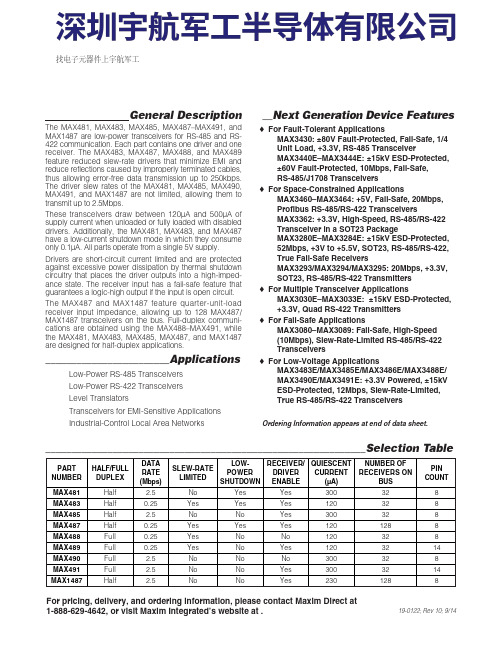
General DescriptionThe MAX481, MAX483, MAX485, MAX487–MAX491, andMAX1487 are low-power transceivers for RS-485 and RS-422 communication. Each part contains one driver and onereceiver. The MAX483, MAX487, MAX488, and MAX489feature reduced slew-rate drivers that minimize E MI andreduce reflections caused by improperly terminated cables,thus allowing error-free data transmission up to 250kbps.The driver slew rates of the MAX481, MAX485, MAX490,MAX491, and MAX1487 are not limited, allowing them totransmit up to 2.5Mbps.These transceivers draw between 120µA and 500µA ofsupply current when unloaded or fully loaded with disableddrivers. Additionally, the MAX481, MAX483, and MAX487have a low-current shutdown mode in which they consumeonly 0.1µA. All parts operate from a single 5V supply.Drivers are short-circuit current limited and are protectedagainst excessive power dissipation by thermal shutdowncircuitry that places the driver outputs into a high-imped-ance state. The receiver input has a fail-safe feature thatguarantees a logic-high output if the input is open circuit.The MAX487 and MAX1487 feature quarter-unit-loadreceiver input impedance, allowing up to 128 MAX487/MAX1487 transceivers on the bus. Full-duplex communi-cations are obtained using the MAX488–MAX491, whilethe MAX481, MAX483, MAX485, MAX487, and MAX1487are designed for half-duplex applications.________________________Applications Low-Power RS-485 Transceivers Low-Power RS-422 Transceivers Level Translators Transceivers for EMI-Sensitive Applications Industrial-Control Local Area Networks__Next Generation Device Features o For Fault-Tolerant Applications MAX3430: ±80V Fault-Protected, Fail-Safe, 1/4Unit Load, +3.3V, RS-485 Transceiver MAX3440E–MAX3444E: ±15kV ESD-Protected,±60V Fault-Protected, 10Mbps, Fail-Safe, RS-485/J1708 Transceivers o For Space-Constrained Applications MAX3460–MAX3464: +5V, Fail-Safe, 20Mbps,Profibus RS-485/RS-422 Transceivers MAX3362: +3.3V, High-Speed, RS-485/RS-422Transceiver in a SOT23 Package MAX3280E–MAX3284E: ±15kV ESD-Protected,52Mbps, +3V to +5.5V, SOT23, RS-485/RS-422,True Fail-Safe Receivers MAX3293/MAX3294/MAX3295: 20Mbps, +3.3V,SOT23, RS-485/RS-422 Transmitters o For Multiple Transceiver Applications MAX3030E–MAX3033E: ±15kV ESD-Protected,+3.3V, Quad RS-422 Transmitters o For Fail-Safe Applications MAX3080–MAX3089: Fail-Safe, High-Speed (10Mbps), Slew-Rate-Limited RS-485/RS-422Transceiverso For Low-Voltage ApplicationsMAX3483E/MAX3485E/MAX3486E/MAX3488E/MAX3490E/MAX3491E: +3.3V Powered, ±15kVESD-Protected, 12Mbps, Slew-Rate-Limited,True RS-485/RS-422 Transceivers For pricing, delivery, and ordering information, please contact Maxim Direct at1-888-629-4642, or visit Maxim Integrated’s website at .______________________________________________________________Selection Table19-0122; Rev 10; 9/14PARTNUMBERHALF/FULL DUPLEX DATA RATE (Mbps) SLEW-RATE LIMITED LOW-POWER SHUTDOWN RECEIVER/DRIVER ENABLE QUIESCENT CURRENT (μA) NUMBER OF RECEIVERS ON BUS PIN COUNT MAX481Half 2.5No Yes Yes 300328MAX483Half 0.25Yes Yes Yes 120328MAX485Half 2.5No No Yes 300328MAX487Half 0.25Yes Yes Yes 1201288MAX488Full 0.25Yes No No 120328MAX489Full 0.25Yes No Yes 1203214MAX490Full 2.5No No No 300328MAX491Full 2.5No No Yes 3003214MAX1487 Half 2.5No No Yes 2301288Ordering Information appears at end of data sheet.找电子元器件上宇航军工MAX481/MAX483/MAX485/MAX487–MAX491/MAX1487Low-Power, Slew-Rate-LimitedRS-485/RS-422 TransceiversPackage Information For the latest package outline information and land patterns, go to . Note that a “+”, “#”, or “-”in the package code indicates RoHS status only. Package drawings may show a different suffix character, but the drawing pertains to the package regardless of RoHS status.16Low-Power, Slew-Rate-Limited RS-485/RS-422 TransceiversMAX481/MAX483/MAX485/MAX487–MAX491/MAX1487Maxim Integrated cannot assume responsibility for use of any circuitry other than circuitry entirely embodied in a Maxim Integrated product. No circuit patent licenses are implied. Maxim Integrated reserves the right to change the circuitry and specifications without notice at any time. The parametric values (min and max limits) shown in the Electrical Characteristics table are guaranteed. Other parametric values quoted in this data sheet are provided for guidance.Maxim Integrated 160 Rio Robles, San Jose, CA 95134 USA 1-408-601-100017©2014 Maxim Integrated Products, Inc.Maxim Integrated and the Maxim Integrated logo are trademarks of Maxim Integrated Products, Inc.。


MH500 IQ Specs●Btu per burner- 515,000●CFM per burner- 3200●Fuel consumption per burner- 3.65 Gal/h●Recommended fuel consumption- K-1 Kerosene or No.1 Diesel●Operating power per burner- ~115 V, 1-PH, 60Hz 24 A (MAX 82 A)●Weight per burner- 357 lbs●Nozzles per burner- 2 GPH 60` Delavan Type A & 1 GPH 60` Delavan Type W ●Operating fuel pressure- 145 PSI/ 1000 kpa/ 10 barOverviewThe IQ system is a design that allows for the simplicity and ease ofoperation. At start up the IQ system will calibrate for the ambient air temperature and elevation to determine the air to fuel ratio setting for theair band. There are no more calibrations needed after this point and the IQsystem will recalculate the airband adjustment as ambient temperaturechanges.Control Screen Flickering/ Turning off & On❏The screen is a 12 volt system and receives power from the transformer box next to the IQ controller. Check power at the two terminal wires (blk & white) going into the right side of the IQ control. Check all connections on the main PC board and fuses.❏Check the Voltage regulator in the control box below Image (A). Make sure all voltage is proper.❏Make sure the rocker switch on the heater outlet door is working (Picture below).The switch is a two pole switch that closes once the door is opened. Power is sent to the screen for illumination.❏❏❏If the problem persists and power at the converter box showing 12 volts to the screen, then replace the screen.Engine Does Not Run**M axi Heat 500IQ will not start ( The engine will crank over ,but not run) Isuzu GensetNote:I f the unit has a shocker valve, check the value and make sure the shocker is open.** ❏Ensure the unit has enough fuel.❏Go through and check all the connections and most importantly check the emergency shutdown connection to make sure the connection is secure.(IsuzuEngine Timer Module-921432/ Cat C1.5 T4F- 650302)❏If all connections are secure then check to see if the engine is getting fuel.❏Pull the return line on the fuel pump and turn the engine over to see if the fuel pump is working correctly. Loosen the injector line at the injector to see if there is further fuel flow.❏The unit is getting fuel and the Fuel pump is working, find the fuel solenoid on the engine. Check the fuel shut off solenoid to ensure plunger retracts (example “A”, solenoid plunger retracts from voltage on hold wire)❏If the pump works when an auxiliary power source is applied then trace through wiring for loss of voltage. Power is pulled from the engine starter and goesthrough the temp and oil pressure switches. Check schematic for further testing.❏Burner Cycles On & Off**Maxi Heat 500IQ has one burner that will begin to run and then shuts down for High Temp Fault. ( Message appears on the IQ screen).**❏Each burner or both cycling on and off indicates that there is a possibility of backpressure. Back pressure occurs when the flow of heat is restricted and notmoved which accumulates at the outlet or in the burner itself. Kinks in the ducting can cause this issue. Make sure the ducting is straight with limited bends and no elevated lifts or descending of the ducting.❏Check ducting for proper flow.❏Ensure the high limit sensor is working at the end of the outlet.❏Check the main blower fans connection and ensure it is turning on as needed.Faulty connections or loss of power can cause a stall in fan operation which inturn causes the heater to increase temperature.❏Make sure heat going into the area is ventilated so heat does not accumulate and raises temperature to increase output.Blower Fan Stops Circulating or gets a Red “X” over fan:**MH 500 IQ has a burner that will start up and the fan will not turn on. Fan not running will cause the unit to shut down.**❏When this fault occurs it is an indication the fan is losing power.❏Check all the circuits to the fan. Power comes from 120 plug in into the bottom of the IQ controller.❏Start with going to the IQ control box for the burner that is having the issue. Open the cover of the box and over to the side is a wrench icon, press it. After pressing the icon type the password 123 then press the Enter button. You can control the fan manually from this point.❏Note: If you turn the fan on manually and the fan doesn't run, then the motor for the fan could be faulty and need to be replaced (#107194) ❏If the fan runs while in manual mode then the fan is working and power going to fan is ok. The circuit into the IQ controller that controls the blower fan has a loose or faulty connection.❏Check the red terminal block at the bottom of the IQ controller (See examples below). 120 volts into the terminal block feeds the relay above it and into the fan circuit during the purge process.No Power To IQ Control**Maxi Heat 500IQ Controller does not turn on or has no power to the IQ box.**❏No power into the IQ controller will not activate the LCD screen for further operation. Make sure the door on the outlet (heat out of burner) side isopen. The micro switch in the corner of the door activates power to eachscreen. * Switch is a two pole switch, if one side fails then the other couldstill open and provide power to the other screen.*❏Check the relay in the transformer box next to the controller (Example “A”). Make sure connections are secure and the relay is functioningproperly.❏Check the heater element on top of the fuel water separator filter. If element shorts then it will draw too much amperage and not allow thescreen to power up.❏If the IQ controller has 12 volts on the two wire ( example “B” below) harnesses into the side of the controller. If the wire has 12 volts then thescreen needs to be replaced.❏Example “A”Example “B”❏Burner shuts off for “Burner Power Break” or will not turn on**Burner shuts off or always seeing “Burner Power Break “ fault on screen.**❏During the purge cycle at the initial start up the burner ignitor box receives all its power from the IQ controller. System is 120 volts and is used topower the burner and fuel system.❏“Power Break” refers to the break in power to the burner. Test for loss of voltage at the Ignitor box in the burner assembly. (See example “B”) ❏Terminal “N” & “L” are power in. If there is no voltage then check the IQ controller for power loss. Power into the controller red terminal blockdistributes voltage to the fan and burner.❏Check the red terminal block for power in and out (120 v). Make sure connections are secure.❏Check the 15 amp fuse on the left of the controller. (Example “C”). If it fails, replace it.❏Test for voltage into the power relay above the red terminal block. During purge power goes to relay and out into the thermal breaker. (Example“C”). If failed, replace it.Example “B”Reset Safety Thermostat fault:**Safety thermostat is a protection for the high limit. If the fan has failed or heater shut down incorrectly it creates trapped heat which trips the thermostat.**❏Look for the black cap on the heat exchanger below the main blower fan.(Example “A”)❏Remove the cap and you will expose a red button. This button isconnected to the safety thermostat and has to be reset. Push and hold forfive seconds.❏If the thermostat continues to trip then give it 5 to 10 minutes for the heat to dissipate.❏If the problem persists then replace the safety thermostat.❏Burner starts to smoke and build black smoke out of exhaust stack:** Black smoke is an indication the unit is not getting enough air, bad fuel or carbon build up in the chamber.**❏Make sure air setting is on a specified number that the IQ controller recommends at the time of start up. D O NOT adjust air setting duringoperation unless the IQ controller specifies. (Any change of ambienttemperature and elevation requires smaller or higher amounts of airmixture.)❏Check for any debris or material covering or blocking the air damper.Clean and clear.❏Check fuel pressure and maintain 140-145 PSI at the pump.❏Ensure fuel nozzle NO 1 & NO 2 are both clean and working correctly.Check the schematic for a list of wiring for each nozzle. IQ logic controlsboth nozzles to maintain temperature.❏Make sure the heat exchanger and burn chamber are clear of any soot build up. If there is a large amount of build up then take the burner apartand wash with hot water high pressure hose. Let the barrel air dry beforeusing.❏Make sure only NO 1 Diesel fuel is used. Any additives can cause more gel-like substances which will create fuel issues.Filters perengine option:MH 500IQ MCS W/ ISUZU T4F 3CE1BurnerFUEL FILTER (35MICRON) 107222 ****MH**\ 14-******EngineAIR FILTER 650290 ****MH**\ 14-****** OIL FILTER 22-000309 ****MH**\ 14-****** FUEL FILTER 22-000310 ****MH**\ 14-******FILTER KIT (ALLFILTERS) 108461 ****MH**\ 14-******MH 500IQ MCS W/ CAT 1.5 NA T4FFUEL FILTER (35MICRON ) 107222 ****MH**\ 14-******EngineAIR FILTER 102580 ****MH**\ 14-****** OIL FILTER 650304 ****MH**\ 14-****** FUEL FILTER 103155 ****MH**\ 14-******FILTER KIT (ALLFILTERS) 108464 ****MH**\ 14-******Oil Change Intervals:Caterpillar C1.5- Every 500 hoursIsuzu 3CE1- Every 500 hoursIsuzu T4F 3CE1 Parts:●Dipstick Tube EXT Assy- ( 100604 )●Starter-102465●AVR Board-103016●Stop Solenoid--22-000316●Stop Solenoid O Ring- 22-000329●Alternator Diode- 22-000324●Temp Switch- 22-000325●Oil Pressure Switch- 22-000326●Relay Assembly- 650423●Fuel Pump- 22-000317●Auto Shutdown Timer-921432●Filter Kit (Air Fuel & Oil)- 108959●Fuel Water Separator ( 35 Micron Fuel Filter)- 107222●Timer Module-921432Cat 1.5 T4F Parts:●Ignition Keys- 920474●Ignition/Cat- 920475●Hour Meter- 340014●Timer/Shutdown- 650302●Cat 1.5 Muffler-104867●Muffler Gasket- 650234● 3 way Fuel Gauge- 103205●Filter Kit (Air Fuel & Oil)- 108961●Fuel Water Separator ( 35 Micron Fuel Filter)- 107222●Timer Shutdown-650302*Check engine operators manual for specific recommended lubricants.*Additional warranty information & claim forms can be obtained on .*Please contact Allmand Tech line for additional help and troubleshooting @ (308)995-3431 / Parts (800) 562-1373.。

Technical DataOriginal InstructionsNon-fused Rotary Disconnect Switch Specifications Bulletin 194UTopic PageSummary of Changes2Catalog Number Explanation3Product Selection3Disconnect Switch Bodies3Disconnect Switch Kits3Switch Handles4Additional Terminals5Other Accessories5Specifications6Approximate Dimensions8Additional Resources13Non-fused Rotary Disconnect Switch Specifications Technical DataSummary of ChangesThis publication contains the following new or updated information. This list includes substantive updates only and is not intended to reflect all changes.Topic PageUpdated fuse information6Corrected short-circuit current rating information labels72Rockwell Automation Publication 194U-TD001D-EN-P - November 2021Rockwell Automation Publication 194U-TD001D-EN-P - November 2021330…160 A Disconnect SwitchesCatalog Number ExplanationExamples that are given in this section are not intended to be used for product selection. Not all combinations generate a valid cat. no. Use ProposalWorks software to configure the 194U Disconnect Switch. ProposalWorks software is available from rok.auto/systemtools .Product Selection194U –A 30–1753abcdabcdBulletin NumberMounting Type Rated Current [A]No. of Poles, OFF-ON 90° Configuration Code DescriptionCode Description Code UL IEC 194UNon-fused disconnect switchA DIN Rail/Base mount 303040Code Description E Front M ount60606317533 Poles10010012517544 Poles (160 A devices only)160125160Disconnect Switch BodiesDescriptionRated Current [A]No. of PolesCat. No.UL IEC Base Mount Disconnect Switch30403194U-A30-17536063194U-A60-1753100125194U-A100-17531251603194U-A160-17534194U-A160-1754Front Mount Disconnect Switch30403194U-E30-17536063194U-E60-1753100125194U-E100-17531251603194U-E160-17534194U-E160-1754Disconnect Switch KitsDescriptionHandle Color Rated Current [A]No. of PolesCat. No.UL IECFront-mounted disconnect switch kit •Contains switch body, handle, and shaftBlack1251603194U-160DMK-3B 4194U-160DMK-4B Red/yellow3194U-160DMK-3Y 4194U-160DMK-4Y4Rockwell Automation Publication 194U-TD001D-EN-P - November 202130…160 A Disconnect Switches AccessoriesAccessoriesSwitch HandlesDescriptionFor Use WithColor Cat. No.Padlockable handle, standard •Type 3R, 3, 12, 4, 4X •IP66Bul. 194U base-mounted switches,30…160 ABlack 194R-PB Red/yellow 194R-PY Padlockable handle, standard •Type 3R, 3, 12, 4, 4X •IP66Bul. 194U base-mounted switches,30 (100)ABlack194E-SBRed/yellow 194E-SYPadlockable handle, standard •Type 3R, 3, 12, 4, 4X •IP66•Requires Cat. No. 194U-DMABul. 194U front-mounted switches,160A Black194U-FB Red/yellow194U-FYNFPA 79 internal operating handle with 12 in. (30.48cm) shaft•Requires 194U-LOTO adapterBul. 194U base-mounted switches, 30…160A with 194R-PB, 194R-PY, 194E-SB, and 194E-SY handles only—194U-N1Switch Handles with Legend PlatesDescriptionLegend Marking Switch CurrentRatingFor Use WithColorCat. No.Type N handle•67 x 67 mm (2-41/64 x 2-41/64 in.)•Locking for up to three padlocks (padlocks not included)•Type 1/12O - I OFF-ON30…100 AFront- and base-mounted switches Red/yellow194L-HE6N-175Type G handle•67 x 67 mm (2-41/64 x 2-41/64 in.)•Locking for up to three padlocks (padlocks not included)•Type 1/12O - I OFF-ON 30…100 AFront- and base-mounted switchesBlack/grey 194L-HE6G-175Type L handle•67 x 67 mm (2-41/64 x 2-41/64 in.)•Locking for one padlock (padlock not included)•Type 1/12O - I 30…100 AFront- and base-mounted switchesRed/yellow 194L-HE6L-175OFF-ON 194L-HE6L-175I Type E handle•67 x 67 mm (2-41/64 x 2-41/64 in.)•Locking for one padlock (padlock not included)•Type 1/12O - I 30…100 AFront- and base-mounted switches Black/grey194L-HE6E-175OFF-ON 194L-HE6E-175I Type I handle•67 x 67 mm (2-41/64 x 2-41/64 in.)•Type 1/12O - I 30…100 AFront- and base-mounted switches Red/yellow194L-HE6I-175OFF-ON 194L-HE6I-175I Type A handle•67 x 67 mm (2-41/64 x 2-41/64 in.)•Type 1/12O - I30…100 AFront- and base-mounted switches Black/grey194L-HE6A-175OFF-ON194L-HE6A-175IRockwell Automation Publication 194U-TD001D-EN-P - November 2021530…160 A Disconnect Switches AccessoriesAdditional TerminalsDescriptionMounting StyleFor Use With Cat. No.Ground terminalBase30, 60 A switches 194U-A60-PE 100 A switches 194U-A100-PE Front/Door 30, 60 A switches 194U-E60-PE 100 A switches 194U-E100-PE 4th pole terminalBase100 A switches (1)(1)May be used with 30…60 A disconnect switch with the wire range of 100 A device.194U-A100-FP Front/Door100 A switches(1)194U-E100-FPOther AccessoriesDescriptionFor Use WithCat. No.Extension kit for G, N, I, A, L, E handles9.25 in. (23.5 cm)Base-mounted 30…100 A switches194U-G339313.9 in. (35.3 cm)194U-G3394Shaft for G, N, I, A, L, E handlesFront-mounted 30…100 A switches 194U-G3688Shaft for 194R-P and 194E-S handles12 in. (30.5 cm)Base-mounted 30…160 A switches194U-S121 in. (53.3 cm)194U-S2Front-mount handle adapter•for use with 194U-F padlockable handles160 A switches 194U-DMA Auxiliary contactN.C.30…160 A switches 194U-NC N.O.194U-NO N.O./N.C.30…100 A switches 194U-NONC Terminal Shroud1-pole (qty: 1)30…100 A switches 194U-C13-pole (qty: 1)30…100 A switches 194U-C3160 A switches 194U-160-C34-pole (qty: 1)160 A switches 194U-160-C4Padlock accessory (1)(1)Required for Cat. No. 194U-N1.base-mounted 30…160 A switches194U-LOTORepair Kit •4 screws for 194L-HE handle•6 bolts for 194U-F handle front mount •metal ring for 194U-LOTObase- and front-mounted 30…160 Aswitches194U-RK30…160 A Disconnect Switches SpecificationsSpecificationsTable 1 - UL Ratings194U-*30 194U-*60 194U-*100 194U-*160 Standards Compliance UL98, cULus UL98, cULus UL98, cULus UL98, cULus UR Ampere rating [A] 30 60 100 100 125 Max Voltage [V AC] 600 600 600 600 600 Max Hp/FLA, 3-phase AC240V [Hp/A] 10/28 20/54 30/80 40/104 40/104 480V [Hp/A] 20/27 40/52 50/65 75/96 75/96 600V [Hp/A] 30/32 30/32 30/32 100/99 100/99 Max Hp/FLA, 1-phase AC120V [Hp/A] 2/24 3/34 5/56 — — 240V [Hp/A] 5/28 7.5/40 15/68 20/88 20/88 480V [Hp/A] — — — 30/66 30/66 Max Hp/FLA, 250V DC [Hp/A] — — — 20/60 20/60 Short Circuit ratingFuse size[A]6060 150/100200200 J fuse[kA] 200 20050/200 100 100 T fuse[kA] 200 20050/200 100 100 Electrical endurance, operating cycles 6000 6000 6000 6000 6000 Mechanical endurance, operating cycles 10000 10000 10000 10000 10000Wire range [mm2] 10...70 10...70 10...70 10...70 10 (70)[AWG] 14…4 14…4 8…1/0 8…1/0 8…1/0Tightening torque[lb•in] 55 55 55 53 53 Table 2 - IEC RatingsIEC Specification 194U-*30 194U-*60 194U-*100 194U-*160 Standards Compliance EAC, IEC EAC, IEC EAC, IEC, CCC EAC, IEC, CCC Rated insulation Voltage/Operational voltage AC20/DC20[V] 750 750 750 1000 Rated impulse withstand voltage[kV] 8 8 8 12Rated operational current, AC-20/DC20Open/Enclosed 35 °C (95 °F)[A] — — — 160 40 °C (104 °F)[A] — — 125 160Enclosed 35 °C (95 °F)[A] — — — 160 40 °C (104 °F)[A] — — 100 —Cu Wire cross section[mm2]——5070 Rated operational current, AC-21A415…690V[A] — — 125 160 Rated operational current, AC-22A415…690V[A] 40 63 125 160 Rated operational current, AC-23A415V[A] 40 63 90 160 440V[A] 40 63 65 —500V[A] 40 63 60 160 690V[A] 40 40 40 160 Rated operational current, DC-21A1 pole in series 24…48V[A] — — 125 —2 poles in series 110V[A] — — 125 —4 poles in series 220V[A] — — 125 —6Rockwell Automation Publication 194U-TD001D-EN-P - November 2021Rockwell Automation Publication 194U-TD001D-EN-P - November 2021730…160 A Disconnect Switches SpecificationsRated operational current, DC-22A 1 pole in series 24…48V [A] — — 125 —2 poles in series 110V [A] — — 125 —4 poles in series220V [A] — — 80 — Rated operational current, DC-23A 1 pole in series 24…48V [A] — — 125 —2 poles in series 110V [A] — — 125 —4 poles in series220V[A] — — 63 — Rated operational power, AC-23A 220…240V [kW] — — 22 45400…415V [kW] 15 18.5 45 75440V [kW] — — 45 75500V [kW] — — 45 90690V[kW] 15 15 45 132 Rated breaking capacity, AC-23A 415V [A] — — 720 1280440V [A] — — 624 1280500V [A] 184 360 560 1280690V[A] 96 160 400 1280 Rated breaking capacity, DC-23A 24…48V [A] — — 500 —110V [A] — — 500 —220V[A]128180252—Rated conditional SCCR, I q (r.m.s) (1)I q (r.m.s) 50 kA [kA] 16.5 16.5 16.5 —Max fuse size gG/aM up to 415V [A] 125/125 125/125 125/125 —I q (r.m.s)100 kA [kA] — — — 30 Max fuse size gG/aM 500V [A] — — — 200/200I q (r.m.s) 10 kA [kA] 8.2 8.2 8.2 —Max fuse size gG/aM 690V [A] 125/100 125/100 125/100 —I q (r.m.s)50 kA [kA] 10 10 10 24Max fuse size gG/aM690V [A] 63/63 63/63 63/63 200/200 Rated short-time withstand current r.m.s690V, 1 s [kA] 2.5 2.5 2.5 4690V, 0.25 s [kA] — — —7 Peak690V/500V[kA] 3.6/3.6 3.6/3.6 3.6/3.6 12/— Power lost per pole[W] 0.7 1.6 6.3 6.5 Weight[kg]0.4 0.4 0.44 0.9 (3-pole)1.1 (4-pole)[lb]0.880.880.971.98 (3-pole)2.42 (4-pole)Operating temperature [ °C] -5...+40 -5...+40 -5...+40 -5...+40[ °F]23...10423...10423...10423 (104)Storage temperature[ °C] -25…+55 -25…+55 -25…+55 -25…+55[ °F]-13...131-13...131-13...131-13 (131)(1)Rated conditional short-circuit current I q (r.m.s.) and corresponding maximum allowed let-through current I c of fuse. The let-through current I c refers to values listed by fusemanufacturers (single phase test according to IEC60269)Table 2 - IEC Ratings (Continued)IEC Specification194U-*30194U-*60 194U-*100 194U-*1608Rockwell Automation Publication 194U-TD001D-EN-P - November 202130…160 A Disconnect Switches Approximate DimensionsApproximate DimensionsDimensions are in millimeters (inches). Dimensions are not intended to be used for manufacturing purposes.Figure 1 - 30, 60, and 100 A Base-mounted Switches, 3-pole DevicesFigure 2 - 30, 60, and 100 A Door-mounted Switches, 3- and 4-pole Devices100 (3.93)100 (3.93)8.8 (0.35)56(2.20)73(2.87)63(2.48)46 (1.81)90 (3.54)56.5(2.22)70(2.76)dia 4.5(0.18)0°90°180°270°Mounting PositionMinimum enclosure size for 30…100 A switches is 204 x 153 x 102 mm (8.0 x 6.0 x 4.0 in.)100 (3.94)67(2.64)70(2.76)56 (2.20)48 (1.89)45(1.77)21.5(0.85)80 (3.15)50 (1.97)35(1.38)29.2(1.15)19.2(0.76)17.7(0.7)13(0.51)6.3(0.25)19.3(0.75)22.3(0.88)14(0.55)13.1(0.52)1(0.04)56(2.20)48(1.89)0°90°180°270°Mounting PositionMinimum enclosure size for 30…100 A switches is 204 x 153 x 102 mm (8.0 x 6.0 x 4.0 in.)Rockwell Automation Publication 194U-TD001D-EN-P - November 2021930…160 A Disconnect Switches Approximate DimensionsFigure 3 - 160 A Base-mounted Switches, 3-pole Devices123(4.84)73.1(2.88)61.6(2.43)23(0.91)36(1.42)26.6(1.05)130 (5.12)46 (1.81)42 (1.65)27(1.06)54(2.13)19.5(0.77)103.5(4.07)52.5(2.07)80.1 (3.15)65 (2.56)22.4(0.88)11.54(0.45)R3.4(0.13)R4.5(0.18)R6(0.24)12 (0.47)42.3(1.67)10.2(0.4)9.1(0.36)37.2(1.46)47(1.85)17.7(0.69)4.4(0.17)2.6(0.10)42(1.65)130 (5.12)72(2.83)122 (4.8)0°90°180°270°dia 4.5(0.18)Mounting PositionMinimum enclosure size is 400 x 600 x 230 mm (15.76 x 23.64 x 9.06 in.)10Rockwell Automation Publication 194U-TD001D-EN-P - November 202130…160 A Disconnect Switches Approximate DimensionsFigure 4 - 160 A Base-mounted Switches, 4-pole DevicesFigure 5 - 160 A Door-mounted Switches, 3-pole Devices150 (5.91)33.7(1.33)42(1.65)37(1.46)130.5 (5.14)55.5(2.19)40.1(1.58)37(1.46)11.6(0.46)60.4(2.38)113 (4.45)24(0.94)3 (0.12)42.3(1.67)36.6 (1.44)22.4(0.88)7.1(0.28)52.5(2.07)130(5.12)12(0.47)27(1.06)80.1(3.15)0°90°180°270°99 (3.9)dia 4.5(0.18)122(4.8)Mounting Position73(2.87)138 (5.43)65(2.56)43.5(1.71)34.4(1.35)16.5 (0.65)27(1.06)67.9 (2.67)12.1(0.48)56(2.20)80.1(3.15)123(4.84)46(1.81)27.5(1.08)123 (4.84)92.1 (3.63)13(0.51)60.4(2.38)46.3(1.82)42.3(1.67)82.7 (3.26)45.1(1.78)R21.3(0.84)R8(0.31)R6 (0.24)R3.4 (0.13)130.5 (5.14)0°90°180°270°Mounting PositionRockwell Automation Publication 194U-TD001D-EN-P - November 20211130…160 A Disconnect Switches Approximate DimensionsFigure 6 - 160 A Door-mounted Switches, 4-pole Devices130 (5.12)165(6.49)65 (2.56)55.03 (2.17)45 (1.77)82.9 (3.26)60 (2.36)52(2.05)53.5(2.11)13(0.51)23.3(0.92)17.5(0.69)3(0.12)27.5(1.08)13.5(0.53)55(2.17)8.2 (0.32)60.4(2.38)92.2 (3.63)29.7(1.17)17.694.4(0.17)27(1.06)21.6(0.85)81(3.19)148.9(5.86)110 (4.33)87.9 (3.46)Ø 6.8(0.27)Ø 12(0.47)Ø 16(0.63)Ø 42.6(1.68)73(2.87)56 (2.20)0°90°180°270°Mounting Position30…160 A Disconnect Switches Approximate DimensionsNotes:12Rockwell Automation Publication 194U-TD001D-EN-P - November 2021Rockwell Automation Publication 194U-TD001D-EN-P - November 202113Non-fused Rotary Disconnect Switch Specifications Technical DataAdditional ResourcesThese documents contain additional information concerning related products from Rockwell Automation.You can view or download publications at rok.auto/literature .ResourceDescriptionUL Standards Listing for Industrial Control Products, publication CMPNTS-SR002Assists original equipment manufacturers (OEMs) with construction of panels, to help ensure that they conform to the requirements of Underwriters Laboratories.American Standards, Configurations, and Ratings: Introduction to Motor Circuit Design, publication IC-AT001Provides an overview of American motor circuit design based on methods that are outlined in the NEC.Industrial Components Preventive Maintenance, Enclosures, and Contact Ratings Specifications, publication IC-TD002Provides a quick reference tool for Allen-Bradley industrial automation controls and assemblies.Safety Guidelines for the Application, Installation, and Maintenance ofSolid-state Control, publication SGI-1.1Designed to harmonize with NEMA Standards Publication No. ICS 1.1-1987 and providesgeneral guidelines for the application, installation, and maintenance of solid-state control in the form of individual devices or packaged assemblies incorporating solid-state components.Industrial Automation Wiring and Grounding Guidelines, publication 1770-4.1Provides general guidelines for installing a Rockwell Automation industrial system.Product Certifications website, rok.auto/certifications .Provides declarations of conformity, certificates, and other certification details.Publication 194U-TD001D-EN-P - November 2021Supersedes Publication 194U-TD001C-EN-P - June 2019Copyright © 2021 Rockwell Automation, Inc. All rights reserved. Printed in the U.S.A.Rockwell Automation SupportUse these resources to access support information.Documentation FeedbackYour comments help us serve your documentation needs better. If you have any suggestions on how to improve our content, complete the form at rok.auto/docfeedback .Technical Support Center Find help with how-to videos, FAQs, chat, user forums, and product notification updates.rok.auto/supportKnowledgebaseAccess Knowledgebase articles.rok.auto/knowledgebase Local Technical Support Phone Numbers Locate the telephone number for your country.rok.auto/phonesupport Literature LibraryFind installation instructions, manuals, brochures, and technical data publications.rok.auto/literature Product Compatibility and Download Center (PCDC)Download firmware, associated files (such as AOP, EDS, and DTM), and access product release notes.rok.auto/pcdcRockwell Automation maintains current product environmental compliance information on its website at rok.auto/pec .Allen-Bradley, expanding human possibility, and Rockwell Automation are trademarks of Rockwell Automation, Inc.EtherNet/IP is a trademark of ODVA, Inc.Trademarks not belonging to Rockwell Automation are property of their respective companies.Rockwell Otomasyon Ticaret A.Ş. Kar Plaza İş Merkezi E Blok Kat:6 34752, İçerenköy, İstanbul, Tel: +90 (216) 5698400 EEE Yönetmeliğine Uygundur。

Goodman Manufacturing Company, L.P .5151 San Felipe, Suite 500, Houston, TX 77056© 2004, 2007, 2009 - 2011, 2014 - 2015 Goodman Manufacturing Company, L.P.USER’S INFORMATION MANUALP ACKAGE G AS -E LECTRICInstaller -Affix this manual, Installation Guide, and Warranty adjacent to the appliance.Owner -Read and keep all product literature in a safe place for future reference.RECOGNIZE THIS SYMBOL AS A SAFETY PRECAUTION.HI-116E 7/152S IGNAL W ORDSDear Homeowner, please recognize the following safety infor-mation. This information will alert you to the potential for per-sonal injury.- Indicate hazards or unsafe practices which result in severe personal injury or death.Before using this manual, check the serial plate for propermodel identification.The installation and servicing of this equipment must be performed by qualified, experienced technicians only.G ENERAL I NFORMATIONU NIT L OCATIONThis unit is approved only for an outdoor installation. See the installation instructions for the required clearances to the unit. It is important that safety measures are taken in the surrounding area of the unit.Gutters or deflectors must be installed on the roof to prevent water from shedding on the unit.1.An area must be available to reach the unit in a clear and unobstructed path.2.The unit area and the vicinity of any other gas appliances must be kept clear and free of combustible materials, gaso-line, and other flammable vapors and liquids. Also, do not store or use flammable items such as paint, varnish, or lac-quer in the area.3.The combustion air supply must not be contaminated by prod-ucts containing chlorine or fluorine, as they could corrode the heat exchanger. If you need further information on this sub-ject, contact your installing dealer or another qualified ser-vicer.4.Familiarize yourself with the controls that turn off the gas and electrical power to the unit.5.Establish a regular service and maintenance schedule to ensure efficient and safe operation of the unit.6.The unit must be placed where no runoff water from higher ground can collect in the unit.U NIT I NSTALLATIONExamine the unit installation to determine the following:1.The flue hood connector is in place and is physically sound without holes or excessive corrosion.2.The mounting pad support of the unit is sound.3.There are no obvious signs of deterioration of the unit.4.The burner flames are stable, soft and blue, (dust may cause orange tips but must not be yellow). The flames should ex-tend directly outward from the burner without curling, floating,or lifting off. To examine, turn on the electrical power and gas.Set the room temperature to the maximum setting.BurnerNOTE: If a strong wind is blowing, it may not be possible to perform the flame inspection.A IR REQUIREMENTSSince the gas/electric unit is installed completely in the outdoors, the depletion of combustion air is highly improbable. To ensure an adequate supply of combustion air, do not allow the combus-tion air inlet or the flue hood outlet to become blocked by leaves, snow, rubbish, or insect (wasps) nests. Never block the con-densing unit section in the winter with covers. Blocking of this section would prevent an adequate amount of combustion air from reaching the furnace section.Great care has been taken in the design and manufacture of your unit to provide for your comfort and safety. Be aware of the possibility that some problems with your unit or other gas-fired appliances could cause flue gases to be present in your building. These flue gases could include carbon monoxide.3T HERMOSTA TThis unit will not operate properly without a good quality, correctly installed thermostat. It is very important that the thermostat be located where it can best “sense” the average room temperature. Be sure the thermostat is not exposed to hot or cold drafts or to hot or cold spots on the wall, such as those received from outside walls, walls with pipes inside, or from openings into the attic. No matter the type or style, thermostat operation is basically the same. The most widely used types will control both heating and cooling functions and will have a Fan Switch with Auto and ON settings. On Auto, the Circulating Air Blower will cycle on/off, but if switched to ON it will run constantly.For Dual Fuel units (GPD/APD), a Dual Fuel thermostat with an outdoor temperature sensor is recommended for optimal opera-tion.IMPORTANT NOTE: To avoid the possibility of damage to the unit heat exchanger, do not set the thermostat fan switch to ON (constant fan operation) during the heating season without first consulting the installer of the unit or another qualified servicer. There are thermostats that automatically switch from Heating to Cooling, or with night setbacks. The night setback, or multiple setback type, will lower the temperature at night or during the day when the building is unoccupied.Propane (LP) Gas Installations OnlyFor units operating on propane gas, please review the following warnings before use.O PERATING INSTRUCTIONSH EATING S TART U PTo put your unit into operation, follow the steps listed below.1.Close the external manual gas shutoff valve.2.Turn off the electrical power to the unit.3.Set the room thermostat to the lowest possible setting.4.Remove the heat exchanger door on the side of the unit byremoving screws.5.This unit is equipped with an ignition device which automati-cally lights the burner. Do not try to light the burner by hand.6.Move the gas control switch to the OFF position. Do not useexcessive force.7.Wait five minutes to clear out any gas. Then smell for gas,including near the floor as some types of gas are heavier than air.8.If you smell gas following the five minute waiting period instep 7, immediately follow the instructions on the cover of this manual. If you do not smell gas after five minutes, move or rotate the gas control switch to the ON position. The switch should turn easily. Do not use excessive force.9.Reinstall the burner compartment door.10.Open the external manual gas shutoff valve.11.Turn on the electrical power to the unit.12.Adjust the thermostat to a setting above room temperature.13.After the burners are lit, set the thermostat to desired tem-perature.H EATING S HUT D OWNTo shut down operation, follow the steps listed below.1.Set the thermostat to the lowest setting.2.Turn OFF electrical power to the unit.3.Remove the heat exchanger door on the side of the unit byremoving screws.4.Move the gas control switch to the OFF position. Do not useexcessive force.5.Close the external manual gas shutoff valve.6.Reinstall the heat exchanger door.7.If cooling and/or air circulation is desired, turn ON the electri-cal power.C OOLING O PERATIONCooling operation may be obtained as follows:1.Place the room thermostat selector switch in the COOL po-sition (or AUTO, if available, and if automatic changeover from cooling to heating is desired).2.Set the room thermostat to the desired temperature.3.If cooling system does not energize, wait five minutes. Thesystem startup may be delayed by the short-cycle protector feature of the ignition control board. Check the manual reset devices on the rollout limit, as described in this manual.OUTLET Gas ValveOn/OffSelectorSwitchWhite-Rodgers Model 36F224SelectorSwitchINLET OUTLETWhite-Rodgers Model 36G22High RegulatorWhite-Rodgers Model 36G54Honeywell Model VR8215 (Single-Stage)S AFETY C IRCUITSA number of safety circuits are employed to ensure safe and proper unit operation. These circuits serve to control any poten-tial safety hazards and, as inputs in the monitoring and diagnosis of abnormal operation.S ECONDARY L IMITThe secondary limit control is located on the blower housing and monitors blower compartment temperatures. It is a normally closed (electrically), automatic reset, temperature activated sensor. This limit guards against overheating as a result of insufficient conditioned air passing over the heat exchanger. It deenergizes the gas valve if the blower fails.NOTE: If the power to the unit is interrupted during the heating cycle, it may cause the secondary limit to trip. Once the blower compartment temperature drops below the limit reset temperature, the limit will automatically reset.Secondary Limit ControlR OLLOUT L IMITThe rollout limit is a normally-closed (electrically), manual-reset, temperature-activated sensor. It is mounted on the burnerbracket and monitors the burner flame. If there is an improper draw of burner flames into the heat exchanger, the rollout limit will detect it and shut off gas flowing to the burners. Contact a qualified servicer to check the unit before resetting this device.Rollout Protection on Burner Bracket56C OMPRESSOR P ROTECTIOND EVICESThis gas/electric package unit includes components which are designed to protect the compressor against abnormal operat-ing conditions.NOTE: The operation of the indoor blower will not be affected by any compressor protection devices.If, during a call for cooling, the indoor fan runs and circulates room temperature air while the compressor and outdoor fan do not operate:1.Wait five minutes, as a protection device may be holding the compressor off.2.Check the room thermostat to see if it is correctly set.3.If the room thermostat is correctly set, call a qualified servicer to determine if one of the compressor protection devices has opened.S HORT -C YCLE P ROTECTORA short-cycle protector is built into the ignition control. Each time the compressor is off for less than 3 minutes, the short-cycle protector will delay compressor startup for up to 3 minutes. This protects the compressor from improper operation.On Dual Fuel units (GPD/APD), the short-cycle protector will delay the compressor 5 minutes.NOTE: These units are not designed to provide mechanical cooling at outdoor temperatures below 50°F. If low ambient cooling is needed, consult a qualified servicer.I GNITERThe unit has an electronic ignition device which lights the burners automatically. Never try to light the burners by hand. It also has an induced draft blower to exhaust combustion prod-ucts.I NDOOR A IR C IRCULATOR B LOWERKeep the blower access door panel in place except for inspec-tion and maintenance.R OUTINE M AINTENANCEIf you perform maintenance on the unit yourself, remember that certain mechanical and electrical knowledge, skills and tools are required to perform unit maintenance. Personal injury or death may result If you are not properly trained. You should call your installing dealer or place of purchase if you are uncertainabout your ability to perform maintenance.A NNUAL I NSPECTIONYour package unit should be inspected by a qualified installer,or service agency at least twice every year. This check should be performed before the heating and cooling seasons begin. This will ensure that adequate combustion air is being drawn and the vent system is working properly. Particular attention should be paid to the following items. Repair as necessary.•Check physical support of the unit. Ensure it is sound with-out any sagging, cracks, or gaps, around the base.•Check for obvious signs of deterioration of the unit.•Flue Hood and Combustion Air Inlet. Check for blockage (wasp nest, etc.) and corrosion.Flue Hood•Return Air Connection. Check for physical soundness and ensure that the connection is firmly sealed to the package unit casing.•Heat exchanger. Check for corrosion and/or obstructions within the heat exchanger passageways.•Burners. Check for proper ignition, burner flame, and flame sense.•Wiring. Check electrical connections for tightness and/or corrosion. Check wires for damage.•Filters. Check that filters are clean and in the proper place-ment in the unit or duct system.•Louvers. Inspect air inlet louvers inside the heat exchanger compartments. Ensure the area is clean and free of dirt and debris.R EPLACING OR C LEANING F ILTERIMPORTANT NOTE: Never operate unit without a filter installed as dust and lint will build up on internal parts resulting in loss of efficiency, equipment damage and possible fire.A return air filter is not supplied with this unit; however, there must be a means of filtering the return air. The filter(s) may be located in the return air duct(s). Consult with your installing dealer for the actual location of the return air filter(s) in your unit.A dirty filter is the most common cause of inadequate heating or cooling performance. Filter inspection should be made at least every two months; more often if necessary because of local conditions and usage.Dirty throwaway filters should be discarded and replaced with a new, clean filter. Dirty permanent filters should be washed with water, thoroughly dried and sprayed with a filter adhesive before being reinstalled. (Filter adhesives may be found at many hard-ware stores.) Permanent filters should last several years. How-ever, should one become worn or uncleanable, it should be replaced.When installing a new filter or reinstalling an old one, always make certain the air flow arrows on the filter point in the proper direction.C LEAN O UTSIDE C OIL (Q UALIFIED S ERVICER O NLY)The coil with the outside air flowing over it should be inspected annually and cleaned as frequently as necessary to keep the finned areas free of leaves, grass, seeds, and debris.C ONDENSER, E VAPORATOR, AND I NDUCED D RAFT M OTORS Bearings on the air circulating blower motor, condenser motor and the combustion fan motor are permanently lubricated. No additional oiling is required.C OMPRESSORThe compressor motor is hermetically sealed and does not require additional oiling.S AFETY L ABELSNOTE: If safety labels are missing or illegible, contact the installing dealer.To obtain the proper safety labels, the Model and Serial Number of the unit must be supplied. These numbers are recorded on the nameplate of the unit. For convenience, record this information here:MODEL NUMBER:_____________________________________SERIAL NUMBER:_____________________________________78S AFETY L ABELSF OR A DDITIONAL I NFORMATIONMost questions can be answered by your local dealer. If you have other matters that cannot be resolved locally,or you need additional information regarding other heating and cooling products offered by us - please call:CONSUMER INFORMA TION LINE:TOLL FREE1-877-254-4729 (U.S. only)emailusat:******************************fax us at: (731) 856-1821(Not a technical assistance line for dealers.)________________Outside the U.S., call 1-713-861-2500.(Not a technical assistance line for dealers.)Your telephone company will bill you for the call.SAFETY LABELS9SAFETY LABELS10SAFETY LABELS11Goodman Manufacturing Company, L.P. 5151 San Felipe, Suite 500, Houston, TX 77056 12。

SPECIFICATIONS13Models 7520DT, 7530DT, 7540DT, 7550DT and 7564SAFunctional SpecificationsINPUTVoltage 115/230 VAC 15, Single Phase, User selection Frequency 50/60 Hz 5Fuse6.3 Amp 250V Slo-Blo for 7550DT and 7564SA 5 Amp 250V Slo-Blo for 75/20/30/40DTDIELECTRIC WITHSTAND TEST MODEOutput Rating5 KV @ 40 mA for 7550DT and 7564SA, 5 KV @ 20mA for 75/20/30/40DT6 KV @ 10 mA DC for 75/30/40/50DT and 7564SAOutput AdjustmentRange:0 - 5 KV AC 0 - 6 KV DCResolution: 1 volt/step Accuracy:(2 of setting 5 volts) Ramp-HI 12mA peak maximum, ON/OFF selectableCharge-LORange:0.0 - 350.0A DC or Auto setHI-Limit AC Range:0.00 - 40.00 mA for 7550DT and 7564SA, 0.00 - 20.00 mA for 75/20/30/40DT Resolution: 0.01 mA/step Accuracy: (2 of setting 2 counts) DC Range:0 - 9999AResolution: 1A/stepAccuracy:(2 of setting 2 counts) LO-Limit AC Range:0.000 - 9.999 mA Resolution: 0.001 mA/stepAccuracy: (2 of setting 2 counts) DC Range:0.0 - 999.9 AResolution: 0.1A/stepAccuracy:(2 of setting 2 counts) Arc Detection Range:1 - 9Failure DetectorAudible and VisualRecycledEquipment(410)email:***************************1981SPECIFICATIONS14Voltage Display Range: 0.00 - 6.00 KV Full Scale0.00 - 5.00 KV Full Scale for 7520DT onlyResolution: 10 volt/stepAccuracy: (2 of reading 2 counts)Current Display Auto RangeAC Range 1: 0.000mA - 3.500mAResolution: 0.001mA/stepRange 2: 3.00 - 40.00 mA for 7550DT and 7564SA,3.00 - 20.00 mA for 75/20/30/40DTResolution: 0.01 mA/stepDC Range 1: 0.0 A - 350.0 AResolution: 0.1A/stepRange 2: 300 A - 3500 AResolution: 1A/stepRange 3: 3000 A - 9990 AResolution: 10A/stepAccuracy: All Ranges (2 of reading 2 counts)DC Output Ripple 4**********************,ResistiveLoad Discharge Time 200 msMaximum CapacitiveLoad DC Mode1uF < 1KV0.75uF < 2KV0.5uF < 3KV0.08uF < 4KV0.04uF < 5KV0.01uF < 6KVAC Output Wave Form Sine Wave, Crest Factor = 1.3 - 1.5Output Frequency Range: 60 or 50 Hz, User SelectionAccuracy: 1%Output Regulation (1 of setting 5 volts) from no load to full load Dwell Timer Range: 0, 0.3 - 999.9 sec (0 = Constant)Resolution: 0.1 sec incrementsAccuracy: (0.1% + 0.05 sec)Ramp Timer Range: AC 0.1 - 999.9 secDC 0.4 - 999.9 secResolution: 0.1 sec incrementsAccuracy: (0.1% + 0.05 sec)RecycledEquipment(410)email:***************************SPECIFICATIONS15Ground Continuity For 75/20/30/40/50DT Current : DC 0.1 A 0.01A, fixedMax. ground resistance : 1 0.1, fixed Ground Fault Interrupt GFI Trip Current: HV Shut Down Speed: 450 A max (AC or DC)< 1msINSULATION RESISTANCE TEST MODE Model 75/30/40/50DT, 7564SAOutput VoltageRange:100 - 1000 Volts DC Resolution: 1 volt/step Accuracy:(2 of reading 2 volts) Short Circuit Current Maximum: 12mA peak Voltage DisplayRange: 0 - 1000 VResolution: 1 volt/stepAccuracy:(2 of reading 2 counts) Resistance DisplayRange: 1 - 9999 M (4 Digit, Auto Ranging)Resolution:500VDC 1000VDC M M M 0.001 1.000 - 5.388 1.000 - 9.999 0.01 1.40 - 53.88 2.80 - 99.99 0.1 14.0 - 538.8 28.0 - 999.9 1104 - 9999280 - 9999Accuracy:(2 of reading 2 counts) at test voltage 500 - 1000V and 1 - 1000 M(8 of reading 2 counts) at test voltage 500 - 1000V and 1000 - 9999 M(8 of reading 2 counts) at test voltage 100 - 500V and 0 - 1000 MCharge-LO Range: 0.000 - 3.500A or Auto Set HI-Limit Range: 0 - 9999 M (0 = Off) LO-Limit Range: 1 - 9999 MDelay TimerRange: 0, 0.5 - 999.9 sec (0 = Constant) Resolution: 0.1 sec/stepAccuracy:(0.1% + 0.05 sec)Ground Fault InterruptGFI Trip Current:HV Shut Down Speed:450 A max (AC or DC) < 1msRecycledEquipment(410)email:***************************SPECIFICATIONS16GROUND BOND TEST MODE Model 7564SA onlyOutput Voltage Range: 3.00 - 8.00 Volts AC (Open Circuit Limit) Resolution: 0.01 volt/stepAccuracy: (2 % of Setting + 0.03V ) O.C. Condition Output Frequency Range: 60 or 50 Hz, User Selection Accuracy: 1%Output CurrentRange: 3.00 - 30.00 Amps AC Resolution: 0.01 Amp/stepAccuracy :(2 % of Setting + 0.02 A) Current DisplayRange: 0.00 - 30.00 Amps Resolution: 0.01 Amp/stepAccuracy:(3 % of Reading + 0.03 A) Resistance DisplayRange: 0 - 600 m Resolution: 1 m /stepAccuracy:(2 % of Reading + 2 m ) HI-LimitRange: 0 - 600 m for 3 - 10 A 0 - 150 m for 3 - 30 A Resolution: 1 m /stepAccuracy:(2 % of Setting + 2 m ) LO-LimitRange: 0 - 600 m for 3 - 10 A 0 - 150 m for 3 - 30 A Resolution: 1 m /stepAccuracy:(2 % of Setting + 2 m ) Dwell TimerRange: 0, 0.5 - 999.9 sec (0 = Constant) Resolution: 0.1 sec/step Accuracy:(0.1% + 0.05 sec)Milliohm OffsetMax. Offset Capability: 200 mResolution: 1 m / stepAccuracy:(2 % of Setting + 2 m )RecycledEquipment(410)email:***************************SPECIFICATIONS17GENERAL SPECIFICATIONSPLC Remote Control Input - Test, Reset, Recall memory 1, 2 and 3Output - Pass, Fail, Test-in-ProcessMemory Allows storage of up to 50 groups different test programsand 8 step/each memory. Step is not available on 7520DT SecurityProgrammable password lockout capability to avoid unauthorized access to test set-up program. LCD Contrast Setting 9 ranges set by the numeric keys on the front panel. Buzzer Volume Setting 10 ranges set by the numeric key on the front panel.Calibration Software and adjustments are made through front panel. Mechanical Bench or rack mount with tilt up front feet. Dimension7540DT, 7550DT and 7564SA:(W x H x D) 17 x 5.8 x 20.3 in. (432 x 147 x 515 mm) 7520DT and 7530DT:(W x H x D) 17 x 5.8 x 12 in. (432 x 147 x 305 mm)Weight7564SA without scanner 52.5 lbs (24 Kgs) 7564SA with built-in scanner 57.0 lbs (26 Kgs) 7550DT without scanner 50.5 lbs (23 Kgs) 7550DT with built-in scanner 55.0 lbs(25 Kgs) 7540DT with 4 port scanner 39.6 lbs (18 Kgs) 7540DT with 8 port scanner41.8 lbs(19 Kgs) 7530DT scanner not available 24.8 lbs (11.27 Kgs) 7520DT scanner not available 24.8 lbs(11.27 Kgs)Scanner Port Two Port Maximum including the built-in scanner. Not available on 7520DT, 7530DT and 7540DT.Scanner Built-in OptionHigh Voltage x 4 Ports (7540DT only)High Voltage x 8 Ports (75/40/50DT and 7564SA) Ground Bond x 8 Ports (7564SA only)RecycledEquipment(410)email:***************************。


用于Peltier模块的集成温度控制器概论MAX1978 / MAX1979是用于Peltier热电冷却器(TEC)模块的最小, 最安全, 最精确完整的单芯片温度控制器。
片上功率FET和热控制环路电路可最大限度地减少外部元件, 同时保持高效率。
可选择的500kHz / 1MHz开关频率和独特的纹波消除方案可优化元件尺寸和效率, 同时降低噪声。
内部MOSFET的开关速度经过优化, 可降低噪声和EMI。
超低漂移斩波放大器可保持±0.001°C的温度稳定性。
直接控制输出电流而不是电压, 以消除电流浪涌。
独立的加热和冷却电流和电压限制提供最高水平的TEC保护。
MAX1978采用单电源供电, 通过在两个同步降压调节器的输出之间偏置TEC, 提供双极性±3A输出。
真正的双极性操作控制温度, 在低负载电流下没有“死区”或其他非线性。
当设定点非常接近自然操作点时, 控制系统不会捕获, 其中仅需要少量的加热或冷却。
模拟控制信号精确设置TEC 电流。
MAX1979提供高达6A的单极性输出。
提供斩波稳定的仪表放大器和高精度积分放大器, 以创建比例积分(PI)或比例积分微分(PID)控制器。
仪表放大器可以连接外部NTC或PTC热敏电阻, 热电偶或半导体温度传感器。
提供模拟输出以监控TEC温度和电流。
此外, 单独的过热和欠温输出表明当TEC温度超出范围时。
片上电压基准为热敏电阻桥提供偏置。
MAX1978 / MAX1979采用薄型48引脚薄型QFN-EP 封装, 工作在-40°C至+ 85°C温度范围。
采用外露金属焊盘的耐热增强型QFN-EP封装可最大限度地降低工作结温。
评估套件可用于加速设计。
应用光纤激光模块典型工作电路出现在数据手册的最后。
WDM, DWDM激光二极管温度控制光纤网络设备EDFA光放大器电信光纤接口ATE特征♦尺寸最小, 最安全, 最精确完整的单芯片控制器♦片上功率MOSFET-无外部FET♦电路占用面积<0.93in2♦回路高度<3mm♦温度稳定性为0.001°C♦集成精密积分器和斩波稳定运算放大器♦精确, 独立的加热和冷却电流限制♦通过直接控制TEC电流消除浪涌♦可调节差分TEC电压限制♦低纹波和低噪声设计♦TEC电流监视器♦温度监控器♦过温和欠温警报♦双极性±3A输出电流(MAX1978)♦单极性+ 6A输出电流(MAX1979)订购信息* EP =裸焊盘。

P/N: 1802051030011 *1802051030011*MGate 5103Quick Installation GuideEdition 1.2, March 2019Technical Support Contact Information/supportMoxa Americas:Toll-free: 1-888-669-2872 Tel: 1-714-528-6777 Fax: 1-714-528-6778 Moxa China (Shanghai office): Toll-free: 800-820-5036 Tel: +86-21-5258-9955 Fax: +86-21-5258-5505 Moxa Europe:Tel: +49-89-3 70 03 99-0 Fax: +49-89-3 70 03 99-99 Moxa Asia-Pacific:Tel: +886-2-8919-1230 Fax: +886-2-8919-1231 Moxa India:Tel: +91-80-4172-9088 Fax: +91-80-4132-10452019 Moxa Inc. All rights reserved.OverviewThe MGate 5103 is an industrial Ethernet gateway for ModbusRTU/ASCII/TCP, EtherNet/IP, and PROFINET network communications. Package ChecklistBefore installing the MGate 5103, verify that the package contains the following items:• 1 MGate 5103 gateway• 1 serial cable: CBL-RJ45F9-150•Quick installation guide (printed)•Warranty cardPlease notify your sales representative if any of the above items is missing or damaged.Optional Accessories (can be purchased separately)•CBL-F9M9-150: DB9-female-to-DB9-male serial cable, 150 cm •CBL-F9M9-20: DB9-female-to-DB9-male serial cable, 20 cm •CBL-RJ45SF9-150: RJ45-to-DB9-female shielded serial cable, 150 cm•ADP-RJ458P-DB9F: DB9-female-to-RJ45 connector•ADP-RJ458P-DB9F-ABC01: DB9-female-to-RJ45 connector •Mini DB9F-to-TB: DB9-female-to-terminal-block connectorHardware IntroductionLED IndicatorsLED Color DescriptionReady Off Power is off or a fault condition existsGreen Steady: Power is on, and the MGate isfunctioning normallyRed Steady: Power is on, and the MGate is bootingupBlinking slowly: Indicates an IP conflict, or theDHCP or BOOTP server is not respondingproperlyFlashing quickly: the microSD card failedMB/EIP Off Modbus: No communication with ModbusdeviceEtherNet/IP: No I/O data exchangeGreen (Blinking) Modbus: Communication in progress EtherNet/IP: I/O data is exchangingRed (Blinking) Communication errorWhen MGate 5103 acts as ModbusClient/Master:1. Slave device returned an error (exception)2. Received a frame error (parity error, checksum error)3. Timeout (slave device is not responding or TCP connection timed out)When MGate 5103 acts as ModbusServer/Slave:1. Received invalid function code2. Master accessed invalid register address or coil addresses3. Received frame error (parity error, checksum error)When MGate 5103 acts as EtherNet/IP adapter:1.Refuses connection due to incorrectconfigurationPN Off No connection with PROFINET I/O controllerGreen (Blinking) PROFINET I/O is connected and the controller is in RUN modeRed (Blinking) PROFINET I/O is connected, but the controller is in STOP modeDimensionsUnit: mm (inch)Reset ButtonRestore the MGate to factory default settings by using a pointed object (such as a straightened paper clip) to hold the reset button down until the Ready LED stops blinking (approximately five seconds).Pull-up, Pull-down, and Terminator for RS-485Beneath the MGate 5103’s top cover, you will find DIP switches to adjust each serial port’s pull-up resistor, pull-down resistor, and terminator.SW1 2 3 Pull-upresistorPull-downresistorTerminatorON 1 kΩ 1 kΩ120 ΩOFF 150 kΩ* 150 kΩ* –**DefaultHardware Installation Procedure1.Connect the power adapter. Connect the 12-48 VDC power line orDIN-rail power supply to the MGate 5103’s terminal block.e a serial cable to connect the MGate to the Modbus device.e an Ethernet cable to connect the MGate to the PROFINET IOcontroller.4.The MGate 5103 is designed to be attached to a DIN rail ormounted on a wall. For DIN-rail mounting, push down the spring and properly attach it to the DIN rail until it “snaps” into place. For wall mounting, install the wall-mounting kit (optional) first and then screw the device onto the wall.The following figure illustrates the two mounting options:Software Installation InformationPlease download the user's manual and Device Search Utility (DSU) from Moxa’s website: Refer to the user’s manual for additional details on using the DSU. The MGate 5103 also supports login via a web browser. Default IP address: 192.168.127.254 Default account: admin Default password: moxaPin AssignmentsModbus Serial Port (Male DB9) PinRS-232RS-422/ RS-485 (4W)RS-485 (2W) 1 DCD TxD-(A) – 2 RXD TxD+(B) –3 TXD RxD+(B)Data+(B) 4 DTR RxD-(A) Data-(A) 5* GND GND GND 6 DSR – – 7 RTS – – 8 CTS – – 9 – ––*Signal groundEthernet Port (RJ45) Pin Signal 1 Tx+ 2 Tx- 3 Rx+ 6Rx-Power Input and Relay Output PinoutsV2+V2-V1+V1-ShieldedGroundDC Power Input 2 DCPowerInput 2 N.O.CommonN.C.DC Power Input 1 DC Power Input 1SpecificationsPower Requirements Power Input12 to 48 VDC Power Consumption 455 mA max.Operating TemperatureStandard models:0 to 60°C (32 to 140°F) Wide temp. models:-40 to 75°C (-40 to 167°F)Ambient Relative Humidity 5 to 95% RH Dimensions 36 x 105 x 140 mm (1.42 x 4.13 x 5.51 in) Reliability Alert Tools Built-in buzzer and RTC MTBF 1,140,815 hrs.1. DEMKO Certification number: 13 ATEX 1307610XIEC Certification Number: IECEx UL 13.0051X; 2. Ambient Temperature Range:0°C to 60°C (for models without suffix –T) -40°C to 75°C (for models with suffix –T only) 3. Certification String: Ex nA nC IIC T3 Gc4. Standards Covered: EN 60079-0:2013+A11/IEC 60079-0 6th Ed.AND EN 60079-15:2010/IEC 60079-15 4th Ed. 5. The conditions of safe use:a. Ethernet Communications Devices are intended for mounting ina tool-accessible IP54 enclosure and use in an area of not more than pollution degree 2 as defined by IEC/EN 60664-1.b. Conductors suitable for use in an ambient temperature greaterthan 86°C must be used for the power supply terminal. c. A 4mm 2 conductor must be used when a connection to theexternal grounding screw is utilized.d. Provisions shall be made, either in the equipment or external tothe equipment, to prevent the rated voltage from beingexceeded by the transient disturbances of more than 140% of the peak-rated voltage.Terminal block (plug matched with socket): rated at 300 V, 15 A, 105°C, 12-28 AWG (0.0804 mm2 to 3.31 mm2) wire size, torque value 4.5 lb-in (0.509 N-m). The input terminal cable size: 14 AWG (2.1mm2).NOTE This equipment is suitable for use in Class 1, Division 2, Groups A, B, C, D or nonhazardous locations only.Moxa Inc.Fl. 4, No. 135, Lane 235, Baoqiao Rd.Xindian Dist., New Taipei City, 23145Taiwan, R.O.C.。

MAX6100EURRev. ARELIABILITY REPORTFORMAX6100EURPLASTIC ENCAPSULATED DEVICESFebruary 14, 2003MAXIM INTEGRATED PRODUCTS120 SAN GABRIEL DR.SUNNYVALE, CA 94086Written byReviewed byJim Pedicord Bryan J. Preeshl Quality Assurance Quality Assurance Reliability Lab Manager Executive DirectorConclusionThe MAX6100 successfully meets the quality and reliability standards required of all Maxim products. In addition, Maxim’s continuous reliability monitoring program ensures that all outgoing product will continue to meet Maxim’s quality and reliability standards.Table of ContentsI. ........Device Description V. ........Quality Assurance InformationII. ........Manufacturing Information VI. .......Reliability EvaluationIII. .......Packaging Information IV. .......Die Information.....AttachmentsI. Device DescriptionA. GeneralThe MAX6100 is a low-cost, low-dropout (LDO), micropower voltage references. This three-terminal reference has an output voltage option of 1.8V. It features a proprietary curvature-correction circuit and laser-trimmed, thin-filmresistors that result in a low temperature coefficient of 75ppm/°C (max) and an initial accuracy of ±0.4% (max). This device is specified over the extended temperature range (-40°C to +85°C).This series-mode voltage reference draws only 90µA of supply current and can source 5mA and sink 2mA of load current. Unlike conventional shunt-mode (two-terminal) references that waste supply current and require an external resistor, this device offers a supply current that is virtually independent of the supply voltage (with only a 4µA/Vvariation with supply voltage) and does not require an external resistor. Additionally, this internally compensated device does not require an external compensation capacitor and is stable with load capacitance. Eliminating the external compensation capacitor saves valuable board area in space-critical applications. Low dropout voltage and supply-independent, ultra-low supply current makes this device ideal for battery-operated, high-performance, low-voltage systems.The MAX6100 is available in a tiny 3-pin SOT23 packages.B. Absolute Maximum RatingsItem Rating(Voltages Referenced to GND)IN -0.3V to +13.5VOUT -0.3V to (VIN + 0.3V)Output Short-Circuit to GND or IN (VIN < 6V) ContinuousOutput Short-Circuit to GND or IN (VIN = 6V) 60sOperating Temperature Range -40°C to +85°CStorage Temperature Range -65°C to +150°CLead Temperature (soldering, 10s) +300°CContinuous Power Dissipation (TA = +70°C)3-Pin SOT23 320mWDerates above +70°C3-Pin SOT23 4.0mW/°CII. Manufacturing InformationA. Description/Function: Low-Cost, Micropower, Low-Dropout, High-Output-Current, SOT23 Voltage ReferencesB. Process: B12 (Standard 1.2 micron silicon gate CMOS)C. Number of Device Transistors: 117D. Fabrication Location: California or Oregon, USAE. Assembly Location: Malaysia or ThailandF. Date of Initial Production: March, 2001III. Packaging InformationA. Package Type: 3-Pin SOT23B. Lead Frame: Copper or Alloy 42C. Lead Finish: Solder PlateD. Die Attach: Silver-filled EpoxyE. Bondwire: Gold (1.0 mil dia.)F. Mold Material: Epoxy with silica fillerG. Assembly Diagram: # 05-0901-0179H. Flammability Rating: Class UL94-V0I. Classification of Moisture Sensitivityper JEDEC standard JESD22-112: Level 1IV. Die InformationA. Dimensions: 44 x 31milsB. Passivation: Si3N4/SiO2 (Silicon nitride/ Silicon dioxide)C. Interconnect: Aluminum/Si (Si = 1%)D. Backside Metallization: NoneE. Minimum Metal Width: 1.2 microns (as drawn)F. Minimum Metal Spacing: 1.2 microns (as drawn)G. Bondpad Dimensions: 5 mil. Sq.H. Isolation Dielectric: SiO2I. Die Separation Method: Wafer SawV. Quality Assurance InformationA. Quality Assurance Contacts: Jim Pedicord (Manager, Reliability Operations)Bryan Preeshl (Executive Director)Kenneth Huening (Vice President)B. Outgoing Inspection Level: 0.1% for all electrical parameters guaranteed by the Datasheet.0.1% For all Visual Defects.C. Observed Outgoing Defect Rate: < 50 ppmD. Sampling Plan: Mil-Std-105DVI. Reliability EvaluationA. Accelerated Life TestThe results of the 135°C biased (static) life test are shown in Table 1. Using these results, the Failure Rate (λ) is calculated as follows:λ = 1 = 1.83 (Chi square value for MTTF upper limit)MTTFλ = 6.79 x 10⁻⁹λ = 6.79 F.I.T. (60% confidence level @ 25°C)This low failure rate represents data collected from Maxim’s reliability monitor program. In addition to routine production Burn-In, Maxim pulls a sample from every fabrication process three times per week and subjects it to an extended Burn-In prior to shipment to ensure its reliability. The reliability control level for each lot to be shipped as standard product is 59 F.I.T. at a 60% confidence level, which equates to 3 failures in an 80 piece sample. Maxim performs failure analysis on any lot that exceeds this reliability control level. Attached Burn-In Schematic (Spec. # 06-5630) shows the static Burn-In circuit. Maxim also performs quarterly 1000 hour life test monitors. This data is published in the Product Reliability Report (RR-1M).B. Moisture Resistance TestsMaxim pulls pressure pot samples from every assembly process three times per week. Each lot sample must meet an LTPD = 20 or less before shipment as standard product. Additionally, the industry standard 85°C/85%RH testing is done per generic device/package family once a quarter.C. E.S.D. and Latch-Up TestingThe RF24-7die type has been found to have all pins able to withstand a transient pulse of ±1500V, per Mil-Std-883 Method 3015 (reference attached ESD Test Circuit). Latch-Up testing has shown that this device withstands a current of ±250mA.Table 1Reliability Evaluation Test ResultsMAX6100EURTEST ITEM TEST CONDITION FAILURE SAMPLE NUMBER OFIDENTIFICATION PACKAGE SIZE FAILURES Static Life Test (Note 1)Ta = 135°C DC Parameters 160 0Biased & functionalityTime = 192 hrs.Moisture Testing (Note 2)Pressure Pot Ta = 121°C DC Parameters SOT 77 0P = 15 psi. & functionalityRH= 100%Time = 168hrs.85/85 Ta = 85°C DC Parameters 77 0RH = 85% & functionalityBiasedTime = 1000hrs.Mechanical Stress (Note 2)Temperature -65°C/150°C DC Parameters 77 0Cycle 1000 Cycles & functionalityMethod 1010Note 1: Life Test Data may represent plastic DIP qualification lots.Note 2: Generic Package/Process dataAttachment #1TABLE II. Pin combination to be tested. 1/ 2/1/ Table II is restated in narrative form in 3.4 below. 2/ No connects are not to be tested. 3/ Repeat pin combination I for each named Power supply and for ground (e.g., where V PS1 is V DD , V CC , V SS , V BB , GND, +V S, -V S , V REF , etc). 3.4 Pin combinations to be tested. a.Each pin individually connected to terminal A with respect to the device ground pin(s) connected to terminal B. All pins except the one being tested and the ground pin(s) shall be open. b. Each pin individually connected to terminal A with respect to each different set of a combination of all named power supply pins (e.g., V SS1, or V SS2 or V SS3 or V CC1, or V CC2) connected to terminal B. All pins except the one being tested and the power supply pin or set of pins shall be open.c.Each input and each output individually connected to terminal A with respect to a combination of all the other input and output pins connected to terminal B. All pins except the input or output pin being tested and the combination of all the other input and output pins shall be open.Terminal A (Each pin individually connected to terminal A with the other floating) Terminal B (The common combination of all like-named pins connected to terminal B) 1. All pins except V PS1 3/ All V PS1 pins 2. All input and output pinsAll other input-output pinsMil Std 883DMethod 3015.7Notice 8TERMINAL BTERMINAL APROBE(NOTE 6) R = 1.5k Ω C = 100pf。

本文是Maxim 正式英文资料的译文,Maxim 不对翻译中存在的差异或由此产生的错误负责。
请注意译文中可能存在文字组织或翻译错误,如需确认任何词语的准确性,请参考Maxim 提供的英文版资料。
索取免费样品和最新版的数据资料,请访问Maxim 的主页: 。
_____________________________ _概述MAX481、MAX483、MAX485、MAX487-MAX491以及MAX1487是用于RS-485与RS-422通信的低功耗收发器,每个器件中都具有一个驱动器和一个接收器。
MAX483、MAX487、MAX488以及MAX489具有限摆率驱动器,可以减小EMI ,并降低由不恰当的终端匹配电缆引起的反射,实现最高250k b p s 的无差错数据传输。
M A X 481、MAX485、MAX490、MAX491、MAX1487的驱动器摆率不受限制,可以实现最高2.5Mbps 的传输速率。
这些收发器在驱动器禁用的空载或满载状态下,吸取的电源电流在120(A 至500(A 之间。
另外,MAX481、MAX483与MAX487具有低电流关断模式,仅消耗0.1µA 。
所有器件都工作在5V 单电源下。
驱动器具有短路电流限制,并可以通过热关断电路将驱动器输出置为高阻状态,防止过度的功率损耗。
接收器输入具有失效保护特性,当输入开路时,可以确保逻辑高电平输出。
MAX487与MAX1487具有四分之一单位负载的接收器输入阻抗,使得总线上最多可以有128个M A X 487/MAX1487收发器。
使用MAX488-MAX491可以实现全双工通信,而MAX481、MAX483、MAX485、MAX487与MAX1487则为半双工应用设计。
_______________________________应用低功耗RS-485收发器低功耗RS-422收发器电平转换器用于EMI 敏感应用的收发器工业控制局域网____________________下一代器件的特性♦容错应用MAX3430: ±80V 故障保护、失效保护、1/4单位负载、+3.3V 、RS-485收发器MAX3440E-MAX3444E: ±15kV ESD 保护、±60V 故障保护、10Mbps 、失效保护、RS-485/J1708收发器♦对于空间受限应用MAX3460-MAX3464: +5V 、失效保护、20Mbps 、Profibus RS-485/RS-422收发器MAX3362: +3.3V 、高速、RS-485/RS-422收发器,采用SOT23封装MAX3280E-MAX3284E: ±15kV ESD 保护、52Mbps 、+3V 至+5.5V 、SOT23、RS-485/RS-422、真失效保护接收器MAX3293/MAX3294/MAX3295: 20Mbps 、+3.3V 、SOT23、RS-485/RS-422发送器♦对于多通道收发器应用MAX3030E-MAX3033E: ±15kV ESD 保护、+3.3V 、四路RS-422发送器♦对于失效保护应用MAX3080-MAX3089: 失效保护、高速(10Mbps)、限摆率RS-485/RS-422收发器♦对于低电压应用MAX3483E/MAX3485E/MAX3486E/MAX3488E/MAX3490E/MAX3491E: +3.3V 供电、±15kV ESD 保护、12Mbps 、限摆率、真正的RS-485/RS-422收发器MAX481/MAX483/MAX485/MAX487–MAX491/MAX1487低功耗、限摆率、RS-485/RS-422收发器_____________________________________________________________________选择表19-0122; Rev 8; 10/03定购信息在本资料的最后给出。

General DescriptionThe MAX5070/MAX5071 BiCMOS, high-performance,current-mode PWM controllers have all the features required for wide input voltage range isolated/nonisolated power supplies. These controllers are used for low- and high-power universal input voltage and telecom power supplies.The MAX5070/MAX5071 contain a fast comparator with only 60ns typical delay from current sense to the output for overcurrent protection. The MAX5070A/MAX5070B have an integrated error amplifier with the output at COMP. Soft-start is achieved by controlling the COMP voltage rise using external components.The frequency is adjustable from 20kHz to 1MHz with an external resistor and capacitor. The timing capacitor discharge current is trimmed allowing for programma-ble dead time and maximum duty cycle for a given fre-quency. The available saw-toothed waveform at R T C T can be used for slope compensation when needed.The MAX5071A/MAX5071B include a bidirectional syn-chronization circuit allowing for multiple controllers to run at the same frequency to avoid beat frequencies.Synchronization is accomplished by simply connecting the SYNC pins of all devices together. When synchro-nizing with other devices, the MAX5071A/MAX5071B with the highest frequency synchronizes the other devices. Alternatively, the MAX5071A/MAX5071B can be synchronized to an external clock with an open-drain output stage running at a higher frequency.The MAX5071C provides a clock output pulse (ADV_CLK) that leads the driver output (OUT) by 110ns. The advanced clock signal is used to drive the secondary-side synchronous rectifiers.The MAX5070/MAX5071 are available in 8-pin µMAX ®and SO packages and operate over the automotive tem-perature range of -40°C to +125°C.ApplicationsUniversal Input AC/DC Power Supplies Isolated Telecom Power Supplies Isolated Power-Supply Modules Networking Systems Computer Systems/Servers Industrial Power Conversion Isolated Keep-Alive CircuitsFeatures♦Pin-for-Pin Replacement for UC2842 (MAX5070A)and UC2844 (MAX5070B)♦2A Drive Source and 1A Sink Capability ♦Up to 1MHz Switching Frequency Operation ♦Bidirectional Synchronization (MAX5071A/MAX5071B)♦Advanced Output Drive for Secondary-Side Synchronous Rectification (MAX5071C)♦Fast 60ns Cycle-by-Cycle Current Limit♦Trimmed Oscillator Capacitor Discharge Current Sets Maximum Duty Cycle Accurately ♦Accurate 5% Start and Stop Voltage with 6V Hysteresis ♦ Low 32µA Startup Current♦5V Regulator Output (VREF) with 20mA Capability ♦Overtemperature ShutdownMAX5070/MAX5071High-Performance, Single-Ended, Current-ModePWM Controllers________________________________________________________________Maxim Integrated Products1Pin Configurations19-3283; Rev 3; 10/06For pricing, delivery, and ordering information,please contact Maxim/Dallas Direct!at 1-888-629-4642, or visit Maxim’s website at .Ordering Information continued at end of data sheet.Selector Guide appears at end of data sheet.µMAX is a registered trademark of Maxim Integrated Products, Inc.M A X 5070/M A X 5071PWM Controllers 2_______________________________________________________________________________________ABSOLUTE MAXIMUM RATINGSELECTRICAL CHARACTERISTICS(V CC = +15V, R T = 10k Ω, C T = 3.3nF, V VREF = OPEN, C VREF = 0.1µF, COMP = OPEN, V FB = 2V, CS = GND, T A = -40°C to +85°C ,unless otherwise noted.) (Note 1)Stresses beyond those listed under “Absolute Maximum Ratings” may cause permanent damage to the device. These are stress ratings only, and functional operation of the device at these or any other conditions beyond those indicated in the operational sections of the specifications is not implied. Exposure to absolute maximum rating conditions for extended periods may affect device reliability.V CC (Low-Impedance Source) to GND..................-0.3V to +30V V CC (I CC < 30mA).....................................................Self Limiting OUT to GND...............................................-0.3V to (V CC + 0.3V)OUT Current.............................................................±1A for 10µs FB, SYNC, COMP, CS, R T /C T , VREF to GND...........-0.3V to +6V COMP Sink Current (MAX5070)..........................................10mAContinuous Power Dissipation (T A = +70°C)8-Pin µMAX (derate 4.5mW/°C above +70°C).............362mW 8-Pin SO (derate 5.9mW/°C above +70°C)...............470.6mW Operating Temperature Range (Automotive)....-40°C to +125°C Maximum Junction Temperature.....................................+150°C Storage Temperature Range.............................-65°C to +150°C Lead Temperature (soldering, 10s).................................+300°CMAX5070/MAX5071PWM Controllers_______________________________________________________________________________________3ELECTRICAL CHARACTERISTICS (continued)(V= +15V, R = 10k Ω, C = 3.3nF, V = OPEN, C = 0.1µF, COMP = OPEN, V = 2V, CS = GND, T = -40°C to +85°C ,M A X 5070/M A X 5071PWM ControllersELECTRICAL CHARACTERISTICS (continued)(V CC = +15V, R T = 10k Ω, C T = 3.3nF, V VREF = OPEN, C VREF = 0.1µF, COMP = OPEN, V FB = 2V, CS = GND, T A = -40°C to +85°C ,unless otherwise noted.) (Note 1)ELECTRICAL CHARACTERISTICS(V CC = +15V, R T = 10k Ω, C T = 3.3nF, V VREF = OPEN, C VREF = 0.1µF, COMP = OPEN, V FB = 2V, CS = GND, T A = -40°C to +125°C ,unless otherwise noted.) (Note 1)MAX5070/MAX5071PWM ControllersELECTRICAL CHARACTERISTICS (continued)M A X 5070/M A X 5071PWM Controllers 6_______________________________________________________________________________________ELECTRICAL CHARACTERISTICS (continued)Note 1:All devices are 100% tested at +25°C. All limits over temperature are guaranteed by design, not production tested.Note 2:Guaranteed by design, not production tested.Note 3:Parameter measured at trip point of latch with V FB = 0V (MAX5070A/MAX5070B only).Note 4:Gain is defined as A = ∆V COMP /∆V CS , 0 ≤V CS ≤0.8V.Note 5:Output Frequency equals oscillator frequency for MAX5070A/MAX5071A. Output frequency is one-half oscillator frequency for MAX5070B/MAX5071B/MAX5071C.BOOTSTRAP UVLO vs. TEMPERATURETEMPERATURE (°C)V C C (V )110956580-105203550-25678910111213141516175-40125STARTUP CURRENT vs. TEMPERATUREM A X 5070 t o c 02TEMPERATURE (°C)S T A R T U P C U R R E N T (µA )110956580-105203550-2529303132333435363738394028-401252.02.55.53.53.04.04.55.06.0-40-10520-253550958011065125OPERATING SUPPLY CURRENT (I CC )vs. TEMPERATURE AFTER STARTUP(f OSC = f SW = 250kHz)TEMPERATURE (°C)S U P P L Y C U R R E N T (m A )Typical Operating Characteristics(V CC = 15V, T A = +25°C, unless otherwise noted.)MAX5070/MAX5071PWM Controllers_______________________________________________________________________________________7REFERENCE VOLTAGE (VREF)vs. TEMPERATURETEMPERATURE (°C)V V R E F (V )110956580-105203550-25-401254.64.74.84.95.05.15.25.35.45.54.5REFERENCE VOLTAGE (VREF)vs. REFERENCE LOAD CURRENTM A X 5070 t o c 05I REF (mA)V V R E F (V )4530154.804.854.904.955.005.055.105.155.205.254.75REFERENCE VOLTAGE (VREF)vs. V CC VOLTAGEV CC (V)V V R E F (V )242220181614124.9955.0005.0055.0104.9901026OSCILLATOR FREQUENCY (f OSC )vs. TEMPERATURETEMPERATURE (°C)O S C I L L A T O R F R E Q U E N C Y (k H z )110956580-105203550-25-40125460470480490500510520530540550450OSCILLATOR R T /C T DISCHARGE CURRENTvs. TEMPERATURETEMPERATURE (°C)R T /C T D I S C H A R G E C U R R E N T (m A )110956580-105203550-258.058.108.158.208.258.308.358.408.458.508.558.608.00-40125MAXIMUM DUTY CYCLE vs. TEMPERATURETEMPERATURE (°C)D U T Y C Y C LE (%)110956580-105203550-25-401251020304050607080901000MAX5070A/MAX5071AMAXIMUM DUTY CYCLE vs. FREQUENCYOSCILLATOR FREQUENCY (kHz)D U T Y C Y C LE (%)12001600302010405060708090100004008002000CURRENT-SENSE (CS) TRIP THRESHOLDvs. TEMPERATUREM A X 5070 t o c 11TEMPERATURE (°C)C S T H R E S H O LD (V )110956580-105203550-25-401250.920.940.960.981.001.021.041.061.081.100.90Typical Operating Characteristics (continued)(V CC = 15V, T A = +25°C, unless otherwise noted.)M A X 5070/M A X 5071PWM Controllers 8_______________________________________________________________________________________Typical Operating Characteristics (continued)(V CC = 15V, T A = +25°C, unless otherwise noted.)TIMING RESISTANCE (R T )vs. OSCILLATOR FREQUENCYFREQUENCY (Hz)R T R E S I S T A N C E (k Ω)1M100k11010010000.110k10MOUT IMPEDANCE vs. TEMPERATURE(R DS_ON PMOS DRIVER)TEMPERATURE (°C)R D S _O N (Ω)110956580-105203550-252.22.42.62.83.03.23.43.63.84.04.24.44.64.85.02.0-40125OUT IMPEDANCE vs. TEMPERATURE(R DS_ON NMOS DRIVER)TEMPERATURE (°C)R D S _O N (Ω)110956580-105203550-253.54.04.55.05.56.06.57.07.58.08.59.03.0-40125PROPAGATION DELAY FROM CURRENT-LIMIT COMPARATOR TO OUT vs. TEMPERATUREM A X 5070 t o c 15TEMPERATURE (°C)P R O P A G A T IO N D E L A Y (n s )110956580-105203550-25-401251020304050607080901000ERROR-AMPLIFIER OPEN-LOOP GAINAND PHASE vs. FREQUENCYFREQUENCY (Hz)G A I N (d B )1M 100k 1k 10k 10100120406080100120140-200.01100M10M -165-140-115-90-65-40-1510-190P H A S E (D E G R E E S )COMP VOLTAGE LEVEL TO TURN OFF DEVICEvs. TEMPERATURETEMPERATURE (°C)V C O M P (V )110956580-105203550-25-401251.61.71.81.92.0 2.12.22.32.42.51.5ADV_CLK RISING EDGE TO OUT RISING EDGE PROPAGATION DELAY vs. TEMPERATURETEMPERATURE (°C)P R O P A G A T I O N D E L A Y (n s )110956580-105203550-259294969810010210410610811011211490-40125ADV_CLK AND OUT WAVEFORMSV CC = 15V MAX5071COUT 10V/div10k Ω LOADADV_CLK 5V/div20ns/divMAX5070/MAX5071PWM Controllers_______________________________________________________________________________________9OUT SOURCE AND SINK CURRENTSV CC = 15VI OUT 2A/divV OUT 10V/div20Ons/div C OUT = 10nF2435897610202203204205201206207208209201020SUPPLY CURRENT (I CC )vs. OSCILLATOR FREQUENCY (C T = 100pF)FREQUENCY (kHz)S U P P L Y C U R R E N T (m A )MAX5070A/MAX5071A MAXIMUM DUTY CYCLE vs. R TR T (Ω)D U T Y C Y C LE (%)10k 1k3040506070809010020100100kTypical Operating Characteristics (continued)(V CC = 15V, T A = +25°C, unless otherwise noted.)Pin DescriptionsM A X 5070/M A X 5071PWM Controllers 10______________________________________________________________________________________Pin Descriptions (continued)MAX5071A/MAX5071B/MAX5071CDetailed Description The MAX5070/MAX5071 current-mode PWM controllers are designed for use as the control and regulation core of flyback or forward topology switching power supplies. These devices incorporate an integrated low-side driver, adjustable oscillator, error amplifier (MAX5070A/ MAX5070B only), current-sense amplifier, 5V reference, and external synchronization capability (MAX5071A/ MAX5071B only). An internal +26.5V current-limited V CC clamp prevents overvoltage during startup.Five different versions of the MAX5070/MAX5071 are available. The MAX5070A/MAX5070B are the standard versions with a feedback input (FB) and internal error amplifier. The MAX5071A/MAX5071B include bidirection-al synchronization (SYNC). This enables multipleMAX5071A/MAX5071Bs to be connected and synchro-nized to the device with the highest frequency. TheMAX5071C includes an ADV_CLK output, which pre-cedes the MAX5071C’s drive output (OUT) by 110ns. Figures 1, 2, and 3 show the internal functional diagramsof the MAX5070A/MAX5070B, MAX5071A/MAX5071B,and MAX5071C, respectively. The MAX5070A/MAX5071A are capable of 100% maximum duty cycle.The MAX5070B/MAX5071B/MAX5071C are designed tolimit the maximum duty cycle to 50%.MAX5070/MAX5071 PWM ControllersFigure 1. MAX5070A/MAX5070B Functional DiagramM A X 5070/M A X 5071Current-Mode Control LoopThe advantages of current-mode control over voltage-mode control are twofold. First, there is the feed-forward characteristic brought on by the controller’s ability to adjust for variations in the input voltage on a cycle-by-cycle basis. Secondly, the stability requirements of the current-mode controller are reduced to that of a single-pole system unlike the double pole in the voltage-mode control scheme.The MAX5070/MAX5071 use a current-mode control loop where the output of the error amplifier is compared to the current-sense voltage (V CS ). When the current-sense sig-nal is lower than the noninverting input of the PWM com-parator, the output of the CPWM comparator is low and the switch is turned on at each clock pulse. When the current-sense signal is higher than the inverting input of the CPWM, the output of the CPWM comparator is high and the switch is turned off.PWM ControllersFigure 2. MAX5071A/MAX5071B Functional DiagramV CC and Startup In normal operation, V CC is derived from a tertiary wind-ing of the transformer. However, at startup there is no energy delivered through the transformer, thus a resistor must be connected from V CC to the input power source (see R ST and C ST in Figures 5 to 8). During startup, C ST charges up through R ST. The 5V reference generator, comparator, error amplifier, oscillator, and drive circuit remain off during UVLO to reduce startup current below 65µA. When V CC reaches the undervoltage-lockout threshold of 16V, the output driver begins to switch and the tertiary winding will supply power to V CC. V CC has an internal 26.5V current-limited clamp at its input to protect the device from overvoltage during startup.Size the startup resistor, R ST, to supply both the maxi-mum startup bias (I START) of the device (65µA max)and the charging current for C ST. The startup capacitorC ST must charge to 16V within the desired time periodt ST(for example, 500ms). The size of the startup capacitor depends on:1)IC operating supply current at a programmed oscilla-tor frequency (f OSC).2)The time required for the bias voltage, derived froma bias winding, to go from 0 to 11V.3)The MOSFET total gate charge.4)The operating frequency of the converter (f SW).MAX5070/MAX5071 PWM ControllersFigure 3. MAX5071C Functional DiagramM A X 5070/M A X 5071To calculate the capacitance required, use the following formula:where:I G = Q G f SWI CC is the MAX5070/MAX5071s’ maximum internal sup-ply current after startup (see the Typical Operating Characteristics to find the I IN at a given f OSC ). Q G is the total gate charge for the MOSFET, f SW is the converter switching frequency, V HYST is the bootstrap UVLO hys-teresis (6V), and t SS is the soft-start time, which is set by external circuitry.Size the resistor R ST according to the desired startup time period, t ST , for the calculated C ST . Use the follow-ing equations to calculate the average charging current (I CST ) and the startup resistor (R ST ).Where V INMIN is the minimum input supply voltage for the application (36V for telecom), V SUVR is the boot-strap UVLO wake-up level (16V), and I START is the V IN supply current at startup (65µA, max). Choose a higher value for R ST than the one calculated above if longer startup times can be tolerated in order to minimize power loss in R ST .The above startup method is applicable to circuits where the tertiary winding has the same phase as the output windings. Thus, the voltage on the tertiary winding at any given time is proportional to the output voltage and goes through the same soft-start period as the output voltage.The minimum discharge time of C ST from 16V to 10V must be greater than the soft-start time (t SS ).Undervoltage Lockout (UVLO)The minimum turn-on supply voltage for the MAX5070/MAX5071 is 16V. Once V CC reaches 16V, the reference powers up. There is 6V of hysteresis from the minimum turn-on voltage to the UVLO threshold. Once V CC reaches 16V, the MAX5070/MAX5071 will operate with V CC down to 10V. Once V CC goes below 10V the device is in UVLO. When in UVLO, the quiescent sup-ply current into V CC falls back to 37µA (typ), and OUT and VREF are pulled low.MOSFET DriverOUT drives an external n-channel MOSFET and swings from GND to V CC . Ensure that V CC remains below the absolute maximum V GS rating of the external MOSFET.OUT is a push-pull output with the on-resistance of the PMOS typically 3.5Ωand the on-resistance of the NMOS typically 4.5Ω. The driver can source 2A typically and sink 1A typically. This allows for the MAX5070/MAX5071to quickly turn on and off high gate-charge MOSFETs.Bypass V CC with one or more 0.1µF ceramic capacitors to GND, placed close to the MAX5070/MAX5071. The average current sourced to drive the external MOSFET depends on the total gate charge (Q G ) and operating frequency of the converter. The power dissipation in the MAX5070/MAX5071 is a function of the average output drive current (I DRIVE ). Use the following equation to cal-culate the power dissipation in the device due to I DRIVE :I DRIVE = Q G x f SWPD = (I DRIVE + I CC ) x V CCwhere I CC is the operating supply current. See the Typical Operating Characteristics for the operating supply current at a given frequency.Error Amplifier (MAX5070A/MAX5070B)The MAX5070 includes an internal error amplifier. The inverting input is at FB and the noninverting input is inter-nally connected to a 2.5V reference. The internal error amplifier is useful for nonisolated converter design (see Figure 6) and isolated design with primary-side regulation through a bias winding (see Figure 5). I n the case of a nonisolated power supply, the output voltage will be:where R1 and R2 are from Figure6.PWM ControllersMAX5071A/MAX5071B/MAX5071CFeedback The MAX5071A/MAX5071B/MAX5071C are designed to be used with either an external error amplifier when designed into a nonisolated converter or an error ampli-fier and optocoupler when designed into an isolated power supply. The COMP input is level-shifted and connected to the inverting terminal of the PWM com-parator (CPWM). Connect the COMP pin to the output of the external error amplifier for nonisolated design. Pull COMP high externally to at least 5V (or VREF) and connect the optocoupler transistor as shown in Figures 7 and 8. COMP can be used for soft-start and also as a shutdown. See the Typical Operating Characteristics to find the turn-off COMP voltage at different tempera-tures. If the maximum external COMP voltage is below 4.9V, it may reduce the PWM current-limit threshold below 1V. Use the following equation to calculate mini-mum COMP voltage (V COMP) required for a guaranteed peak primary current (I P-P):V COMP= (3 x I P-P x R CS) + 1.95Vwhere R CS is a current-sense resistor.Oscillator The oscillator frequency is adjusted by adding an external capacitor and resistor at R T/C T(see R T and C T in the Typical Application Circuits). R T is connected from R T/C T to the 5V reference (VREF) and C T is con-nected from R T/C T to GND. VREF charges C T through R T until its voltage reaches 2.8V. C T then discharges through an 8.3mA internal current sink until C T’s voltage reaches 1.1V, at which time C T is allowed to charge through R T again. The oscillator’s period will be the sum of the charge and discharge times of C T. Calculate the charge time as:t C= 0.57 x R T x C TThe discharge time is then:The oscillator frequency will then be:For the MAX5070A/MAX5071A, the converter output switching frequency (f SW) is the same as the oscillator frequency (f OSC). For the MAX5070B/MAX5071B/ MAX5071C, the output switching frequency is 1/2 the oscillator frequency.Reference Output VREF is a 5V reference output that can source 20mA. Bypass VREF to GND with a 0.1µF capacitor.Current Limit The MAX5070/MAX5071 include a fast current-limit com-parator to terminate the ON cycle during an overload or a fault condition. The current-sense resistor (R CS), connect-ed between the source of the MOSFET and GND, sets the current limit. The CS input has a voltage trip level (V CS) of 1V. Use the following equation to calculate R CS:P-Pthe MOSFET. When the voltage produced by this current (through the current-sense resistor) exceeds the current-limit comparator threshold, the MOSFET driver (OUT) will turn the switch off within 60ns. In most cases, a small RC filter is required to filter out the leading-edge spike on the sense waveform. Set the time constant of the RC filter at 50ns. Use a current transformer to limit the losses in the current-sense resistor and achieve higher efficiencyespecially at low input-voltage operation.Synchronization (MAX5071A/MAX5071B)SYNCSYNC is a bidirectional input/output that outputs a syn-chronizing pulse and accepts a synchronizing pulsefrom other MAX5071A/MAX5071Bs (see Figures 7 and9). As an output, SYNC is an open-drain p-channel MOSFET driven from the internal oscillator and requiresan external pulldown resistor (R SYNC) from between500Ωand 5kΩ. As an input, SYNC accepts the output pulses from other MAX5071A/MAX5071Bs.Synchronize multiple MAX5071A/MAX5071Bs by con-necting their SYNC pins together. All devices connected together will synchronize to the one operating at the highest frequency. The rising edge of SYNC will precedethe rising edge of OUT by approximately the dischargetime (t D) of the oscillator (see the Oscillator section). Thepulse width of the SYNC output is equal to the time required to discharge the stray capacitance at SYNC through R SYNC plus the C T discharge time t D. AdjustR T/C T such that the minimum discharge time t D is 200ns.MAX5070/MAX5071 PWM ControllersM A X 5070/M A X 5071Advance Clock Output (ADV_CLK) (MAX5071C)ADV_CLK is an advanced pulse output provided to facilitate the easy implementation of secondary-side synchronous rectification using the MAX5071C. The ADV_CLK pulse width is 85ns (typically) with its rising edge leading the rising edge of OUT by 110ns. Use this leading pulse to turn off the secondary-side syn-chronous-rectifier MOSFET (QS) before the voltage appears on the secondary (see Figure 8). Turning off the secondary-side synchronous MOSFET earlier avoids the shorting of the secondary in the forward converter. The ADV_CLK pulse can be propagated to the secondary side using a pulse transformer or high-speed optocoupler. The 85ns pulse, with 3V drive volt-age (10mA source), significantly reduces the volt-second requirement of the pulse transformer and the advanced pulse alleviates the need for a high-speed optocoupler.Thermal ShutdownWhen the MAX5070/MAX5071s’ die temperature goes above +150°C, the thermal-shutdown circuitry will shut down the 5V reference and pull OUT low.PWM ControllersTypical Application CircuitsFigure 5. MAX5070A/MAX5070B Typical Application Circuit (Isolated Flyback with Primary-Side Regulation)MAX5070/MAX5071PWM ControllersTypical Application Circuits (continued)Figure 6. MAX5070A/MAX5070B Typical Application Circuit (Non-Isolated Flyback)Figure 7. MAX5071A/MAX5071B Typical Application Circuit (Isolated Flyback)M A X 5070/M A X 5071PWM Controllers Typical Application Circuits (continued)Figure 8. MAX5071C Typical Application Circuit (Isolated Forward with Secondary-Side Synchronous Rectification)PWM ControllersMAX5070/MAX5071Figure 9. Synchronization of MAX5071sM A X 5070/M A X 5071PWM Controllers Chip InformationTRANSISTOR COUNT:1987PROCESS:BiCMOSOrdering Information (continued)Pin Configurations (continued)Selector GuideSpecify lead-free by adding the + symbol at the end of the part number when ordering.MAX5070/MAX5071PWM Controllers______________________________________________________________________________________21Package Information(The package drawing(s) in this data sheet may not reflect the most current specifications. For the latest package outline information go to /packages .)M A X 5070/M A X 5071PWM Controllers Maxim cannot assume responsibility for use of any circuitry other than circuitry entirely embodied in a Maxim product. No circuit patent licenses are implied. Maxim reserves the right to change the circuitry and specifications without notice at any time.22____________________Maxim Integrated Products, 120 San Gabriel Drive, Sunnyvale, CA 94086 408-737-7600©2006 Maxim Integrated Productsis a registered trademark of Maxim Integrated Products, Inc.Package Information (continued)(The package drawing(s) in this data sheet may not reflect the most current specifications. For the latest package outline information go to /packages .)8L U M A X D .E P S。