MGPL32-25A资料下载
- 格式:doc
- 大小:1.09 MB
- 文档页数:5

ContentsDescription P age General information . . . . . . . . . . . . . . . . . . . . . . . .2Installation of three-way cable interlock . . . . . . . .4Functional test of interlock assembly . . . . . . . . . .9Installation and removal instructions for Series NRX NF drawout breaker three-way Type 32 cable interlock kitInstructions apply to:Series NRX T , Type NF frame, ANSI, UL T1066, UL 489 / IEC, IZMX162Instruction Leaflet IL0131080ENEffective August 2015Installation and removal instructionsSeries NRX NF drawout breaker three-way T ype 32 cable interlock kitEATON m WARNING(1) ONLY QUALIFIED ELECTRICAL PERSONNEL SHOULD BE PERMITTED TO WORK ON THE EQUIPMENT.(2) ALWAYS DE-ENERGIZE PRIMARY AND SECONDARY CIRCUITS IF A CIRCUIT BREAKER CANNOT BE REMOVED TO A SAFE WORK LOCATION.(3) DRAWOUT CIRCUIT BREAKERS SHOULD BE LEVERED (RACKED) OUT TO THE DISCONNECT POSITION.(4) ALL CIRCUIT BREAKERS SHOULD BE SWITCHED TO THE OFF POSITION AND MECHANISM SPRINGS DISCHARGED.FAILURE TO FOLLOW THESE WARNINGS FOR ALL PROCEDURESDESCRIBED IN THIS INSTRUCTION LEAFLET COULD RESULT IN DEATH, BODILY INJURY, OR PROPERTY DAMAGE.m WARNINGTHE INSTRUCTIONS CONTAINED IN THIS IL AND ON PRODUCT LABELS HAVE TO BE FOLLOWED. OBSERVE THE FIVE SAFETY RULES: – DISCO NNECTING– ENSURE THAT DEVICES CANNOT BE ACCIDENTALLY RESTARTED – VERIFY ISOLATION FROM THE SUPPLY – EARTHING AND SHORT-CIRCUITING– COVERING OR PROVIDING BARRIERS TO ADJACENT LIVE PARTSDISCONNECT THE EQUIPMENT FROM THE SUPPLY. USE ONLY AUTHORIZED SPARE PARTS IN THE REPAIR OF THE EQUIPMENT. THE SPECIFIEDMAINTENANCE INTERVALS AS WELL AS THE INSTRUCTIONS FOR REPAIR AND EXCHANGE MUST BE STRICTLY ADHERED TO PREVENT INJURY TO PERSONNEL AND DAMAGE TO THE SWITCHBOARD.m WARNINGMECHANICAL INTERLOCKS FOR SYSTEMS WITH ONE OR TWO SUPPLIES SWITCHED ON AT ALL TIMES. IN THE EVENT THAT BOTH SUPPLYSWITCHING DEVICES ARE IN THE OPEN POSITION, THERE IS A POSSIBILITY THAT A CLOSE SIGNAL TO ALL THREE SWITCHING DEVICES COULD CAUSE MOMENTARY PARALLELING. IF THIS IS UNDESIRABLE, THE USER MAY WANT TO INCLUDE A SEPARATE MECHANICAL AND/OR ELECTRICAL INTERLOCK TO PREVENT SIMULTANEOUS CLOSING COMMANDS BEING SENT TO BOTH OF THE NORMAL SUPPLY SWITCHING DEVICES (A AND C) AND THE TIE SWITCHING DEVICE (B) UNDER ALL CONDITIONS.General informationThis information leaflet provides detailed installation instructions for installing and interconnecting one drawout Type NF frame breaker to another type of low voltage circuit breaker (LVCB) in any position (see A, B, C in T able 1) for a Type 32 interlock configuration as shown in Figure 1 . When purchasing kits for a Type 32 interlock configuration setup, additional interlock kits (the types of interlock kits and the other breakers on which they can be installed that are compatible with this kit are listed in T able 2) are required for the other two breakers as well as the interconnecting cable kits (three are required) .For Type 32 interlock configurations, the mechanical interlock holds one of the breakers tripped or open (prevents closure) when the other two are closed . A lever assembly is mounted on each breaker and interfaces with the poles haft and trip bar . The lever assemblies are interconnected with cables provided in interconnecting cable kits (listed in T able 3) that are compatible with this interlock kit . The cable kits, purchased separately, each contain two cables and can be used for any orientation of the breakers according to the installation recommendations in Step 5 .Refer to Figure 2 and Figure 3 for identification of interlock kit and interconnecting cable kit contents, respectively .Breaker ABreaker BBreaker CType 32 cable routingFigure 1. Cable routing for T ype 32 interlock configurations T able 1. T ype 32 interlock logicBreaker0 = open 1 = closed3Instruction Leaflet IL0131080ENEffective August 2015Installation and removal instructions Series NRX NF drawout breaker three-way T ype 32 cable interlock kitEATON T able 2. Interlock assembly kits for interconnected breakersInterconnected breakerInterlock assembly kit for fixed breakerInterlock assembly kit for drawout breakerNRX Type RF frame IZMX-MIL32C-F16-2IZMX-MIL32C-W16-2NRX Type NF frame IZMX-MIL32C-F40-2IZMX-MIL32C-W40-2Magnum IZM97 or IZM99IZM-MCI32-F IZM-MCI32-W Magnum DS T or SB MCI3W32FX MCI3W32DOT able 3. Interconnecting cable kits (two cables per kit) aCable kit lengthCatalogue number1,5 m (5 ft)IZMX-MIL-CAB1520-21,8 m (6 ft)IZMX-MIL-CAB1830-22,4 m (8 ft)IZMX-MIL-CAB2440-23,0 m (10 ft)IZMX-MIL-CAB3050-2a Cable kits are purchased separately as needed.(A)(B)(C)(D)(E)(F)(H)(G)(I)M3 x 8 mm flathead screw2xLock washer 3xM6 x 12 mm hex bolt 3xInterlock assembly1xTrip pin 1xGrease tube1xCable bracket4xM6 x 10 mm thread-formingscrews 4x30,5 mm (1,2 inch) cable tube spacer1xDrive arm1x(J)Figure 2. Interlock kit part identification, includes parts to install on a single drawout T ype NF frame breaker and cassette (does not include cables)Figure 3. Interconnecting cable kit part identification (includes cables)4Instruction Leaflet IL0131080ENEffective August 2015Installation and removal instructionsSeries NRX NF drawout breaker three-way T ype 32 cable interlock kitEATON Installation of two-way cable interlockRequired tools• 10 mm hex socket• 11/16-inch open-end wrench • 3/8-inch open-end wrench • 3/8-inch hex socket • 2 mm Allen wrench • Drive extension • Adjustable wrench • Ratchet•Measuring instrument, in mmBefore proceeding with the following steps, ensure that all breakers are in the OPEN and DISCHARGED position .Step 1Install the drive arm (D) to the end of the pole shaft using one M3 x 8 mm flathead screw (C) as shown in Figure 4 and Figure 5 . Apply Loctite T Blue 242 to ensure that the screw cannot loosen during operation . The drive arm should be oriented as shown in Figure 4 and Figure 5 . Torque to 0,3–0,6 N·m (3–5 in-lb) .Step 2Install the trip pin (F) to the trip bar using an M3 x 8 mm flathead screw (C) while holding the trip bar with an adjustable wrench as shown in Figure 4 and Figure 5 . Apply Loctite Blue 242 to ensure that the screw cannot loosen during operation . Torque to 0,3–0,6 N·m (3-5 in-lb) .(F)(D)(C)(C)Figure 4. Details for Steps 1 and 2Figure 5. Details for Steps 1 and 2Step 3Fasten interlock assembly (E) to drawout cassette’s right-side sheet using three M6 x 12 mm hex bolts (A) and lock washers (B) as shown in Figure 6 . Torque to 4,5–5,6 N·m (40–50 in-lb) . Ensure that once the breaker is racked in, the interlock assembly trip paddle is above the trip pin on the trip bar as shown in Figure 7 .(E)(A)(B)Figure 6. Details for Step 35Instruction Leaflet IL0131080ENEffective August 2015Installation and removal instructions Series NRX NF drawout breaker three-way T ype 32 cable interlock kitEATON Interlock assembly trip paddle(A) Trip pin With all circuit breakers OPEN, the paddle is positioned above the trip pin as shown .Figure 7. Details for Step 3Step 4Fasten four cable brackets (H) to drawout cassette’s right-side sheet just below interlock assembly mounted in Step 3 using four M6 x 10 mm thread-forming screws (I) as shown in Figure 8 . Torque to 7,3–9,6 N·m (65–85 in-lb) .(I)(H)Figure 8. Details for Step 4Step 5This step contains cable routing and installation procedures .Make sure that cables move freely in their cable housings before installation . When attaching cables to swivel fittings, ensure that both ends of the cable are connected to push swivel fittings orboth ends of the cable are connected to pull swivel fittings (refer to Figure 10) . For example, a cable connected to the Drive Lever Pull Swivel Fitting on Breaker A must connect to the Driven Lever Pull Swivel Fitting on Breaker B .ATTENTIONFIGURE 9 SHOWS THE TYPICAL CABLE ROUTING FOR TYPE 32 INTERLOCK CONFIGURATIONS. NOTICE THAT DEPENDING ON THE POSITION OF THE BREAKER WITHIN THE INTERLOCK CONFIGURATION, THE CABLES WILL BE ATTACHED IN DIFFERENT LOCATIONS. THE CABLE MOUNTING ON BOTH POINTS OF THE DRIVE AND DRIVEN LEVERS ARE DESCRIBED BELOW. TABLE 4 SHOWS THE TYPE 32 INTERLOCK LOGIC DEPENDINGON POSITION.Breaker ABreaker BBreaker CType 32 cable routingFigure 9. Cable routing for T ype 32 interlock configurations T able 4. T ype 32 interlock logicBreaker0 = open 1 = closedInstallation recommendations• 4 inch (102 mm) minimum allowable cable housing bend radius •Use plastic wire ties / clamps to attach cable housing to structure after installation and adjustment • Do not compress cable housing •Recheck to ensure cables move freelyInstruction Leaflet IL0131080EN Effective August 2015Installation and removal instructions Series NRX NF drawout breaker three-way T ype 32 cable interlock kitEATON Driven ”And” leverDriven leverpull swivelfittingDriven leverpush swivelfittingDriven leverpush swivelfittingDrive leverpull swivelfittingDriveleverGapFigure 10. Push and pull swivel fitting identificationStep 6This step describes how to first attach the drive (short rod) end of a cable to its interlock assembly and cable bracket . See Figure 11 .To attach the drive (short rod) end of a cable to the drive lever pull swivel fitting (refer to Figure 10), follow the directions below .1. Remove upper nut, compression spring, and 38,1 mm (1,5 inch)tube spacer from end of rod of cable assembly .2. Slide rubber boot toward tip of rod .3. Unthread outer bulkhead nut and slide nut and lock washertoward tip .4. Insert threaded end of rod into swivel fitting .5. Slide smaller diameter portion of bulkhead fitting into cablebracket slot, keeping one of the two lock washers with eachbulkhead nut .6. Raise the cable assembly until threaded portion of bulkheadfitting enters slotted hole in cable bracket (threads showabove bracket) .7. Bring bulkhead washer and nut down to threads andhand tighten .8. Adjust two bulkhead nuts to approximately center the threadedsection of the bulkhead fitting on the cable mounting bracket .9. Hand tighten the bulkhead nuts at this time .10. Slide rubber boot back into place over end of bulkhead fitting .11. Replace 38,1 mm (1,5 inch) tube spacer, compression spring,and upper nut on end of rod .12. Lower nuts should be against the stop at the end of threadand upper nut tightened against tube spacer .13. Hold lower nuts and torque upper nut to 3,3–4,5 N·m(30–40 in-lb) . To attach the drive (short rod) end of a cable to the drive lever push swivel fitting (refer to Figure 10), follow the directions below (see Figure 11) .1. Remove upper nut from end of rod of cable assembly .2. Slide rubber boot toward tip of rod .3. Unthread outer bulkhead nut and slide nut and lock washertoward tip .4. Insert threaded end of rod with 38,1 mm (1,5 inch) tube spacerinto swivel fitting, ensuring that the compression spring remains between the lower nuts and the swivel .5. Slide smaller diameter portion of bulkhead fitting into cablebracket slot, keeping one of the two lock washers with eachbulkhead nut .6. Raise the cable assembly until threaded portion of bulkheadfitting enters slotted hole in cable bracket (threads showabove bracket) .7. Bring bulkhead washer and nut down to threads andhand tighten .8. Adjust two bulkhead nuts to approximately center the threadedsection of the bulkhead fitting on the cable mounting bracket .9. Hand tighten the bulkhead nuts at this time .10. Slide rubber boot back into place over end of bulkhead fitting .11. Lower nuts should be against the stop at the end of threadand upper nut tightened against tube spacer .12. Hold lower nuts and torque upper nut to 3,3–4,5 N·m(30–40 in-lb) .Step 7This step describes how to attach the driven (long rod) end of a cable attached to an interlock assembly on another breaker to the cable bracket and interlock assembly on this Type NF frame breaker . Refer to Figure 9 and Figure 10 for cable routing and correct swivel fittings to which the cables are connected .The driven (long rod) end of the cable is attached to the corresponding push or pull swivel fitting on the driven lever on this cable interlock assembly similarly to Step 6 except the driven end does not utilize a compression spring between the swivel and nut . For the push cable, remove and discard the 22,2 mm (0,875 inch) cable tube spacer (M) on the rod end of the cable assembly (K) and replace it with the 30,5 mm (1,2 inch) cable tube spacer (J) . For the pull cable, retain the 22,2 mm (0,875 inch) cable tube spacer (M) on the rod end of the cable assembly (K) . Install as shown in Figure 16 .67Instruction Leaflet IL0131080ENEffective August 2015Installation and removal instructions Series NRX NF drawout breaker three-way T ype 32 cable interlock kitEATON Figure 11. Details for Step 6: cable assembly drive (short rod) end mounting component identification, mounting cable assembly in cable bracket, and cable rod attachment to drive arm8Instruction Leaflet IL0131080ENEffective August 2015Installation and removal instructionsSeries NRX NF drawout breaker three-way T ype 32 cable interlock kitEATON Step 8This step describes how to adjust the cables to ensure proper functionality of the cable interlock setup . Cable adjustments are made with the large bulkhead nuts ONL Y and with all breakers OPEN . Nuts on the rod ends should not be moved .Begin by adjusting or verifying that the threaded section of allbulkhead fittings are approximately centered on the cable mounting brackets, allowing for room to adjust in either direction . Hand tighten the nuts at this time .Perform initial adjustments on the driven (long rod) end of cable until the gaps identified in Figure 12 through Figure 15 are as specified . Figure 12 through Figure 15 show the position of the interlock assembly driven “And” lever based on the state of the interconnected breakers .Lever plateGap øConnected breaker openFigure 12. Driven “And” lever position with interconnected breakers openLever plateGap 0–4 mmConnected breaker closedConnected breaker openGap 0–2 mmFigure 13. Driven “And” lever position with interconnected push breaker open and pull breaker closedLever plateGap 0–4 mmConnected breaker openGap øConnected breaker closed Figure 14. Driven “And” lever position with interconnected push breaker closed and pull breaker openLever plateConnected breaker closedFigure 15. Driven “And” lever position with interconnected breakers closedIf there is too much clearance , adjust both bulkhead nuts to retract the cable housing (move threaded portion down) .If there is no clearance , advance the cable housing in the same manner (move threaded portion up) .If additional adjustment length is needed, the bulkhead nuts on the other (drive) end of cable can be used .When the proper clearance is attained on the driven end, torque both cable bulkhead nuts to 11–13 N·m (100–120 in-lb) without moving the bulkhead fittings .After the driven end has been adjusted and the bulkhead nuts have been tightened, perform adjustments on the drive (short rod) end of the cable . Adjust the bulkhead nuts up (move threaded portion down) such that the gap between the drive lever and the interlock assembly base shown on Figure 10 is less than 8 mm .When the gap is less than 8 mm, torque the cable bulkhead nuts on both ends to 11–13 N·m (100–120 in-lb) .9Instruction Leaflet IL0131080ENEffective August 2015Installation and removal instructions Series NRX NF drawout breaker three-way T ype 32 cable interlock kitEATON Lower nutsUpper nutCable tube spacerDriven end (long rod)BulkheadRubber boot Outerbulkhead nut Lock washers (2)Pull swivel Upper nut22,2 mm (0,875 inch) cable tube spacer Lower nutsDriven “And”leverPull swivel Upper nut30,5 mm (1,2 inch) cable tube spacerLower nutsDriven end cable bracketsFigure 16. Details for Step 7: driven (long rod) end mounting component identification and Step 8 driven (long rod) end after adjustments10Instruction Leaflet IL0131080ENEffective August 2015Installation and removal instructionsSeries NRX NF drawout breaker three-way T ype 32 cable interlock kitEATON Functional test of interlock assemblyRefer to T able 1 and Figure 1 for breaker position in the interlock configuration . Begin test sequence with all breakers OPEN . ForBreaker A , verify that the interlock assembly is positioned as shown in Figure 17 while in the various states required by the steps below . For Breakers B and C , use the figure included in the information leaflet for the interlock kit installed on those breakers .T ype 32Six-cable interlock assembly test . Refer to T able 1 for logic details .• OPEN all breakers•CHARGE and CLOSE Breaker A —Breakers B and C should not be interlocked (not held OPEN and able to CLOSE, one at a time)• OPEN Breaker A•CHARGE and CLOSE Breaker B —Breakers C and A should not be interlocked (not held OPEN and able to CLOSE, one at a time)• OPEN Breaker B•CHARGE and CLOSE Breaker C —Breakers A and B should not be interlocked (not held OPEN and able to CLOSE, one at a time)• OPEN Breaker C•CHARGE and CLOSE Breakers A and B —Breaker C should be interlocked (held OPEN, not able to CLOSE)•CHARGE and attempt to CLOSE Breaker C —it should not respond to CLOSE attempt (no noise, spring discharge, or contact motion)• OPEN Breakers A and B•CHARGE and CLOSE Breakers B and C —Breaker A should be interlocked (held OPEN, not able to CLOSE)•CHARGE and attempt to CLOSE Breaker A —it should notrespond to CLOSE attempt (no noise, spring discharge, or contact motion)• OPEN Breakers B and C•CHARGE and CLOSE Breakers C and A —Breaker B should be interlocked (held OPEN, not able to CLOSE)•CHARGE and attempt to CLOSE Breaker B —it should not respond to CLOSE attempt (no noise, spring discharge, or contact motion)•OPEN Breakers C and AThe mechanical interlock is now properly installed and adjusted . Use a light amount of supplied lubricant (G) if any interlock parts are sticky or do not fully reset . This is only recommended if needed .Type RF frame breaker interlock assembly in OPEN state(not interlocked, able to close) .Type RF frame breaker interlock assembly in interlocked state (open and unable to close) .Type RF frame breaker interlock assembly in CLOSED state (not interlocked) .Figure 17. Position of interlock based on breaker state11Instruction Leaflet IL0131080ENEffective August 2015Installation and removal instructions Series NRX NF drawout breaker three-way T ype 32 cable interlock kitEATON Eaton1000 Eaton Boulevard Cleveland, OH 44122 United StatesEaton .com© 2015 EatonAll Rights ReservedPrinted in USAPublication No . IL0131080EN / Z16895 Part Number: IL0131080ENH01 August 2015Eaton is a registered trademark.All other trademarks are propertyof their respective owners. Installation and removal instructions Series NRX NF drawout breaker three-way T ype 32 cable interlock kitInstruction Leaflet IL0131080ENEffective August 2015Disclaimer of warranties and limitationof liabilityThe information, recommendations, descriptions, and safety notations in this document are based on Eaton’s experience and judgment, and may not cover all contingencies . If further information is required, an Eaton sales office should be consulted .Sale of the product shown in this literature is subject to the terms and conditions outlined in appropriate Eaton selling policies or other contractual agreement between Eaton and the purchaser .THERE ARE NO UNDERSTANDINGS, AGREEMENTS, WARRANTIES, EXPRESSED OR IMPLIED, INCLUDING WARRANTIES OF FITNESS FOR A PARTICULAR PURPOSE OR MERCHANTABILITY, OTHER THAN THOSE SPECIFICALL Y SET OUT IN ANY EXISTING CONTRACT BETWEEN THE PARTIES . ANY SUCH CONTRACT STATES THE ENTIRE OBLIGATION OF EATON . THE CONTENTS OF THIS DOCUMENT SHALL NOT BECOME PART OF OR MODIFY ANY CONTRACT BETWEEN THE PARTIES .In no event will Eaton be responsible to the purchaser or user in contract, in tort (including negligence), strict liability or otherwisefor any special, indirect, incidental or consequential damage or loss whatsoever, including but not limited to damage or loss of use of equipment, plant or power system, cost of capital, loss of power, additional expenses in the use of existing power facilities, or claims against the purchaser or user by its customers resulting fromthe use of the information, recommendations and description contained herein .The information contained in this manual is subject to change without notice .。
Rev.1.0_00125°C OPERATION SPI SERIAL E2PROMS-25A080A/160A/320A FOR AUTOMOTIVE ELECTRIC COMPONENTThe S-25A080A/160A/320A is a SPI serial E2PROM whichoperates under the high temperature, at high speed, with lowcurrent consumption and the wide range operation. The S-25A080A/160A/320A respectively has the capacity of 8 Kbit,16 Kbit, 32 Kbit and the organization of 1024 words × 8-bit,2048 words × 8-bit, 4096 words × 8-bit, is able to Page Writeand sequential read.Features• Wide range operation Read: 2.5 V to 5.5 VWrite: 2.5 V to 5.5 V• Operation frequency 6.5 MHz (4.5 V to 5.5 V, at −40°C to +125°C)• SPI mode (0, 0) and (1, 1)• Page Write 32 bytes / page• Sequential read• Monitors Write to the memory by a status register• Write protect: Software, Hardware• Protect area: 25%, 50%, 100%• Write protect function during the low power supply• Function to prevent malfunction by monitoring clock pulse• CMOS schmitt input (, SCK, SI, WP, )• Endurance: 106cycles/word*1 (at +85°C)× 105 cycles/word*1 (at +105°C)8× 10⁵ cycles/word*1 (at +125°C)5*1. For each address (Word: 8-bit)• Data retention: 100 years (at +25°C), 50 years (at +125°C)• Memory capacitance: S-25A080A 8 KbitKbitS-25A160A16KbitS-25A320A32• Data before shipment: Memory array FFh, SRWD = 0, BP1 = 0, BP0 = 0• Lead-free productPackageDrawing codePackage namePackage Tape Reel 8-Pin SOP (JEDEC) FJ008-A FJ008-D FJ008-DCaution Before using the product in medical equipment or automobile equipment including car audio, keyless entry and engine control unit, contact to SII is indispensable.S-25A080A/160A/320ARev.1.0_00Pin Configuration8-Pin SOP (JEDEC)Top viewhigh impedance during operation.SO CS SCK WP GNDSIHOLD VCCFigure 1S-25A080A0A-J8T2GD S-25A160A0A-J8T2GD S-25A320A0A-J8T2GDRemark See Dimensions for details of the package drawings.Rev.1.0_00 S-25A080A/160A/320ABlock DiagramWPCS HOLD SI SCK SOFigure 2S-25A080A/160A/320ARev.1.0_00Absolute Maximum RatingsTable 2Item Symbol Absolute Maximum Rating UnitPower supply voltage V CC −0.3 to +7.0 V Input voltage V IN −0.3 to +7.0 V Output voltage V OUT −0.3 to V CC + 0.3 V Operation ambient temperature T opr −40 to +125 °C Storage temperature T stg −65 to +150 °C Caution The absolute maximum ratings are rated values exceeding which the product could sufferphysical damage. These values must therefore not be exceeded under any conditions.Recommended Operating ConditionsTable 3Item Symbol Condition Min. Max. UnitRead Operation 2.5 5.5V Power supply voltageV CC Write Operation2.5 5.5 V High level input voltage V IH V CC = 2.5 V to 5.5 V 0.7 × V CC V CC + 1.0V Low level input voltage V IL V CC = 2.5 V to 5.5 V −0.3 0.3 × V CCVPin CapacitanceTable 4EnduranceTable 5Item Symbol Operation Ambient Temperature Min.Max. Unit−40°C to +85°C 106- cycles / word *1−40°C to +105°C 8.0 × 10⁵- cycles / word *1Endurance N W −40°C to +125°C 5.0 × 10⁵- cycles / word *1*1. For each address (Word: 8 bits)Data RetentionTable 6Item Symbol Operation Ambient Temperature Min. Max. Unit+25°C 100- year Data retention- +125°C 50 - yearRev.1.0_00 S-25A080A/160A/320ADC Electrical CharacteristicsTable 7−40°C to +125°CItem Symbol Condition V CC = 2.5 V to 3.0 V f SCK = 3.5 MHz V CC = 3.0 V to 4.5 V f SCK = 5.0 MHz V CC = 4.5 V to 5.5 Vf SCK = 6.5 MHzUnitMin. Max. Min. Max. Min. Max.Current consumption (READ) I CC1No load atSO pin - 1.5 - 2.0 - 2.5 mATable 8−40°C to +125°CItem Symbol Condition V CC = 2.5 V to 3.0 V f SCK = 3.5 MHz V CC = 3.0 V to 4.5 V f SCK = 5.0 MHz V CC = 4.5 V to 5.5 Vf SCK = 6.5 MHzUnitMin. Max. Min. Max. Min. Max.Current consumption (WRITE) I CC2No load atSO pin - 2.0 - 2.5 - 3.0 mAAC Electrical CharacteristicsTable 10 Measurement ConditionsInput pulse voltage0.2 × V CC to 0.8 × V CC Output reference voltage 0.5 × V CC Output load100 pFS-25A080A/160A/320A Rev.1.0_00SCK SCKseveral AC characteristics. Note that the clock cycle cannot be set as (1/f SCK) = t LOW (Min.) + t HIGH (Min.) by minimizing the SCK clock cycle time.*2.These are values of sample and not 100% tested.Rev.1.0_00S-25A080A/160A/320ASCK SCKseveral AC characteristics. Note that the clock cycle cannot be set as (1/f SCK) = t LOW (Min.) + t HIGH (Min.) by minimizing the SCK clock cycle time.*2.These are values of sample and not 100% tested.S-25A080A/160A/320A Rev.1.0_00SCK SCKseveral AC characteristics. Note that the clock cycle cannot be set as (1/f SCK) = t LOW (Min.) + t HIGH (Min.) by minimizing the SCK clock cycle time.*2.These are values of sample and not 100% tested.Rev.1.0_00 S-25A080A/160A/320ATable 14−40°C to +125°CV CC = 2.5 V to 5.5 VItem Symbol Min. Max.Unit Write time t PR −4.0 msSOSCKCSSIFigure 3 Serial Input TimingSOSCKHOLDCSSIFigure 4 Hold TimingS-25A080A/160A/320ARev.1.0_00SOSCKCSSIROt FOFigure 5 Serial Output TimingFigure 6 Valid Timing in Write ProtectFigure 7 Invalid Timing in Write ProtectPin Function1. CS (Chip select input) PinThis is an input pin to set a chip in the select status. In the “H” input level, the device is in the non-select status and its output is high impedance. The device is in standby as long as it is not in Write inside. The device goes in active by setting the chip select to “L”. Input any instruction code after power-on and a falling of chip select.2. SI (Serial data input) pinThis pin is to input serial data. This pin receives an instruction code, an address and Write data. This pin latches data at rising edge of serial clock.3. SO (Serial data output) pinThis pin is to output serial data. The data output changes at falling edge of serial clock.4. SCK (Serial clock input) pinThis is a clock input pin to set the timing of serial data. An instruction code, an address and Write data are received ata rising edge of clock. Data is output at falling edge of clock.5. WP (Write protect input) pinWrite protect is purposed to protect the area size against the Write instruction (BP1, BP0 in the status register). Fix this pin “H” or “L” not to set it in the floating state.Refer to “ Protect Operation” for details.6. HOLD (HOLD input) pinThis pin is used to pause serial communications without setting the device in the non-select status.In the hold status, the serial output goes in high impedance, the serial input and the serial clock go in “Don’t care”.During the hold operation, be sure to set the device in active by setting the chip select (CS pin) to “L”.Refer to “ Hold Operation” for details.Instruction SettingTable 15 is the list of instruction for the S-25A080A/160A/320A. The instruction is able to be input by changing the CS pin “H” to “L”. Input the instruction in the MSB first. Each instruction code is organized with 1-byte as shown below. If the S-25A080A/160A/320A receives any invalid instruction code, the device goes in the non-select status.Table 15Instruction code Address DataInstruction Operation SCK input clock1 to 8 SCK input clock9 to 16SCK input clock17 to 24SCK input clock25 to 32WREN Write enable 0000 0110 −−−WRDI Write disable 0000 0100 −−−RDSR Read the status register 0000 0101 b7 to b0 output *1−−WRSR Write in the status register 0000 0001 b7 to b0 input −−READ Read memory data 0000 0011 A15 to A8 *2A7 to A0 D7 to D0 output *3 WRITE Write memory data 0000 0010 A15 to A8 *2A7 to A0 D7 to D0 input *1. Sequential data reading is possible.*2. In the S-25A080A, the higher addresses A15 to A10 = Don’t care.In the S-25A160A, the higher addresses A15 to A11 = Don’t care.In the S-25A320A, the higher addresses A15 to A12 = Don’t care.*3. After outputting data in the specified address, data in the following address is output.Operation1. Status registerThe status register’s organization is below. The status register can Write and Read by a specific instruction.SRWDb7b60b50b4BP1b3BP0b2WELb1WIPb0Status Register Write DisableBlock Protect BitsWrite Enable LatchWrite In ProgressFigure 8 Organization of Status RegisterThe status/control bits of the status register are as follows.1. 1 SRWD (b7) : Status Register Write DisableBit SRWD operates in conjunction with the Write protect signal (WP ). With a combination of bit SRWD and signal WP (SRWD = “1”, WP = “L”), this device goes in Hardware Protect status. In this case, the bits composed of the nonvolatile bit in the status register (SRWD, BP1, BP0) go in Read Only, so that the WRSR instruction is not be performed.1. 2 BP1, BP0 (b3, b2) : Block ProtectBit BP1 and BP0 are composed of the nonvolatile bit. The area size of Software Protect against WRITE instruction is defined by them. Rewriting these bits is possible by the WRSR instruction. To protect the memory area against the WRITE instruction, set either or both of bit BP1 and BP0 to “1”. Rewriting bit BP1 and BP0 is possible unless they are in Hardware Protect mode. Refer to “ Protect Operation ” for details of “Block Protect”.1. 3 WEL (b1) : Write Enable LatchBit WEL shows the status of internal Write Enable Latch. Bit WEL is set by the WREN instruction only. If bit WEL is “1”, this is the status that Write Enable Latch is set. If bit WEL is “0”, Write Enable Latch is in reset, so that the S-25A080A/160A/320A does not receive the WRITE or WRSR instruction. Bit WEL is reset after these operations;• The power supply voltage is dropping • Power-on• After performing WRDI• After the Write operation by the WRSR instruction • After the Write operation by the WRITE instruction1. 4 WIP (b0) : Write In ProgressBit WIP is Read Only and shows whether the internal memory is in the Write operation or not by the WRITE or WRSR instruction. Bit WIP is “1” during the Write operation but “0” during any other status. Figure 9 shows the usage example.Figure 9 Usage Example of WEL, WIP Bits during Write2. Write enable (WREN)Before writing data (WRITE and WRSR), be sure to set bit Write Enable Latch (WEL). This instruction is to set bit WEL. Its operation is below.After selecting the device by the chip select (CS ), input the instruction code from serial data input (SI). To set bit WEL, set the device in the non-select status by CSat the 8th clock of the serial clock (SCK). To cancel the WREN instruction, input the clock different from a specified value (n = 8 clock) while CS is in “L”.SOSCKWPCSSIHigh-ZFigure 10 WREN Operation3. Write disable (WRDI)The WRDI instruction is one of ways to reset bit Write Enable Latch (WEL). After selecting the device by the chip select (CS ), input the instruction code from serial data input (SI).To reset bit WEL, set the device in the non-select status by CS at the 8th clock of the serial clock. To cancel the WRDI instruction, input the clock different from a specified value (n = 8 clock) while CS is in “L”. Bit WEL is reset after theoperations shown below.• The power supply voltage is dropping • Power-on• After performing WRDI• After the completion of Write operation by the WRSR instruction • After the completion of Write operation by the WRITE instructionSOSCKWPCSSIHigh-ZFigure 11 WRDI Operation4. Read the status register (RDSR)Reading data in the status register is possible by the RDSR instruction. During the Write operation, it is possible to confirm the progress by checking bit WIP.Set the chip select (CS ) “L” first. After that, input the instruction code from serial data input (SI). The status of bit in the status register is output from serial data output (SO). Sequential Read is available for the status register. To stop the Read cycle, set CS to “H”.It is possible to read the status register always. The bits in it are valid and can be read by RDSR even in the Write cycle.However, during the Write cycle in progress, the nonvolatile bits SRWD, BP1, BP0 are fixed in a certain value. Theseupdated values of bit can be obtained by inputting another new RDSR instruction after the Write cycle has completed. Contrarily, two of Read Only bits WEL and WIP are being updated while the Write cycle is in progress. SOSCKWPCSSIFigure 12 RDSR Operation5. Write in the status register (WRSR)The values of status register (SRWD, BP1, BP0) can be rewritten by inputting the WRSR instruction. But b6, b5, b4, b1, b0 of status register cannot be rewritten. b6 to b4 are always “0” when reading the status register.Before inputting the WRSR instruction, set bit WEL by the WREN instruction. The operation of WRSR is shown below. Set the chip select (CS ) “L” first. After that, input the instruction code and data from serial data input (SI). To start WRSR Write (t PR ), set the chip select (CS ) to “H” after inputting data or before inputting a rising of the next serial clock. It is possible to confirm the operation status by reading the value of bit WIP during WRSR Write. Bit WIP is “1” during Write, “0” during any other status. Bit WEL is reset when Write is completed.With the WRSR instruction, the values of BP1 and BP0; which determine the area size the users can handle as the Read Only memory; can be changed. Besides bit SRWD can be set or reset by the WRSR instruction depending on the status of Write protect WP . With a combination of bit SRWD and Write protect WP , the device can be set in Hardware Protect mode (HPM). In this case, the WRSR instruction is not be performed (Refer to “ Protect Operation ”).Bit SRWD and BP1, BP0 keep the value which is the one prior to the WRSR instruction during the WRSR instruction. The newly updated value is changed when the WRSR instruction has completed.To cancel the WRSR instruction, input the clock different from a specified value (n = 16 clock) whileCS is in “L”. SOSCKWPCSSIHigh-ZFigure 13 WRSR Operation6. Read memory data (READ)The Read operation is shown below. Input the instruction code and the address from serial data input (SI) after inputting “L” to the chip select (CS ). The input address is loaded to the internal address counter, and data in the address is output from the serial data output (SO).Next, by inputting the serial clock (SCK) keeping the chip select (CS ) in “L”, the address is automatically incremented so that data in the following address is sequentially output. The address counter rolls over to the first address by increment in the last address.To finish the Read cycle, set CSto “H”. It is possible to raise the chip select always during the cycle. During Write, the Read instruction code is not be accepted or operated. SOSCKWPCSSIRemark In the S-25A080A, the higher addresses A15 to A10 = Don’t care.In the S-25A160A, the higher addresses A15 to A11 = Don’t care. In the S-25A320A, the higher addresses A15 to A12 = Don’t care.Figure 14 Read Operation7. Write memory data (Write)Figure 15 shows the timing chart when inputting 1-byte data. Input the instruction code, the address and data from serial data input (SI) after inputting “L” to the chip select (CS ). To start Write (t PR ), set the chip select (CS ) to “H” afterinputting data or before inputting a rising of the next serial clock. Bit WIP and WEL are reset to “0” when Write has completed.The S-25A080A/160A/320A can Page Write of 32 bytes. Its function to transmit data is as same as Byte Write basically, but it operates Page Write by receiving sequential 8-bit Write data as much data as page size has. Input the instruction code, the address and data from serial data input (SI) after inputting “L” in CS , as the Write operation (page) shown in Figure 15. Input the next data while keeping CS in “L”. After that, repeat inputting data of 8-bit sequentially. At the end, by setting CS to “H”, the Write operation starts (t PR ).5 of the lower bits in the address are automatically incremented every time when receiving Write data of 8-bit. Thus, even if Write data exceeds 32 bytes, the higher bits in the address do not change. And 5 of lower bits in the address roll over so that Write data which is previously input is overwritten.These are cases when the Write instruction is not accepted or operated.• Bit WEL is not set to “1” (not set to “1” beforehand immediately before the Write instruction) • During Write• The address to be written is in the protect area by BP1 and BP0.To cancel the Write instruction, input the clock different from a specified value (n = 24+m × 8 clock) while CS is in “L”.SO SCKWPCSSIHigh-ZRemark In the S-25A080A, the higher addresses A15 to A10 = Don’t care.In the S-25A160A, the higher addresses A15 to A11 = Don’t care. In the S-25A320A, the higher addresses A15 to A12 = Don’t care.Figure 15 Write Operation (1 byte)Rev.1.0_00 S-25A080A/160A/320ASeiko Instruments Inc. 21SOSCKWPCSSIRemark In the S-25A080A, the higher addresses A15 to A10 = Don’t care.In the S-25A160A, the higher addresses A15 to A11 = Don’t care. In the S-25A320A, the higher addresses A15 to A12 = Don’t care.Figure 16 Write Operation (Page)S-25A080A/160A/320ARev.1.0_00Seiko Instruments Inc.22 Protect OperationTable 16 shows the block settings of Write protect. Table 17 shows the protect operation for the device. As long as bitSRWD, the Status Register Write Disable bit, in the status register is reset to “0” (it is in reset before the shipment), the value of status register can be changed.These are two statuses when bit SRWD is set to “1”.• Write in the status register is possible; Write protect (WP ) is in “H”.• Write in the status register is impossible; Write protect (WP ) is in “L”. Therefore the Write protect area which is set by protect bit (BP1, BP0) in the status register cannot be changed.These operations are to set Hardware Protect (HPM). • After setting bit SRWD, set Write protect (WP ) to “L”.• Set bit SRWD completed setting Write protect (WP ) to “L”.Figure 6 and 7 show the Valid timing in Write protect and Invalid timing in Write protect during the cycle Write to the status register.By inputting “H” to Write protect (WP ), Hardware Protect (HPM) is released. If the Write protect (WP ) is “H”, Hardware Protect (HPM) does not function, Software Protect (SPM) which is set by the protect bits in the status register (BP1, BP0) only works.Table 16 The Block Settings of Write ProtectStatus registerAddress of Write protect blockBP1 BP0 The area of Write protectS-25A080A S-25A160A S-25A320A 0 0 0 % None None None 0 1 25 % 300h-3FFh 600h-7FFh C00h to FFFh 1 0 50 % 200h-3FFh 400h-7FFh 800h to FFFh 1 1 100 % 000h-3FFh 000h-7FFh 000h to FFFhRemark X = Don’t careRev.1.0_00 S-25A080A/160A/320ASeiko Instruments Inc. 23Hold OperationThe hold operation is used to pause serial communications without setting the device in the non-select status. In thehold status, the serial data output goes in high impedance, and both of the serial data input and the serial clock go in “Don’t care”. Be sure to set the chip select (CS ) to “L” to set the device in the select status during the hold status.Generally, during the hold status, the device holds the select status. But if setting the device in the non-select status, the users can finish the operation even in progress.Figure 17 shows the hold operation. Set Hold (HOLD ) to “L” when the serial clock (SCK) is in “L”, Hold (HOLD ) is switched at the same time the hold status starts. If setting Hold (HOLD ) to “H”, Hold (HOLD ) is switched at the same time the hold status ends.Set Hold (HOLD ) to “L” when the serial clock (SCK) is in “H”; the hold status starts when the serial clock goes in “L” after Hold (HOLD ) is switched. If setting Hold (HOLD ) to “H”, the hold status ends when the serial clock goes in “L” after Hold (HOLD ) is switched.SCKHOLDFigure 17 Hold OperationS-25A080A/160A/320ARev.1.0_00Seiko Instruments Inc.24 Write Protect Function during the Low Power Supply VoltageThe S-25A080A/160A/320A has a built-in detection circuit which operates with the low power supply voltage. The S-25A080A/160A/320A cancels the Write operation (WRITE, WRSR) when the power supply voltage drops and power-on, at the same time, goes in the Write protect status (WRDI) automatically to reset bit WEL. The detection voltage is1.20 V typ., the release voltage is 1.35 V typ., and its hysteresis is approx. 0.15 V (Refer to Figure 18).To operate Write, after the power supply voltage dropped once but rose to the voltage level which allows Write again, be sure to set the Write Enable Latch bit (WEL) before operating Write (WRITE, WRSR).In the Write operation, data in the address written during the low power supply voltage is not assured .Cancel the Write instructionSet in Write protect (WRDI) automatically+V DET )Hysteresis 1.20 V Typ.Power supply voltageFigure 18 Operation during Low Power Supply VoltageI/O Pin1. Connection of input pinAll input pins in S-25A080A/160A/320A have the CMOS structure. Do not set these pins in high impedance during operation when you design. Especially, set the CS input in the non-select status “H” during power-on/off and standby. The error Write does not occur as long as the CS pin is in the non-select status “H”. Set the CS pin to V CC via a resistor (the pull-up resistor of 10 k Ω to 100 k Ω). To prevent the error for sure, it is recommended to set other input pins than the CS pin via a pull-up resistor.2. Equivalent circuit of I/O pinFigure 19 and 20 show the equivalent circuits of input pins in S-25A080A/160A/320A. A pull-up and pull-down elements are not included in each input pin, pay attention not to set it in the floating state when you design.Figure 21 shows the equivalent circuit of the output pin. This pin has the tri-state output of “H” level/“L” level/high impedance.Rev.1.0_00S-25A080A/160A/320A2. 1 Input pinFigure 19 CS, SCK PinFigure 20 SI, WP, HOLD Pin2. 2 Output pinFigure 21 SO Pin3. Precaution for useAbsolute maximum ratings: Do not operate these ICs in excess of the absolute maximum ratings (as listed on the data sheet). Exceeding the supply voltage rating can cause latch-up.Operations with moisture on the E2PROM pins may occur malfunction by short-circuit between pins. Especially, in occasions like picking the E2PROM up from low temperature tank during the evaluation. Be sure that not remain frost on the E2PROM pin to prevent malfunction by short-circuit.Also attention should be paid in using on environment, which is easy to dew for the same reason.Seiko Instruments Inc. 25S-25A080A/160A/320ARev.1.0_00Seiko Instruments Inc.26 Precautions● Do not apply an electrostatic discharge to this IC that exceeds the performance ratings of the built-in electrostaticprotection circuit.● SII claims no responsibility for any and all disputes arising out of or in connection with any infringement of the products including this IC upon patents owned by a third party.Rev.1.0_00S-25A080A/160A/320A Product Name StructureSeiko Instruments Inc. 27元器件交易网。
________________General DescriptionThe MAX3224E/MAX3225E/MAX3226E/MAX3227E/MAX3244E/MAX3245E are 3V-powered EIA/TIA-232and V.28/V.24 communications interfaces with automat-ic shutdown/wakeup features, high data-rate capabili-ties, and enhanced electrostatic discharge (ESD)protection. All transmitter outputs and receiver inputs are protected to ±15kV using IEC 1000-4-2 Air-Gap Discharge, ±8kV using IEC 1000-4-2 Contact Discharge,and ±15kV using the Human Body Model.All devices achieve a 1µA supply current using Maxim’s revolutionary AutoShutdown Plus™ feature. These devices automatically enter a low-power shutdown mode when the RS-232 cable is disconnected or the transmitters of the connected peripherals are inactive,and the UART driving the transmitter inputs is inactive for more than 30 seconds. They turn on again when they sense a valid transition at any transmitter or receiv-er input. AutoShutdown Plus saves power without changes to the existing BIOS or operating system.The MAX3225E/MAX3227E/MAX3245E also feature MegaBaud™ operation, guaranteeing 1Mbps for high-speed applications such as communicating with ISDN modems. The MAX3224E/MAX3226E/MAX3244E guar-antee 250kbps operation. The transceivers have a pro-prietary low-dropout transmitter output stage enabling true RS-232 performance from a +3.0V to +5.5V supply with a dual charge pump. The charge pump requires only four small 0.1µF capacitors for operation from a 3.3V supply. The MAX3224E–MAX3227E feature a logic-level output (READY) that asserts when the charge pump is regulating and the device is ready to begin transmitting.All devices are available in a space-saving TQFN,SSOP, and TSSOP (MAX3224E/MAX3225E/MAX3244E/MAX3245E) packages.________________________ApplicationsNotebook, Subnotebook, and Palmtop Computers Cellular PhonesBattery-Powered Equipment Hand-Held Equipment Peripherals Printers__Next Generation Device Features♦For Space-Constrained Applications:MAX3228E/MAX3229E: ±15kV ESD-Protected,+2.5V to +5.5V, RS-232 Transceivers in UCSP MAX3222E/MAX3232E/MAX3241E †/MAX3246E:±15kV ESD-Protected, Down to 10nA, +3.0V to +5.5V, Up to 1Mbps, True RS-232 Transceivers (MAX3246E Available in UCSP™)♦For Low-Voltage or Data Cable Applications:MAX3380E/MAX3381E: +2.35V to +5.5V, 1µA,2Tx/2Rx RS-232 Transceivers with ±15kV ESD-Protected I/O and Logic PinsMAX3224E–MAX3227E/MAX3244E/MAX3245E †±15kV ESD-Protected, 1µA, 1Mbps, 3.0V to 5.5V ,RS-232 Transceivers with AutoShutdown Plus________________________________________________________________Maxim Integrated Products119-1339; Rev 9; 2/07Ordering Information continued at end of data sheet.*EP = Exposed paddle.†Covered by U.S. Patent numbers 4,636,930; 4,679,134; 4,777,577;4,797,899; 4,809,152; 4,897,774; 4,999,761; 5,649,210; and other patents pending.AutoShutdown Plus, MegaBaud, and UCSP are trademarks of Maxim Integrated Products, Inc.Ordering InformationFor pricing, delivery, and ordering information,please contact Maxim/Dallas Direct!at 1-888-629-4642, or visit Maxim’s website at .M A X 3224E –M A X 3227E /M A X 3244E /M A X 3245E †±15kV ESD-Protected, 1µA, 1Mbps, 3.0V to 5.5V ,RS-232 Transceivers with AutoShutdown PlusABSOLUTE MAXIMUM RATINGSELECTRICAL CHARACTERISTICS(V CC = +3V to +5.5V, C1–C4 = 0.1µF, tested at 3.3V ±10%; C 1= 0.047µF, C2–C4 = 0.33µF, tested at 5.0V ±10%; T A = T MIN to T MAX ,unless otherwise noted. Typical values are at T A = +25°C.)Stresses beyond those listed under “Absolute Maximum Ratings” may cause permanent damage to the device. These are stress ratings only, and functional operation of the device at these or any other conditions beyond those indicated in the operational sections of the specifications is not implied. Exposure to absolute maximum rating conditions for extended periods may affect device reliability.V CC to GND..............................................................-0.3V to +6V V+ to GND (Note 1)..................................................-0.3V to +7V V- to GND (Note 1)...................................................+0.3V to -7V V+ +⏐V-⏐(Note 1)................................................................+13V Input Voltages T_IN, FORCEON, FORCEOFF to GND................-0.3V to +6V R_IN to GND....................................................................±25V Output Voltages T_OUT to GND.............................................................±13.2V R_OUT, INVALID , READY to GND.........-0.3V to (V CC + 0.3V)Short-Circuit Duration T_OUT to GND.......................................................Continuous Continuous Power Dissipation (T A = +70°C)16-Pin SSOP (derate 7.14mW/°C above +70°C).........571mW 16-Pin TSSOP (derate 9.4mW/°C above +70°C)......754.7mW 16-Pin TQFN (derate 20.8mW/°C above +70°C)....1666.7mW20-Pin TQFN (derate 21.3mW/°C above +70°C)....1702.1mW 20-Pin Plastic DIP (derate 11.11mW/°C above +70°C)...889mW 20-Pin SSOP (derate 8.00mW/°C above +70°C).........640mW 20-Pin TSSOP (derate 10.9mW/°C above +70°C).......879mW 28-Pin Wide SO (derate 12.5mW/°C above +70°C)............1W 28-Pin SSOP (derate 9.52mW/°C above +70°C).........762mW 28-Pin TSSOP (derate 12.8mW/°C above +70°C).......1026mW 36-Pin TQFN (derate 26.3mW/°C above +70°C)...........2105mW Operating Temperature Ranges MAX32_ _EC_ _.................................................0°C to +70°C MAX32_ _EE_ _................................................-40°C to +85°C MAX32_ _EAA_..............................................-40°C to +125°C Storage Temperature Range.............................-65°C to +160°C Lead Temperature (soldering, 10s).................................+300°C Note 1:V+ and V- can have maximum magnitudes of 7V, but their absolute difference cannot exceed 13V.MAX3224E–MAX3227E/MAX3244E/MAX3245E †±15kV ESD-Protected, 1µA, 1Mbps, 3.0V to 5.5V ,RS-232 Transceivers with AutoShutdown Plus_______________________________________________________________________________________3ELECTRICAL CHARACTERISTICS (continued)(V CC = +3V to +5.5V, C1–C4 = 0.1µF, tested at 3.3V ±10%; C 1= 0.047µF, C2–C4 = 0.33µF, tested at 5.0V ±10%; T A = T MIN to T MAX ,unless otherwise noted. Typical values are at T A = +25°C.)M A X 3224E –M A X 3227E /M A X 3244E /M A X 3245E †±15kV ESD-Protected, 1µA, 1Mbps, 3.0V to 5.5V ,RS-232 Transceivers with AutoShutdown Plus 4_______________________________________________________________________________________TIMING CHARACTERISTICS—MAX3224E/MAX3226E/MAX3244E(V CC = +3V to +5.5V, C1–C4 = 0.1µF, tested at 3.3V ±10%; C 1= 0.047µF, C2–C4 = 0.33µF, tested at 5.0V ±10%; T A = T MIN to T MAX ,unless otherwise noted. Typical values are at T A = +25°C.)TIMING CHARACTERISTICS—MAX3225E/MAX3227E/MAX3245E(V CC = +3V to +5.5V, C1–C4 = 0.1µF, tested at 3.3V ±10%; C 1= 0.047µF, C2–C4 = 0.33µF, tested at 5.0V ±10%; T A = T MIN to T MAX ,unless otherwise noted. Typical values are at T= +25°C.)Note 3:Transmitter skew is measured at the transmitter zero cross points.MAX3224E–MAX3227E/MAX3244E/MAX3245E †±15kV ESD-Protected, 1µA, 1Mbps, 3.0V to 5.5V ,RS-232 Transceivers with AutoShutdown Plus_______________________________________________________________________________________5-6-5-4-3-2-10123456010002000300040005000MAX3224E/MAX3226ETRANSMITTER OUTPUT VOLTAGEvs. LOAD CAPACITANCELOAD CAPACITANCE (pF)T R A N S M I T T E R O U T P U T V O L T A G E (V )246810121416010002000300040005000MAX3224E/MAX3226ESLEW RATE vs. LOAD CAPACITANCELOAD CAPACITANCE (pF)S L E W R A T E (V /μs )5101520253035404520001000300040005000MAX3224E/MAX3226E OPERATING SUPPLY CURRENT vs. LOAD CAPACITANCELOAD CAPACITANCE (pF)S U P P L Y C U R R E N T (m A )-7.50-2.5-5.02.55.07.501000500150020002500MAX3225E/MAX3227ETRANSMITTER OUTPUT VOLTAGEvs. LOAD CAPACITANCELOAD CAPACITANCE (pF)T R A N S M I T T E R O U T P U T V O L T A G E (V )1510520253035404550010005001500200025003000MAX3225E/MAX3227E TRANSMITTER SKEW vs. LOAD CAPACITANCELOAD CAPACITANCE (pF)T R A N S M I T T E R S K E W (n s)807060504030201005001000150020002500MAX3225E/MAX3227ESLEW RATE vs. LOAD CAPACITANCELOAD CAPACITANCE (pF)S L E W R A T E (V /μs )2010403060507090801005001000150020002500MAX3225E/MAX3227E OPERATING SUPPLY CURRENT vs. LOAD CAPACITANCELOAD CAPACITANCE (pF)S U P P L Y C U R R E N T (m A )20242230282636343238-40020-20406080100MAX3224E–MAX3227E READY TURN-ON TIME vs. TEMPERATURETEMPERATURE (°C)R E A D Y T U R N -O N T I M E (μs )__________________________________________Typical Operating Characteristics(V CC = +3.3V, 250kbps data rate, 0.1µF capacitors, all transmitters loaded with 3k Ωand C L , T A = +25°C, unless otherwise noted.)20018016014012010080604020-40020-20406080100MAX3224E–MAX3227E READY TURN-OFF TIME vs. TEMPERATUREM A X 3224-7/44/45E -09TEMPERATURE (°C)R E A D Y T U R N -O F F T I M E (n s )M A X 3224E –M A X 3227E /M A X 3244E /M A X 3245E †±15kV ESD-Protected, 1µA, 1Mbps, 3.0V to 5.5V ,RS-232 Transceivers with AutoShutdown Plus 6____________________________________________________________________________________________________________________Typical Operating Characteristics (continued)(V CC = +3.3V, 250kbps data rate, 0.1µF capacitors, all transmitters loaded with 3k Ωand C L , T A = +25°C, unless otherwise noted.)-6-5-4-3-2-10123456010002000300040005000MAX3244ETRANSMITTER OUTPUT VOLTAGEvs. LOAD CAPACITANCELOAD CAPACITANCE (pF)T R A N S M I T T E R O U T P U T V O L T A G E (V )4286121014010002000300040005000MAX3244ESLEW RATE vs. LOAD CAPACITANCEM A X 3224-7/44/45E -11LOAD CAPACITANCE (pF)S L E W R A T E (V /μs )302010405060020001000300040005000MAX3244EOPERATING SUPPLY CURRENT vs. LOAD CAPACITANCELOAD CAPACITANCE (pF)S U P P L Y C U R R E N T (m A )-7.50-2.5-5.02.55.07.50800400120016002000MAX3245ETRANSMITTER OUTPUT VOLTAGEvs. LOAD CAPACITANCELOAD CAPACITANCE (pF)T R A N S M I T T E R O U T P U T V O L T A G E (V )2010403060507090801000400800120016002000MAX3245EOPERATING SUPPLY CURRENT vs. LOAD CAPACITANCELOAD CAPACITANCE (pF)S U P P L Y C U R R E N T (m A )201040306050700400800120016002000MAX3245ESLEW RATE vs. LOAD CAPACITANCELOAD CAPACITANCE (pF)S L E W R A T E (V /μs )1510520253035404550100020003000MAX3245E TRANSMITT SKEW vs. LOAD CAPACITANCEM A X 3224-7/44/45E -16LOAD CAPACITANCE (pF)T R A N S M I T T E R S K E W (n s )MAX3224E–MAX3227E/MAX3244E/MAX3245E †±15kV ESD-Protected, 1µA, 1Mbps, 3.0V to 5.5V ,RS-232 Transceivers with AutoShutdown Plus_______________________________________________________________________________________7M A X 3224E –M A X 3227E /M A X 3244E /M A X 3245E †±15kV ESD-Protected, 1µA, 1Mbps 3.0V to 5.5V ,RS-232 Transceivers with AutoShutdown Plus 8_______________________________________________________________________________________Dual Charge-Pump Voltage ConverterThe MAX3224E–MAX3227E/MAX3244E/MAX3245E’s internal power supply consists of a regulated dual charge pump that provides output voltages of +5.5V (doubling charge pump) and -5.5V (inverting charge pump), over the +3.0V to +5.5V range. The charge pump operates in discontinuous mode: if the output voltages are less than 5.5V, the charge pump ischarge-pump is disabled. Each charge pump requires a flying capacitor (C1, C2) and a reservoir capacitor (C3, C4) to generate the V+ and V- supplies.The READY output (MAX3224E–MAX3227E) is low when the charge pumps are disabled in shutdown mode. The READY signal asserts high when V- goes below -4V.MAX3224E–MAX3227E/MAX3244E/MAX3245E †±15kV ESD-Protected, 1µA, 1Mbps 3.0V to 5.5V ,RS-232 Transceivers with AutoShutdown Plus_______________________________________________________________________________________9RS-232 TransmittersThe transmitters are inverting level translators that convert CMOS-logic levels to 5.0V EIA/TIA-232 levels.The MAX3224E/MAX3226E/MAX3244E guarantee a 250kbps data rate (1Mbps, for the MAX3225E/MAX3227E/MAX3245E) with worst-case loads of 3k Ωin parallel with 1000pF, providing compatibility with PC-to-PC com-munication software (such as LapLink™). Transmitters can be paralleled to drive multiple receivers. Figure 1shows a complete system connection.When FORCEOFF is driven to ground or when the Auto-Shutdown Plus circuitry senses that all receiver and transmitter inputs are inactive for more than 30s, the transmitters are disabled and the outputs go into a high-impedance state. When powered off or shut down, the outputs can be driven to ±12V. The transmitter inputs do not have pullup resistors. Connect unused inputs to GND or V CC .Figure 1. Interface Under Control of PMUFigure 2. The MAX3244E/MAX3245E detect RS-232 activity when the UART and interface are shut down.LapLink is a trademark of Traveling Software.M A X 3224E –M A X 3227E /M A X 3244E /M A X 3245E †±15kV ESD-Protected, 1µA, 1Mbps 3.0V to 5.5V ,RS-232 Transceivers with AutoShutdown Plus 10______________________________________________________________________________________RS-232 ReceiversThe receivers convert RS-232 signals to CMOS-logic output levels. The MAX3224E–MAX3227E feature inverting outputs that always remain active (Table 1).The MAX3244E/MAX3245E have inverting three-state outputs that are high impedance when shut down (FORCEOFF = GND) (Table 1).The MAX3244E/MAX3245E feature an extra, always active, noninverting output, R2OUTB. R2OUTB output monitors receiver activity while the other receivers are high impedance, allowing ring indicator applications to be monitored without forward biasing other devices connected to the receiver outputs. This is ideal for sys-tems where V CC is set to ground in shutdown to accommodate peripherals such as UARTs (Figure 2).The MAX3224E–MAX3227E/MAX3244E/MAX3245E fea-ture an INVALID output that is enabled low when no valid RS-232 voltage levels have been detected on all receiver inputs. Because INVALID indicates the receiv-er input’s condition, it is independent of FORCEON and FORCEOFF states (Figures 3 and 4).AutoShutdown Plus ModeThe MAX3224E–MAX3227E/MAX3244E/MAX3245E achieve a 1µA supplycurrent with Maxim’s AutoShutdown Plus feature, which operates when FORCEOFF is high and a FORCEON is low. When these devices do not sense a valid signal transition on any receiver and trans-mitter input for 30s, the on-board charge pumps are shut down, reducing supply current to 1µA. This occurs if the RS-232 cable is disconnected or if the connectedTable 1. Output Control Truth TableX = Don’t care*INVALID connected to FORCEON**INVALID connected to FORCEON and FORCEOFFMAX3224E–MAX3227E/MAX3244E/MAX3245E †±15kV ESD-Protected, 1µA, 1Mbps 3.0V to 5.5V ,RS-232 Transceivers with AutoShutdown Plusperipheral transmitters are turned off, and the UART dri-ving the transmitter inputs is inactive. The system turns on again when a valid transition is applied to any RS-232 receiver or transmitter input. As a result, the sys-tem saves power without changes to the existing BIOS or operating system.Figures 3a and 3b depict valid and invalid RS-232receiver voltage levels. INVALID indicates the receiver input’s condition, and is independent of FORCEON and FORCEOFF states. Figure 3 and Tables 1 and 2 sum-marize the operating modes of the MAX3224E–MAX3227E/MAX3244E/MAX3245E. FORCEON and FORCEOFF override AutoShutdown Plus circuitry.When neither control is asserted, the IC selects between these states automatically based on the last receiver or transmitter input edge received.When shut down, the device’s charge pumps turn off,V+ is pulled to V CC , V- is pulled to ground, the transmit-ter outputs are high impedance, and READY (MAX3224E–MAX3227E) is driven low. The time required to exit shutdown is typically 100µs (Figure 8).By connecting FORCEON to INVALID , the MAX3224E–MAX3227E/MAX3244E/MAX3245E shut down when no valid receiver level and no receiver or transmitter edge is detected for 30s, and wake up when a valid receiver level or receiver or transmitter edge is detected.Figure 3a. INVALID Functional Diagram, INVALID Low Figure 3b. INVALID Functional Diagram, INVALID HighFigure 3c. AutoShutdown Plus LogicFigure 3d. Power-Down LogicFigure 4a. Receiver Positive/Negative Thresholds for INVALIDM A X 3224E –M A X 3227E /M A X 3244E /M A X 3245E †±15kV ESD-Protected, 1µA, 1Mbps 3.0V to 5.5V ,RS-232 Transceivers with AutoShutdown PlusBy connecting FORCEON and FORCEOFF to INVALID ,the MAX3224E–MAX3227E/MAX3244E/MAX3245E shut down when no valid receiver level is detected and wake up when a valid receiver level is detected (same functionality as AutoShutdown feature on MAX3221E/MAX3223E/MAX3243E).A mouse or other system with AutoShutdown Plus may need time to wake up. Figure 5 shows a circuit that forces the transmitters on for 100ms, allowing enough time for the other system to realize that the MAX3244E/MAX3245E is awake. If the other system outputs valid RS-232 signal transitions within that time, the RS-232ports on both systems remain enabled.Software-Controlled ShutdownIf direct software control is desired, use INVALID to indicate DTR or ring indicator signal. Tie FORCEOFF and FORCEON together to bypass the AutoShutdown Plus so the line acts like a SHDN input.±15kV ESD ProtectionAs with all Maxim devices, ESD-protection structures are incorporated on all pins to protect against electrostaticdischarges encountered during handling and assembly.The driver outputs and receiver inputs of the MAX3224E–MAX3227E/MAX3244E/MAX3245E have extra protection against static electricity. Maxim’s engineers have developed state-of-the-art structures to protectFigure 4b. AutoShutdown Plus, INVALID,and READY Timing DiagramFigure 5. AutoShutdown Plus Initial Turn-On to Wake Up a Mouse or Another SystemMAX3224E–MAX3227E/MAX3244E/MAX3245E †±15kV ESD-Protected, 1µA, 1Mbps 3.0V to 5.5V ,RS-232 Transceivers with AutoShutdown Plusthese pins against ESD of ±15kV without damage. The ESD structures withstand high ESD in all states: normal operation, shutdown, and powered down. After an ESD event, Maxim’s E versions keep working without latchup, whereas competing RS-232 products can latch and must be powered down to remove latchup.ESD protection can be tested in various ways; the transmitter outputs and receiver inputs of this product family are characterized for protection to the following limits:1)±15kV using the Human Body Model2)±8kV using the Contact-Discharge Method specified in IEC1000-4-23)±15kV using IEC1000-4-2’s Air-Gap Method.ESD Test ConditionsESD performance depends on a variety of conditions.Contact Maxim for a reliability report that documents test setup, test methodology, and test results.Human Body ModelFigure 6a shows the Human Body Model and Figure 6b shows the current waveform it generates when dis-charged into a low impedance. This model consists of a 100pF capacitor charged to the ESD voltage of inter-est, which is then discharged into the test device through a 1.5k Ωresistor.Figure 6b. Human Body Current WaveformFigure 7b. IEC1000-4-2 ESD Generator Current WaveformFigure 6a. Human Body ESD Test Model Figure 7a. IEC1000-4-2 ESD Test ModelM A X 3224E –M A X 3227E /M A X 3244E /M A X 3245E †±15kV ESD-Protected, 1µA, 1Mbps 3.0V to 5.5V ,RS-232 Transceivers with AutoShutdown Plus IEC1000-4-2The IEC1000-4-2 standard covers ESD testing and per-formance of finished equipment; it does not specifically refer to integrated circuits. The MAX3224E–MAX3227E,MAX3244E/MAX3245E help you design equipment that meets Level 4 (the highest level) of IEC1000-4-2, with-out the need for additional ESD-protection components.The major difference between tests done using the H uman Body Model and IEC1000-4-2 is higher peak current in IEC1000-4-2, because series resistance is lower in the IEC1000-4-2 model. Hence, the ESD with-stand voltage measured to IEC1000-4-2 is generally lower than that measured using the H uman Body Model. Figure 7a shows the IEC1000-4-2 model and Figure 7b shows the current waveform for the 8kV,IEC1000-4-2, Level 4, ESD Contact-Discharge Method.The Air-Gap Method involves approaching the device with a charged probe. The Contact-Discharge Method connects the probe to the device before the probe is energized.Machine ModelThe Machine Model for ESD tests all pins using a 200pF storage capacitor and zero discharge resis-tance. Its objective is to emulate the stress caused by contact that occurs with handling and assembly during manufacturing. Of course, all pins require this protec-tion during manufacturing, not just RS-232 inputs and outputs. Therefore, after PC board assembly, the Machine Model is less relevant to I/O ports.__________Applications InformationCapacitor SelectionThe capacitor type used for C1–C4 is not critical for proper operation; polarized or nonpolarized capacitorscan be used. The charge pump requires 0.1µF capaci-tors for 3.3V operation. For other supply voltages, see Table 3 for required capacitor values. Do not use val-ues smaller than those listed in Table 3. Increasing the capacitor values (e.g., by a factor of 2) reduces ripple on the transmitter outputs and slightly reduces power consumption. C2, C3, and C4 can be increased without changing C1’s value. However, do not increase C1without also increasing the values of C2, C3, C4,and C BYPASS , to maintain the proper ratios (C1 to the other capacitors).When using the minimum required capacitor values,make sure the capacitor value does not degrade excessively with temperature. If in doubt, use capaci-tors with a larger nominal value. The capacitor’s equiv-alent series resistance (ESR), which usually rises at low temperatures, influences the amount of ripple on V+and V-.Power-Supply DecouplingIn most circumstances, a 0.1µF V CC bypass capacitor is adequate. In applications that are sensitive to power-supply noise, use a capacitor of the same value as charge-pump capacitor C1. Connect bypass capaci-tors as close to the IC as possible.Transmitter Outputs when Exiting ShutdownFigure 8 shows two transmitter outputs when exiting shutdown mode. As they become active, the two trans-mitter outputs are shown going to opposite RS-232 lev-els (one transmitter input is high, the other is low). Each5μs/divV CC = 3.3V C1–C4 = 0.1μFFigure 8. Transmitter Outputs when Exiting Shutdown or Powering Uptransmitter is loaded with 3k Ωin parallel with 1000pF.The transmitter outputs display no ringing or undesir-able transients as they come out of shutdown. Note that the transmitters are enabled only when the magnitude of V- exceeds approximately -3V.High Data RatesThe MAX3224E/MAX3226E/MAX3244E maintain the RS-232 ±5.0V minimum transmitter output voltage even at high data rates. Figure 9 shows a transmitter loop-back test circuit. Figure 10 shows a loopback test result at 120kbps, and Figure 11 shows the same test at 250kbps. For Figure 10, all transmitters were driven simultaneously at 120kbps into RS-232 loads in parallel with 1000pF. For Figure 11, a single transmitter was dri-ven at 250kbps, and all transmitters were loaded with an RS-232 receiver in parallel with 250pF.The MAX3225E/MAX3227E/MAX3245E maintain the RS-232 ±5.0V minimum transmitter output voltage at data rates up to 1Mbps (MegaBaud). Figure 12 shows a loopback test result with a single transmitter driven at 1Mbps and all transmitters loaded with an RS-232receiver in parallel with 250pF.MAX3224E–MAX3227E/MAX3244E/MAX3245E †±15kV ESD-Protected, 1µA, 1Mbps 3.0V to 5.5V ,RS-232 Transceivers with AutoShutdown PlusFigure 9. Loopback Test CircuitFigure 10. MAX3224E/MAX3226E/MAX3244E Loopback Test Result at 120kbps2μs/divV CC = 3.3VFigure 11. MAX3224E/MAX3226E/MAX3244E Loopback Test Result at 250kbps2μs/divV CC = 3.3VFigure 12. MAX3225E/MAX3227E/MAX3245E Loopback Test Result at 1Mbps200ns/div5V/div5V/div5V/divV CC = 3.3VM A X 3224E –M A X 3227E /M A X 3244E /M A X 3245E †±15kV ESD-Protected, 1µA, 1Mbps 3.0V to 5.5V ,RS-232 Transceivers with AutoShutdown Plus Figure 13a. Mouse Driver Test CircuitMAX3224E–MAX3227E/MAX3244E/MAX3245E †±15kV ESD-Protected, 1µA, 1Mbps 3.0V to 5.5V ,RS-232 Transceivers with AutoShutdown PlusMouse DriveabilityThe MAX3244E/MAX3245E are specifically designed to power serial mice while operating from low-voltage power supplies. They have been tested with leading mouse brands from manufacturers such as Microsoft and Logitech. The MAX3244E/MAX3245E successfully drove all serial mice tested and met their respective current and voltage requirements. The MAX3244E/MAX3245E dual charge pump ensures the transmitters supply at least ±5V during worst-case conditions.Figure 13b shows the transmitter output voltages under increasing load current. Figure 13a shows a typical mouse connection.Interconnection with 3V and 5V LogicThe MAX3224E–MAX3227E/MAX3244E/MAX3245E can directly interface with various 5V logic families, includ-ing ACT and HCT CMOS. See Table 4 for more informa-tion on possible combinations of interconnections.Table 5 lists other Maxim ESD-powered transceivers.Table 5. ±15kV ESD-Protected, 3.0V to 5.5V Powered RS-232 Transceivers from MaximM A X 3224E –M A X 3227E /M A X 3244E /M A X 3245E †±15kV ESD-Protected, 1µA, 1Mbps 3.0V to 5.5V ,RS-232 Transceivers with AutoShutdown Plus___________________________________________________Typical Operating CircuitsMAX3224E–MAX3227E/MAX3244E/MAX3245E †±15kV ESD-Protected, 1µA, 1Mbps 3.0V to 5.5V ,RS-232 Transceivers with AutoShutdown Plus___________________________________________________________Pin ConfigurationsM A X 3224E –M A X 3227E /M A X 3244E /M A X 3245E †±15kV ESD-Protected, 1µA, 1Mbps 3.0V to 5.5V ,RS-232 Transceivers with AutoShutdown Plus ___________________________________________Ordering Information (continued)___________________Chip InformationMAX3224E TRANSISTOR COUNT: 1129MAX3225E TRANSISTOR COUNT: 1129MAX3226E TRANSISTOR COUNT: 1129MAX3227E TRANSISTOR COUNT: 1129MAX3244E/MAX3245E TRANSISTOR COUNT: 1335PROCESS: BICMOS*EP = Exposed paddle.MAX3224E–MAX3227E/MAX3244E/MAX3245E †±15kV ESD-Protected, 1µA, 1Mbps 3.0V to 5.5V ,RS-232 Transceivers with AutoShutdown Plus______________________________________________________________________________________21Package Information(The package drawing(s) in this data sheet may not reflect the most current specifications. For the latest package outline information,go to /packages .)。
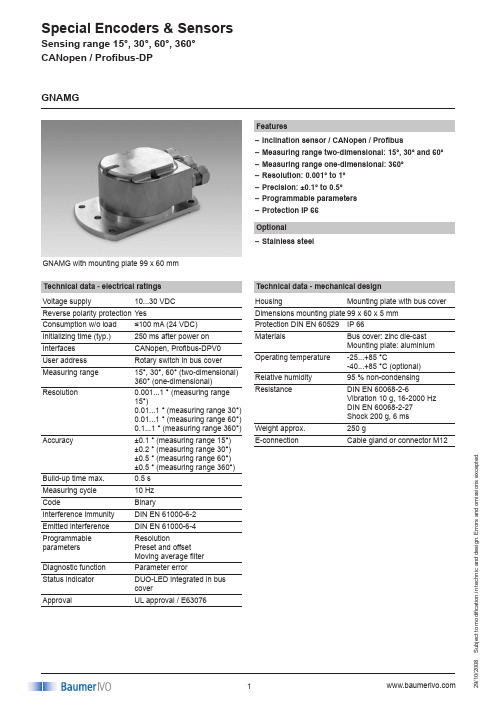
S u b j e c t t o m o d i fi c a t i o n i n t e c h n i c a n d d e s i g n . E r r o r s a n d o m i s s i o n s e x c e p t e d .008GNAMG with mounting plate 99 x 60 mm FeaturesInclination sensor / CANopen / Profibus–Measuring range two-dimensional: 15°, 30° and 60° –Measuring range one-dimensional: 360° –Resolution: 0.001° to 1° –Precision: ±0.1° to 0.5° –Programmable parameters –Protection IP 66 –Technical data - electrical ratings Voltage supply 10...30 VDC Reverse polarity protection YesConsumption w/o load ≤100 mA (24 VDC)Initializing time (typ.)250 ms after power on Interfaces CANopen, Profibus-DPV0User address Rotary switch in bus cover Measuring range 15°, 30°, 60° (two-dimensional) 360° (one-dimensional)Resolution0.001...1 ° (measuring range 15°)0.01...1 ° (measuring range 30°) 0.01...1 ° (measuring range 60°) 0.1...1 ° (measuring range 360°)Accuracy±0.1 ° (measuring range 15°) ±0.2 ° (measuring range 30°) ±0.5 ° (measuring range 60°) ±0.5 ° (measuring range 360°)Build-up time max.0.5 s Measuring cycle 10 Hz CodeBinaryInterference immunity DIN EN 61000-6-2Emitted interference DIN EN 61000-6-4Programmable parameters ResolutionPreset and offset Moving average filter Diagnostic function Parameter errorStatus indicator DUO-LED integrated in bus coverApprovalUL approval / E63076GNAMGTechnical data - mechanical design HousingMounting plate with bus cover Dimensions mounting plate 99 x 60 x 5 mmProtection DIN EN 60529IP 66MaterialsBus cover: zinc die-cast Mounting plate: aluminium Operating temperature -25...+85 °C-40...+85 °C (optional)Relative humidity 95 % non-condensing ResistanceDIN EN 60068-2-6Vibration 10 g, 16-2000 Hz DIN EN 60068-2-27 Shock 200 g, 6 ms Weight approx.250 gE-connectionCable gland or connector M12Optional Stainless steel–S u b j e c t t o m o d i fi c a t i o n i n t e c h n i c a n d d e s i g n . E r r o r s a n d o m i s s i o n s e x c e p t e d .008GNAMGPart number GNAMG.Interface5P32CANopen / cable gland 5PA2CANopen / connector M12 3P32Profibus-DPV0 / cable gland3PA2Profibus-DPV0 / connector M12Measuring range 21Dual axes ±15° 22Dual axes ±30° 23Dual axes ±60°15Single axis 360° (no end stop)Housing0Bus cover with mounting plate99 x 60 mmAccessoriesConnectors and cables (page %S)Z 180.005Female connector M12, 5-pin, 5 m cable Z 180.007Female connector M12, 5-pin, 10 m cable Z 181.005Cable connector M12, 5-pin, 5 m cable Connection M2 / M3, continuative bus Programming accessories (page %S)Z 150.022CD with describing files & manualsCANopen – M12 connector Connector Assignment Description Pin 1 GND Ground connection relating to UB Pin 2 UB Voltage supply 10...30 VDC Pin 3 – –Pin 4 CAN_H CAN bus signal (dominant High)Pin 5CAN_LCAN bus signal (dominant Low)12345M12 connector (male / female)A-codedProfibus – M12 connectorPin 1 UB Voltage supply 10...30 VDC Pin 3 GNDGround connection relating to UBPin 2A Negative data linePin 4 BPositive data line43512Terminals of the same significance are internally connected and identical in their functions. Max. load on the internal terminal connections UB-UB and GND-GND is 1 A each.M12 connector (male)A-codedM12 connector (male / female)B-codedTerminal assignment CD with file descriptions is not included in the delivery. You may order them on CD as accessory free-of-charge.Su b j ectt o m o d i fi c a t i o n i n t e c h n i c a n d d e s i g n . E r r o r s a n d o m i s s i o n s e x c e p t e d .008Y XZ +Default 0º Measured inclination -30º Default 0º Measured inclination 30ºThe two-dimensional inclination sensor with a confi gured range of 15°, 30° and 60° must be mounted with the base plate in horizontal position, i.e. parallel to the horizontal line. The inclination sensor may also be installed upside down, i.e. turned by 180°.The sensor can be inclined both towards the X and Y axis at the same time.For each axis a separate measured value is provided. Default on delivery the inclination sensor will apply the selected sensing range to both axis, for example ±15° with the zero passage being precisely in the horizontal line.The inclination sensor with a confi gured range of 360º must be mounted in a way that the X-axis as in the following sketch is directed in a parallel way towards gravity. The defl ection may not be more than ±3º.Please note also that the inclination sensor must evenly touch the contact surface and during inclination/rotation must not be subject to any inclination in X- or Y-direction since this would have a negative impact on the measu-ring accuracy.The 360° inclination sensor default position is 0° as shown in the following illustration but may be confi gured at will by help of the preset function. The measuring direction may also be inverted. Default on delivery theinclination sensor’s sensing direction is clockwise from 0...360°, in case of active inversion counter-clockwise.Measuring range 15º, 30º, 60ºMeasuring range 360ºDefault 0ºMeasured inclination 45ºMeasured inclination 135ºMeasured inclination 180ºInstallation positionGNAMGS u b j e c t t o m o d i fi c a t i o n i n t e c h n i c a n d d e s i g n . E r r o r s a n d o m i s s i o n s e x c e p t e d .008Dimensions CANopen connector M12Profibus connector M12GNAMG cable glandGNAMG。

210.00 mmE E 0 0' 0£�AC-25 Portable Battery-Operated Acoustic AmpUser ManualFCC WARNINGThis device complies with part 15 of the FCC Rules. Operation is subject to the following two conditions: (1) this device may not cause harmful interference, and (2) this device must accept any interference received, including interference that may cause undesired operation.Any changes or modifications not expressly approved by the party『esponsible for compliancecould void the use「's authority to operate the equipment.NOTE: This equipment has been tested and found to comply with the limits for a Class B digital device, pursuant to Part 15 of the FCC Rules. These limits are designed to provide reasonable protection against harmful interference in a residential installation. This equipment generates, uses and can radiate radio frequency ene「gy and, if not installed and used in accordance with the instructions, may cause harmful interference to radio communications. However, there is no guarantee that interference will not occur in a particular installation.If this equipment does cause harmful interference to radio or television reception,which can be determined by turning the equipment off and on, the user is encouraged to try to correct the interference by one or more of the following measures:-Reorient or relocate the receiving antenna.-Increase the separation between the equipment and receiver.-Connect the equipment into an outlet on a circuit different from that to which the receiver is connected.-Consult the dealer or an experienced radio/TV technician for help.FCC RF exposure statement:The device has been evaluated to meet general RF exposure requirement. The device can be used in portable exposure condition without restriction.Int『oduction The NUX AC-25 is a portable battery-operated amplifier optimized for acoustic-electric guitars. It features 2 channels withseparate controls, Bluetooth connectivity, onboard tuner and a dedicated tone editing app. Where there is AC-25 there is music.Features• 2 channels with separate controls•Onboard Reverb Effects & Tuner• Up to 4 hours of continuous playing time•Bluetooth Connectivity for audio streaming and tone editing• Well-planed controls & 1/0Cont『ol Panels CHANNEL 101 CHANNEL2 COMBO JackCHANNEL 2 VOLUME Knob BASS Knob MIDDLE Knob TREBLE Knob TUNER Button Dis p layQ)Q) Q) Q) 0V口LUME BASS MIDDLE TREBLE TUNERVOLUME Knob SEND Knob REVERB Knob MASTER Knob BLUETOOTH ON/OFFF SwitchButtonChannel1INPUT Jack¼"(6.35mm) INPUT Jack, accept both passive andactive acoustic pickups.VOLUME KnobControls the input signal level for the Channel 1 input.BASS KnobBass frequency level control.MIDDLE KnobMiddle frequency level control.TREBLE KnobTreble frequency level control.TUNER ButtonPress this button to engage/disengage the built-intuner.Control PanelsDisplayTuning display. For further information please refer tothe TUNER description.Channel2COMOBO JackXLR input or 1/4"(6.35mm) instrument input.VOLUME KnobControls the input signal level for the Channel 2 input.SEND KnobAdjusts the amount of reverb.Global ControlsREVERB KnobSets the overall reverb .MASTER KnobSets the overall output volume level.02Control Panels Rear Panel BLUETOOTH ButtonPress this button to engage/disengage the built-inBluetooth function.For further information please refer to the Bluetoothdescription.POWER indicatorLights on steady when the amplifier is on.ON/OFFF SwitchTurn ON/OFF the amplifier.DC-IN Jack *Please turn down the mater volume before you turn on the amp.NU�XAC-2巴FCCNm兰呈iDF~NDB-主i uND呈一THi口之5主MAY呈HATTTON巨三一兰ANYONC-iiRFi等圭ACC-i_髻MADE IN CHINA CE: 互@INx1uA LIN匾口UTCharge Indicator Low Batt. PHONES JackIndicatorAUX-IN Jack LINE OUT Jack03 04Rear PanelDC-IN JackPlug in the included power supply here to power/charge this amplifier.Use specified power supply only(DC 15V/2.5A Polarity: Negative tip).Charge lndicato『Lights on steady du『ing the charging process.Lights off automatically when the battery is fully charged. Low Batt. lndicato『The LED indicator will light on when the battery level is low. For further information, please refer to the BATTERY description.PHONES Jack¼Composite audio signal output jack.NOTE: The amplifier will be muted when it's plugged in.05 AUX-IN Jack1/8 Line level AUX-IN jack.You can connect a CD player, MP3 player, or other deviceand play back sounds in stereo.LINE OUT JackYou can connect a mixer, recording device, or other suchdevice here.SPEAKERCoverSPEAKERSTANDMain PartsSPEAKER CoverYou can take off the speaker cover by pulling the ribbonon lower right corner.SPEAKER6.5" inch full range speaker. + sound hole.STANDYou can use the folding stand, just pull it up whenneeded.06Operation GuideTUNERConnections & Examples of using AC-25二TUNING MODE F凶T SHARP IN TUNE 1.Press the TUNER button to active the built-in tuner.2.Adjust tuning peg of each string according to the tuning visuals on the DISPLAY:3.When finishing up, press the TUNER button again to quite the tuner mode.*The amplifier will be muted when TUNER is engaged.*Tuner ONLY works with CHANNEL 1.BLUETOOTH ®1.When you power on the amplifier the Bluetooth function will also be turned on automatically by default. You can turn off the Bluetooth function manually by holding down the BULETOOTH button for 2 seconds.072.This green indicator will keep flash indicating the Bluetooth®module is ready for pairing.3.Go to the Bluetooth setting menu of Bluetooth enabled device, find the device named "NUX AC25", tap to pair.You will hear an cue tone when connection established successfully.BATTERYThis amplifier is equipped with rechargeable battery packs. You can use either the built in battery packs or the included power supply to power up the amplifier. The Low Batt. indicator will light on when the battery level is low. At this point, the amplifier cannot be powered up until the power supply has been plugged in to recharge the battery. The amplifier can be used normally while charging. After the battery is fully charged, this indicator will turn off automatically.A full charge can take up to 4 hours, a full charge allows up to 4 hours of use.*Use time may vary depending on your settings.GuitarChannel 1口_。
Eaton KDB3225WEaton Series C complete molded case circuit breaker, K-frame, KDB, Complete breaker, Fixed thermal, fixed magnetic trip type, Three-pole, 225A, 600 Vac, 250 Vdc, 65 kAIC at 240 Vac, 35 kAIC at 480 Vac, Without terminals, 50/60 HzGeneral specificationsEaton Series C complete molded case circuit breakerKDB3225W 7866796121014.1 in5.5 in5.5 in 11.5 lb Eaton Selling Policy 25-000, one (1) year from the date of installation of the Product or eighteen (18) months from the date of shipment of the Product, whichever occurs first.UL Listed Product NameCatalog Number UPCProduct Length/Depth Product Height Product Width Product Weight WarrantyCertificationsSeries C35 kAIC at 480 Vac65 kAIC at 240 VacKKDB50 to 60 HzComplete breakerWithout terminals600 Vac, 250 Vdc225 AFixed thermal, fixed magnetic Three-pole Application of Tap Rules to Molded Case Breaker Terminals Application of Multi-Wire Terminals for Molded Case Circuit Breakers UL listed 100%-rated molded case circuit breakersMOEM MCCB Product Selection GuideStrandAble terminals product aidCurrent limiting Series C molded case circuit breakers product aid Circuit breaker motor operators product aidPlug-in adapters for molded case circuit breakers product aidMulti-wire lugs product aidMotor protection circuit breakers product aidPower metering and monitoring with Modbus RTU product aid Breaker service centersMolded case circuit breakers catalogEaton's Volume 4—Circuit ProtectionInstruction Leaflet for the KES 310+ Electronic Trip Unit Installation Instructions for DK, KDB, KD, HKD, KDC, KW, HKW, KWC, CKD, CHKD Circuit Breakers and Molded Case SwitchesCircuit breakers explainedCircuit Breakers ExplainedSeries C J-Frame molded case circuit breakers time current curves Series C G-Frame molded case circuit breakers time current curves MOEM MCCB product selection guideEaton Specification Sheet - KDB3225WF-Frame 310+ Molded-case circuit breakers 15-225ASeries C F-Frame molded case circuit breakersSeriesInterrupt ratingFrameCircuit breaker type Frequency ratingCircuit breaker frame type TerminalsVoltage rating Amperage RatingTrip TypeNumber of poles Application notesBrochuresCatalogsInstallation instructions MultimediaSpecifications and datasheetsEaton Corporation plc Eaton House30 Pembroke Road Dublin 4, Ireland © 2023 Eaton. All Rights Reserved. Eaton is a registered trademark.All other trademarks areproperty of their respectiveowners./socialmedia。