MAX472CSA-T中文资料
- 格式:pdf
- 大小:137.71 KB
- 文档页数:13
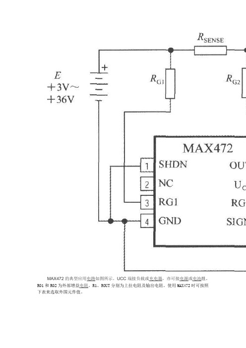
MAX472的典型应用电路如图所示。
UCC端接负载或充电器,亦可接电源或电池组。
RG1和RG2为外部增益电阻。
R1、ROUT分别为上拉电阻及输出电阻。
使用MAX472时可按照下表来选取外围元件值。
【收藏此页】【关闭】【返回】【打印】MP25P1171344:一、前言伴随着城市人口和建设规模的扩大,各种用电设备的增多,用电量越来越大,城市的供电设备经常超负荷运转,用电环境变得越来越恶劣,对电源的“考验”越来越严重。
据统计,每天,用电设备都要遭受 120 次左右各种的电源问题的侵扰,电子设备故障的 60% 来自电源 [7] 。
因此,电源问题的重要性日益凸显出来。
原先作为配角,资金投入较少的电源越来越受到厂商和研究人员的重视,电源技术遂发展成为一门崭新的技术。
而今,小小的电源设备已经融合了越来越多的新技术。
例如开关电源、硬开关、软开关、参数稳压、线性反馈稳压、磁放大器技术、数控调压、 PWM 、 SPWM 、电磁兼容等等。
实际需求直接推动电源技术不断发展和进步,为了自动检测和显示电流,并在过流、过压等危害情况发生时具有自动保护功能和更高级的智能控制,具有传感检测、传感采样、传感保护的电源技术渐成趋势,检测电流或电压的传感器便应运而生并在我国开始受到广大电源设计者的青睐,本文主要介绍 ABB 公司的电流传感器。
二、电流传感器的工作原理 [1]ABB 公司的电流传感器可以测量各种类型的电流,从直流电到几十千赫兹的交流电,其所依据的工作原理主要是霍尔效应,如图 1 所示。
当原边导线经过电流传感器时,原边电流 I P 会产生磁力线①,原边磁力线集中在磁芯②周围,内置在磁芯气隙中的霍尔电极③可产生和原边磁力线①成正比的大小仅几毫伏的电压,电子电路④可把这个微小的信号转变成副边电流 I S ⑤,并存在以下关系式其中, I S —副边电流;I P —原边电流;N P —原边线圈匝数;N S —副边线圈匝数;N P / N S —匝数比,一般取 N P =1 。

M A X471M A X472的中文资料大全(总4页)-本页仅作为预览文档封面,使用时请删除本页-MAX471/MAX472的特点、功能美国美信公司生产的精密高端电流检测放大器是一个系列化产品,有MAX471/MA X472、 MAX4172/MAX4173等。
它们均有一个电流输出端,可以用一个电阻来简单地实现以地为参考点的电流/电压的转换,并可工作在较宽电压内。
MAX471/MAX472具有如下特点:●具有完美的高端电流检测功能;●内含精密的内部检测电阻(MAX471);●在工作温度范围内,其精度为2%;●具有双向检测指示,可监控充电和放电状态;●内部检测电阻和检测能力为3A,并联使用时还可扩大检测电流范围;●使用外部检测电阻可任意扩展检测电流范围(MAX472);●最大电源电流为100μA;●关闭方式时的电流仅为5μA;●电压范围为3~36V;●采用8脚DIP/SO/STO三种封装形式。
MAX471/MAX472的引脚排列如图1所示,图2所示为其内部功能框图。
表1为MAX471/MAX472的引脚功能说明。
MAX471的电流增益比已预设为500μA/A,由于2kΩ的输出电阻(ROUT)可产生1V/A的转换,因此±3A时的满度值为3V.用不同的ROUT电阻可设置不同的满度电压。
但对于MAX471,其输出电压不应大于VRS+。
对于MAX472,则不能大于。
MAX471引脚图如图1所示,MAX472引脚图如图2所示。
MAX471/MAX472的引脚功能说明引脚名称功能MAX471MAX47211SHDN关闭端。
正常运用时连接到地。
当此端接高电平时,电源电流小于5μA2,3-RS+内部电流检测电阻电池(或电源端)。
“+”仅指示与SIGN输出有关的流动方向。
封装时已将2和3连在了一起-2空脚-3RG1增益电阻端。
通过增益设置电阻连接到电流检测电阻的电池端44GND地或电池负端55SIGN集电极开路逻辑输出端。

FEATURES AND SPECIFICATIONS SPECIIFICATIONS Battery Connector47182Vertical, SMT 47204Right Angle, SMT 47274Right Angle, SMT 47280Right Angle, SMT 48232Parallel, SMTMolex offers Battery Connectors for mobile applications.In mobile applications, battery efficiency plays an important part in the utilization time of the device. Proper battery contact, efficient electrical properties, physical size of connector are some of the major design considerations.Working together with major customers in the mobile device markets, Molex has developed a comprehensive range of battery connectors that addresses most of these applications design concerns. With working heights of 1.50mm to 5.50mm and circuit sizes of 2 to 5, Molex’s battery connectors brings forth flexibility in design solutions for the customers.4718247204472744823247280Reference InformationPackaging: Refer to order tableUL File No.:CSA File No.:Mates With:Designed In:mmElectricalVoltage: Refer to order tableCurrent: Refer to order tableContact Resistance: Refer to order tableDielectric Withstanding Voltage: Refer to ordertableInsulation Resistance: Refer to order tableMechanicalContact Insertion Force:47182, 47274, 47204 : 1.02N (0.67lb)Durability: Refer to order tablePhysicalHousing: Thoermoplastic, JL 94V-0Contact:47182, 47204, 47274, 48232 Copper (Cu)Alloy47280 Beryllium Copper (BeCu)Plating:Contact Area —Refer to order tableUnderplating—Nickel (Ni)Operating Temperature: Refer to order tableORDERING INFORMATIONBringing People & Technology Together, Worldwide SMVisit our Web site at Americas Headquarters 2222 Wellington Ct.Lisle, Illinois 60532 USA 1-800-78MOLEX amerinfo@Far East North Headquarters Yamato, Kanagawa, Japan 81-462-65-2324feninfo@Far East South Headquarters Jurong, Singapore 65-6-268-6868fesinfo@European Headquarters Munich, Germany 49-89-413092-0eurinfo@Corporate Headquarters 2222 Wellington Ct.Lisle, Illinois 60532 USA 630-969-4550MARKETS AND APPLICATIONS Order No. SNG-059©2006, MolexBattery Connector 47182Vertical, SMT 47204Right Angle, SMT 47274Right Angle, SMT 47280Right Angle, SMT 48232Parallel, SMT•Mobile phones •PDAs•Handheld GPS unitsMobile PhonesPDAsHandheld GPS。


Approval Standard And Recognized NO.CB Part Number Configuration :JY 102 K Y5P Y2(1) AC capacitors, safety(4) Type code: Y5P, Y5V,Y5U(1) (2) (3) (4) (5)(2) Rated capacitance (5) Class Y2(3) Tolerance on rated capacitance3JYH HSU Y2 SERIESINTRODUCTIONThese Ceramic Disc Capacitors are specifically designed for AC applications and meet the safety requirements of various safety standards agencies.These capacitors are ideal for acrossFEATURES:⊙Ideal for across the line applictions ⊙Compact size⊙Cost effective product⊙Safety standards recognized for AC applicationsCAPACITANCE AND DIMENSIONS:When ordering safety standard recognized ceramic capacitors please use the part number as noted aboveMARKINGJEC TYPE DESIGNATION or JD ( for Y1) 3 - DIGIT - SYSTEM : 472 = 4700 PF : 103 = 10000 PF CODE : K =Dimensions and Tolerance B = 3.0 mm max for AA d =0.55 mm ±0.05 mm F = 7.5 or 9.5 ±0.8 mm L =3 ~ 33 mm.◎ According as customer's request and size.Y2 , X1 ,AC300V , AC400V5新版1:新版2:加 KCWhether to put a KC logo according to customer's request按客户要求是否要加印 KC 标志MARKING : (FOR Y2)旧版6文件編號:P004 版 本:5 制訂日期:2014/02/20JECJY 102 KJEC JY 102 KJY 103 MJEC成品之編碼原則上以十五碼完成,亦以阿拉伯數字與英文字母混合編成,文件編號:P004碼至第十一碼與瓷片相同。

MAX16147WM75SA+MAX16147WM75SA+TGeneral DescriptionThe MAX16143, MAX16145, MAX16147, and MAX16149 are supervisory circuits that monitor their own supply voltages using a factory-set reset threshold that ranges from +2.3V to +11.6V. A manual reset (MR or MR ) input is included. The RESET (or RESET ) output has options for active-low, active-high, push-pull, or open-drain. The reset output asserts when the monitored voltage falls below the threshold voltage, and remains asserted until the monitored voltage has exceeded its threshold (plus hysteresis) for a time equal to the factory-set reset time-out period. Available reset timeout periods range from 30µs to 4.2s.The 5-pin SOT23 and 4-bump wafer-level packages (WLPs) offer compatibility with space-constrained environments. These ICs are fully specified over the -40°C to +125°C temperature range.Applications●Servers●Communications Equipment ●Industrial EquipmentOrdering Information appears at end of data sheet.19-100361; Rev 1; 6/18Benefits and Features●Factory-Set Reset Threshold Options from +2.3V to+11.6V ●Manual Reset Input• Active-High and Active-Low Trigger Options • Optional Internal Pullup or Pulldown• Fast (45µs) and Slow (50ms) Debounce Time Options ●Guaranteed Reset Valid to V CC ≥ 1.3V●Push-Pull and Open-Drain Reset Output Options• M AX16143: Open-Drain, Active-Low • MAX16145: Open-Drain, Active-High • MAX16147: Push-Pull, Active-Low • MAX16149: Push-Pull, Active-High ●Power-Supply Transient Immunity●-40°C to +125°C Operating Temperature Range ●SOT23-5 Package and 4-Bump WLPsSimplified Block DiagramClick here for production status of specific part numbers.MAX16143/MAX16145/MAX16147/MAX16149High-Voltage Supervisors with Manual Reset InputEVALUATION KIT AVAILABLEV CC to GND ..........................................................-0.3V to +15V MR or MR to GND .............-0.3V to lower of VCC + 0.3 or 6.0 V RESET or RESET to GND ....-0.3V to lower of V CC +0.3 or 6.0V Input/Output Current (All pins) ........................-20mA to +20mA Continuous Power Dissipation (Multilayer Board, SOT23, T A = +70°C, derate 3.9mW/°Cabove +70°C.) .............................................................312.6mWContinuous Power Dissipation (Multilayer Board,WLP , T A = +70°C, derate 9.7mW/°C above +70°C.) ....776mW Operating Temperature Range .........................-40°C to +125°C Storage Temperature Range ............................-65°C to +150°CSOT-23PACKAGE CODEU5+1Outline Number 21-0057Land Pattern Number90-0174Thermal Resistance, Single-Layer Board:Junction to Ambient (θJA )324.3Junction to Case (θJC )82Thermal Resistance, Four-Layer Board:Junction to Ambient (θJA )255.9Junction to Case (θJC )81WLPPACKAGE CODEW40E0+1Outline Number 21-100215Land Pattern NumberSee App Note 1891Thermal Resistance, Four-Layer Board:Junction to Ambient (θJA )103°C/W Junction to Case (θJC )N/A Absolute Maximum RatingsStresses beyond those listed under “Absolute Maximum Ratings” may cause permanent damage to the device. These are stress ratings only, and functional operation of the device at these or any other conditions beyond those indicated in the operational sections of the specifications is not implied. Exposure to absolute maximum rating conditions for extended periods may affect device reliability.Package thermal resistances were obtained using the method described in JEDEC specification JESD51-7, using a four-layer board. For detailed information on package thermal considerations, refer to /thermal-tutorial .For the latest package outline information and land patterns (footprints), go to /packages . Note that a “+”, “#”, or “-” in the package code indicates RoHS status only. Package drawings may show a different suffix character, but the drawing pertains to the package regardless of RoHS status.Package InformationMAX16143/MAX16145/ MAX16147/MAX16149High-Voltage Supervisors with Manual Reset Input(V CC = 2.3V to 14V, T J = T A = -40°C to +125°C, Typical values are at T A = 25°C unless otherwise noted. Limits over the operating temperature range and relevant supply voltage range are guaranteed by design, test, and characterization.)Note 2: Correct reset output voltage is guaranteed down to V CC = 1.3V.Note 3: During power-up, the internal regulator takes 2ms. Power-up time must be added to reset timeout period.PARAMETERSYMBOL CONDITIONSMIN TYPMAX UNITSOperating Voltage RangeV CCCorrect threshold detection3.314V MAX16143, MAX16147 (active-low). Correct reset state for supply ramp time ≥ 20µs. (Note 2) 1.314MAX16145, MAX16149 (active-high). Correct reset state for supply ramp time ≥ 1ms.214Supply CurrentI CC V CC ≤ V TH + 150mV2555µA Reset Threshold AccuracyV TH_ACC-1.5+1.5%Reset Threshold HysteresisHysteresis option Q, V CC rising0.5%V THHysteresis option R, V CC rising 1Hysteresis option S, V CC rising 3Hysteresis option T, V CC rising5V CC to Reset Output Delay t RDV CC falling at 10mV/µs from (V CC + 100mV) to (V CC - 100mV)15µs Reset Timeout Period Accuracy (Note 3)Variation from nominal t RP -25+25%Output Voltage Low V OL V CC ≥ 1.7V, I SINK = 3.2mA 0.4V 1.3V ≤ V CC < 1.7V, I SINK = 100µA 0.4Output Voltage High V OH MAX16147/MAX16149, I SOURCE = 10μA 2.4 3.15V Output CurrentI OH V OH = 2.5V255080µA Open-Drain Output Leakage CurrentMAX16143/MAX161451µA Manual Reset Debounce Timet DB Active-low or active-high manual reset 4570µs 5070ms Manual Reset Minimum Input Pulse Width t PW Edge-triggered manual reset option.—µs MR Internal Pullup Resis-tanceR PU MR option F or H 50kΩMR Internal Pulldown Re-sistanceR PD MR option B or D 50kΩInput Voltage Low V IL MR, MR 0.7V Input Voltage High V IH MR, MR1.7V Input CurrentMR, MR . Internal pullup resistor not connected.-150+150nA Electrical CharacteristicsMAX16143/MAX16145/ MAX16147/MAX16149High-Voltage Supervisors with Manual Reset Input(T A = 25°C unless otherwise noted.)Typical Operating CharacteristicsMAX16143/MAX16145/ MAX16147/MAX16149High-Voltage Supervisors with Manual Reset Input(T A = 25°C unless otherwise noted.)Typical Operating Characteristics (continued)1101001000MAXIMUM V CC TRANSIENT DURATION vs. OVERDRIVEtoc112V/div20ms/divRST 2V/div 2V/divV CC = 12Vtoc09MAX16143/MAX16145/ MAX16147/MAX16149High-Voltage Supervisors with Manual Reset Input(T A = 25°C unless otherwise noted.)Typical Operating Characteristics (continued)toc162ms/divV CC RISE TIME = 10ms1V/divRESETtoc14500µs/div1V/divV BACKUPV CC RISE TIME = 100µs1V/divRESETtoc1720ms/div1V/divCCV CC RISE TIME = 100ms1V/divtoc151V/divV CC RISE TIME = 1msMAX16143/MAX16145/ MAX16147/MAX16149High-Voltage Supervisors with Manual Reset InputPINNAME FUNCTIONSOT23WLP 1A1RESET, RESET Reset Output. RESET asserts when V CC falls below the factory-set threshold or when the manual reset is triggered. RESET deasserts after the factory-set reset timeout when V CC goes above its set threshold or when MR is released.2, 4B2GND Ground3B1MR, MR Manual Reset Input. See Manual Reset Input section for more detail.5A2V CCSupply Voltage Input. Bypass V CC to ground with a 0.1µF capacitor.Pin ConfigurationPin DescriptionMAX16143/MAX16145/ MAX16147/MAX16149High-Voltage Supervisors with Manual Reset InputDetailed DescriptionThe MAX16143/MAX16145/MAX16147/MAX16149 aresupervisory circuits that monitor their V CC voltage from+2.3V to +11.6V using factory-set reset threshold andoffer manual reset capability. The MAX16143/MAX16145feature an open-drain reset output, while the MAX16147/MAX16149 feature a push-pull reset output. The resetoutput asserts and remains asserted for the reset timeoutafter the V CC voltage exceeds its threshold. All devicesare offered with reset timeout periods ranging from 30μsto 4200ms. See Table 1 for available options. The resetoutput is guaranteed to be in valid logic state down toV CC = 1.3V.V CC ThresholdThe MAX16143/MAX16145/MAX16147/MAX16149operate with a V CC supply voltage from +3.3V to +14V,with monitoring range of +2.3V to +11.6V. V CC has arising threshold of V TH + V HYST and a falling thresholdof V TH. See Tables 2 and 3 for available threshold andhysteresis options. When V CC rises above V TH + V HYSTand the manual reset input is in an inactive state, RESETdeasserts after the reset timeout period (t RP). See thetiming diagram in Figure 1. When V CC falls below V TH,the reset output asserts low after a fixed delay (t RD).Table 1. Reset Timeout OptionsTable 2. V CC Threshold OptionsSUFFIXRESET TIMEOUTPERIODUNIT T A = 25°CT A = -40°Cto +125°CTYP MIN MAXA30——µs B 1.50 1.125 1.875ms C3 2.25 3.75ms D6 4.57.5ms E12915ms F241830ms G5037.562.5ms H10075125ms I150112.5187.5ms J225168.8281.3ms K300225375ms L450337.5562.5ms M600450750ms N10007401250ms O200015002500ms P420031505250ms SUFFIX1.5%UNITTYP MIN MAXY611.48411.60011.716V Y511.38511.50011.615V Y411.28611.40011.514V Y311.18711.30011.413V Y211.08811.20011.312V Y110.98911.10011.211V Y010.8911.00011.11V X710.59310.70010.807V X610.49410.600107.06V X510.39510.50010.605V 009.910.00010.1V 959.4059.5009.595V 908.919.0009.09V 858.4158.5008.585V 807.928.0008.08V 757.4257.5007.575V70 6.937.0007.07V65 6.435 6.500 6.565V60 5.94 6.000 6.06V55 5.445 5.500 5.555V48 4.752 4.800 4.848V47 4.653 4.700 4.747V46 4.554 4.600 4.646V45 4.455 4.500 4.545V44 4.356 4.400 4.444V43 4.257 4.300 4.343V42 4.158 4.200 4.242V41 4.059 4.100 4.141V40 3.960 4.000 4.040V39 3.861 3.900 3.939V38 3.762 3.800 3.838V37 3.663 3.700 3.737V36 3.564 3.600 3.636V35 3.465 3.500 3.535V34 3.366 3.400 3.434V33 3.267 3.300 3.333V32 3.168 3.200 3.232V31 3.069 3.100 3.131V30 2.970 3.000 3.030V29 2.871 2.900 2.929VMAX16143/MAX16145/ MAX16147/MAX16149High-Voltage Supervisors with Manual Reset InputReset OutputThe MAX16143/MAX16145 feature open-drain reset outputs, while the MAX16147/MAX16149 feature push-pull reset outputs. For proper operation, connect the reset output of the MAX16143 and the MAX16145 to V CC , or external voltage with a pullup resistor. The reset output of the MAX16147 and the MAX16149 are internally connected to a 2.5V or 3V regulator.Manual Reset InputThe MAX16143/MAX16145/MAX16147/MAX16149 include a manual reset input (MR, MR ) that allows initiating system reset using external signal or push-button switch. The manual reset input is available in active-low, active-high or edge-triggered option. The active-low (MR ) and active-high (MR) inputs feature either 45μs or 50ms debounce timing option to help filter out noise during manual reset transitioning from inactive to active state. In addition, the manual reset input is factory-programmable to have a pull up/pull down resistor or be left floating. See Table 4 and Table 5 for available options.Table 2. V CC Threshold Options (continued)Table 3. V CC Threshold Hysteresis OptionsTable 4. MAX16143/MAX16145 Manual Reset Configuration OptionsSUFFIX 1.5%UNIT TYP MIN MAX 28* 2.772 2.800 2.828V 27 2.673 2.700 2.727V 26* 2.574 2.600 2.626V 25 2.475 2.500 2.525V 24 2.376 2.400 2.424V 232.2772.3002.323VSUFFIX HYSTERSISQ 0.5%R 1%S 3%T5%SUFFIXLEVEL HIGH/LOWDEBOUNCE TIME (NA = EDGE TRIGGER)PULLUP/PULLDOWN A H 45µs NOT CONNECTEDB H 45µs PULLDOWNC H 50ms NOT CONNECTEDD H 50ms PULLDOWNE L 45µs NOT CONNECTEDF L 45µs PULLUPG L 50ms NOT CONNECTEDH L 50ms PULLUP J H N/A NOT CONNECT K H N/A PULLDOWN L L N/A NOT CONNECTEDMLN/APULL UPMAX16143/MAX16145/ MAX16147/MAX16149High-Voltage Supervisors with Manual Reset InputTable 5. MAX16147/MAX16149 Manual Reset and RESET Configuration OptionsSUFFIX LEVELHIGH/LOW DEBOUNCE TIME(NA = EDGETRIGGER)MR/MRPULLUP/PULLDOWNRESETPULLUPVOLTAGEA H45µs NOT CONNECTED3VB H45µs PULLDOWN3VC H50ms NOT CONNECTED3VD H50ms PULLDOWN3VE L45µs NOT CONNECTED3VF L45µs PULLUP3VG L50ms NOT CONNECTED3VH L50ms PULLUP3VJ H N/A NOT CONNECTED 2.5VK H N/A PULLDOWN 2.5VL H N/A NOT CONNECTED 2.5VM H N/A PULLUP 2.5VN L45µs NOT CONNECTED 2.5VO L45µs PULLUP 2.5VP L50ms NOT CONNECTED 2.5VQ L50ms PULLUP 2.5VR H N/A NOT CONNECTED3VS H N/A PULLDOWN3VT L N/A NOT CONNECTED3VU L N/A PULLUP3VV H N/A NOT CONNECTED 2.5VW H N/A PULLDOWN 2.5VX L N/A NOT CONNECTED 2.5VY L N/A PULLUP 2.5V MAX16147/MAX16149with Manual Reset InputApplications InformationReset OutputThe MAX16143/MAX16145/MAX16147/MAX16149 are microprocessor supervisory circuits that assert a reset to prevent code-execution errors during power-up, power-down, and brownout conditions. The reset output asserts when the V CC voltage falls below the factory-set threshold, V TH . The reset output de-asserts after the reset timeout (t RP ) when V CC voltage rises above the reset threshold plus the hysteresis voltage, (V TH + V HYST ). The reset output is guaranteed to be at the correct logic voltage for VCC voltage down to 1.3V. See Figure 1 for details.Manual Reset Input (MR)Many systems require manual reset capability, allowing the operator, a test technician, or external logic circuitry to initiate a reset. The MAX16143/MAX16145/MAX16147/MAX16149 provide this capability by featuring an manual reset input (MR). When a manual reset is initiated, the reset output asserts and remain asserted as long as the manual reset input is in active state. Reset deasserts after reset timeout when the manual reset input is released. Figure 1 shows the behavior of the manual reset configured as active-low, with 50kΩ pull (MR ). See Selector Guide for available options.Depending on the application, the manual reset input is factory-programmable to have either an internal pullup resistor, pulldown resistor of 50kΩ (typ), or be left floating.The pullup resistor allows the manual reset input to be left unconnected if not used. An external pullup resistor is required if the manual reset input option chosen does not have an internal pullup resistor. The maximum input voltage on MR is 5.5V.An alternative is to use a normally open momentary switch connected from MR (active-low) to GND, or from MR (active-high) to a logic-high voltage to create a manual-reset function. If a Long Debounce version is used, external debounce circuitry is not required, but an external pullup or pulldown will be required if a version without an internal resistor is used. If the manual reset input is driven from long cables, or the IC is used in a noisy environment, connect a 0.1μF capacitor from MR /MR to GND in order to provide additional noise immunity.Negative-Going V CC Transients ProtectionThese supervisory circuits are relatively immune to short-duration, negative-going V CC transients (glitches). The Maximum Transient Duration vs. Reset Threshold Overdrive graph (in the Typical Operating Characteristics section) shows the typical transient pulse width and amplitude required to trigger a reset. The reset threshold overdrive specifies how far the pulse falls below the actual reset threshold, and the maximum transient duration specifies the width of the pulse as it crosses the reset threshold. If a pulse occurs in the region above the curve, a reset triggers. If a pulse occurs in the region below the curve, a reset does not trigger.Figure 1. RESET and MR Timing DiagramMAX16147/MAX16149with Manual Reset InputMAX16147/MAX16149with Manual Reset Input*Future product—Contact factory for availability.+ Denotes a lead(Pb)-free/RoHS-compliant package. T Denotes tape-and-reel.PARTTEMP RANGE PIN-PACKAGEMAX16143_ _ _ _ _+T*-40°C to +125°C 4 WLP MAX16145_ _ _ _ _ T*-40°C to +125°C 4 WLP MAX16147WM75SA+T -40°C to +125°C 4 WLP MAX16149_ _ _ _ _T*-40°C to +125°C4 WLPTypical Application CircuitOrdering InformationMAX16147/MAX16149with Manual Reset InputREVISION NUMBERREVISION DATEDESCRIPTIONPAGES CHANGED06/18Initial release—16/18Updated Simplified Block Diagram and Ordering Information table1, 13Revision HistoryMaxim Integrated cannot assume responsibility for use of any circuitry other than circuitry entirely embodied in a Maxim Integrated product. No circuit patent licenses are implied. Maxim Integrated reserves the right to change the circuitry and specifications without notice at any time. The parametric values (min and max limits) shown in the Electrical Characteristics table are guaranteed. Other parametric values quoted in this data sheet are provided for guidance.MAX16147/MAX16149with Manual Reset InputFor pricing, delivery, and ordering information, please contact Maxim Direct at 1-888-629-4642, or visit Maxim Integrated’s website at .MAX16147WM75SA+MAX16147WM75SA+T。


_______________General DescriptionThe MAX471/MAX472 are complete, bidirectional, high-side current-sense amplifiers for portable PCs, tele-phones, and other systems where battery/DC power-line monitoring is critical. High-side power-line monitoring is especially useful in battery-powered sys-tems, since it does not interfere with the ground paths of the battery chargers or monitors often found in “smart” batteries.The MAX471 has an internal 35m Ωcurrent-sense resis-tor and measures battery currents up to ±3A. For appli-cations requiring higher current or increased flexibility,the MAX472 functions with external sense and gain-set-ting resistors. Both devices have a current output that can be converted to a ground-referred voltage with a single resistor, allowing a wide range of battery volt-ages and currents.An open-collector SIGN output indicates current-flow direction, so the user can monitor whether a battery is being charged or discharged. Both devices operate from 3V to 36V, draw less than 100µA over tempera-ture, and include a 18µA max shutdown mode.________________________ApplicationsPortable PCs:Notebooks/Subnotebooks/Palmtops Smart Battery Packs Cellular Phones Portable PhonesPortable Test/Measurement Systems Battery-Operated Systems Energy Management Systems____________________________Featureso Complete High-Side Current Sensing o Precision Internal Sense Resistor (MAX471)o 2% Accuracy Over Temperature o Monitors Both Charge and Dischargeo 3A Sense Capability with Internal Sense Resistor (MAX471)o Higher Current-Sense Capability with External Sense Resistor (MAX472)o 100µA Max Supply Current o 18µA Max Shutdown Mode o 3V to 36V Supply Operation o 8-Pin DIP/SO Packages______________Ordering InformationMAX471/MAX472Precision, High-Side Current-Sense Amplifiers________________________________________________________________Maxim Integrated Products1_________________Pin Configurations__________Typical Operating Circuit19-0335; Rev 2; 12/96For free samples & the latest literature: , or phone 1-800-998-8800M A X 471/M A X 472Precision, High-SideCurrent-Sense AmplifiersABSOLUTE MAXIMUM RATINGSELECTRICAL CHARACTERISTICS—MAX471(RS+ = +3V to +36V, T A = T MIN to T MAX , unless otherwise noted. Typical values are at T A = +25°C.)Stresses beyond those listed under “Absolute Maximum Ratings” may cause permanent damage to the device. These are stress ratings only, and functional operation of the device at these or any other conditions beyond those indicated in the operational sections of the specifications is not implied. Exposure to absolute maximum rating conditions for extended periods may affect device reliability.Supply Voltage, RS+, RS-, V CC to GND....................-0.3V, +40V RMS Current, RS+ to RS- (MAX471 only)..........................±3.3A Peak Current, (RS+ to RS-)......................................see Figure 5Differential Input Voltage, RG1 to RG2 (MAX472 only) .....±0.3V Voltage at Any Pin Except SIGNMAX471 only...........................................-0.3V to (RS+ - 0.3V)MAX472 only..........................................-0.3V to (V CC + 0.3V)Voltage at SIGN......................................................-0.3V to +40V Current into SHDN, GND, OUT, RG1, RG2, V CC ................±50mA Current into SIGN.................................................+10mA, -50mAContinuous Power Dissipation (T A = +70°C)MAX471 (Note 1):Plastic DIP (derate 17.5mW/°C above +70°C)..................1.4W SO (derate 9.9mW/°C above +70°C).............................791mW MAX472 :Plastic DIP (derate 9.09mW/°C above +70°C)..............727mW SO (derate 5.88mW/°C above +70°C)...........................471mW Operating Temperature RangesMAX47_C_A........................................................0°C to +70°C MAX47_E_A.....................................................-40°C to +85°C Junction Temperature Range............................-60°C to +150°C Storage Temperature Range.............................-60°C to +160°C Lead Temperature (soldering, 10sec).............................+300°CNote 1:Due to special packaging considerations, MAX471 (DIP, SO) has a higher power dissipation rating than the MAX472. RS+and RS- must be soldered to large copper traces to achieve this dissipation rating.MAX471/MAX472Precision, High-Side Current-Sense Amplifiers_______________________________________________________________________________________3ELECTRICAL CHARACTERISTICS—MAX472(V CC = +3V to +36V, RG1 = RG2 = 200Ω, T A = T MIN to T MAX , unless otherwise noted. Typical values are at T A = +25°C.)Note 2:V OS is defined as the input voltage (V SENSE ) required to give minimum I OUT .Note 3:V SENSE is the voltage across the sense resistor.M A X 471/M A X 472Precision, High-SideCurrent-Sense Amplifiers 4_________________________________________________________________________________________________________________________________Typical Operating Characteristics(Typical Operating Circuit (MAX471) or circuit of Figure 4, RG1 = RG2 = 200Ω, R OUT = 2k Ω(MAX472), T A = +25°C, unless otherwise noted.)6535SUPPLY CURRENT vs. SUPPLY VOLTAGE40V RS+ (V)S U P P L Y C U R R E N T (µA )212415189123627303336455055602.500.52.0I S H D N (µA )1.51.0SHUTDOWN CURRENT vs. SUPPLY VOLTAGEV RS+(V)2124151891236273033364-2SIGN THRESHOLD vs. SUPPLY VOLTAGE-1S I G N T H R E S H O L D (m A )2124151891236273033360123V RS+ (V)0.6O F F S E T C U R R E N T (µA )MAX471NO-LOAD OFFSET CURRENT vs.SUPPLY VOLTAGEV RS+ (V)2124151891236273033360.81.01.21.41.61.82.02.22.428-4080TEMPERATURE (°C)R E S I S T A N C E (m Ω)2030-206040M A X 1471-07MAX471RS+ TO RS- RESISTANCE vs.TEMPERATURE3234363840-120.010.10MAX471ERROR vs. LOAD CURRENTI LOAD (A)E R R O R (%)110-15-6-9-303691215400.01101000MAX471POWER-SUPPLY REJECTION RATIOvs. FREQUENCYPOWER-SUPPLY FREQUENCY (kHz)P S R R (%)1100353025201510500.103.00MAX472NO-LOAD OUTPUT ERROR vs.SUPPLY VOLTAGE0.5V CC (V)IO U T (µA )2124151891236273033361.01.52.02.50.70E R R O R (%)MAX472ERROR vs. SUPPLY VOLTAGEV CC (V)2124151891236273033360.800.901.001.10MAX471/MAX472Precision, High-Side Current-Sense Amplifiers_______________________________________________________________________________________525-250.1101000MAX472ERROR vs. SENSE VOLTAGEV SENSE (mV)E R R O R (%)1550-5-1511001mA10mA100mA1A0.100.20.30.40.5MAX471 NOISE vs. LOAD C URRENTI SENSEI O U T N O I S E (µA R M S )M A X 471-15____________________________Typical Operating Characteristics (continued)(Typical Operating Circuit (MAX471) or circuit of Figure 4, RG1 = RG2 = 200Ω, R OUT = 2k Ω(MAX472), T A = +25°C, unless otherwise noted.)100µs/divV CC = 10V, R OUT = 2k Ω 1%, SIGN PULL-UP = 50k Ω 1%LOAD CURRENT 50mA/div V OUT 50mV/divMAX4710mA to 100mA TRANSIENT RESPONSE0A10µs/divI LOAD = 1A, R OUT = 2k Ω 1%V OUT500mV/div MAX471 START-UP DELAY V SHDN 5V/div10µs/divR OUT = 2k Ω 1%I LOAD 1A/divMAX4710A TO 3A TRANSIENT RESPONSEV OUT 10mV/div100µs/divV CC = 10V, R OUT = 2k Ω 1%, SIGN PULL-UP = 50k Ω 1%LOAD CURRENT 100mA/div50mA/div V OUT 50mV/divMAX471-100mA to +100mA TRANSIENT RESPONSESIGN 50mV/div0AM A X 471/M A X 472_______________Detailed DescriptionThe MAX471 and MAX472 current-sense amplifier’s unique topology allows a simple design to accurately monitor current flow. The MAX471/MAX472 contain two amplifiers operating as shown in Figures 1 and 2. The battery/load current flows from RS+ to RS- (or vice versa) through R SENSE . Current flows through either RG1 and Q1 or RG2 and Q2, depending on the sense-resistor current direction. Internal circuitry, not shown in Figures 1 and 2, prevents Q1 and Q2 from turning on at the same time. The MAX472 is identical to the MAX471, except that R SENSE and gain-setting resistors RG1 and RG2 are external (Figure 2).To analyze the circuit of Figure 1, assume that current flows from RS+ to RS- and that OUT is connected to GND through a resistor. In this case, amplifier A1 is active and output current I OUT flows from the emitter of Q1. Since no current flows through RG2 (Q2 is off), the negative input of A1 is equal to V SOURCE - (I LOAD x R SENSE ). The open-loop gain of A1 forces its positive input to essentially the same level as the negative input.Therefore, the drop across RG1 equals I LOAD x R SENSE . Then, since I OUT flows through Q1 and RG (ignoring the extremely low base currents), I OUT x RG1= I LOAD x R SENSE , or:I OUT = (I LOAD x R SENSE )/ RG1Current OutputThe output voltage equation for the MAX471/MAX472 is given below. In the MAX471, the current-gain ratio has been preset to 500µA/A so that an output resistor (R OUT ) of 2k Ωyields 1V/A for a full-scale value of +3V at ±3A. Other full-scale voltages can be set with differ-ent R OUT values, but the output voltage can be no greater than V RS+- 1.5V for the MAX471 or V RG_- 1.5V for the MAX472.V OUT = (R SENSE x R OUT x I LOAD ) / RGwhere V OUT = the desired full-scale output voltage,I LOAD = the full-scale current being sensed, R SENSE =the current-sense resistor, R OUT = the voltage-setting resistor, and RG = the gain-setting resistor (RG = RG1= RG2).The above equation can be modified to determine the R OUT required for a particular full-scale range:R OUT = (V OUT x RG) / (I LOAD x R SENSE )For the MAX471, this reduces to:R OUT = V OUT / (I LOAD x 500µA/A)OUT is a high-impedance current-source output that can be connected to other MAX471/MAX472 OUT pinsPrecision, High-SideCurrent-Sense Amplifiers 6_____________________________________________________________________________________________________________________________________________________Pin DescriptionMAX471/MAX472Precision, High-Side Current-Sense Amplifiers_______________________________________________________________________________________7Figure 1. MAX471 Functional DiagramFigure 2. MAX472 Functional DiagramM A X 471/M A X 472for current summing. A single scaling resistor is required when summing OUT currents from multiple devices (Figure 3). Current can be integrated by con-necting OUT to a capacitive load.SIGN OutputThe current at OUT indicates magnitude. The SIGN out-put indicates the current’s direction. Operation of the SIGN comparator is straightforward. When Q1 (Figures 1 and 2) conducts, the output of A1 is high while A2’s output is zero. Under this condition, a high SIGN output indicates positive current flow (from RS+ to RS-). In bat-tery-operated systems, this is useful for determining whether the battery is charging or discharging. The SIGN output may not correctly indicate if the load cur-rent is such that I OUT is less than 3.5µA. The MAX471’s SIGN output accurately indicates the direction of cur-rent flow for load currents greater than 7mA.SIGN is an open-collector output (sinks current only),allowing easy interface with logic circuits powered from any voltage. Connect a 100k Ωpull-up resistor from SIGN to the logic supply. The convention chosen for the polarity of the SIGN output ensures that it draws no current when the battery is being discharged. If current direction is not needed, float the SIGN pin.ShutdownWhen SHDN is high, the MAX471/MAX472 are shut down and consume less than 18µA. In shutdown mode,SIGN is high impedance and OUT turns off.__________Applications InformationMAX471The MAX471 obtains its power from the RS- pin. This includes MAX471 current consumption in the total sys-tem current measured by the MAX471. The small drop across R SENSE does not affect the MAX471’s perfor-mance.Resistor SelectionSince OUT delivers a current, an external voltage gain-setting resistor (R OUT to ground) is required at the OUT pin in order to get a voltage. R SENSE is internal to the MAX471. RG1 and RG2 are factory trimmed for an out-put current ratio (output current to load current) of 500µA/A. Since they are manufactured of the same material and in very close proximity on the chip, they provide a high degree of temperature stability. Choose R OUT for the desired full-scale output voltage up to RS-- 1.5V (see the Current Output section).Precision, High-SideCurrent-Sense Amplifiers 8_______________________________________________________________________________________Figure 3. Paralleling MAX471s to Sense Higher Load Current Figure 4. MAX472 Standard Application CircuitPeak Sense CurrentThe MAX471’s maximum sense current is 3A RMS . For power-up, fault conditions, or other infrequent events,MAX472R SENSE , RG1, and RG2 are externally connected on the MAX472. V CC can be connected to either the load/charge or power-source/battery side of the sense resistor. Connect V CC to the load/charge side of R SENSE if you want to include the MAX472 current drain in the measured current.Suggested Component Valuesfor Various ApplicationsThe general circuit of Figure 4 is useful in a wide variety of applications. It can be used for high-current applica-tions (greater than 3A), and also for those where the full-scale load current is less than the 3A of the MAX471.Table 1 shows suggested component values and indi-cates the resulting scale factors for various applications required to sense currents from 100mA to 10A.Higher or lower sense-current circuits can also be built.Select components and calculate circuit errors using the guidelines and formulas in the following section.R SENSEChoose R SENSE based on the following criteria:a)Voltage Loss: A high R SENSE value will cause the power-source voltage to degrade through IR loss.For least voltage loss, use the lowest R SENSE value.b)Accuracy: A high R SENSE value allows lower currents to be measured more accurately. This is because offsets become less significant when the sense voltage is larger.c)Efficiency and Power Dissipation:At high current levels, the I 2R losses in R SENSE may be significant.Take this into consideration when choosing the resistor value and power dissipation (wattage) rat-ing. Also, if the sense resistor is allowed to heat up excessively, its value may drift.d)Inductance:If there is a large high-frequency com-ponent to I SENSE , you will want to keep inductance low. Wire-wound resistors have the highest induc-tance, while metal film is somewhat better. Low-inductance metal-film resistors are available. Instead of being spiral wrapped around a core, as in metal-film or wire-wound resistors, these are a straight band of metal. They are made in values under 1Ω.e)Cost:If the cost of R SENSE becomes an issue, you may want to use an alternative solution, as shown in Figure 6. This solution uses the PC board traces to create a sense resistor. Because of the inaccuracies of the copper “resistor,” you will need to adjust the full-scale current value with a potentiometer. Also,the resistance temperature coefficient of copper is fairly high (approximately 0.4%/°C), so systems that experience a wide temperature variance should take this into account.MAX471/MAX472Precision, High-Side Current-Sense AmplifiersTable 1. Suggested Component Values for the MAX472M A X 471/M A X 472In Figure 6, assume the load current to be measured is 10A and that you have determined a 0.3 inch wide, 2ounce copper to be appropriate. The resistivity of 0.1inch wide, 2 ounce copper is 30m Ω/ft (see Note 4). For 10A you may want R SENSE = 5m Ωfor a 50mV drop at full scale. This resistor will require about 2 inches of 0.1inch wide copper trace.RG1 and RG2Once R SENSE is chosen, RG1 and RG2 can be chosen to define the current-gain ratio (R SENSE /RG). Choose RG = RG1 = RG2 based on the following criteria:a)1ΩInput Resistance.The minimum RG value is lim-ited by the 1Ωinput resistance, and also by the out-put current limitation (see below). As RG is reduced,the input resistance becomes a larger portion of the total gain-setting resistance. With RG = 50Ω, the input resistance produces a 2% difference between the expected and actual current-gain ratio. This is a gain error that does not affect linearity and can be removed by adjusting RG or R OUT .b)Efficiency.As RG is reduced, I OUT gets larger for a given load current. Power dissipated in R OUT is not going to the load, and therefore reduces overall effi-ciency. This is significant only when the sense cur-rent is small.c)Maximum Output Current Limitation.I OUT is limit-ed to 1.5mA, requiring RG ≥V SENSE / 1.5mA. For V SENSE = 60mV, RG must be ≥40Ω.d)Headroom.The MAX472 requires a minimum of 1.5V between the lower of the voltage at RG1 or RG2 (V RG_) and V OUT . As RG becomes larger, the voltage drop across RG also becomes larger for a given I OUT . This voltage drop further limits the maxi-mum full-scale V OUT . Assuming the drop across R SENSE is small and V CC is connected to either side of R SENSE , V OUT (max) = V CC - (1.5V + I OUT (max) x RG).e)Output Offset Error at Low Load rge RG values reduce I OUT for a given load current. As I OUT gets smaller, the 2.5µA max output offset-error current becomes a larger part of the overall output current. Keeping the gain high by choosing a low value for RG minimizes this offset error.f)Input Bias Current and Input Bias Current Mismatching.The size of RG also affects the errors introduced by the input bias and input bias mis-matching currents. After selecting the ratio, check tomake sure RG is small enough that I B and I OS do not add any appreciable errors. The full-scale error is given by:% Error = (RG1 - RG2) x I B + I OS x RG x 100I FS x R SENSEwhere RG1 and RG2 are the gain resistors, I B is the bias current, I OS is the bias-current mismatch, I FS is the full-scale current, and R SENSE is the sense resistor.Assuming a 5A load current, 10m ΩR SENSE , and 100ΩRG, the current-gain ratio is 100µA/A, yielding a full-scale I OUT of 500µA. Using the maximum values for I B (20µA) and I OS (2µA), and 1% resistors for RG1 and RG2 (RG1 - RG2 = 2Ω), the worst-case error at full scale calculates to:2Ωx 20µA + 100Ωx 2µA = 0.48%5m Ωx 5AThe error may be reduced by: a) better matching of RG1 and RG2, b) increasing R SENSE , or c) decreasing RG.Current-Sense Adjustment (Resistor Range, Output Adjust)Choose R OUT after selecting R SENSE , RG1, and RG2.Choose R OUT to obtain the full-scale voltage youPrecision, High-SideCurrent-Sense Amplifiers 10______________________________________________________________________________________Note 4:Printed Circuit Design, by Gerald L. Ginsberg; McGraw-Hill, Inc.; page 185.Figure 6. MAX472 Connections Showing Use of PC Board Tracerequire, given the full-scale I OUT determined by R SENSE, RG1, and RG2. The high compliance of OUT permits using R OUT values up to 10kΩwith minimal error. Values above 10kΩare not usually recommend-ed. The impedance of OUT’s load (e.g., the input of an op amp or ADC) must be much greater than R OUT (e.g., 100 x R OUT) to avoid degrading the measure-ment accuracy.High-Current Measurement The MAX472 can achieve higher current measurements than the MAX471 can. Low-value sense resistors may be paralleled to obtain even lower values, or the PC board trace may be adjusted for any value.An alternative method is to connect several MAX471s in parallel and connect the high-impedance current-source OUT pins together to indicate the total system current (Figure 3). Pay attention to layout to ensure equal IR drops in the paralleled connection. This is necessary to achieve equal current sharing.Power-Supply Bypassing and Grounding The MAX471 has been designed as a “high side” (posi-tive terminal) current monitor to ease the task of grounding any battery charger, thermistor, etc. that may be a part of the battery pack. Grounding the MAX471 requires no special precautions; follow the same cautionary steps that apply to the system as a whole. High-current systems can experience large volt-age drops across a ground plane, and this drop may add to or subtract from V OUT. For highest current-mea-surement accuracy, use a single-point “star” ground.The MAX471/MAX472 require no special bypassing,and respond quickly to transient changes in line cur-rent. If the noise at OUT caused by these transients is a problem, you may want to place a 1µF capacitor at theOUT pin to ground. You can also place a large capaci-tor at the RS- terminal (or “load” side of the MAX472) to decouple the load and, thereby, reduce the current transients. These capacitors are not required forMAX471/MAX472 operation or stability, and their usewill not degrade performance.For the MAX472, the RG1 and RG2 inputs can be fil-tered by placing a capacitor (e.g., 1µF) between themto average the sensed current.MAX471 LayoutThe MAX471 must be soldered in place, since socketscan cause uneven current sharing between the RS+pins (pins 2 and 3) and the RS- pins (pins 6 and7), resulting in typical errors of 0.5%.In order to dissipate sense-resistor heat from largesense currents, solder the RS+ pins and the RS- pins tolarge copper traces. Keep the part away from otherheat-generating devices. This procedure will ensure continuous power dissipation rating.MAX471/MAX472 Precision, High-SideCurrent-Sense Amplifiers ______________________________________________________________________________________11Maxim cannot assume responsibility for use of any circuitry other than circuitry entirely embodied in a Maxim product. No circuit patent licenses are implied. Maxim reserves the right to change the circuitry and specifications without notice at any time.12__________________Maxim Integrated Products, 120 San Gabriel Drive, Sunnyvale, CA 94086 (408) 737-7600©1996 Maxim Integrated Products Printed USA is a registered trademark of Maxim Integrated Products.M A X 471/M A X 472Precision, High-Side Current-Sense Amplifiers____Pin Configurations (continued)。

±15kV ESD-Protected, Slew-Rate-Limited,Low-Power, RS-485/RS-422 TransceiversFigure 6. IEC1000-4-2 ESD Test ModelFigure 8. Driver DC Test LoadFigure 7. IEC1000-4-2 ESD Generator Current WaveformFigure 9. Receiver Timing Test LoadFigure 4. Human Body ESD Test ModelFigure 5. Human Body Model Current Waveform MAX481E/MAX483E/MAX485E/MAX487E–MAX491E/MAX1487E10±15kV ESD-Protected, Slew-Rate-Limited, Low-Power, RS-485/RS-422 TransceiversIt takes the drivers and receivers longer to become enabled from the low-power shutdown state (t ZH(SHDN), t ZL(SHDN)) than from the operating mode (t ZH, t ZL). (The parts are in operating mode if the RE, DE inputs equal a logical 0,1 or 1,1 or 0, 0.)Driver Output Protection Excessive output current and power dissipation caused by faults or by bus contention are prevented by two mechanisms. A foldback current limit on the output stage provides immediate protection against short circuits over the whole common-mode voltage range (see Typical Operating Characteristics). In addition, a thermal shut-down circuit forces the driver outputs into a high-imped-ance state if the die temperature rises excessively.Propagation Delay Many digital encoding schemes depend on the differ-ence between the driver and receiver propagation delay times. Typical propagation delays are shown in Figures 19–22 using Figure 18’s test circuit.The difference in receiver delay times, t PLH- t PHL, is typically under 13ns for the MAX481E, MAX485E, MAX490E, MAX491E, and MAX1487E, and is typically less than 100ns for the MAX483E and MAX487E–MAX489E.The driver skew times are typically 5ns (10ns max) for the MAX481E, MAX485E, MAX490E, MAX491E, and MAX1487E, and are typically 100ns (800ns max) for the MAX483E and MAX487E–MAX489E.Typical Applications The MAX481E, MAX483E, MAX485E, MAX487E–MAX491E, and MAX1487E transceivers are designed for bidirectional data communications on multipoint bus transmission lines. F igures 25 and 26 show typical net-work application circuits. These parts can also be used as line repeaters, with cable lengths longer than 4000 feet. To minimize reflections, the line should be terminated at both ends in its characteristic impedance, and stub lengths off the main line should be kept as short as possi-ble. The slew-rate-limited MAX483E and MAX487E–MAX489E are more tolerant of imperfect termination. Bypass the V CC pin with 0.1µF.Isolated RS-485 For isolated RS-485 applications, see the MAX253 and MAX1480 data sheets.Line Length vs. Data Rate The RS-485/RS-422 standard covers line lengths up to 4000 feet. Figures 23 and 24 show the system differen-tial voltage for the parts driving 4000 feet of 26AWG twisted-pair wire at 110kHz into 100Ωloads.Figure 18. Receiver Propagation Delay Test Circuit MAX481E/MAX483E/MAX485E/MAX487E–MAX491E/MAX1487E Maxim Integrated13。

ZM4728A to ZM4764ADocument Number 85786Rev. 1.4, 12-Dec-05Vishay Semiconductors118315Zener DiodesFeatures•Silicon Planar Power Zener Diodes•For use in stablilizing and clipping circuitswith high power rating•Standard Zener voltage tolerance is ± 5 %•These diodes are also available in the DO-41 case with type designation 1N4728 A... 1N4764A •Lead (Pb)-free component•Component in accordance to RoHS 2002/95/EC and WEEE 2002/96/ECMechanical DataCase: MELF Glass case Weight: approx. 135 mg Packaging Codes/Options:GS18 / 5 k per 13" reel (8 mm tape), 10 k/box GS08 / 1.5 k per 7" reel (8 mm tape), 12 k/boxAbsolute Maximum RatingsT amb = 25°C, unless otherwise specified1) Valid provided that electrodes are kept at ambient temperature.Thermal CharacteristicsT amb = 25°C, unless otherwise specified1) Valid provided that electrodes are kept at ambient temperature.ParameterTest condition Symbol Value Unit Zener current (see T able "Characteristics")Power dissipationP tot1.0 1)WParameterTest condition Symbol Value Unit Thermal resistance junction to ambient air R thJA 170 1)K/W Junction temperature T j 150°C Storage temperatureT stg- 65 to + 150°C 2Document Number 85786Rev. 1.4, 12-Dec-05ZM4728A to ZM4764AVishay Semiconductors Electrical Characteristics1)The Zener impedance is derived from the 1 KH Z AC voltage which results when an AC current having an RMS value equal to 10 % of the Zener current (I ZT or I ZK ) is superimposed on I ZT or I ZK . Zener impedance is measured at two points to insure a sharp knee on the breakdown curve and to eliminate unstable units2) Valid provided that electrodes at a distance of 10 mm from case are kept at ambient temperature 3)Measured under thermal equilibrium and DC test conditions.PartnumberNominal Zener Voltage 3)T est CurrentMaximum Zener Impedance 1)Maximum Reverse LeakageCurrentMaximum Reverse Leakage Current 2)V Z at I ZTI ZT Z ZT at I ZTZ ZK at I ZKI ZK I R V R I ZM VmA ΩmA µA V µA ZM4728A 3.3761040011001276ZM4729A 3.6691040011001252ZM4730A 3.96494001501234ZM4731A 4.35894001101217ZM4732A 4.75385001101193ZM4733A 5.14975501101178ZM4734A 5.64556001102162ZM4735A 6.24127001103146ZM4736A 6.837 3.57001104133ZM4737A 7.53447000.5105121ZM4738A 8.231 4.57000.5106110ZM4739A 9.12857000.5107100ZM4740A 102577000.25107.691ZM4741A 112387000.2558.483ZM4742A 122197000.2559.176ZM4743A 1319107000.2559.969ZM4744A 1517147000.25511.461ZM4745A 1615.5167000.25512.257ZM4746A 1814207500.25513.750ZM4747A 2012.5227500.25515.245ZM4748A 2211.5237500.25516.741ZM4749A 2410.5257500.25518.238ZM4750A 279.5357500.25520.634ZM4751A 308.54010000.25522.830ZM4752A 337.54510000.25525.127ZM4753A 3675010000.25527.425ZM4754A 39 6.56010000.25529.723ZM4755A 4367015000.25532.722ZM4756A 47 5.58015000.25535.819ZM4757A 5159515000.25538.818ZM4758A 56 4.511020000.25542.616ZM4759A 62412520000.25547.114ZM4760A 68 3.715020000.25551.713ZM4761A 75 3.317520000.2555612ZM4762A 82320030000.25562.211ZM4763A 91 2.825030000.25569.210ZM4764A1002.535030000.255769ZM4728A to ZM4764ADocument Number 85786Rev. 1.4, 12-Dec-05Vishay Semiconductors3Typical Characteristics (Tamb = 25 °C unless otherwise specified)Package Dimensions in mm (Inches)Figure1. Admissible Power Dissipation vs. Ambient Temperature18289 4Document Number 85786Rev. 1.4, 12-Dec-05ZM4728A to ZM4764AVishay SemiconductorsOzone Depleting Substances Policy StatementIt is the policy of Vishay Semiconductor GmbH to1.Meet all present and future national and international statutory requirements.2.Regularly and continuously improve the performance of our products, processes, distribution and operatingsystems with respect to their impact on the health and safety of our employees and the public, as well as their impact on the environment.It is particular concern to control or eliminate releases of those substances into the atmosphere which are known as ozone depleting substances (ODSs).The Montreal Protocol (1987) and its London Amendments (1990) intend to severely restrict the use of ODSs and forbid their use within the next ten years. Various national and international initiatives are pressing for an earlier ban on these substances.Vishay Semiconductor GmbH has been able to use its policy of continuous improvements to eliminate the use of ODSs listed in the following documents.1.Annex A, B and list of transitional substances of the Montreal Protocol and the London Amendmentsrespectively2.Class I and II ozone depleting substances in the Clean Air Act Amendments of 1990 by the EnvironmentalProtection Agency (EPA) in the USA3.Council Decision 88/540/EEC and 91/690/EEC Annex A, B and C (transitional substances) respectively. Vishay Semiconductor GmbH can certify that our semiconductors are not manufactured with ozone depleting substances and do not contain such substances.We reserve the right to make changes to improve technical designand may do so without further notice.Parameters can vary in different applications. All operating parameters must be validated for each customer application by the customer. Should the buyer use Vishay Semiconductors products for any unintended or unauthorized application, the buyer shall indemnify Vishay Semiconductors against all claims, costs, damages, and expenses, arising out of, directly or indirectly, any claim of personal damage, injury or death associated with such unintended or unauthorized use.Vishay Semiconductor GmbH, P.O.B. 3535, D-74025 Heilbronn, GermanyDocument Number: 91000Revision: 18-Jul-081DisclaimerLegal Disclaimer NoticeVishayAll product specifications and data are subject to change without notice.Vishay Intertechnology, Inc., its affiliates, agents, and employees, and all persons acting on its or their behalf (collectively, “Vishay”), disclaim any and all liability for any errors, inaccuracies or incompleteness contained herein or in any other disclosure relating to any product.Vishay disclaims any and all liability arising out of the use or application of any product described herein or of any information provided herein to the maximum extent permitted by law. The product specifications do not expand or otherwise modify Vishay’s terms and conditions of purchase, including but not limited to the warranty expressed therein, which apply to these products.No license, express or implied, by estoppel or otherwise, to any intellectual property rights is granted by this document or by any conduct of Vishay.The products shown herein are not designed for use in medical, life-saving, or life-sustaining applications unless otherwise expressly indicated. Customers using or selling Vishay products not expressly indicated for use in such applications do so entirely at their own risk and agree to fully indemnify Vishay for any damages arising or resulting from such use or sale. Please contact authorized Vishay personnel to obtain written terms and conditions regarding products designed for such applications.Product names and markings noted herein may be trademarks of their respective owners.。


RT4722C Triple DC-DC Boost Converter for AMOLEDGeneral DescriptionThe RT4722C is a triple channels DC-DC converter which is designed to provide the power of AMOLED. It integrates step up DC-DC and an inverting converter to provide the positive and negative output voltage required by AMOLED.For the portable application, board space and efficiency are always major concerns. The high switching frequency of the RT4722C allows the use of low inductance inductor to save the board space. For the negative and AVDD output voltage, both can be programmed by external MCU through single wire (SWIRE pin). The output voltage range of negative output voltage is -1.4V to -5.4V and AVDD voltage is 5.8V to 7.9V. RT4722C has OTP, SCP, UVLO and over-current protections. The RT4722C is available in a WQFN-16L 3x3 package to achieve saving PCB space.Applications●AMOLED Panel●PDAs and Smart Phones●Probable Instrument Features●Boost Converter to Supply Positive AVDD Voltage from 5.8V to 7.9V●Boost Converter to Supply AMOLED Positive Voltage 4.6V●Inverter Converter to Supply AMOLED Negative Voltage from -1.4V to -5.4V●Maximum Output Current up to 300mA for AMOLED Positive & Negative Power Supply●Maximum Output Current up to 55mA for AVDD Output Voltage●Typical Peak Efficiency : 90% (40mA to 150mA) ●********************************●High Output Voltage Accuracy●Excellent Line and Load Transient●Excellent Line and Load Regulation●Programmable Negative and AVDD Voltage by SWIRE Pin●Fast Outputs Discharge Function●Low Quiescent Current < 1μA in Shutdown Mode ●Internal Soft-Start to limit Inrush Current●Over-Temperature Protection (OTP)●Over-Current Protection (OCP)●Short Circuit Protection (SCP)Simplified Application CircuitV AVDDV NEGRT4722COrdering InformationPackage TypeQW : WQFN-16L 3x3 (W-Type)RT4722CLead Plating SystemG : Green (Halogen Free and Pb Free)Note :Richtek products are :④ RoHScompliant and compatible with the currentrequirements of IPC/JEDEC J-STD-020.④ Suitable for use in SnPb or Pb-free soldering processes.Marking InformationLK= : Product Code YMDNN : Date CodePin Configuration(TOP VIEW)A V I N P G N D 2L X 3F D LX1PGND1FBSLX2V O 3PVIN VO2N C E N O 3A G N D VO1SWIRE1211109131415161234876517AGNDWQFN-16L 3x3Functional Pin DescriptionRT4722CFunctional Block DiagramOperationThe RT4722C is a triple channels DC-DC converter which is designed to provide the power of AMOLED that can support the input voltage range from 2.9V to 4.5V. The VO1 & VO2 output current can be up to 300mA, and the VO3 output current can be up to 55mA. The RT4722C uses current mode architecture for the purpose of high efficiency and high transient response. The VO1 positive output voltage is produced from the DC-DC Boost converter and is set at a typical value of 4.6V. When the SWIRE goes high, the positive output voltage will be enabled with an internal soft-start process. The VO2 negative output voltage is produced from the DC-DC Buck-Boost converter and the negative output voltage range is -1.4V to -5.4V. It can be programmed by external MCU through single wire (SWIRE pin). The VO3 positive output voltage is produced from the DC-DC Boost converter and is set from 5.8V to 7.9V by SWIRE pin. When SWIRE goes high and VO1 soft-start had finished already, negative output voltage VO2 will be enabled with an internal soft-start process.RT4722CTable 1. SWIRE Command LUT for VO2RT4722CTable 4. Control of Transient TimeRT4722CTiming DiagramSWIRE Command Timing DiagramSWIREVO1VO20 0Power Sequence VO1VO20 0ENO3VO3t> 300µsRT4722C Absolute Maximum Ratings(Note 1)●PVIN, AVIN, VO1, LX1, FBS, FD, ENO3, SWIRE------------------------------------------------------------ -0.3V to 6V●VO3, LX3 --------------------------------------------------------------------------------------------------------------- -0.3V to 12V●VO2 ---------------------------------------------------------------------------------------------------------------------- -6V to 0.3V●LX2 ----------------------------------------------------------------------------------------------------------------------- -6V to 6V●Power Dissipation, P D @ T A = 25︒CWQFN-16L 3x3 ------------------------------------------------------------------------------------------------------- 3.33W●Package Thermal Resistance (Note 2)WQFN-16L 3x3, θJA ------------------------------------------------------------------------------------------------- 30︒C/WWQFN-16L 3x3, θJC ------------------------------------------------------------------------------------------------- 7.5︒C/W●Lead Temperature (Soldering, 10sec.) -------------------------------------------------------------------------- 260︒C●Junction Temperature ----------------------------------------------------------------------------------------------- 150︒C●Storage Temperature Range -------------------------------------------------------------------------------------- -65︒C to 150︒C ●ESD Susceptibility (Note 3)HBM (Human Body Model) ---------------------------------------------------------------------------------------- 2kV Recommended Operating Conditions (Note 4)●Supply Input Voltage ----------------------------------------------------------------------------------------------- 2.9V to 4.5V●Ambient Temperature Range ------------------------------------------------------------------------------------ -40︒C to 85︒C●Junction Temperature Range ------------------------------------------------------------------------------------ -40︒C to 125︒CElectrical Characteristics(V IN = 3.7V, V O1 = 4.6V, V O2 = -4V, V O3 = 6.1V, T A = 25︒C, unless otherwise specified)RT4722CRT4722CNote 1. Stresses beyond those listed “Absolute Maximum Ratings” may cause permanent damage to the device. These are stress ratings only, and functional operation of the device at these or any other conditions beyond those indicated in the operational sections of the specifications is not implied. Exposure to absolute maximum rating conditions may affect device reliability.Note 2. θJA is measured under natural convection (still air) at T A= 25°C with the component mounted on a high effective-thermal-conductivity four-layer test board on a JEDEC 51-7 thermal measurement standard. θJC is measured at the exposed pad of the package.Note 3. Devices are ESD sensitive. Handling precaution recommended.Note 4. The device is not guaranteed to function outside its operating conditions.RT4722CTypical Application CircuitVBAT V POS (Fixed 4.6V)AVDD (5.8V to 7.9V)V NEGTable 5. Typical BOM ListTypical Operating CharacteristicsVO1 & VO2 Efficiency vs. Load Current707580859095100E f f i c i e n c y (%)VO3 Efficiency vs. Load Current707580859095100E f f i c i e n c y (%)VO1 Voltage vs. Load Current4.564.574.584.594.60 4.614.624.634.64050100150200250300Load Current (mA)V O 1 V o l t a g e (V )-4.04-4.03-4.02-4.01-4.00-3.99-3.98-3.97-3.96050100150200250300Load Current (mA)V O 2 V o l t a g e (V )VO3 Voltage vs. Load Current6.0806.0856.0906.0956.1006.1056.1106.1156.1200102030405060Load Current (mA)V O 3 V o l t a g e (V )V IN = 3.7VCTRL (5V/Div)VO1(2V/Div)VO2(2V/Div)I IN(500mA/Div)Time (2ms/Div)VO1 & VO2 Power OnTime (2ms/Div)VO1 & VO2 Power OffV IN = 3.7V,FD = H CTRL (5V/Div)VO1(2V/Div)VO2(2V/Div)I IN(500mA/Div)Time (2ms/Div)VO1 & VO2 Power OffV IN = 3.7V, FD = LCTRL (5V/Div)VO1(2V/Div)VO2(2V/Div)I IN(500mA/Div)Time (2ms/Div)VO3 Power OnV IN = 3.7V EN_VO3(5V/Div)VO3(2V/Div)I IN(500mA/Div)Time (2ms/Div)VO3 Power OffEN_VO3(5V/Div)VO3(2V/Div)I IN(500mA/Div)V IN = 3.7V, FD = HTime (2ms/Div)VO3 Power OffEN_VO3(5V/Div)VO3(2V/Div)I IN(500mA/Div)V IN = 3.7V, FD = LApplication InformationThe RT4722C is a triple channels DC-DC converter, which integrates dual step up converter and an inverting converter to provide the positive and negative output voltage required by AMOLED. Both positive (VO1) and negative (VO2) voltage can be programmed by external MCU through single wire (SWIRE pin) and another step up converter is from 5.8V to 7.9V output voltage by SWIRE pin. The RT4722C protection function includes Over-Temperature Protection (OTP), Over-Current Protection (OCP) and Short Circuit Protection (SCP), VO2 and VO3 have Pulse Skipping Mode (PSM) to provide high efficiency during light load.Soft-StartThe RT4722C use an internal soft-start feature to avoid high inrush currents during step-up.It is suggested that system need start loading after soft start finished and output voltage was ready.Fast Discharge FunctionAll outputs voltage use an embedded discharge function to discharge the remaining output to 0V rapidly, preventing phenomena such as residual image on the display during shutdown.Over-Temperature Protection (OTP)The RT4722C includes an Over-Temperature Protection (OTP) feature to prevent excessive power dissipation from overheating the device. The OTP will shut down switching operation when junction temperature exceeds 140︒C. Once the junction temperature cools down by approximately 15︒C, the converter resumes operation.To maintain continuous operation, prevent the maximum junction temperature from rising above 125︒C.Over-Current Protection (OCP)The RT4722C includes a current sensing circuitry which monitors the inductor current during each ON period after soft start finished. If the current value becomes greater than the current limit, the switch that pertains to inductor charging will turn off, forcing the inductor to leave charging stage and enter discharge stage. If OCP occurs keep more than 1ms IC will shut down and need reset enable signal to recovery.Short Circuit Protection (SCP)The RT4722C has an advanced short circuit protection mechanism which prevents damage to the device from unexpected applications. When the output becomes lower than about 90% shorted to ground, over 1ms the device enters shutdown mode.Under-Voltage Lockout (UVLO)To prevent abnormal operation of the IC in low voltage condition, an under voltage lockout is included, which shuts down the device at voltages lower than 2.2V. All functions will be turned off in this state.Input Capacitor SelectionEach channel input ceramic capacitors with 10μF capacitance are suggested for the RT4722C applications. However, to achieve best performance with the RT4722C, larger capacitance can be used. For better voltage filtering, select ceramic capacitors with low ESR, X5R and X7R types which are suitable because of their wider voltage and temperature ranges.Boost Inductor SelectionThe inductance depends on the maximum input current. As a general rule, the inductor ripple current range is 20% to 40% of the maximum input current. If 40% is selected as an example, the inductor ripple current can be calculated according to the following equations :OUT OUT(MAX)IN(MAX)INL IN(MAX)V II=ηVI= 0.4I⨯⨯∆⨯where η is the efficiency of the converter, I IN(MAX) is the maximum input current, and ∆I L is the inductor ripple current. The input peak current can then be obtained by adding the maximum input current with half of the inductor ripple current as shown in the following equation :I PEAK = 1.2×I IN(MAX)Note that the saturated current of the inductor must be greater than I PEAK.The inductance can eventually be determined according to the following equation :()()()2IN OUT IN 2OUT OUT(MAX)OSCηV V -V L =0.4V I f ⨯⨯⨯⨯⨯where f OSC is the switching frequency. For better system performance, a shielded inductor is preferred to avoid EMI problems.Boost Output Capacitor SelectionThe output ripple voltage is an important index for estimating chip performance. This portion consists of two parts. One is the product of the inductor peak current with the ESR of the output capacitor, while the other part is formed by the charging and discharging process of the output capacitor. As shown in Figure 1, ΔV OUT1 can be evaluated based on the ideal energy equalization. According to the definition of Q, the Q value can be calculated as the following equation :IN L OUT IN L OUT IN OUT OUT1OUT OSC111Q = I +I -I +I -I -I 222V 1 = C V V f ⎡⎤⎛⎫⎛⎫⨯∆∆ ⎪ ⎪⎢⎥⎝⎭⎝⎭⎣⎦⨯⨯⨯where f OSC is the switching frequency and ΔI L is the inductor ripple current. Bring C OUT to the left side to estimate the value of ∆VOUT1 according to the following equation :OUTOUT1ESR OUT OSCD I V = V +ηC f ⨯∆∆⨯⨯where ∆V ESR = ∆I C x R C_ESR = I PEAK x R C_ESR The output capacitor, C OUT , should be selected accordingly. It is suggested that use better DC bias performance capacitor for stability and output ripple. Two ceramic 10μF capacitor is enough generally.Figure 1. The Output Ripple Voltage without theContribution of ESRBuck-boost Converter Inductor SelectionThe first step in the design procedure is to verify whether the maximum possible output current of the buck-boost converter supports the specific application requirements. To simply the calculation, the fastest approach is to estimate converter efficiency by taking the efficiency numbers from provided efficiency curvesor to use a worst case assumption for the expected efficiency, e.g., 80%. The calculation must be performed for the minimum assumed input voltage where the peak switch current is the highest. The inductor has an internal switch to be able to handle this current.④Converter Duty Cycle :OUTIN OUT-V D =V η-V ⨯④Maximum output current :()IN OUT PEAK OSC V D I = I -1-D 2f L ⎛⎫⨯⨯ ⎪⨯⨯⎝⎭④ Inductor peak current :OUT IN PEAK OSC I V DI =+1-D 2f L⨯⨯⨯ As for inductance, we are going to derive the transition point, where the converter toggles from CCM to DCM. We need to define the point at which the inductor current ripple touches zero, and as the power switch SW is immediately reactivated, the current ramps up again. Figure 2 portrays the input current activity of thebuck-boost converter.Figure 2. The Buck-Boost Input Signature in BCM The inductance can eventually be determined according to the following equation : 2OUT IN critical OSC OUT IN OUTV ηV L =2f I V +V ⎛⎫⨯⨯⎪ ⎪⨯⨯⎝⎭Buck-Boost Converter Output Capacitor Selection For the best output voltage filtering, low ESR ceramic capacitors are recommended. One 22μF output capacitors with sufficient voltage ratings in parallel are adequate for most applications. Additional capacitors can be added to improve load transient response. To calculate the output voltage ripple, the following equations can be used :OUT ESR OSC LOAD OUTD V ΔV =+ΔV f R C ⨯⨯⨯where ∆V ESR = ∆I C x R C_ESR = I PEAK x R C_ESR ΔV ESR can be neglected in many cases since ceramic capacitors provides very low ESR. Thermal ConsiderationsThe junction temperature should never exceed the absolute maximum junction temperature T J(MAX), listed under Absolute Maximum Ratings, to avoid permanent damage to the device. The maximum allowable power dissipation depends on the thermal resistance of the IC package, the PCB layout, the rate of surrounding airflow, and the difference between the junction and ambient temperatures. The maximum powerdissipation can be calculated using the followingformula :P D(MAX) = (T J(MAX) - T A ) / θJAwhere T J(MAX) is the maximum junction temperature, T A is the ambient temperature, and θJA is the junction-to-ambient thermal resistance.For continuous operation, the maximum operating junction temperature indicated under Recommended OperatingConditionsis125°C.Thejunction-to-ambient thermal resistance, θJA , is highly package dependent. For a WQFN-16L 3x3 package, the thermal resistance, θJA , is 30°C/W on a standard JEDEC51-7higheffective-thermal-conductivityfour-layer test board. The maximum power dissipation at T A = 25°C can be calculated as below :P D(MAX) = (125°C - 25°C) / (30°C/W) = 3.33W for a WQFN-16L 3x3 package.The maximum power dissipation depends on the operating ambient temperature for the fixed T J(MAX) and the thermal resistance, θJA . The derating curves in Figure 3 allows the designer to see the effect of rising ambient temperature on the maximum power dissipation.Figure 3. Derating Curve of Maximum PowerDissipationLayout ConsiderationsFor the best performance of the RT4722C, the following PCB layout guidelines should be strictly followed.④For good regulation, place the power components as close to the IC as possible. The traces should be wide and short, especially for the high current output loop.④The input and output bypass capacitor should be placed as close to the IC as possible and connected to the ground plane of the PCB.0.00.51.01.52.02.53.03.5255075100125Ambient Temperature (°C)M a x i m u m P o w e r D i s s i p a t i o n (W )④Minimize the size of the LX1, LX2, LX3 nodes and keep the traces wide and short. Care should be taken to avoid running traces that carry any noise-sensitive signals near LX or high-current traces.④Separate power ground (PGND) and analog ground (AGND). Connect the AGND and the PGND islands at a single end. Make sure that there are no other connections between these separate ground planes.④Connect the exposed pad to a strong ground plane for maximum thermal dissipation.Figure 4. PCB Layout GuideOutline DimensionW-Type 16L QFN 3x3 PackageFootprint InformationRichtek Technology Corporation14F, No. 8, Tai Yuen 1st Street, Chupei CityHsinchu, Taiwan, R.O.C.Tel: (8863)5526789Richtek products are sold by description only. Richtek reserves the right to change the circuitry and/or specifications without notice at any time. Customers should obtain the latest relevant information and data sheets before placing orders and should verify that such information is current and complete. Richtek cannot assume responsibility for use of any circuitry other than circuitry entirely embodied in a Richtek product. Information furnished by Richtek is believed to be accurate and reliable. However, no responsibility is assumed by Richtek or its subsidiaries for its use; nor for any infringements of patents or other rights of third parties which may result from its use. No license is granted by implication or otherwise under any patent or patent rights of Richtek or its subsidiaries.。

FEATURES AND SPECIFICATIONS SPECIIFICATIONS 0.50mm (.020”) Pitch DisplayPort*47271Plug 47272ReceptacleMolex offers the next generation of digital interface for PC and CE market,the external DisplayPort* Interconnect SystemThe DisplayPort is designed for internal and external system solution for high bandwidth audio and video data transfer in the notebook and PC market. The standards, defined by Video Electronics Standards Association (VESA), cover provisions for high definition digital audio-video and graphics streaming via the interface through the same cable. This reduces cost and provides ease of use through the plug-and-play feature making it user-friendly for consumer. It also provides performance scalability for future developments of high quality displays, high color depths and high refresh rates display.Molex, in accordance to requirements outlined by VESA, has developed the external DisplayPort* Interconnect System solution. It consist of 20-circuit, 0.50mm pitch SMT, external receptacles designed with a polarized D-shape mating interface and metal shield for full EMI/RFI protection. In addition, the connectors are designed with four solder pins for added mechanical stability and robustness, as well as a snap-in plastic peg for positive polarization during connector mounting. The receptacle is to be mounted on the device side and the plug, which is overmolded at both ends of the cable assemblies, on the display device. The cable assemblies come in both latching and non-latching versions with cable length of 2m and 15m. Examples of source applications are desktop PC, set-top box, DVD player or game console, and display applications are the likes of TV monitors or projection display.Reference InformationPackaging: Tape and ReelUL File No.:CSA File No.:Mates With: 47271, 47272Designed In: mmElectricalVoltage: 40V ACCurrent: 0.5AContact Resistance:30 milliohm max. (mated), 50 milliohm max (shell) Dielectric Withstanding Voltage:500V AC(rms) (umated)300V AC(rms) (mated)Insulation Resistance:100 Megohms min. (unmated)10 Megohms min. (mated)MechanicalInsertion Force: 44.1N (4.5kgf)maxWithdraw force: 9.8N (1.0kgf)min., 39.2N (4.0kgf) max. (after 2000 times)4.9N (0.5kgf) min., 39.2N (4.0kgf) max. (after 10,000 times) Latch strength pull force: 49.0N (5.0kgf)minContact pull-out force: 2.94N (0.3kgf) min.Durability: 10,000 cyclesPhysicalHousing: High Temperature Thermal Plastic, Glass-Filled, UL 94V-0Contact: Copper AlloyShell: Copper AlloyPlating:Contact Area —0.76μm goldSolder Tail Area —Underplating—1.27 μm(50 •”) Nickel (Ni)Operating Temperature: -20°C to +85°C•Plastic locating peg•Secure seating on PCB during soldering•Detent locks •Strong mating between plug and receptacle•Latches•Additional security for long cable latching•Metal shielding on all sides•Superior shielding against EMI•Solder tab•Secure PCB retention and withstand lateral forces•Small footprint•Less PCB real estate•Polarized mating geometric•Prevents mis-mating*DisplayPort™is a trademark of Video Electronics Standards Association (VESA)ORDERING INFORMATIONVisit our Web site at Americas Headquarters 2222 Wellington Ct.Lisle, Illinois 60532 USA 1-800-78MOLEX amerinfo@Asia Pacific North Headquarters Yamato, Kanagawa, Japan 81-462-65-2324feninfo@ Asia Pacific South Headquarters Jurong, Singapore 65-6-268-6868fesinfo@ European Headquarters Munich, Germany 49-89-413092-0eurinfo@ Corporate Headquarters 2222 Wellington Ct.Lisle, Illinois 60532 USA 630-969-4550MARKETS AND APPLICATIONS Order No. SNG-071©2007, MolexMarkets and Applications •Personal Computer (PC)•External display interconnect–Projector –TV display•DVD player0.50mm (.020”) Pitch DisplayPort* 47271Plug 47272ReceptacleDescription Order No.DisplayPort receptacle47272-0001ConnectorDescriptionOrder No.DisplayPortCable assembly with latch, length=2m 68783-0007DisplayPortCable assembly without latch, length=2m68783-0008CableDescriptionOrder No.Plug sub-assemblyWith latch47271-0011Plug sub-assemblyWithout latch47271-1011Cover Down 47271-0005Cover Up 47271-0004Inner shell Upper 47271-1008Inner shell Lower47271-1009Components。

產品優勢產品優勢低系統零件數高平均效率低待機損耗不需額外的元件即可符合EMI 的測試規範極佳的絕緣能力以及雷擊電壓的承受力整合高功率密度於及小的空間之中產品特性產品特性高密度整合之CMOS 控制IC低價的封裝型式可供選擇驅動低價的功率雙載子電晶體經由共振切換達到極高的效率,並降低EMI 雜訊操作頻率經由線路中的雜散特性最佳化之結果提供過載保護、過溫保護以及低電壓保護應用範圍應用範圍外接式AC/DC 充電器/適配器(單一輸入電壓範圍),如:無線電話、手提式電子工具。
內建式電源(單一輸入電壓範圍),如機頂盒、DVD 撥放機、音響以及居家電器產品。
概論概論C2472, C2473以及C2474控制器是以CamSem i 非連續共振前向式轉換器(RDFC)的架構以達到高效率,並以低價格取代傳統線性變壓器的新選擇。
由於採用共振切換的模式,可因此降低EMI 的干擾,使得在一些對於干擾特別重視的應用,如音響產品以及無線電話充電器等應用上,取代線性變壓器成為可行的方案。
另外C2472, C2473以及C2474亦提供了只有在高頻切換的電源上才有的過載保護功能。
腳位定義腳位定義VDD 腳VDD 腳提供了控制IC電源,並由內部的一個分流穩壓器將電壓控制在約3.3V的穩定電壓內。
COL腳COL腳經由一個耦合電容用來偵測一次側切換電晶體上集極的電壓,來控制開關時序,以及BAS腳的驅動電流準位。
CS腳CS腳經由電流偵測電阻來偵測一次側的切換電流。
經由此電壓來控制系統待機以及過載保護的操作模式。
操作特性可經由外部的兩個電阻進行調整。
AUX腳AUX腳提供IC內部基極驅動的電流。
在大部分的應用上,AUX腳經由外部的NPN電晶體以及限流電阻連接到外接電源,以設定最大的基極電流。
在一些低功率的設計上,可經由一個限流電阻直接連接至VDD腳,然此舉將增加待機的損耗。
BAS腳BAS腳驅動一次側功率電晶體的導通與截止,藉由控制供給功率電晶體的電流,來降低切換損耗,以提高系統的整體效率。


Vishay SiliconixSiR472DPN-Channel 30-V (D-S) MOSFETFEATURES•Halogen-free•TrenchFET ® Power MOSFET •Low Thermal Resistance PowerPAK ®Package with Low 1.07 mm Profile •Optimized forH igh-Side Synchronous RectifierOperation•100 % R g Tested •100 % UIS Tested APPLICATIONS•Notebook CPU Core- High-Side Sw itchPRODUCT SUMMARYV DS (V)R DS(on) (Ω)I D (A)a, gQ g (Typ.)300.012 at V GS = 10 V 20 6.8 nC0.015 at V GS = 4.5 V20Notes:a.Base on T C = 25 °C.b.Surface Mounted on 1" x 1" FR4 board.c.t = 10 s.d.See Solder Profile (h ttp:///ppg?73257). The PowerPAK SO-8 is a leadless package. The end of the lead terminal is exposed copper (not plated) as a result of the singulation process in manufacturing. A solder fillet at the exposed copper tip cannot be guaranteed and is not required to ensure adequate bottom side solder interconnection.e.Rework Conditions: manual soldering with a soldering iron is not recommended for leadless components.f.Maximum under Steady State conditions is 70 °C/W.g.Package Limited. ABSOLUTE MAXIMUM RATINGS T A = 25 °C, unless otherwise notedParameter Symbol Limit UnitDrain-Source Voltage V DS30VGate-Source VoltageV GS ± 20Continuous Drain Current (T J = 150 °C)T C = 25 °C I D 20g AT C = 70 °C 20gT A = 25 °C 14b, c T A = 70 °C 11b, cPulsed Drain Current I DM 50Continuous Source-Drain Diode CurrentT C = 25 °C I S 20gT A = 25 °C 3.2b, cSingle Pulse Avalanche Current L = 0.1 mHI AS 22Avalanche Energy E AS 24mJ Maximum Power Dissipation T C = 25 °C P D 29.8WT C = 70 °C 19.0T A = 25 °C 3.9b, c T A = 70 °C 2.5b, cOperating Junction and Storage T emperature Range T J , T stg - 55 to 150°C Soldering Recommendations (Peak Temperature)d, e 260THERMAL RESISTANCE RATINGSParameter Symbol Typical Maximum UnitMaximum Junction-to-Ambientb, f t ≤ 10 s R thJA 2732°C/WMaximum Junction-to-Case (Drain)Steady State R thJC 3.5 4.2Vishay SiliconixSiR472DPNotes:a. Pulse test; pulse width ≤ 300 µs, duty cycle ≤ 2 %.b. Guaranteed by design, not subject to production testing.Stresses beyond those listed under “Absolute Maximum Ratings” may cause permanent damage to the device. These are stress ratings only, and functional operation of the device at these or any other conditions beyond those indicated in the operational sections of the specifications is not implied. Exposure to absolute maximum rating conditions for extended periods may affect device reliability.SPECIFICATIONS T J = 25 °C, unless otherwise notedParameter Symbol Test Conditions Min.Typ.Max.UnitStaticDrain-Source Breakdown Voltage V DS V GS = 0 V , I D = 250 µA30V V DS Temperature Coefficient ΔV DS /T J I D = 250 µA 28mV/°C V GS(th) Temperature Coefficient ΔV GS(th)/T J - 6Gate-Source Threshold Voltage V GS(th) V DS = V GS , I D = 250 µA 1.2 2.5V Gate-Source LeakageI GSS V DS = 0 V , V GS = ± 20 V ± 100nA Zero Gate Voltage Drain Current I DSS V DS = 30 V , V GS = 0 V 1µA V DS = 30 V , V GS = 0 V , T J = 55 °C10On-State Drain Current aI D(on) V DS ≥ 5 V , V GS = 10 V 20A Drain-Source On-State Resistance a R DS(on) V GS = 10 V, I D = 13.8 A 0.00970.0120ΩV GS = 4.5 V , I D = 12.4 A 0.01220.0150Forward T ransconductance a g fsV DS = 15 V , I D = 13.8 A52SDynamic bInput Capacitance C iss V DS = 15 V , V GS = 0 V, f = 1 MHz820pFOutput CapacitanceC oss 195Reverse Transfer Capacitance C rss 73Total Gate Charge Q g V DS = 15 V , V GS = 10 V , ID = 13.8 A 1523nC V DS = 15 V , V GS = 5 V, I D = 13.8 A 6.810.2Gate-Source Charge Q gs 2.5Gate-Drain Charge Q gd 2.3Gate Resistance R g f = 1 MHz0.361.8 3.6ΩTurn-On Delay Time t d(on) V DD = 15 V , R L = 1.4 Ω I D ≅ 11 A, V GEN = 4.5 V , R g = 1 Ω1624ns Rise Timet r 1218Turn-Off Delay Time t d(off) 1624Fall Timet f 1020Turn-On Delay Time t d(on) V DD = 15 V , R L = 1.4 ΩI D ≅ 11 A, V GEN = 10 V , R g = 1 Ω816Rise Timet r 1020Turn-Off Delay Time t d(off) 1624Fall Timet f815Drain-Source Body Diode Characteristics Continuous Source-Drain Diode Current I S T C = 25 °C25A Pulse Diode Forward Current a I SM 50Body Diode VoltageV SD I S = 2.6 A0.8 1.2V Body Diode Reverse Recovery Time t rr I F = 11 A, dI/dt = 100 A/µs, T J = 25 °C1530ns Body Diode Reverse Recovery Charge Q rr 612nC Reverse Recovery Fall Time t a 8nsReverse Recovery Rise Timet b7Output CharacteristicsOn-Resistance vs. Drain Current and Gate VoltageGate ChargeTransfer CharacteristicsCapacitanceOn-Resistance vs. Junction TemperatureVishay SiliconixSiR472DPTYPICAL CHARACTERISTICS 25Source-Drain Diode Forward VoltageThreshold VoltageOn-Resistance vs. Gate-to-Source VoltageSingle Pulse Power, Junction-to-AmbientVishay SiliconixSiR472DPTYPICAL CHARACTERISTICS 25°C, unless otherwise noted* The power dissipation P D is based on T J(max) = 150 °C, using junction-to-case thermal resistance, and is more useful in settling the upper dissipation limit for cases where additional heatsinking is used. It is used to determine the current rating, when this rating falls below the package limit.Power Derating, Junction-to-Case Power Derating, Junction-to-AmbientVishay SiliconixSiR472DPTYPICAL CHARACTERISTICS 25°C, unless otherwise notedVishay Siliconix maintains worldwide manufacturing capability. Products may be manufactured at one of several qualified locations. Reliability data for Silicon Technology and Package Reliability represent a composite of all qualified locations. For related documents such as package/tape drawings, part marking, and reliability data, see /ppg?68897.Normalized Thermal Transient Impedance, Junction-to-CaseDisclaimer Legal Disclaimer NoticeVishayAll product specifications and data are subject to change without notice.Vishay Intertechnology, Inc., its affiliates, agents, and employees, and all persons acting on its or their behalf (collectively, “Vishay”), disclaim any and all liability for any errors, inaccuracies or incompleteness contained herein or in any other disclosure relating to any product.Vishay disclaims any and all liability arising out of the use or application of any product described herein or of any information provided herein to the maximum extent permitted by law. The product specifications do not expand or otherwise modify Vishay’s terms and conditions of purchase, including but not limited to the warranty expressed therein, which apply to these products.No license, express or implied, by estoppel or otherwise, to any intellectual property rights is granted by this document or by any conduct of Vishay.The products shown herein are not designed for use in medical, life-saving, or life-sustaining applications unless otherwise expressly indicated. Customers using or selling Vishay products not expressly indicated for use in such applications do so entirely at their own risk and agree to fully indemnify Vishay for any damages arising or resulting from such use or sale. Please contact authorized Vishay personnel to obtain written terms and conditions regarding products designed for such applications.Product names and markings noted herein may be trademarks of their respective owners.元器件交易网。
Not Recommended for New DesignsThis product was manufactured for Maxim by an outside wafer foundry using a process that is no longer available. It is not recommended for new designs. The data sheet remains available for existing users.A Maxim replacement or an industry second-source may be available. Please see the QuickView data sheet for this part or contact technical support for assistance.For further information, contact Maxim’s Applications Tech Support._______________General DescriptionThe MAX471/MAX472 are complete, bidirectional, high-side current-sense amplifiers for portable PCs, tele-phones, and other systems where battery/DC power-line monitoring is critical. High-side power-line monitoring is especially useful in battery-powered sys-tems, since it does not interfere with the ground paths of the battery chargers or monitors often found in “smart” batteries.The MAX471 has an internal 35m Ωcurrent-sense resis-tor and measures battery currents up to ±3A. For appli-cations requiring higher current or increased flexibility,the MAX472 functions with external sense and gain-set-ting resistors. Both devices have a current output that can be converted to a ground-referred voltage with a single resistor, allowing a wide range of battery volt-ages and currents.An open-collector SIGN output indicates current-flow direction, so the user can monitor whether a battery is being charged or discharged. Both devices operate from 3V to 36V, draw less than 100µA over tempera-ture, and include a 18µA max shutdown mode.________________________ApplicationsPortable PCs:Notebooks/Subnotebooks/Palmtops Smart Battery Packs Cellular Phones Portable PhonesPortable Test/Measurement Systems Battery-Operated Systems Energy Management Systems____________________________Featureso Complete High-Side Current Sensing o Precision Internal Sense Resistor (MAX471)o 2% Accuracy Over Temperature o Monitors Both Charge and Dischargeo 3A Sense Capability with Internal Sense Resistor (MAX471)o Higher Current-Sense Capability with External Sense Resistor (MAX472)o 100µA Max Supply Current o 18µA Max Shutdown Mode o 3V to 36V Supply Operation o 8-Pin DIP/SO Packages______________Ordering InformationMAX471/MAX472Precision, High-Side Current-Sense Amplifiers________________________________________________________________Maxim Integrated Products1_________________Pin Configurations__________Typical Operating Circuit19-0335; Rev 2; 12/96For free samples & the latest literature: , or phone 1-800-998-8800M A X 471/M A X 472Precision, High-SideCurrent-Sense AmplifiersABSOLUTE MAXIMUM RATINGSELECTRICAL CHARACTERISTICS—MAX471(RS+ = +3V to +36V, T A = T MIN to T MAX , unless otherwise noted. Typical values are at T A = +25°C.)Stresses beyond those listed under “Absolute Maximum Ratings” may cause permanent damage to the device. These are stress ratings only, and functional operation of the device at these or any other conditions beyond those indicated in the operational sections of the specifications is not implied. Exposure to absolute maximum rating conditions for extended periods may affect device reliability.Supply Voltage, RS+, RS-, V CC to GND....................-0.3V, +40V RMS Current, RS+ to RS- (MAX471 only)..........................±3.3A Peak Current, (RS+ to RS-)......................................see Figure 5Differential Input Voltage, RG1 to RG2 (MAX472 only) .....±0.3V Voltage at Any Pin Except SIGNMAX471 only...........................................-0.3V to (RS+ - 0.3V)MAX472 only..........................................-0.3V to (V CC + 0.3V)Voltage at SIGN......................................................-0.3V to +40V Current into SHDN, GND, OUT, RG1, RG2, V CC ................±50mA Current into SIGN.................................................+10mA, -50mAContinuous Power Dissipation (T A = +70°C)MAX471 (Note 1):Plastic DIP (derate 17.5mW/°C above +70°C)..................1.4W SO (derate 9.9mW/°C above +70°C).............................791mW MAX472 :Plastic DIP (derate 9.09mW/°C above +70°C)..............727mW SO (derate 5.88mW/°C above +70°C)...........................471mW Operating Temperature RangesMAX47_C_A........................................................0°C to +70°C MAX47_E_A.....................................................-40°C to +85°C Junction Temperature Range............................-60°C to +150°C Storage Temperature Range.............................-60°C to +160°C Lead Temperature (soldering, 10sec).............................+300°CNote 1:Due to special packaging considerations, MAX471 (DIP, SO) has a higher power dissipation rating than the MAX472. RS+and RS- must be soldered to large copper traces to achieve this dissipation rating.MAX471/MAX472Precision, High-Side Current-Sense Amplifiers_______________________________________________________________________________________3ELECTRICAL CHARACTERISTICS—MAX472(V CC = +3V to +36V, RG1 = RG2 = 200Ω, T A = T MIN to T MAX , unless otherwise noted. Typical values are at T A = +25°C.)Note 2:V OS is defined as the input voltage (V SENSE ) required to give minimum I OUT .Note 3:V SENSE is the voltage across the sense resistor.M A X 471/M A X 472Precision, High-SideCurrent-Sense Amplifiers 4_________________________________________________________________________________________________________________________________Typical Operating Characteristics(Typical Operating Circuit (MAX471) or circuit of Figure 4, RG1 = RG2 = 200Ω, R OUT = 2k Ω(MAX472), T A = +25°C, unless otherwise noted.)6535SUPPLY CURRENT vs. SUPPLY VOLTAGE40V RS+ (V)S U P P L Y C U R R E N T (µA )212415189123627303336455055602.500.52.0I S H D N (µA )1.51.0SHUTDOWN CURRENT vs. SUPPLY VOLTAGEV RS+(V)2124151891236273033364-2SIGN THRESHOLD vs. SUPPLY VOLTAGE-1S I G N T H R E S H O L D (m A )2124151891236273033360123V RS+ (V)0.6O F F S E T C U R R E N T (µA )MAX471NO-LOAD OFFSET CURRENT vs.SUPPLY VOLTAGEV RS+ (V)2124151891236273033360.81.01.21.41.61.82.02.22.428-4080TEMPERATURE (°C)R E S I S T A N C E (m Ω)2030-206040M A X 1471-07MAX471RS+ TO RS- RESISTANCE vs.TEMPERATURE3234363840-120.010.10MAX471ERROR vs. LOAD CURRENTI LOAD (A)E R R O R (%)110-15-6-9-303691215400.01101000MAX471POWER-SUPPLY REJECTION RATIOvs. FREQUENCYPOWER-SUPPLY FREQUENCY (kHz)P S R R (%)1100353025201510500.103.00MAX472NO-LOAD OUTPUT ERROR vs.SUPPLY VOLTAGE0.5V CC (V)IO U T (µA )2124151891236273033361.01.52.02.50.70E R R O R (%)MAX472ERROR vs. SUPPLY VOLTAGEV CC (V)2124151891236273033360.800.901.001.10MAX471/MAX472Precision, High-Side Current-Sense Amplifiers_______________________________________________________________________________________525-250.1101000MAX472ERROR vs. SENSE VOLTAGEV SENSE (mV)E R R O R (%)1550-5-1511001mA10mA100mA1A0.100.20.30.40.5MAX471 NOISE vs. LOAD C URRENTI SENSEI O U T N O I S E (µA R M S )M A X 471-15____________________________Typical Operating Characteristics (continued)(Typical Operating Circuit (MAX471) or circuit of Figure 4, RG1 = RG2 = 200Ω, R OUT = 2k Ω(MAX472), T A = +25°C, unless otherwise noted.)100µs/divV CC = 10V, R OUT = 2k Ω 1%, SIGN PULL-UP = 50k Ω 1%LOAD CURRENT 50mA/div V OUT 50mV/divMAX4710mA to 100mA TRANSIENT RESPONSE0A10µs/divI LOAD = 1A, R OUT = 2k Ω 1%V OUT500mV/div MAX471 START-UP DELAY V SHDN 5V/div10µs/divR OUT = 2k Ω 1%I LOAD 1A/divMAX4710A TO 3A TRANSIENT RESPONSEV OUT 10mV/div100µs/divV CC = 10V, R OUT = 2k Ω 1%, SIGN PULL-UP = 50k Ω 1%LOAD CURRENT 100mA/div50mA/div V OUT 50mV/divMAX471-100mA to +100mA TRANSIENT RESPONSESIGN 50mV/div0AM A X 471/M A X 472_______________Detailed DescriptionThe MAX471 and MAX472 current-sense amplifier’s unique topology allows a simple design to accurately monitor current flow. The MAX471/MAX472 contain two amplifiers operating as shown in Figures 1 and 2. The battery/load current flows from RS+ to RS- (or vice versa) through R SENSE . Current flows through either RG1 and Q1 or RG2 and Q2, depending on the sense-resistor current direction. Internal circuitry, not shown in Figures 1 and 2, prevents Q1 and Q2 from turning on at the same time. The MAX472 is identical to the MAX471, except that R SENSE and gain-setting resistors RG1 and RG2 are external (Figure 2).To analyze the circuit of Figure 1, assume that current flows from RS+ to RS- and that OUT is connected to GND through a resistor. In this case, amplifier A1 is active and output current I OUT flows from the emitter of Q1. Since no current flows through RG2 (Q2 is off), the negative input of A1 is equal to V SOURCE - (I LOAD x R SENSE ). The open-loop gain of A1 forces its positive input to essentially the same level as the negative input.Therefore, the drop across RG1 equals I LOAD x R SENSE . Then, since I OUT flows through Q1 and RG (ignoring the extremely low base currents), I OUT x RG1= I LOAD x R SENSE , or:I OUT = (I LOAD x R SENSE )/ RG1Current OutputThe output voltage equation for the MAX471/MAX472 is given below. In the MAX471, the current-gain ratio has been preset to 500µA/A so that an output resistor (R OUT ) of 2k Ωyields 1V/A for a full-scale value of +3V at ±3A. Other full-scale voltages can be set with differ-ent R OUT values, but the output voltage can be no greater than V RS+- 1.5V for the MAX471 or V RG_- 1.5V for the MAX472.V OUT = (R SENSE x R OUT x I LOAD ) / RGwhere V OUT = the desired full-scale output voltage,I LOAD = the full-scale current being sensed, R SENSE =the current-sense resistor, R OUT = the voltage-setting resistor, and RG = the gain-setting resistor (RG = RG1= RG2).The above equation can be modified to determine the R OUT required for a particular full-scale range:R OUT = (V OUT x RG) / (I LOAD x R SENSE )For the MAX471, this reduces to:R OUT = V OUT / (I LOAD x 500µA/A)OUT is a high-impedance current-source output that can be connected to other MAX471/MAX472 OUT pinsPrecision, High-SideCurrent-Sense Amplifiers 6_____________________________________________________________________________________________________________________________________________________Pin DescriptionMAX471/MAX472Precision, High-Side Current-Sense Amplifiers_______________________________________________________________________________________7Figure 1. MAX471 Functional DiagramFigure 2. MAX472 Functional DiagramM A X 471/M A X 472for current summing. A single scaling resistor is required when summing OUT currents from multiple devices (Figure 3). Current can be integrated by con-necting OUT to a capacitive load.SIGN OutputThe current at OUT indicates magnitude. The SIGN out-put indicates the current’s direction. Operation of the SIGN comparator is straightforward. When Q1 (Figures 1 and 2) conducts, the output of A1 is high while A2’s output is zero. Under this condition, a high SIGN output indicates positive current flow (from RS+ to RS-). In bat-tery-operated systems, this is useful for determining whether the battery is charging or discharging. The SIGN output may not correctly indicate if the load cur-rent is such that I OUT is less than 3.5µA. The MAX471’s SIGN output accurately indicates the direction of cur-rent flow for load currents greater than 7mA.SIGN is an open-collector output (sinks current only),allowing easy interface with logic circuits powered from any voltage. Connect a 100k Ωpull-up resistor from SIGN to the logic supply. The convention chosen for the polarity of the SIGN output ensures that it draws no current when the battery is being discharged. If current direction is not needed, float the SIGN pin.ShutdownWhen SHDN is high, the MAX471/MAX472 are shut down and consume less than 18µA. In shutdown mode,SIGN is high impedance and OUT turns off.__________Applications InformationMAX471The MAX471 obtains its power from the RS- pin. This includes MAX471 current consumption in the total sys-tem current measured by the MAX471. The small drop across R SENSE does not affect the MAX471’s perfor-mance.Resistor SelectionSince OUT delivers a current, an external voltage gain-setting resistor (R OUT to ground) is required at the OUT pin in order to get a voltage. R SENSE is internal to the MAX471. RG1 and RG2 are factory trimmed for an out-put current ratio (output current to load current) of 500µA/A. Since they are manufactured of the same material and in very close proximity on the chip, they provide a high degree of temperature stability. Choose R OUT for the desired full-scale output voltage up to RS-- 1.5V (see the Current Output section).Precision, High-SideCurrent-Sense Amplifiers 8_______________________________________________________________________________________Figure 3. Paralleling MAX471s to Sense Higher Load Current Figure 4. MAX472 Standard Application CircuitPeak Sense CurrentThe MAX471’s maximum sense current is 3A RMS . For power-up, fault conditions, or other infrequent events,MAX472R SENSE , RG1, and RG2 are externally connected on the MAX472. V CC can be connected to either the load/charge or power-source/battery side of the sense resistor. Connect V CC to the load/charge side of R SENSE if you want to include the MAX472 current drain in the measured current.Suggested Component Valuesfor Various ApplicationsThe general circuit of Figure 4 is useful in a wide variety of applications. It can be used for high-current applica-tions (greater than 3A), and also for those where the full-scale load current is less than the 3A of the MAX471.Table 1 shows suggested component values and indi-cates the resulting scale factors for various applications required to sense currents from 100mA to 10A.Higher or lower sense-current circuits can also be built.Select components and calculate circuit errors using the guidelines and formulas in the following section.R SENSEChoose R SENSE based on the following criteria:a)Voltage Loss: A high R SENSE value will cause the power-source voltage to degrade through IR loss.For least voltage loss, use the lowest R SENSE value.b)Accuracy: A high R SENSE value allows lower currents to be measured more accurately. This is because offsets become less significant when the sense voltage is larger.c)Efficiency and Power Dissipation:At high current levels, the I 2R losses in R SENSE may be significant.Take this into consideration when choosing the resistor value and power dissipation (wattage) rat-ing. Also, if the sense resistor is allowed to heat up excessively, its value may drift.d)Inductance:If there is a large high-frequency com-ponent to I SENSE , you will want to keep inductance low. Wire-wound resistors have the highest induc-tance, while metal film is somewhat better. Low-inductance metal-film resistors are available. Instead of being spiral wrapped around a core, as in metal-film or wire-wound resistors, these are a straight band of metal. They are made in values under 1Ω.e)Cost:If the cost of R SENSE becomes an issue, you may want to use an alternative solution, as shown in Figure 6. This solution uses the PC board traces to create a sense resistor. Because of the inaccuracies of the copper “resistor,” you will need to adjust the full-scale current value with a potentiometer. Also,the resistance temperature coefficient of copper is fairly high (approximately 0.4%/°C), so systems that experience a wide temperature variance should take this into account.MAX471/MAX472Precision, High-Side Current-Sense AmplifiersTable 1. Suggested Component Values for the MAX472M A X 471/M A X 472In Figure 6, assume the load current to be measured is 10A and that you have determined a 0.3 inch wide, 2ounce copper to be appropriate. The resistivity of 0.1inch wide, 2 ounce copper is 30m Ω/ft (see Note 4). For 10A you may want R SENSE = 5m Ωfor a 50mV drop at full scale. This resistor will require about 2 inches of 0.1inch wide copper trace.RG1 and RG2Once R SENSE is chosen, RG1 and RG2 can be chosen to define the current-gain ratio (R SENSE /RG). Choose RG = RG1 = RG2 based on the following criteria:a)1ΩInput Resistance.The minimum RG value is lim-ited by the 1Ωinput resistance, and also by the out-put current limitation (see below). As RG is reduced,the input resistance becomes a larger portion of the total gain-setting resistance. With RG = 50Ω, the input resistance produces a 2% difference between the expected and actual current-gain ratio. This is a gain error that does not affect linearity and can be removed by adjusting RG or R OUT .b)Efficiency.As RG is reduced, I OUT gets larger for a given load current. Power dissipated in R OUT is not going to the load, and therefore reduces overall effi-ciency. This is significant only when the sense cur-rent is small.c)Maximum Output Current Limitation.I OUT is limit-ed to 1.5mA, requiring RG ≥V SENSE / 1.5mA. For V SENSE = 60mV, RG must be ≥40Ω.d)Headroom.The MAX472 requires a minimum of 1.5V between the lower of the voltage at RG1 or RG2 (V RG_) and V OUT . As RG becomes larger, the voltage drop across RG also becomes larger for a given I OUT . This voltage drop further limits the maxi-mum full-scale V OUT . Assuming the drop across R SENSE is small and V CC is connected to either side of R SENSE , V OUT (max) = V CC - (1.5V + I OUT (max) x RG).e)Output Offset Error at Low Load rge RG values reduce I OUT for a given load current. As I OUT gets smaller, the 2.5µA max output offset-error current becomes a larger part of the overall output current. Keeping the gain high by choosing a low value for RG minimizes this offset error.f)Input Bias Current and Input Bias Current Mismatching.The size of RG also affects the errors introduced by the input bias and input bias mis-matching currents. After selecting the ratio, check tomake sure RG is small enough that I B and I OS do not add any appreciable errors. The full-scale error is given by:% Error = (RG1 - RG2) x I B + I OS x RG x 100I FS x R SENSEwhere RG1 and RG2 are the gain resistors, I B is the bias current, I OS is the bias-current mismatch, I FS is the full-scale current, and R SENSE is the sense resistor.Assuming a 5A load current, 10m ΩR SENSE , and 100ΩRG, the current-gain ratio is 100µA/A, yielding a full-scale I OUT of 500µA. Using the maximum values for I B (20µA) and I OS (2µA), and 1% resistors for RG1 and RG2 (RG1 - RG2 = 2Ω), the worst-case error at full scale calculates to:2Ωx 20µA + 100Ωx 2µA = 0.48%5m Ωx 5AThe error may be reduced by: a) better matching of RG1 and RG2, b) increasing R SENSE , or c) decreasing RG.Current-Sense Adjustment (Resistor Range, Output Adjust)Choose R OUT after selecting R SENSE , RG1, and RG2.Choose R OUT to obtain the full-scale voltage youPrecision, High-SideCurrent-Sense Amplifiers 10______________________________________________________________________________________Note 4:Printed Circuit Design, by Gerald L. Ginsberg; McGraw-Hill, Inc.; page 185.Figure 6. MAX472 Connections Showing Use of PC Board Tracerequire, given the full-scale I OUT determined by R SENSE, RG1, and RG2. The high compliance of OUT permits using R OUT values up to 10kΩwith minimal error. Values above 10kΩare not usually recommend-ed. The impedance of OUT’s load (e.g., the input of an op amp or ADC) must be much greater than R OUT (e.g., 100 x R OUT) to avoid degrading the measure-ment accuracy.High-Current Measurement The MAX472 can achieve higher current measurements than the MAX471 can. Low-value sense resistors may be paralleled to obtain even lower values, or the PC board trace may be adjusted for any value.An alternative method is to connect several MAX471s in parallel and connect the high-impedance current-source OUT pins together to indicate the total system current (Figure 3). Pay attention to layout to ensure equal IR drops in the paralleled connection. This is necessary to achieve equal current sharing.Power-Supply Bypassing and Grounding The MAX471 has been designed as a “high side” (posi-tive terminal) current monitor to ease the task of grounding any battery charger, thermistor, etc. that may be a part of the battery pack. Grounding the MAX471 requires no special precautions; follow the same cautionary steps that apply to the system as a whole. High-current systems can experience large volt-age drops across a ground plane, and this drop may add to or subtract from V OUT. For highest current-mea-surement accuracy, use a single-point “star” ground.The MAX471/MAX472 require no special bypassing,and respond quickly to transient changes in line cur-rent. If the noise at OUT caused by these transients is a problem, you may want to place a 1µF capacitor at theOUT pin to ground. You can also place a large capaci-tor at the RS- terminal (or “load” side of the MAX472) to decouple the load and, thereby, reduce the current transients. These capacitors are not required forMAX471/MAX472 operation or stability, and their usewill not degrade performance.For the MAX472, the RG1 and RG2 inputs can be fil-tered by placing a capacitor (e.g., 1µF) between themto average the sensed current.MAX471 LayoutThe MAX471 must be soldered in place, since socketscan cause uneven current sharing between the RS+pins (pins 2 and 3) and the RS- pins (pins 6 and7), resulting in typical errors of 0.5%.In order to dissipate sense-resistor heat from largesense currents, solder the RS+ pins and the RS- pins tolarge copper traces. Keep the part away from otherheat-generating devices. This procedure will ensure continuous power dissipation rating.MAX471/MAX472 Precision, High-SideCurrent-Sense Amplifiers ______________________________________________________________________________________11Maxim cannot assume responsibility for use of any circuitry other than circuitry entirely embodied in a Maxim product. No circuit patent licenses are implied. Maxim reserves the right to change the circuitry and specifications without notice at any time.12__________________Maxim Integrated Products, 120 San Gabriel Drive, Sunnyvale, CA 94086 (408) 737-7600©1996 Maxim Integrated ProductsPrinted USAis a registered trademark of Maxim Integrated Products.M A X 471/M A X 472Precision, High-SideCurrent-Sense Amplifiers ____Pin Configurations (continued)。