MEASURING THE PEAK-TO-AVERAGE POWER OF DIGITALLY MODULATED SIGNALS
- 格式:pdf
- 大小:258.46 KB
- 文档页数:5

中英文资料外文翻译THE DESIGN OF ARBITRARY WA VEFORMGENERATORSThe profile generator is can produce the massive standard signals and the user definition signal, and guarantees the high accuracy, high stable, the repeatability and the easy operational electronic instrumentation. The function profile generator has the continual phase transformation, and merits and so on frequency stability, not only may simulate each kind of complex signal, but also may to the frequency, the peak-to-peak value, the phase-shift, the profile carry on the tendency, the prompt control, and can carry on the communication with other instruments, the composition automated test system, therefore widely uses in the automatic control system, the vibration drive, the communication and the instrument measuring appliance domain.As early as in 20's, when the electronic installation just appeared, he appeared.Along with the correspondence and the radar technology development, the 40's appeared has mainly used in testing each kind of receiver the standard signal generating device, caused the signal generating device to become the quantitative analysis from the qualitativeanalysis measuring instrument the metering equipment. Simultaneously also appeared available has tested the pulse electric circuit or serves as the pulse debugger the pulse signal generating device. Quite is complex as a result of the early signal generating device mechanism, the power quite is big, the electric circuit quite is simple, (with digital instrument, oscilloscope compares), therefore develops quite slowly.Only then appeared the first holocrystalline tube signal generating device until 1964. Since the 60's, the signal generating device had the rapid development, appeared the function generator, has swept the frequency signal generating device, the composite signal generator, the program control signal generating device and so on the new type. Each kind of signal generating device performance index also had the large scale enhancement, simultaneously in the simplification mechanism, the miniaturization, multi-purpose and so on various aspects also had the remarkable development. Before the 70's, the signal generating device mainly has two kinds: Sine wave and pulse wave, but the function generator is situated between two kinds, can provide the sine wave, the cosine wave, the square-wave, the triangular wave, the top chord wave and so on several kind of commonly used standard wave patterns, when has other profiles, needs to use the complex electric circuit and the mechanical and electrical union method.This time profile generator uses the simulation electronic technology,moreover simulates the electric circuit which the component constitutes to have the size in a big way, the price expensive, the power loss big and so on the shortcomings, and must have the more complex waveform, then the electric circuit structure is extremely complex. At the same time, the main performance is two prominent questions, one is realizes the output frequency adjustment through the potentiometer adjustment, therefore adjusts very difficultly the frequency some fixture; Two is the pulse dutyfactor cannot adjust. After the 70's, the microprocessor appearance may use the processor, A/D/and D/A, the hardware and the software causes the profile generator the function expansion, has a more complex profile. This time profile generator many by software primarily, the essence is uses the microprocessor to the DAC procedure control, may obtain each kind of simple profile. But at the end of the 90's, appeared several kind of true high performances, the high price function generators, HP Corporation has promoted the model is the HP770S signal imitation installment systems, it had the software by the HP8770A random profile digitization and the HP1776A profile to be composed.HP8770A in fact also only can have 8 profiles, moreover the price is expensive. Soon after, Analogic Corporation has promoted the model is the Data-2020 multi-profile synthesizer, the model which Lecroy Corporation produces is 9100 random profile generators and so on.To the 21st century, along with the integrated circuit technology highspeed development, appeared many kinds of operating frequency to be possible the GHz DDS chip, simultaneously also impelled the function profile generator development, in 2003, Agilent product 33220A could have 17 kind of profiles, the upper frequency may achieve 20M,2005 the year product N6030A could produce reaches as high as the 500MHz frequency, the sampling frequency may reach 1.25GHz.May see by above product, function profile generator development very quick in the last few years, on the international profile generator technological development mainly manifests in following several aspects: (1) quite was in the past narrow and small as a result of the frequency very low application scope, the output wave shape frequency enhancement, enabled the profile generator to apply in the more and more broad domain. The profile generator software development is causing the profile data the input to become even more is more convenient and is easy. The profile generator usual permission with a series of spots, the straight line and the fixed function section stores the profile data the memory. Simultaneously may use one powerful mathematics equation input way, the complex profile may compound become the v=f(t) form by several quite simple formulas the profile equation mathematical expression production.Thus promoted the function profile generator to the random profile generator development, each kind of machine language rapid development also played to the random profile generator software technology the impetusrole. At present may use the visualization programming language (for example Visual Basic, Visual C and so on) compiles the random profile generator the soft kneading board, like this allows from the computer display monitor to input the random profile, realizes the profile input. (2) and VXI resources union. At present, the profile generator and is suitable by the independent table model instrument for the personal computer VXI module which inserted the card as well as recently develops. Because VXI main line gradually mature and to metering equipment high request, needs to use VXI system survey in very many domains to have the complex profile, VXI system resources have provided the obvious superiority, but because develops VXI module the cycle to be long, moreover needs the special VXI engine case the necessary use, causes the profile generator VXI module only to be restricted in the aviation, the military and the national defense and so on the large-scale domain. In the civil aspect, VXI module was inferior by far the table model instrument is more convenient. (3) along with the information technology vigorous development, the table model instrument after walked section of downhill, prospers. But the present new table model instrument shape, has the very big difference with several year ago oneself. These new generation of table model instrument has many kinds of characteristics, may carry out many kinds of functions.Moreover the external dimensions and the price, all reducedcompared to the past similar product one half. As early as in 1978, will announce the highest sampling frequency by American Wavetek Corporation and Japanese East Asia Electric wave Industrial corporation is 5MHz, may form 256 (memory length) the profile data, the vertical resolution is 8bit, mainly uses in vibrating, domain and so on medical service, material first generation of high performance supply oscillators, will pass through is near 30 years development, was following the electronic primary device, the electric circuit, and the production equipment high speed, Gaoji Cheng Hua, the profile generator performance had the rapid enhancement. More and more becomes the operation to be simple output wave shape ability to be more and stronger. The profile operating procedure quality, is by the profile generator control software quality assurance, the edition function increases more much, the profile forms operationally better. The profile generator is the supply oscillator one kind, mainly for was measured the electric circuit provides oneself who needs to know the signal (each kind of profile), then is interested with other measuring appliance survey the parameter. Obviously the supply oscillator applies and experiments in test processing at each kind of experiment, its application is extremely widespread. It is not the metering equipment, but is according to user's request, took the drive source, the simulation each kind of spike, provides for is measured the electric circuit, satisfies the survey or each kind of actual need.At present our country oneself after start to develop the profile generator, and has yielded the encouraging result. But generally speaking, our country profile generator has not formed the true industry. Looked on the present domestic mature product that, many inserts the card for some PC instrument, the independent instrument and VXI system module are very few, and our country at present in profile generator type and performance all with overseas similar product existence big disparity, therefore steps up to this kind of product development to appear imminently.波形发生器的进展波形发生器是能够产生大量的标准信号和用户定义信号,并保证高精度、高稳定性、可重复性和易操作性的电子仪器。
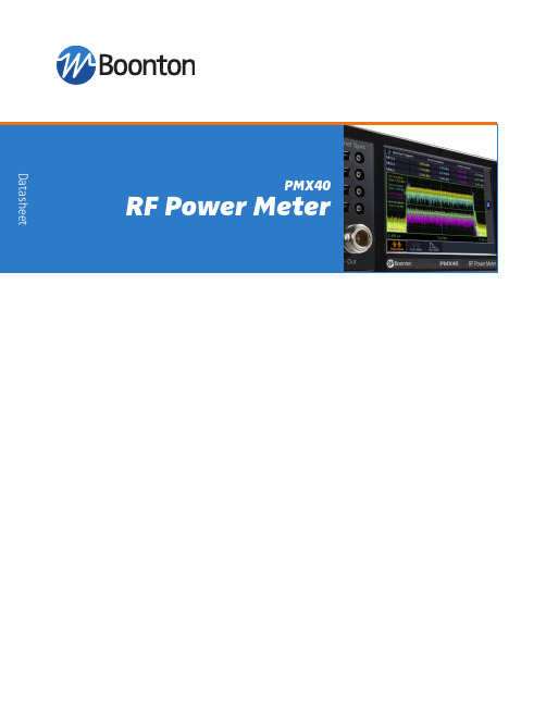
The PMX40 provides design engineers and technicians the utility of traditional benchtop instrument, the flexibility and performance of modern USB RF power sensors, and the simplicity of a multi-touch display built with Boonton award-winning technology.As a benchtop meter, the PMX40 provides a standalone solution for capturing, displaying, and analyzing peak and average RF power in both the time and statistical domains through an intuitive, multi-touch touchscreen display.The PMX40 Power Meter utilizes up to four RTP and CPS families of USB RF power sensors with industry- leading performance and capabilities either independently or for synchronized multi-channel measurements of CW, modulated, and pulsed signals.Providing the ultimate flexibility, the PMX40 sensors can be disconnected and independently used as standalone instruments.Key Features• Capture/display/analyze peak and average power• Frequency range from 4 kHz to 40 GHz• Industry-leading video bandwidth (195 MHz) and rise time (3 ns)• Industry-leading 100,000 measurements per second• Industry-leading 100 ps time resolution• Synchronous multi-channel measurements (up to 4 channels)• Sensors can be used as standalone instruments PMX40 RF Power MeterPulsed ModeAnalysis of fast-rising single pulses or pulses with short pulserepetition intervals (PRIs) requires an instrument with sophisticated trigger and data acquisition capability. Within Pulsed Mode, more than 16 pulse parameters can be measured.Continuous ModeFor simple, intuitive measurements of repetitive waveforms, the PMX40 Continuous Mode of operation provides a numeric display of average, maximum and minimum signal powers.Statistical ModeIn Statistical Mode, the PMX40 plots the Complementary Cumulative Distribution Function (CCDF). The CCDF plot shows the rate of occurrence of a specific crest factor for signals, such as those used in 5G, 4G/LTE, and Wi-Fi applications.PMX40 RF Power Meter – Front PanelConnect up to 4 USB sensors for multi-channel measurements.Multi-touch display with intuitive user interface.One touch to quickly access presets and favorite functions.Sync ports to source or receive triggers for timing and synchronization.Test source to verify sensor operation.The PMX40’s intuitive, multi-touch display enables fast configuration of up to four sensors as well as easy access to measurement and analysis tools, providing a standalone solution for capturing, displaying, and analyzing peak and average RF power in both the time and statistical domains. The meter also incorporates a test source to verify sensor operation.High-Performance and Versatile USB Power Sensors• Real-Time Power Processing™ technology with virtually zero measurement latency • 100,000 measurements per second • 80 dB dynamic range• Synchronized multi-channel measurementsAll RTP Real-Time Power SensorsThe Boonton PMX40 Power Meter utilizes Boonton RTP and CPS families of USB RF power sensors with indus-try leading performance and capabilities. All RTP sensors incorporate the unique Boonton Real-Time Power Processing™ technology, which virtually eliminates gaps in measurement suffered by other power sensors and enables industry best measurement speeds. In terms of RF performance, the RTP5000 series Real-Time Peak Power Sensors are the fastest responding sensors with 3 ns rise times and 195 MHz of video bandwidth. The RTP4000 series Real-Time True Average Power Sensors enable the lowest frequency measurements for diode-based average power measuring sensors and can make accurate measurements virtually independent of signal modulation bandwidth. CPS sensors offer flexible connectivity and performance leadership at anexcellent price point.Real-Time Power Processing™Boonton Real-Time Power Processing 1 dramatically reduces the total cycle time for acquiring and processing power measurement samples. By combining a dedicated acquisition engine, hardware trigger, integrated sample buffer, and a real-time optimized parallel processing architecture, Real-Time Power Processing™ performs most of the sweep processing steps simultaneously, beginning immediately after the trigger instead of waiting for the end of the acquisition cycle.The advantages of the Real-Time Power Processing technique are that key processing steps take place in parallel and keep pace with the signal acquisition. With no added computational overhead to prolong the sweep cycle, the sample buffer cannot overflow. As a result, there is no need to halt acquisition for trace processing. This means gap-free signal acquisition virtually guarantees that intermittent signal phenomena such as transients or dropouts will be reliably captured and analyzed.1RTPP is available within the RTP500 and RTP4000 sensors.Software FeaturesMeasurement Buffer ModeThe RTP series Measurement Buffer Mode is a remote control function that works in conjunction with Real-Time Power Processing to provide only therelevant burst or pulse information, eliminating the need to download and post-process large sample buffers. As a result, users can collect and analyze measurements from a virtually unlimited number of consecutive pulses or events without gaps. A wide variety of parameters can be calculated and plotted, such as duty cycle, pulse repetition rate, pulse width variation, and pulse jitter. In addition, anomalies,such as dropouts, can be identified.Dropouts, such as those shown left, are the sorts of events often missed by conventional power meters due to the acquisition gaps while processing takes place.Example seven pulse waveform.Measurement buffer data returned for waveform in above.Wi-Fi and Wireless Communication Signal AnalysisCharacterization and compliance testing of Wi-Fi and LTE chipsets and devices involves significant challenges for design and test engineers. With multiple-input, multiple-output (MIMO) architectures and channel bandwidths up to 160 MHz, testing is complex, especially when measuring RF power per channel and time alignment between channels. The PMX40 enables packet power measurements to be performed independently on multiple synchronous or asynchronous transmit chains with a common timebase shared among sensors.Use markers to define a portion of the waveform on which to make measurements. “Between Marker” measurements are ideal for monitoring specific portions of a packet over long intervals.Video bandwidth (VBW) describes the ability of a power sensor to track peak (envelope) power. Insufficient VBW will result in errant envelope and average power measurements. The PMX40 offers the widest video bandwidth (195 MHz) making it ideal for measuring 80 MHz, 100 MHz, and 160MHz channels.By comparing the peak-to-average power ratio, or crest factor (CF), of input and output signals of an RF transmission chain, engineers can assess circuit linearity. Additional insight can be provided with the PMX40 statistical mode Complementary Cumulative Distribution Function (CCDF) plot displaying the rate of occurrence of a specific CF. As an amplifier output compresses, the CF will reduce and the CCDF plot will move left.Indication of amplifier output compressionCrest FactorSecondary Surveillance Radar (SSR)Design, verification, troubleshooting and maintenance of secondary surveillanceradar (e.g. IFF-based radar) has never been more demanding.Proper design and operation of SSR systems is critical to the safety and security of aviation. The PMX40 can b e u sed t o easily a nd accurately capture SSR waveforms. Markers enable measurements on specific portions of the waveform.Industry-leading rise time (<3 ns) enables characterization of the most demanding radar signals.Utilize the superior 100 ps time resolution to zoom and uncover signal characteristics that might otherwise be missed.Key Features and Functionality• Data displayed as numerical meter or waveform trace • Statistical analysis with CCDF plot• Multiple marker measurements, including between marker data and marker ratios • Automated measurements; e.g., 16 automated pulse measurements • Export measurement data in .csv or .pdf formats • Up to 8 simultaneous power measurement channels• Simulation mode available to preview functionality when a sensor is not availableKey Features and Functionality• Large numeric readout and/or analog meter display • Zoom and pan through data logging strip chart• Quickly set frequency, aperture (averaging) and offset values all from the main screen• Calculates ratios between sensor measurements • Control up to 8 sensors at once• Simulation mode available to preview functionality when a sensor is not availableSensor SoftwarePower Viewer – Simple and Intuitive Measurement Software(for standalone operation of the CPS2000 Series of sensors)Power Viewer is a complimentary PC-based software package for CPS2008 sensor control, measurement configuration, and analysis. It includes USB drivers, remote control API, firmware updater and virtual instrument application.(for standalone operation of the RTP4000 and RTP5000 series of sensors)Power Analyzer is a complimentary PC-Based software package for RTP5000 and RTP4000 sensor control, measurement configuration, and advanced analysis. It includes USB drivers, remote control API, firmwareupdater and virtual instrument application.Power Analyzer - Advanced Measurement and Analysis SoftwareSensor SpecificationsRTP5006RTP5318 RF Frequency Range50 MHz to 6 GHz50 MHz to 18 GHz Dynamic RangeSpecificationsChannels Up to 4 Sensors RTP5000 SeriesRTP4000 SeriesCPS2000 Series Display5-inch WVGA multi-touch display with intuitive graphical user interfaceDisplay Modes Trace (power vs time)Statistical measurements Meter (numeric display)CCDFAutomatic measurements (pulse, statistical, and markers measurements)Marker Measurements (in Trace View)Markers (vertical cursors)Marker IndependentlyInterval Between MarkersPair of MarkersSettable in time relative to the trigger positionAvg, Min and Max Power at a specified time offsetAvg, Min and Max Power over the defined intervalRatio of power values at each markerPulse Mode – Automatic Measurements Pulse rise-timePulse widthPulse periodPulse duty cyclePulse peakPulse overshootTop level powerEdge delayPulse fall-timePulse off-timePulse repetition frequencyWaveform averagePulse averagePulse droopBottom level powerPulse edge skew between channelsStatistical Mode –Automatic Measurements Peak powerMinimum powerDynamic rangeCrest factor at cursorAverage powerPeak to average ratioPercent at cursorCrest factor at various percentsTrigger Synchronization*ModeSourceInternal Level RangeExternal Level RangeSlopeHold-off, Min Pulse Width, Max Trigger RateAmong RTP Series(internal trig distribution)Normal, Auto, Auto Pk-to-Pk, Free Run Any connected RTP Series sensor (via SMB’s) or rearpanel external trigger -40 dBm to +20 dBm (sensor dependent)±5 volts or TTL+ or -Sensor and timebase dependentTime Base Time Base Resolution, Range, AccuracyTime Base DisplayTrigger Delay RangeTrigger Delay ResolutionSensor dependent Sweeping or Roll Mode Sensor dependent0.02 divisionsSpecifications, ContinuedInputs/Outputs (front panel)USB with SMB trigger port Test Source50 MHz(optional rear panel placement)Inputs/Outputs (rear panel)LANUSB with SMB trigger portWireless Telecom Group Inc. 25 Eastmans Rd Parsippany, NJ United StatesTel: +1 973 386 9696 Fax: +1 973 386 9191 © Copyright 2020 All rights reserved.B/PMX40/0520/ENNote: Specifications, terms and conditions are subject to change without prior notice.PMX40RF Power Meter (includes 2 active channels)OptionsPMX40-4CH PMX40-GPIB PMX40-RTSAdds 2 Active Channels (for a total of 4)GPIB Control (internally installed)Moves Test Source output to the rear panelIncluded AccessoriesInformation Card (provides information on where to download the latest manual, software, utilities)Optional AccessoriesPMX40-RMK PMX40-TCASEFull-width 19” Rack Mount Kit (includes handles & hardware for mounting one or two meters)Transit case, hold the PMX40 and up to 4 sensorsRF Power SensorsCPS2008RTP4006RTP4106RTP4018*RTP4040*RTP5006RTP5318RTP5518RTP5340RTP5540True Average Connected Power Sensor Real-Time True Average Power Sensor Real-Time True Average Power Sensor Real-Time True Average Power Sensor Real-Time True Average Power Sensor Real-Time Peak Power Sensor Real-Time Peak Power Sensor Real-Time Peak Power Sensor Real-Time Peak Power Sensor Real-Time Peak Power Sensor50 MHz to 8 GHz 10 MHz to 6 GHz 4 kHz to 6 GHz 10 MHz to 18 GHz 10 MHz to 40 GHz 50 MHz to 6 GHz 50 MHz to 18 GHz 50 MHz to 18 GHz 50 MHz to 40 GHz 50 MHz to 40 GHzIncluded AccessoriesInformation Card (provides information on where to download the latest manual, software, utilities)0.9 m BNC (m) to SMB (m) cable (RTP sensors)0.9 m SMB (m) to SMB (m) cable (RTP sensors)1.8 m USB A (m) to USB B (m) locking SeaLATCH cable (RTP sensors)1.6 m USB A (m) to USB B (m) cable (CPS sensors)Ordering Information*RTP4018 and RTP4040 are currently in development. Specifications and performance subject to change。

ac: Alternating current; an electric current that reverses its direction at regularly recurring intervals.Accuracy: The closeness of an indication or reading of a measurement device to the actual value of the quantity being measured. Usually expressed as ± percent of full scale output or reading.Acoustics: The degree of sound. The nature, cause, and phenomena of the vibrations of elastic bodies; which vibrations create compressional waves or wave fronts which are transmitted through various media, such as air, water, wood, steel, etc.Adapter: A mechanism or device for attaching non-mating parts.ADC: Analog-to-Digital Converter: an electronic device which converts analog signals to an equivalent digital form, in either a binary code or a binary-coded-decimal code. When used for dynamic waveforms, the sampling rate must be high to prevent aliasing errors from occurring. Ambient Compensation: The design of an instrument such that changes in ambient temperature do not affect the readings of the instrument.Ambient Conditions: The conditions around the transducer (pressure, temperature, etc.).Ambient Pressure: Pressure of the air surrounding a transducer.Ambient Temperature: The average or mean temperature of the surrounding air which comes in contact with the equipment and instruments under test.Ampere (amp): A unit used to define the rate of flow of electricity (current) in a circuit; units are one coulomb (6.28 x 10¹⁸ electronics) per second.Amplitude: A measurement of the distance from the highest to the lowest excursion of motion, as in the case of mechanical body in oscillation or the peak-to-peak swing of an electrical waveform. Analog Output: A voltage or current signal that is a continuous function of the measured parameter.Analog-to-Digital Converter (A/D or ADC): A device or circuit that outputs a binary number corresponding to an analog signal level at the input.ATC: Automatic temperature compensation.Background Noise: The total noise floor from all sources of interference in a measurement system, independent of the presence of a data signal.Bandwidth: A symmetrical region around the set point in which proportional control occurs.Baud: A unit of data transmission speed equal to the number of bits (or signal events) per second; 300 baud = 300 bits per second.Bearing: A part which supports a journal and in which a journal revolves.Beta Ratio: The ratio of the diameter of a pipeline constriction to the unconstricted pipe diameter. BNC: A quick disconnect electrical connector used to inter-connect and/or terminate coaxial cables. BTU: British thermal units. The quantity of thermal energy required to raise one pound of water at its maximum density, 1 degree F. One BTU is equivalent to .293 watt hours, or 252 calories. One kilowatt hour is equivalent to 3412 BTU.Bus: Parallel lines used to transfer signals between devices or components. Computers are often described by their bus structure (i.e., S-100, IBM PC).Calibration: The process of adjusting an instrument so that its reading can be correlated to the actual value being measured.Cavitation: The boiling of a liquid caused by a decrease in pressure rather than an increase in temperature.CE approval: CE marking is a declaration by the manufacturer that the product meets all the appropriate provisions of the relevant legislation implementing certain European Directives. The initials "CE" do not stand for any specific words but are a declaration by the manufacturer that his product meets the requirements of the applicable European Directive(s). Portaflow 330, 220A, 220B models manufactured in accordance with the following Directives and Standards: Directive2004/108/EC, Directive 2006/95/EC. BS EN 61010-1:2001, BS EN61326-1:2006, BS EN613626-2:2006.Centre of Gravity (Mass Centre): The centre of gravity of a body is that point in the body through which passes the resultant of weights of its component particles for all orientations of the body with respect to a uniform gravitational field.CFM: The volumetric flow rate of a liquid or gas in cubic feet per minute.Closeness of Control: Total temperature variation from a desired set point of system. Expressed as "closeness of control" is ±2°C or a system bandwidth with 4°C, also referred to as amplitude of deviation.Colour Code: The ANSI established colour code for thermocouple wires in the negative lead is always red. Colour Code for base metal thermocouples is yellow for Type K, black for Type J, purple for Type E and blue for Type T.Communication: Transmission and reception of data among data processing equipment and related peripherals.Compensated Connector: A connector made of thermocouple alloys used to connect thermocouple probes and wires.Compensation: An addition of specific materials or devices to counteract a known error.Confidence Level: The range (with a specified value of uncertainty, usually expressed in percent) within which the true value of a measured quantity exists.Connection Head: An enclosure attached to the end of a thermocouple which can be cast iron, aluminium or plastic within which the electrical connections are made.Convection: 1. The circulatory motion that occurs in a fluid at a non-uniform temperature owing to the variation of its density and the action of gravity. 2. The transfer of heat by this automatic circulation of fluid.CPS: Cycles per second; the rate or number of periodic events in one second, expressed in Hertz (Hz).Critical Damping: Critical damping is the smallest amount of damping at which a given system is able to respond to a step function without overshoot.Critical Speed: The rotational speed of the rotor or rotating element at which resonance occurs in the system.Damping: The reduction of vibratory movement through dissipation of energy. Types include viscous, coulomb, and solid.dB (Decibel): 20 times the log to the base 10 of the ratio of two voltages. Every 20 dBs correspond to a voltage ratio of 10, every 10 dBs to a voltage ratio of 3.162. For instance, a CMR of 120 dB provides voltage noise rejection of 1,000,000/1. An NMR of 70 dB provides voltage noise rejection of 3,162/1.DC: Direct current; an electric current flowing in one direction only and substantially constant in value.Dead Volume: The volume of the pressure port of a transducer at room temperature and ambient barometric pressure.Default: The value(s) or option(s) that are assumed during operation when not specified.Degree: An incremental value in the temperature scale, i.e., there are 100 degrees between the ice point and the boiling point of water in the Celsius scale and 180°F between the same two points in the Fahrenheit scale.Density: Mass per unit of volume of a substance. I.E.: grams/cu.cm. or pounds/cu.ft.Deviation: The difference between the value of the controlled variable and the value at which it is being controlled.Differential: For an on/off controller, it refers to the temperature difference between the temperature at which the controller turns heat off and the temperature at which the heat is turned back on. It is expressed in degrees.Digital Output: An output signal which represents the size of an input in the form of a series of discrete quantities.Digital-to-Analog Converter (D/A or DAC): A device or circuit to convert a digital value to an analog signal level.DIN (Deutsche Industrial Norm): A set of German standards recognized throughout the world. The 1/8 DIN standard for panel meters specifies an outer bezel dimension of 96 x 48 mm and a panel cutout of 92 x 45 mm.Doppler Technology: An acoustic pulse is reflected back to the sensor from particles or gases in the flowing liquid. The flow rate of any fluid can be measured as long as it contains air bubbles or solids. It is ideal for wastewater, slurries, sludge and most chemicals, acids, caustics and lubrication fluids.Drift: A change of a reading or a set point value over long periods due to several factors including change in ambient temperature, time, and line voltage.Duplex: Pertaining to simultaneous two-way independent data communication transmission in both direction. Same as "full duplex".Echo: To reflect received data to the sender. For example, keys depressed on a keyboard are usually echoed as characters displayed on the screen.Electrical Interference: Electrical noise induced upon the signal wires that obscures the wanted information signal.EMI: Electromagnetic interference.Emissivity: The ratio of energy emitted by an object to the energy emitted by a blackbody at the same temperature. The emissivity of an object depends upon its material and surface texture; a polished metal surface can have an emissivity around 0.2 and a piece of wood can have an emissivity around 0.95.End Point (Potentiometric): The apparent equivalence point of a titration at which a relatively large potential change is observed.Environmental Conditions: All conditions in which a transducer may be exposed during shipping, storage, handling, and operation.Error: The difference between the value indicated by the transducer and the true value of the measurand being sensed.Explosion-proof Enclosure: An enclosure that can withstand an explosion of gases within it and prevent the explosion of gases surrounding it due to sparks, flashes or the explosion of the container itself, and maintain an external temperature which will not ignite the surrounding gases.Exposed Junction: A form of construction of a thermocouple probe where the hot or measuring junction protrudes beyond the sheath material so as to be fully exposed to the medium being measured. This form of construction usually gives the fastest response time.Fahrenheit: A temperature scale defined by 32° at the ice point and 212° at the boiling point ofwater at sea level.Ferrule: A compressible tubular fitting that is compressed onto a probe inside a compression fitting to form a gas-tight seal.Field Balancing Equipment: An assembly of measuring instruments for performing balancing operations on assembled machinery which is not mounted in a balancing machine.Field of View: A volume in space defined by an angular cone extending from the focal plane of an instrument.File: A set of related records or data treated as a unit.Flow Rate: Actual speed or velocity of fluid movement.Flow: Travel of liquids in response to a force (i.e. pressure or gravity).FPM: Flow velocity in feet per minute.FPS: Flow velocity in feet per second.Freezing Point: The temperature at which the substance goes from the liquid phase to the solid phase.Frequency Output: An output in the form of frequency which varies as a function of the applied input.Frequency, Natural: The frequency of free (not forced) oscillations of the sensing element of a fully assembled transducer.Frequency: The number of cycles over a specified time period over which an event occurs. The reciprocal is called the period.Full Scale Output: The algebraic difference between the minimum output and maximum output. GPH: Volumetric flow rate in gallons per hour.GPM: Volumetric flow rate in gallons per minute.Ground: 1. The electrical neutral line having the same potential as the surrounding earth. 2. The negative side of DC power supply. 3. Reference point for an electrical system.Grounded Junction: A form of construction of a thermocouple probe where the hot or measuring junction is in electrical contact with the sheath material so that the sheath and thermocouple will have the same electrical potential.Handshake: An interface procedure that is based on status/data signals that assure orderly data transfer as opposed to asynchronous exchange.Hardware: The electrical, mechanical and electromechanical equipment and parts associated with acomputing system,Heat Sink: 1. Thermodynamic. A body which can absorb thermal energy. 2. Practical. A finned piece of metal used to dissipate the heat of solid state components mounted on it.Heat Transfer: The process of thermal energy flowing from a body of high energy to a body of low energy. Means of transfer are: conduction; the two bodies contact. Convection; a form of conduction where the two bodies in contact are of different phases, i.e. solid and gas. Radiation: all bodies emit infrared radiation.Heat Treating: A process for treating metals where heating to a specific temperature and cooling at a specific rate changes the properties of the metal.Heat: Thermal energy. Heat is expressed in units of calories or BTU's.Hertz (Hz): Units in which frequency is expressed. Synonymous with cycles per second.ID: Inside diameterInfrared: An area in the electromagnetic spectrum extending beyond red light from 760 nanometers to 1000 microns (106 nm). It is the form of radiation used for making non-contact temperature measurements.Insulated Junction: See Ungrounded JunctionInsulation Resistance: The resistance measured between two insulated points on a transducer when a specific dc voltage is applied at room temperature.Interchangeability Error: A measurement error that can occur if two or more probes are used to make the same measurement. It is caused by a slight variation in characteristics of different probes. Interface: The means by which two systems or devices are connected and interact with each other. Intrinsically Safe: An instrument which will not produce any spark or thermal effects under normal or abnormal.IP Rating: (or "Ingress Protection") ratings are defined in international standard EN 60529 (British BS EN 60529:1992, European IEC 60509:1989). They are used to define levels of sealing effectiveness of electrical enclosures against intrusion from foreign bodies (tools, dirt etc) and moisture.IP66: First digit is the intrusion protection, in this case 6 is totally dust tight. Second digit is moisture protection, in this instance protection against string water jets and waves.IP67: Total dust ingress protection and protected against temporary immersion between 15cm and 1m depth.Isolation: The reduction of the capacity of a system to respond to an external force by use of resilient isolating materials.Joule: The basic unit of thermal energy.Junction: The point in a thermocouple where the two dissimilar metals are joined.Kelvin: Symbol K. The unit of absolute or thermodynamic temperature scale based upon the Celsius scale with 100 units between the ice point and boiling point of water. 0°C = 273.15K (there is no degree (°) symbol used with the Kelvin scale).Kilowatt (kw): Equivalent to 1000 watts.Kilowatt Hour (kwh): 1000 watthours. Kilovolt amperes (kva): 1000 volt amps.Kinetic Energy: Energy associated with mass in motion, i.e., 1/2 rV2 where r is the density of the moving mass and V is its velocity.Laminar Flow: Streamlined flow of a fluid where viscous forces are more significant than inertial forces, generally below a Reynolds number of 2000.Leakage Rate: The maximum rate at which a fluid is permitted or determined to leak through a seal. The type of fluid, the differential Limits of Error: A tolerance band for the thermal electric response of thermocouple wire expressed in degrees or percentage defined by ANSI specification MC-96.1 (1975).Life Cycle: The minimum number of pressure cycles the transducer can endure and still remain within a specified tolerance.Linearity: The closeness of a calibration curve to a specified straight line. Linearity is expressed as the maximum deviation of any calibration point on a specified straight line during any one calibration cycle.Load Impedance: The impedance presented to the output terminals of a transducer by the associated external circuitry.Load: The electrical demand of a process expressed as power (watts), current (amps) or resistance (ohms).M: Mega; one million. When referring to memory capacity, two to the twentieth power (1,048,576 in decimal notation).Mass Flow Rate: Volumetric flowrate times density, i.e. pounds per hour or kilograms per minute. Maximum Operating Temperature: The maximum temperature at which an instrument or sensor can be safely operated.Maximum Power Rating: The maximum power in watts that a device can safely handle.Mean Temperature: The average of the maximum and minimum temperature of a process equilibrium.Method of Correction: A procedure whereby the mass distribution of a rotor is adjusted to reduce unbalance, or vibration due to unbalance, to an acceptable value. Corrections are usually made byadding material to, or removing it from, the rotor.Mica: A transparent mineral used as window material in high-temperature ovens.Microamp: One millionth of an ampere, 10-6 amps, µA.Micron: One millionth of a meter, 10-6 meters.Mil: One thousandth of an inch (.001").Millimeter: One thousandth of a meter, symbol mm.NB: Nominal Bore.NEMA-4: A standard from the National Electrical Manufacturers Association, which defines enclosures intended for indoor or outdoor use primarily to provide a degree of protection against windblown dust and rain, splashing water, and hose-directed water.NEMA-7: A standard from the National Electrical Manufacturers Association, which defines explosion-proof enclosures for use in locations classified as Class I, Groups A, B, C or D, as specified in the National Electrical Code.NEMA-12: A standard from the National Electrical Manufacturers Association, which defines enclosures with protection against dirt, dust, splashes by non-corrosive liquids, and salt spray. Noise: An unwanted electrical interference on the signal wires.O.D.: Outside diameter.Offset: The difference in temperature between the set point and the actual process temperature. Also, referred to as droop.Output Impedance: The resistance as measured on the output terminals of a pressure transducer. Output Noise: The RMS, peak-to-peak (as specified) ac component of a transducer's dc output in the absence of a measurand variation.Output: The electrical signal which is produced by an applied input to the transducer.Parity: A technique for testing transmitting data. Typically, a binary digit is added to the data to make the sum of all the digits of the binary data either always even (even parity) or always odd (odd parity).Phase: A time based relationship between a periodic function and a reference. In electricity, it is expressed in angular degrees to describe the voltage or current relationship of two alternating waveforms.Polypropylene: A polymer of propylene used as a thermoplastic moulding material. Doesn't soak up water, making it ideal for uses where it will be constantly subject to moisture.PortaGraph Software: Portagraph II is a software application specifically written for use with Micronics flowmeters which simplifies the downloading and viewing of the instum ent’s logged data. Data may also be viewed in text format or exported to Excel for more detailed analysis. Also allows real time monitoring, where measured data is automatically captured sample by sample and displayed in either graph or data table format. Data logged in one set of units can quickly be converted to another set if required.Positive Temperature Coefficient: An increase in resistance due to an increase in temperature.Potential Energy: Energy related to the position or height above a place to which fluid could possibly flow.Power Supply: A separate unit or part of a circuit that supplies power to the rest of the circuit or to a system.PPM: Abbreviation for "parts per million," sometimes used to express temperature coefficients. For instance, 100 ppm is identical to 0.01%.Primary Device: Part of a flowmeter which is mounted internally or externally to the fluid conduit and produces a signal corresponding to the flowrate and from which the flow may be determined.Probe: A generic term that is used to describe many types of temperature sensors.Process Meter: A panel meter with sizeable zero and span adjustment capabilities, which can be scaled for readout in engineering units for signals such as 4-20 mA, 10-50 mA and 1-5 V.Range: Those values over which a transducer is intended to measure, specified by its upper and lower limits.Rangeability: The ratio of the maximum flowrate to the minimum flowrate of a meter.Rankine (°R): An absolute temperature scale based upon the Fahrenheit scale with 180° between the ice point and boiling point of water. 459.67°R = 0°F.Real Time: The time interval over which the system temperature is sampled for the derivative function.Reference Mark: Any diagnostic point or mark which can be used to relate a position during rotation of a part to its location when stopped.Relay (Mechanical): An electromechanical device that completes or interrupts a circuit by physically moving electrical contacts into contact with each other.Relay (Solid State): A solid state switching device which completes or interrupts a circuit electrically with no moving parts.Remote: Not hard-wired; communicating via switched lines, such as telephone lines. Usually refers to peripheral devices that are located a site away from the CPU.Repeatability: The ability of a transducer to reproduce output readings when the same measured value is applied to it consecutively, under the same conditions, and in the same direction.Repeatability is expressed as the maximum difference between output readings.Residual (Final) Unbalance: Residual unbalance is that unbalance of any kind that remains after balancing.Resistance: The resistance to the flow of electric current measured in ohms (1/2) for a conductor. Resistance is function of diameter, resistivity (an intrinsic property of the material) and length.Reynolds Number: The ratio of inertial and viscous forces in a fluid defined by the formula Re = rVD/µ, where: r = Density of fluid, µ = Viscosity in centipoise (CP), V = Velocity, and D = Inside diameter of pipe.RFI: Radio frequency interference.Secondary Device: A part of the flowmeter which receives a signal proportional to the flowrate, from the primary device, and displays, records and/or transmits the signal.Sensing Element: That part of the transducer which reacts directly in response to the input.Sensitivity Shift: A change in slope of the calibration curve due to a change in sensitivity.Sensitivity: The minimum change in input signal to which an instrument can respond.SI: System Internationale. The name given to the standard metric system of units.Signal: An electrical transmittance (either input or output) that conveys information.Spectrum: The resolving of overall vibration into amplitude components as a function of frequency.Stability: The quality of an instrument or sensor to maintain a consistent output when a constant input is applied.Temperature Error: The maximum change in output, at any measure and value within the specified range, when the transducer temperature is changed from room temperature to specified temperature extremes.Temperature Range, Compensated: The range of ambient temperatures within which all tolerances specified for Thermal Zero Shift and Thermal Sensitivity Shift are applicable (temperature error).Thermal Coefficient of Resistance: The change in resistance of a semiconductor per unit change in temperature over a specific range of temperature.Thermal Conductivity: The property of a material to conduct heat in the form of thermal energy.Thermocouple: The junction of two dissimilar metals which has a voltage output proportional to the difference in temperature between the hot junction and the lead wires (cold junction) Thomson Effect: When current flows through a conductor within a thermal gradient, a reversible absorption or evolution of heat will occur in the conductor at the gradient boundaries.Time of Flight (TOF): describes a variety of methods that measure the time that it takes for an object, particle or acoustic, electromagnetic or other wave to travel a distance through a medium. This measurement can be used for a time standard as a way to measure velocity or path length through a given medium, or as a way to learn about the particle or medium (such as composition or flow rate).Transducer Vibration: Generally, any device which converts movement, either shock or steady state vibration, into an electrical signal proportional to the movement; a sensor.Transducer: A device (or medium) that converts energy from one form to another. The term is generally applied to devices that take physical phenomenon (pressure, temperature, humidity, flow, etc.) and convert it to an electrical signal.Transient Vibration: A temporary vibration or movement of a mechanical system.Transit Time: A typical transit-time flow measurement system utilizes two ultrasonic transducers that function as both ultrasonic transmitter and receiver. The flow meter operates by alternately transmitting and receiving a burst of sound energy between the two transducers and measuring the transit time that it takes for sound to travel between the two transducers. The difference in the transit time measured is directly and exactly related to the velocity of the liquid in the pipe.Transitional Flow: Flow between laminar and turbulent flow, usually between a pipe Reynolds number of 2000 and 4000.Transmitter (Two-Wire): 1. A device which is used to transmit data from a sensor via a two-wire current loop. The loop has an external power supply and the transmitter acts as a variable resistor with respect to its input signal. 2. A device which translates the low level output of a sensor or transducer to a higher level signal suitable for transmission to a site where it can be further processed.Turbulent Flow: When forces due to inertia are more significant than forces due to viscosity. This typically occurs with a Reynolds number in excess of 4000.Union: A form of pipe fitting where two extension pipes are joined at a separable coupling.Vacuum: Any pressure less than atmospheric pressure.Velocity: The time rate of change of displacement; dx/dt.Vibration Error Band: The error recorded in output of a transducer when subjected to a given set of amplitudes and frequencies.Vibration Error: The maximum change in output of a transducer when a specific amplitude and range of frequencies are applied to a specific axis at room temperature.Viscosity: The inherent resistance of a substance to flow.Volt: The (electrical) potential difference between two points in a circuit. The fundamental unit is derived as work per unit charge-(V = W/Q). One volt is the potential difference required to moveone coulomb of charge between two points in a circuit while using one joule of energy.Voltage: An electrical potential which can be measured in volts.Volume Flow Rate: Calculated using the area of the full closed conduit and the average fluid velocity in the form, Q = V x A, to arrive at the total volume quantity of flow. Q = volumetric flowrate, V = average fluid velocity, and A = cross sectional area of the pipe.Watt Density: The watts emanating from each square inch of heated surface area of a heater. Expressed in units of watts per square inch.Working Standard: A standard of unit measurement calibrated from either a primary or secondary standard which is used to calibrate other devices or make comparison measurements.Zero Offset: 1. The difference expressed in degrees between true zero and an indication given by a measuring instrument. 2. See Zero Suppression。

固化剂硫醇当量的测定方法Determining the equivalent amount of thiol in a curing agent is crucial in various industries such as pharmaceuticals, cosmetics, and food. The thiol equivalent is a measure of the reactive functionality of the curing agent, and it is essential to accurately determine this value for quality control and formulation purposes. There are several methods for determining the thiol equivalent of a curing agent, and each method has its advantages and limitations.确定固化剂硫醇当量在制药、化妆品和食品等各个行业中非常关键。
硫醇当量是固化剂反应功能性的衡量标准,准确测定这个数值对于质量控制和配方设计至关重要。
有几种方法可以确定固化剂硫醇当量,每种方法都有其优点和局限性。
One common method for determining the thiol equivalent of a curing agent is titration with a standard solution of a known concentration. In this method, a known amount of the curing agent is reacted with a standard solution of a chemical reagent, and the amount of reagent consumed is used to calculate the thiol equivalent. This method is relatively simple and can provide accurateresults, but it requires careful handling of the reagents and precise measurements.一种常用的确定固化剂硫醇当量的方法是使用已知浓度的标准溶液进行滴定。

The Doherty Power Amplifier The current wireless communication systems have made significant progress toward increased bandwidth and number of carriers for high-data-rate applications. Memory effects, however, make it very difficult to design a high-power amplifier with a wide instantaneous bandwidth. In addition to bandwidth concerns, the instantaneous transmit powers of the wireless communication systems, such as CDMA-2000, wide-band code division multiple access (WCDMA), orthogonal frequency division multiplexity (OFDM) and so on, vary widely and rapidly, carrying high peak-to-average ratio (PAR) signals. The base station power amplifiers for the systems require a high linearity to amplify the high PAR signal source without distortion. To satisfy linearity requirements, the power amplifiers are usually biased at class A or AB mode and must operate at a large amount of back-off from the peak output power. Another requirement of the base station power amplifier for the modern wireless communication systems is high efficiency. As the communication systems are reduced in both size and cost, the cooling system should be simple and small, requiring a power amplifier with high efficiency. Because the base station power amplifiers have a low efficiency due to the back-off operation, efficiency enhancement techniques become very important. The design technique of the base stationpower amplifiers with high efficiency and linearity across a wide instantaneous bandwidth has become a hot issue.In this article, we show that the Doherty amplifier iscapable of delivering the stringent requirements of the base station power amplifiers. We explain the operation principles, including both linearity and efficiency improvements, and the basic circuit configuration of the amplifier. Advanced design methods to operate across wide bandwidth and improve the linearity are also described. For verification, the Doherty amplifier is implemented using laterally diffused metal oxide semiconductor (LDMOS) transistors and measured using a WCDMA 4FA signal. These results show that the Doherty amplifier is a promising candidate for base station power amplifiers with wide bandwidth, high efficiency, and linearity.Doherty Amplifier OperationFigure1. (a)Operational diagram of the Doherty amplifier.(b) Fundamental currents. (c) Load impedances.The Doherty amplifier was first proposed by W.H. Doherty in 1936. The original Doherty amplifier consisted of two tube amplifiers and an impedance inverting network. The efficiency of an RF power amplifier is increased using the RF Doherty amplifier technique, as described in detail in . This amplifier consisted of a carrier amplifier and a peaking amplifier. The output load is connected to the carrier amplifier through an impedance inverter (a quarter-wave transmission line) and directly to the peaking amplifier. Figure 1(a) shows an operational diagram toanalyze the Doherty amplifier circuit. Two current sources represent the amplifiers. It is assumed that each current source is linearly proportional to the input voltage signal, operating as a class AB or class B amplifier with harmonic short circuits after it is turned on, and the efficiency analysis can be carried out using the fundamental and dc components only. As shown in Figure 1(b), the peaking amplifier turns on at one-half the maximum input voltage.The Doherty amplifier technique is based on the load impedance change of each amplifier, referred to as load modulation, according to the input power level. Figure 1(b) shows the fundamental currents from the amplifiers. The load impedances of two amplifiers are given bywhere ZL is the load impedance of the Doherty amplifier; IC and IP represent the fundamental currents of the carrier and peaking amplifiers, respectively; and ZC and ZP are the output load impedances of the carrier and peaking amplifiers, respectively, and are depicted in Figure 1(c).In the low-power region (0 ∼Vin, max/2), the peaking amplifier remains in the cut-off state, and the load impedance of the carrier amplifier is two times larger than that of the conventional amplifier. Thus, the carrier amplifier reaches the saturationstate at the input voltage(Vin, max)/2 since the maximum fundamental current swing is half and the maximum voltage swing reaches Vdc. As a result, the maximum power level is half of the carrier amplifier’s allowable power level (a quarter of the total maximum power or 6 dB down from the total maximum power), and the efficiency of the amplifier is equal to the maximum efficiency of the carrier amplifier as shown in Figure 2.In the high-power region (Vin, max/2 ∼Vin, max), where the peaking amplifier is conducting, the current level of the peaking amplifier plays an important role in determining the load modulation of the Doherty amplifier [see (1) and (2)]. Assuming that gm of the peaking amplifier is twice as large as that of the carrier amplifier, the current and voltage swings of the peaking amplifier increase in proportion to the input voltage level and the voltage swing reaches the maximum voltage swing of Vdc only at the maximum input voltage. The load impedance of the carrier amplifier varies from 2Zopt to Zopt, and the peaking amplifier varies from ∞ to Zopt according to the input voltage level as shown in Figure 1(c). The efficiency of the Doherty amplifier at the maximum input voltage is equal to the maximum efficiency of the amplifiers. When the peaking amplifier is the same size as the carrier amplifier, which is normally the case, gm of the two amplifiers are identical and the peaking amplifier can not be fullyturned on, so the powerperformance is degraded [4].From thebasic operation principle, we have exploredthe Doherty amplifier, which provides higher efficiency over whole power ranges compared to the conventional class AB amplifiers. The resulting Doherty amplifiercan solve the problem of maintaining a high efficiencyfor a large PAR signal.Linearity of the Doherty AmplifierThe linearity of the Doherty amplifier is more complicated than that of a class AB amplifier. The class AB biased carrier amplifier has a load impedance at the low power level that is twice as large and the high impedance of the carrier amplifier compensates the low gain characteristic due to the input power division. At high power levels, the two amplifiers generate full power using normal load impedances, equalizing the power gain. Additionally, in the low-power region, the linearity of the amplifier is entirely determined by the carrier amplifier. Therefore, the carrier amplifier should be highly linear even though the load impedance is highAt a high power level, linearity of the amplifier is improved by the harmonic cancellation from the two amplifiers using appropriate gate biases. Figure 3 shows the third-order harmonic generation coefficient gm3 of an LDMOS transistor and the bias points of the two amplifiers. In terms of gain characteristics of each amplifier, a late gain expansion of the class C biased peaking amplifier compensates the gain compression of the classAB carrier amplifier. Thus, the Doherty amplifier, which is based on the load modulation technique, is capable of delivering more linear output power than a conventional class AB power amplifier. The third-order intermodulation (IM3) level from the carrier amplifier increases and the phase of the IM3 decreases because the gain of the carrier amplifier is compressed. In contrast, when the gain of the peaking amplifier is expanded, both the IM3 level and phase increase. To cancel out the IM3s from the two amplifiers, the components must be 180◦out of phase with the same amplitudes. Therefore, the peaking amplifier should be designed appropriately to cancel the harmonics of the carrier amplifier..The Circuit Configuration of Doherty AmplifierFigure 4 shows a schematic diagram of the fully matched microwave Doherty amplifier with offset transmission lines at the output circuits [5]. The carrier and peaking amplifiers have input/output matching circuits, which transform from the input impedances of the devices to 50 and from the optimum load impedance Zopt of the devices to 50 , respectively. The additional offset transmission lines with characteristic impedance of 50 are connected after the matching circuits of the carrier and peaking amplifiers. In the low-power region, the phase adjustments of the offset lines cause the peaking amplifier to be open-circuited and the characteristic load impedance of the carrier amplifier is doubled to 2Ro by a quarterwave impedancetransformer. This is illustrated in Figure 5(a) and (b). The offset line of the carrier amplifier varies from Zopt to 2Zopt for the proper load modulation as shown in Figure 5(a). Figure 5(b) illustrates that the offset line of the peaking amplifier adjusts to the high impedance so that it prevents power leakage. Figure 5(c) shows the appropriate transformations on a Smith chart to determine the offset line length of each amplifier. The lines do not affect the overall matching condition and load modulation because they are matched to the characteristic impedance of 50 . The Doherty output combining circuit consists of a quarter-wave transmission line with the characteristic impedance of 50 and a quarter-wave transmission line that transforms from 50 to 25 to determine the load impedance of the output combining circuit. Aphase delay line is needed at the input of the peaking amplifier to adjust the same delay between the carrier and peaking amplifiers [6].The Doherty amplifier consists of a class AB biased carrier amplifier and a class C biased peaking amplifier. Due to the different biasing, the RF current from the amplifiersare different depending on the input drive level. The asymmetric powers are combined by the Doherty operation through a quarter-wave impedance converter.Advanced Design Methods for the Doherty AmplifierThe fundamental operation principles of a Doherty amplifierwere described in the previous section. We have seen that the advantages of the microwave Doherty amplifier are the simple circuit configuration and improved efficiency and linearity. In this section, we explain some typical issues with Doherty amplifiers and present proposed methods to address them.The Doherty amplifier for the base station system usually has two amplifiers with identical size devices, matching circuits, and input drives. Because the peaking amplifier is biased lower than the carrier amplifier, the current level of the peaking amplifier at the maximum input drive cannot reach the maximum allowable current level. Thus, the load impedances of both amplifiers can not be fully modulated to the optimized impedance, Zopt, and they are larger than the optimum values. As a result, the conventional Doherty amplifier is heavily saturated, and both linearity and power are degraded. It is difficult to improve the linearity of the Doherty amplifier across a wide bandwidth due to the memory effect. We propose the following three design methods for wide bandwidth, high linearity, and high power applications: 1) Uneven power drive, applying more power to the peaking amplifier, can open the peaking amplifier fully and modulate the load impedances optimally. Therefore, the amplifiers with uneven power drive operate more linear and produce more power than those with an identical input power drive. 2) Because of the improper load modulation, power matching circuits of bothamplifiers should be appropriately designed to have low load impedances for better linearity. Due to the low bias point of the peaking amplifier, the power matching circuit of the peaking amplifier should be designed to have lower load impedance than that of the carrier amplifier. Moreover, the matching circuits of both amplifiers should be individually optimized to enhance the IM cancellation over power ranges across the wide bandwidth.3) The bias circuit should be designed to minimize the memory effects. The linearizing techniques focused on harmonic cancellation such as Doherty amplifier and PD are restricted to a low cancellation limit because the memory effect brings about the different lower and upper spurious emissions. The bias circuit should not have any frequency dispersion of envelope impedance to minimize the memory effect. To reduce the memory effect, the bias circuit is optimized using a quarter-wave bias line and decoupling capacitors for each frequency. The tantalum capacitors are inserted within a quarterwave bias line for the short at the envelope frequencies. Additionally, the biases of both amplifiers are properly adjusted to maintain optimized linearity and efficiency.Bias Circuit Test to Reduce the Memory EffectsThe effects on the memory effect for different bandwidthsare ACLR or intermodulation distortion (IMD) asymmetry and bandwidth dependent adjacent channel leakage ratio (ACLR) or IMDcharacteristics. To reduce these effects or the memory effects, the load impedances of the bias circuit should be reduced to short the envelope frequency voltage component or maintained at the same value.We have tested several bias circuits to reduce the memory effect as shown in Figure 6. Figures 7 and 8 represent measurement results of load impedances corresponding to the bias circuit. Unfortunately, we cannot measure the envelope frequency load impedance (dc–20 MHz), but we have tested the load impedances at 100 MHz–5 GHz. We can analogize the envelope frequency load impedance of the bias circuit from these test results.The general bias circuit scheme of RF power amplifier is shown in Figure 6(b). From Figures 7 and 8, we have analogized that the envelope load impedances of the RF decoupling capacitor (10 pF) and envelope frequency decoupling capacitor (22 uF and 10 uF) were very small. Even though the envelope load impedances of this case are very small, the power amplifier has the serious memory effect.A cause of this result is that it is very difficult to short the envelope frequency voltage component because the load impedance of the high-power amplifier is very small. To minimize the memory effect, the load impedance of the bias circuit should be further reduced. Thus, we have proposed the bias circuit optimization method of the RF decoupling capacitor (10 pF) and envelope frequency decoupling capacitor [22 uF, 10 uF, and the tantalumcapacitor (1 uF) located within a quarter-wave bias circuit], and Figures 7(c) and 8(c) show more small envelope load impedances and lower load impedance variation than the general bias scheme at the low frequency. However, the impedance at RF is reduced by tantalum capacitor located within a quarter-wave bias line as shown in Figure 7(c). Thus, we need to optimize the bias circuit along with the matching circuit considering these effects. As a result, the proposed bias circuit optimization method can reduce the memory effect more efficiently than the conventional bias circuit method, and ACLR asymmetry is reduced.Implementation of the Doherty Amplifier and Measurement ResultsIn the previous section, we explained the basic Doherty operation and advanced design methods with uneven power drive, individually optimized matching, and bias circuit optimization. A2.14-GHz Doherty amplifier for the base station power amplifier is implemented using Freescale’s MRF5P21180 LDMOSFET. Figure 9 shows a photograph of the implemented Doherty amplifier applying the advanced methods. The uneven power drive is implemented using an Anaren’s 1A1305-5 (5 dB directional coupler) which delivers 4 dB more input power to the peaking amplifier than the carrier amplifier. The individual matching of the Doherty amplifier is further optimized to achieve high efficiency and linearity at 25 W (44 dBm) average output power. In the experiments, the suitableoffset line is 80.4◦, and the transformed output impedance of the peaking amplifier in the off state is 502 .Quiescent biases for the carrier amplifier and peaking amplifier are set to Vc = 3.938 V (1.1 A) and Vp = 1.713 V at Vdd = 27 V, respectively. We optimize the bias circuit to minimize the memory effect and improve the linearity and efficiency. For performance comparison, we also fabricated a class AB amplifier and Doherty amplifier with even power drive. The class AB amplifier represents a conventional base station power amplifier of the push-pull type. For specific comparison corresponding to uneven power drive, the Doherty amplifier with even drive is optimized using the individual matching and bias circuit to achieve linearity and efficiency as high as possible.Figure 10 shows the measured adjacent channel leakage ratio (ACLR) of the Doherty amplifier with uneven drive and class AB amplifier at offset 5 MHz for a 2.14-GHz forward link wideband code-division multiple-access (WCDMA) 4FA signal. The ACLR is improved by about 7 dB compared to the class AB amplifier at an output power of 44 dBm.Figure 11 shows the measured ACLR of the Doherty amplifiers for both even and uneven drives. In comparison with the even case, the Doherty amplifier with uneven power drive delivers significantly improved ACLR performance, by 3 dB at the average output power of 44 dBm.Figure 12 shows the measured ACLR performance of the uneven case as a function of the bias circuit optimization. The drain bias circuit incorporates a quarterwave line and several decoupling capacitors which consist of 10 pF for the RF and 22 uF, 10 uF, 1 uF, 1 nF, 150 nF for the envelope frequency. The tantalum capacitors (22 uF, 1 uF) located within a quarter-wave bias line are especially important to minimize the memory effect, even though the impedance at RF is reduced by these capacitors. Thus, we have optimized the bias circuit along with the matching circuit considering these effects. As a result, the bias circuit becomes an active matching circuit, and the difference in ACLR with the bias circuit optimization between lower and upper ACLR is reduced below 2 dB over all average output powers. Figure 13 shows the spectrum of the Doherty amplifier with uneven power drive at an average output power of 44 dBm according to the bias circuit optimization.Figure 14 shows the measured IMD3 of the Doherty amplifier with both even and uneven power drives for a two-tone signal. We measure a peak envelope power (PEP) using a two-tone signal with 1-MHz tone spacing. The PEP of the amplifier with uneven drive is improved by 15 W, from 165 to 180 W, compared to the even case. This result implies that the Doherty amplifier with uneven power drive generates full power from both amplifiers.Figure 15 shows drain efficiencies of the Doherty amplifierwith both even and uneven power drive and the class AB power amplifier for WCDMA 4 FA signal. The drain efficiency of the Doherty amplifier is significantly improved over the class AB amplifier.These results show clearly that the Doherty amplifier is far superior to the class AB amplifier. The Doherty amplifier with uneven power drive, based on the individually optimized matching circuit and the bias optimization, provides highly efficient and linear operation compared to the normal Doherty amplifier. We can also see that the proposed design method is very helpful in achieving the Doherty amplifier with high performance over a wide bandwidth.ConclusionsIn this article, we explained the basic Doherty operation principle, including both efficiency and linearity improvements, and the circuit configuration of the normal Doherty amplifier. We proposed advanced design methods for highly efficient and linear Doherty amplifier operation across a wide bandwidth. The Doherty amplifier is implemented using Freescale LDMOS MRF5P21180. The amplifier utilizes uneven power drive, individually optimized matching, and bias circuit optimization.For a 2.14-GHz WCDMA 4 FA signal, the Doherty amplifier has ACLR of −41 dBc and a drain efficiency of 33% at an average output power of 44 dBm. These experimental results clearly demonstratethe superior performance of the Doherty amplifier compared to class AB amplifiers and conventional Doherty amplifiers. The proposed design methods are well suited for the design of the Doherty amplifier for wide-bandwidth and high-power operation.。

19818650AS ERIESU NIVERSALP OWERM ETERSThe Giga-tronics 8650A Series combines the speed,range and capabilities needed to test today’s sophisticated communications systems.sors,or from forgetting toThe Secret is the SensorsPULSE POWER MEASUREMENTS Attach a Giga-tronics 80350A Series Peak Power Sensor to an 8650A meter and directly measure the instantaneous peak power level of a pulse modulated e the ‘sample delay’ function to set the desired measurement point on the wave-form.And an external scope can be used to view the profile and see the exact measurement point on the pulse.Giga-tronics power meter architecture provides for a broad choice of functional sensors.Just by changing a sensor,you can measure CW power,pulse power,and the peak and aver-age power of TDMA,GSM and CDMA signals faster,more accurately,and over a wider range.THEFASTESTCW MEASUREMENTSGiga-tronics 80300A Series CW Power Sensors let you measure CW power from 10 MHz to 40 GHz at more than 1,750readings per second over GPIB.Measure up to 90 dB with a single sensor,and select from a variety of high power sensors,up to 50 W .MODULA TEDPOWER MEASUREMENTSThe Giga-tronics 80400A Series Modulated Power Sensors let you measure the average power of ampli-tude modulated,burst modulated and other complex modulated signals — suchas TDMA signals — at bandwidths up to 40 kHz.The Giga-tronics 80600A Series Modulated Power Sensors provide bandwidth up to 1.5 MHz to measure the peak and average power of CDMA signals.And the Giga-tronics 80701A Modulated Power Sensor operating with the 8650A power meter,provides system bandwidth up to 10 MHz to measure the peak and average power of wide band,third-genera-tion CDMA signals over an 80 dB range.Displays of IntelligenceSEE FOR YOURSELFThe 8650A incorporates a 3.72” wide by 2.15” high Liquid Crystal Display (LCD)with 240 x 120 dot resolu-tion,0.38 mm dot pitch,and Cold Cathode Fluorescent Lamp (CCFL) back light for maximum detail and opti-mum viewing.The large display lets you see more information.And the display works in tandem with the meter controls to let you view menu selections and see your input data as you enter it.Y ou can view calibration information,select a standard mode,setup and recall pre-configured,custom modes,and set measurement points and durations.Each sensor uses an EEPROM to store values of cal factor.Enteringthe measurement frequency automatically calls up the correct cal factor.If the measurement frequency is between cal factor points,the meter automatically enters an interpolated value.An extensive list of help panels provide assistance in setting up special features and guidance in making the measurement.A volts per frequency input isavailable to set the cal factor when connected to an RF source.As the source frequency is modified the V/F output will automatically set the power meter to the correct cal factor,thereby eliminating the need for manual input.Peak (Pulse) power sensors can be set to the desired measurement point of a pulse signal.The trigger point can be set using an internalpower level or a TTL signal.Recall setup can be used to pre-configure measurement modes for later use.Full descriptive details help to clearly identify the settings before recall.The graphic display provides visual feedback as you set the measurement start time and duration of the time gate to measure the average power during a specific time period.View the mean power and standard deviation of the modulated signal over a time period of interest.Standard deviation offers an alter-native descriptive analysis of the power variation when compared to the traditional crest factor.ST A TISTICAL ANAL YSISExcessive cost can prove as detrimental to the success of communications equipment as inadequate performance.The 8650A provides a range of statistical power measurement analysis fea-tures that help you optimize your designs to prevent inad-equate performance due to under design or excessive cost due to over design.These features include crest factor,standard devi-ation,strip chart,CDF/CCDF ,and histogram,and they let you view and thoroughly analyze the power signal over a selected period of time.Combined,they make the 8650A the most advanced power meter available for communications systemsdesign.The histogram function allows youto view a power range distribution over a period of time.The x axis displays the minimum to maximum power levels measured during the interval time period,and the y axis displays the percent of time each power level is measured.A zoom feature lets you view smaller seg-ments of the power range to bet-ter analyze the percentage of time a specific power level has occurred.The strip chart function allows you to view the vary-ing power levels of a signal over a period of time.The x axis displays time from the start of the meas-urement to a selectable period of 1 to 200 minutes,and the y axis displays the minimum to maximum power levels measured during the selected period.Moving a cursor along the x axis displays time and the corresponding power level.The Cumulative Distribution Function (CDF) shows the percentage of time a signal is below a selected power level.Thex axis displays the amount of power at the selected level,meas-ured in dBm,and the y axis dis-plays the percentage of time the power is at or below the power specified by the x axis.The Complementary Cumulative Distribution Function (CCDF) reori-ents the CDF curve in accordance with the equation CCDF = 1-CDF for more accustomed viewing of a descending slope.Moving a cursor along the slope of the curve dis-plays the power level in dBm and the corresponding percentage of time the signal is above that level.The K connector is electrically and mechanically compatible with the APC-3.5 and SMA connec-tors.Note:Use a Type N(m) to SMA(f) adapter (part no.29835) for calibration of power sensors with Type K(m) connectors.Power coefficient equals <0.01 dB/Watt.Power coefficient equals <0.015 dB/Watt.For frequencies above 8 GHz,add power linearity to system linearity.Power coefficient equals <0.01 dB/Watt (Average).Power coefficient equals <0.015 dB/Watt (Average).Peak operating range above CW maximum range is limited to <10% duty cycle.Square root of the sum of the individual uncertainties squared (RSS).Cal Factor numbers allow for 3% repeatability when reconnecting an attenuator to a sensor and 3% for attenuator measurement uncertainty and mismatch of sensor/pad combination.Depending on sensor used.MAP (Modulated Average Power),PAP (Pulse Average Power),BAP (Burst Average Power).Specified performance applies with maximum averaging and 24 hour warm-up at constant temperature.Operates in Normal Mode only.Display contrast reduces above 50°C.Does not apply to 80701A Sensor below 500 MHz.Specifications subject to change without notice.Specifications describe the instrument’s warranted performance,and apply when using the 80300A,80400A,80600A,and 80700A Series Sensors.METERFrequency Range:10 MHz to 40 GHz 10Power Range:-70 dBm to +47 dBm (100 pW to 50 Watt) 10Single Sensor Dynamic Range:10CW Power Sensors:90 dB Peak (Pulse) Power Sensors:40 dB,Peak50 dB,CWModulation Power Sensors:87 dB,CW80 dB,MAP/PAP 1160 dB,BAP 11Display Resolution:User selectable from 1 dB to 0.001 dB in Log mode,and from 1 to 4digits of display resolution in Linear mode.Meter FunctionsMeasurement Modes (Sensors):CW (80300A,80350A,80400A,80600A,and 80700A Series)Peak (80350A Series)MAP/PAP/BAP 11(80400A,80600A,and 80700A Series)Averaging:User selectable,auto-averaging or manual from 1-512 readings.Timed averaging from 20 ms to 20 seconds.dB Rel and Offset:Power display can be offset by -99.999 to +99.999 dB to account for external loss/gain.Configuration Storage Registers:Allows up to 20 front panel setups.Power Measurements and Display Configurations:Any two of the following channel configurations,simultaneously:A,B,A/B,B/A,A-B,B-A,DLYA,DLYB Number of Display Lines:4Sampling:CW and Modulation Mode: 2.5 to 5 MHz asynchronous Analog Bandwidth:CW Mode:≥3 kHzModulation Mode:>10 MHz Time Gating:Trigger Delay:0 to 327 ms Gate Time:10 µs to 327 ms Holdoff Time:0 to 327 ms ACCURACY50 MHz Calibrator:(Standard)Calibrator:+20 dBm to -30 dBmpower sweep calibration signal to dynamically linearize the power sensors.Connector:Type N,50 ΩFrequency:50 MHz,nominal0.0 dBm Accuracy:±1.2% worst case for one year,over temperature range of 5º to 35ºC.VSWR:<1.05 (Return Loss >33 dB) @0 dBm.1 GHz Calibrator:(Option 12)Required for 80700A Series Sensors.Calibrator:+20 dBm to -30 dBmpower sweep calibration signal to dynamically linearize power sensors.Connector:Type N,50 ΩFrequency:(Switchable):1 GHz,nominal;50 MHz,nominal0.0 dBm Accuracy:±1.2% worst case for one year,over temperature range of 5º to 35ºC.VSWR:<1.07 (Return Loss >30 dB) @0 dBm.800 MHz - 1 GHz Synthesizer Specifications:(Option 12)Power Range:+15 dBm to -30 dBm,settable in 1 dB steps.Frequency:800 MHz to 1 GHz,settable in 1 MHz steps.Power Stability:<0.1 dB/Hour Frequency Accuracy:±0.05%Instrumentation Linearity:±0.02 dB over any 20 dB range from -70 to +16 dBm.15±0.02 dB + (±0.05 dB/dB) from +16 to +20 dBm.±0.04 dB from -70 to +16 dBm.Graph shows linearity plus worst case zero set,and noise versus input powerTemperature Coefficient ofLinearity:<0.3%/ºC temperature change following Power Sweep calibration.24 hour warm-up required.Zeroing Accuracy:(CW)Zero Set:12<±50 pW,<±100 pW with80400A and 80600A Series Modulation Power Sensors.<±200 pW with 80700A Series Sensors.Zero Drift:12<±100 pW during 1 hour,<±200 pW with 80400A and 80600A Series Sensors,<±400 pW with 80700A Series Sensors.Noise:<±50 pW,<±100 pW with 80400A and 80600A Series Modulation Power Sensors.<±200 pW with 80700A Series Sensors.Measurable over any 1 minute interval after zeroing,3 standard deviations.REMOTE INPUTS/OUTPUTSV Prop F Input (BNC):Sets calibration factors using source VpropF output.13Analog Output (2) (BNC):Provides an output voltage of 0 to 10V for Channels 1 and 2 ineither Lin or Log units.13Does not operate in Swift or Buffered modes .Trigger Input (BNC):TTL trigger input signal for Swift and Fast Buffered modes.GPIB Interface:IEEE-488 and IEC-625 remote programmingRS232 Interface:Programmable serial interface,DB-9 connector GENERAL SPECIFICATIONS Temperature Range:Operating:0º to 55ºC (+32º to +131ºF)14Storage:-40ºC to 70ºC (-40º to +158ºF)Power Requirements:100/120/220/240V ±10%,48 to 440 Hz,25VA typical Physical Characteristics:Dimensions:215 mm (8.4 in) wide,89 mm (3.5 in) high,368 mm (14.5 in) deep Weight:4.55 kg (10lbs)ORDERING INFORMATION POWER METERS 8651A Single Input Universal Power Meter(includes 1 sensor cable)8652A Dual Input Universal Power Meter(includes 2 sensor cables)ACCESSORIESOne manual,one power cord.POWER METER OPTIONS 01Rack mount kit038651A Rear Panel Sensor and Calibrator Connections 048652A Rear Panel Sensor and Calibrator Connections 05Soft Carry Case07Side Mounted Carrying Handle08Transit Case,(Includes Soft Carry Case)09Dual Rack Mount Kit (with assembly instructions)10Dual Rack Mount Kit (factory assembled)12 1 GHz,50 MHz Switchable Calibrator 138651A Rear Panel Input Connector 148652A Rear Panel Input Connectors80301A 80310A 80320A 80321A 80322A 80325A 80330A80401A, 80601A (CW)80701A (CW)-70-64-60-50-40-40-30-67-64-60-54-50-40-30-30-20-57-54-50-44-40-30-20-20-10-47-44-40-34-30-20-10-100-37-34-30-24-20-100010-27-25-20-14-100101020-17-16-10-40102020-7-7061020303033101620304040131320253040445020203210-1-2-3S E N S O R ST Y P I C A L E R R O R (d B )Input, (dBm)Giga-tronics Incorporated 4650 Norris Canyon Road San Ramon,California 94583T elephone:800 726 4442 or925 328 4650T elefax:925 328 4700Web Site:© 1999 Giga-tronics IncorporatedGT-167-B。


3GPP LTE OFDMA和SC-FDMA多址接入方案的研究摘要LTE在下行采用正交频分复用多址接入(OFDMA)技术,因为OFDMA具有较高的峰均功率比(PAPR)。
这对发射机功放的线性度要求较高,使得发射机成本明显增加;其次OFDMA要求子载波严格正交,因此它对频率偏移会比较敏感。
单载波频分多址接入技术(SC-FDMA)是OFDMA技术的改进,相较于OFDMA,两者的系统结构和性能比较相似,但它具有低PAPR 特性与对频率偏移不敏感的优势,并同样能在接收端应用频域均衡技术来有效对抗多径衰落的影响。
因此3GPP决定在LTE上行采用SC-FDMA技术作为多址接入方式。
本文将给出一个关于正交频分多址(OFDMA)和单载波频分多址(SC-FDMA)的概述,并对两者进行比较,利用Matlab对二者的PAPR进行了仿真,验证了SC-FDMA比OFDMA有较低的PAPR。
此外,还研究了不同均衡方式和不同信道模型下的SC-FDMA的误码性能并得出相关结论。
关键词:OFDMA;SC-FDMA;峰均功率比Study of Multiple Access Schemes in 3GPP LTEOFDMA vs. SC-FDMAABSTRACTWith the continuously developing of wireless communication technique and the users' high demands to communication, 3GPP proposed LTE (Long Term Evolution) standard as the transition from3G to 4G while LTE downlink adopts orthogonal-frequency-division-multiplexing access (OFDMA) technique, OFDMA is not suitable for LTE uplink because of its disadvantages. The first main disadvantage is that OFDM signal's peak-to-average power ratio (PAPR) is very high, which decreases the power efficiency of mobile terminal and proposes higher demands on the linearity of transmitter power amplifier, which will increase the cost of transmitter. Secondly, OFDMA requires strict orthogonality among sub-carriers,Which makes it sensitive to frequency offset. Single-carrier frequency division multiple access (SC-FDMA) technique is the improvability of OFDMA techniques. Possessing the similar structure and performance as OFDMA, SC-FDMA shows the advantage of lower PAPR feature and being not sensitive to frequency offset. Besides,SC-FDMA can adopt frequency equalization technique at the receiver to overcome the influence of multi-path fading. So, 3GPP decided to adopt SC-FDMA, to be the multiple access technique in the LTE uplink.In this paper, we give an overview of both OFDMA and SC-FDMA, then draw a comparison and analysis with ing MATLAB on a combination of PAPR, verify that SC-FDMA had lower PAPR than OFDMA.we also studied different ways of balancing and SC-FDMA BER performance under different channel models and draw relevant conclusions.Key words:OFDMA;SC-FDMA;PAPR目录1 前言 (1)1.1 3GPP LTE的发展概况 (1)1.2本文的研究内容和篇章结构 (1)2 OFDM技术简介及原理 (2)2.1 OFDM技术简介 (2)2.2 OFDM系统的算法和工作原理 (2)3. OFDMA技术 (3)3.1 OFDMA技术简介 (3)3.2 OFDMA的优缺点 (3)4 SC-FDMA技术 (4)4.1 SC-FDMA的基本原理 (4)4.2 SC-FDMA子载波映射方式 (5)4.3 SC-FDMA的实现形式 (6)4.3.1.时域信号产生 (6)4.3.2 频域信号的产生 (6)4.3.3 两种实现形式的比较 (7)5 SC-FDMA与OFDMA的比较 (7)5.1 峰值平均功率比 (8)5.2仿真结果 (9)5.2.1不同调制方式下OFDMA和IFDMA系统PAPR性能仿真 (9)5.2.2不同子载波映射方式下的SC-FDMA系统PAPR性能仿真 (10)6 结论 (11)参考文献 (11)1 前言1.1 3GPP LTE的发展概况第一代移动通信系统起始于19世纪70年代,它采用频分多址(FDMA)技术的模拟移动通信系统,重要缺点是频带利用率低、保密性差、终端体积大且只能供给语音业务。

Agilent 89601A Vector Signal Analysis Software Technical Overview• Reach deeper into signals • Gather more data on signal problems • Gain greater insightTable of ContentsOverview (3)Basic Vector Signal Analysis, Option 200 (5)Flexible Modulation Analysis, Option AYA (20)W-CDMA/HSPA (Enhanced HSPA) Modulation Analysis, Option B7U (21)cdma2000/1xEV-DV, Option B7T (22)TD-SCDMA Modulation Analysis, Option B7X (23)1xEV-DO Modulation Analysis, Option B7W (24)3G-Modulation Analysis Bundle, Option B7N (24)LTE FDD Modulation Analysis, Option BHD (25)LTE TDD Modulation Analysis, Option BHE (25)WLAN (IEEE 802.11a/b/g/) Analysis, Option B7R (27)WLAN-HT (IEEE 802.11n) Analysis, Option B7Z (30)Fixed WiMAX (IEEE-802.16-2004 OFDM) Modulation Analysis, Option B7S (33)Mobile WiMAX (IEEE-802.16 OFDMA) Modulation Analysis, Option B7Y (36)TETRA Enhanced Data Service (TEDS) Modulation and Test, Option BHA (39)MB-OFDM Ultra-Wideband Modulation Analysis, Option BHB (40)RFID Modulation Analysis, Option BHC (41)Hardware Connectivity, Option 300 (43)Dynamic Link to EEsof ADS/SystemVue, Option 105 (47)Dynamic Link to The MathWorks Simulink, Option 106 (49)Flexible Licensing (50)Ordering Information (53)User-Supplied PC Requirements (57)Related Literature and Web Resources (58)23More than spectrum analysisThe 89600 VSA software provides traditional spectrum displays andmeasurements, but today, spectrum analysis isn’t enough. New digital formatsrequire new measurements.Familiar tools such as spectrum analyzers with demodulation may indicate that aproblem exists, but they can’t help you understand the cause of the problem. Forinstance, incorrect filtering, spurious interference, incorrect interpolation, DACoverflow, symbol mis-timing and other errors may all increase adjacent channelpower and distort the constellation. So how do you determine what the realproblem is?The 89600 VSA software provides you the tools to identify the root cause of theproblem and to analyze continually changing phase, magnitude, and frequency.Some tools, like the constellation and vector diagrams, are familiar to radiodesigners. Others, like the spectrogram display are tools for qualitatively under-standing system behavior. And still others, like error vector time and spectrum, areentirely new measurements bringing new capabilities and requiring new displays.PC-based for ease-of-useThe 89600 software relies on a PC for its processing. Improvements in PC capabilitiesautomatically improve the VSA software’s performance. New capabilities forintegrating test instrumentation and design automation software are also madepossible because the VSA software can accept measurement data from a widerange of supported hardware platforms, or time series data from computationaltools—and all with a familiar, easy-to-use Windows® GUI.4Figure 2. This FM demodulation of a transmitter at turn-on shows the frequency settling characteristics. Use AM or PM demodulation to show amplitude and phase settling performance as well.Characterize amplitude-modulated, frequency-modulated, and phase-modulated signals in both the frequency and time domains with the built-in analog demodulation capabilities of the 89600 VSA software.6Figure 4. Both CCDF and CDF functions are available. The CCDF marker readout at the bottom of the display indicates that the signal exceeds 9.56 dB above the average signal level only .003% of the time, useful information when calculating design headroom.Display format and scalingFigure 5. Example trace formats available.Scale your display the way you want it, with the units you need using the flexible display formatting and scaling tools provided standard in the 89600 VSA software. Select from a complete list of formats including log and linear displays of the signal magnitude, displays of only the real (I) or imaginary (Q) part of the signal, vector and constellation displays, eye displays, trellis displays and group delay. Scaling is automatic with manual override provided for all parameters, including reference level and units per division for both the X and Y-axes.Figure 6. Display one, two, three, four, or six displays, simultaneously. You can choose to have themappear stacked, or in a symmetrical grid. You also control the information displayed for each display,which varies depending on the analysis option invoked.Spectrogram display format8Figure 8. The signal recording user interface is familiar and simple to use.The 89600 VSA software lets you capture your digitized signal in your measure-ment hardware and transfer it directly to your PC’s disk drive. You can play the signal back at a later time, import it into other applications, and create and play your own recording through an Agilent signal generator.Why record signals?•No gaps – offers continuous time record at full bandwidth of your hardware.•Provides powerful post processing with more control over the analysis.•Allows slow playbacks with overlap processing. Overlap processing allows you to vary the amount of new information included in each display update. The end result is to provide a “slow motion” view of your signal—extremely useful in understanding transients and transitions.•Offers porting of simulations back to design software.•Allows you to archive – saving signal records for future analysis.You have full control of the playback including:•Start and pause•Drag the bar to any position in the record to begin playback•Back up and rewind1011Figure 11. ACPR measurement with summary table enables you to specify up to five adjacent channels.The OBW marker allows you to easily perform occupied bandwidth measurements.The OBW measurement determines the band of frequencies that contain a specifiedpercentage of the total power within the measurement span.Figure 12. The OBW measurement with summary table can determine the centroid frequency, or you canmanually set the centroid frequency to the center frequency.12Figure 13. Set the pass and fail color indication for either the limit, or the margin, or both. You define your own limits using the built-in limit line editor.These more sophisticated marker measurements allow more sophisticated setup. For example, you define a table of values, as for ACPR or simple limit tests. For more complex limit tests, you can either define a set of limit points segment by segment, or import a measurement and add a margin limit around it. For all of these and other markers, the results are displayed at the bottom of the display.14Figure 14. Everything, from reference information, to tutorials using recorded signals, to programming examples, is included in the incredibly comprehensive help text.Over 5000 equivalent paper pages of help text, application information and tutorials are provided with the 89600 software. A complete set of search tools and hot links provide ready access to all of this information.16Table 1. Choose from the many available modulation analysis options to meet your measurement needs. The modulation formats supported by each option are listed below.Supported modulation formatsAvailable with Option AYAAPCO 25, Phase 2 HCPM, DECT DVB64 HIPERLAN/1 (HBR) PHP (PHS)Phase 2-HDQPSKBluetooth™ DTV8 DVB128 HIPERLAN/1 (LBR) TETRACDMA base DTV16 DVB256 MIL-STD 188-181C CPM (Opt 21) VDL mode 3CDMA mobile DVB16 EDGE, EDGE NADC WLAN (802.11b)Evolution (EDGE2)CDPD DVB32 GSM PDC ZigBee (IEEE 802.15.4-2003) General modulation formats, available with Option AYA(With variable center frequency, symbol rate, filtering type and alpha/BT)BPSK, 8PSK VSB 8-, 16- Offset QPSKQPSK FSK 2-, 4-, 8-, 16-level EDGEPi/4 DQPSK DQPSK DVBQAM 16, 32, 64, 128, 256MSK type 1, type 2; CPM (FM) D8PSK APSK 16/32 (12/4QAM)QAM 16-, 32-, 64-, 128-, 256-, 512-, 1024-; Star-16, 32 π/8 D8PSK3G Wireless communications formats3GPP LTE FDD Option BHD3GPP LTE TDD Option BHEThe following formats are included in Option B7N:cdma2000®/1xEV-DV Opt B7TW-CDMA/HSPA Opt B7U1xEV-DO Opt B7WTD-SCDMA Opt B7XBroadband wireless access formatsIEEE 802.16-2004 OFDM Opt B7SIEEE 802.16 OFDMA Opt B7YWireless networking formatsWLAN (IEEE 802.11a,b,g,p,j); WLAN (HiperLAN/2) Opt B7RIEEE 802.11n MIMO (WLAN-HT) Opt B7ZPublic safety radio formatsTETRA Enhanced data service Opt BHAUltra-wideband formatsMB-OFDM Opt BHBRFID formats Option BHCEPCGlobal Class-1 Generation-2 UHF (ISO 18000-6 Type-C)ISO 18000-4 Mode-11ISO 18000-6 Type A1ISO 18000-6 Type B1ISO 18092ISO 14443 Type AISO 14443 Type BISO 15693General RFID modulation formats and coding with Option BHCForward: DSB-ASK, SSB-ASK, PR-ASK, FSK-2, OOK; None (NRZ); Manchester, FM0, PIE (ISO 18000-6 Type-A), PIE (EPC C1Gen2), Modified Miller; ISO 15693 1 out of 4, ISO 15693 1 out of 256Return: DSB-ASK, FSK-2, OOK; None (NRZ); Manchester, FM0, Miller, Miller-2, Miller-4, Miller-8, Modified Miller, SubcarrierFigure 15. The “v” shape in the EVM versus time display indicates a symbol clock timing error.Trace math can help determine the approximate clock rate.Figure 16. This signal shows higher EVM in between the symbols (shown in green) than atthe symbol clock times (shown in red), a clear indication of filtering errors. You can try anddetermine the correction needed by using the adaptive equalization filter.Agilent 89600 VSAs offer sophisticated error analysis that lets you see both RFand DSP problems. The key is the EVM measurement. The error vector time plotsan error signal versus time diagram. With it, you can identify problems such asclock timing errors, DAC overflow, compensation errors and more —all with onescreen. Other tools include error vector spectrum and adaptive equalization.18Figure 17. This signal’s spectrum, constellation, and EVM error look reasonable. But the error vector spectrum display (top right) clearly shows the presence of an interferer. Further investigation shows that this frequency is related to a subsystem in another part of the DUT. It is obviously leaking through to the point where this measurement was made.EVM is a powerful analysis tool that helps you pinpoint marginal conditions before they become system performance problems. EVM compares the phase and magnitude of the input signal with an ideal reference signal stream. The average error over time is displayed as a single percent, or the error can be viewed on a symbol-by-symbol basis.Use the FFT of the error vector time signal to identify systematic impairments you couldn’t otherwise see. Identify spurs coupling from other parts of the system by looking at the error vector spectrum for peaks.Adaptive equalizationAdaptive equalization identifies and removes linear errors from I-Q modulated signals by dynamically creating and applying a compensating filter. These errors include group delay distortion, frequency response errors, and reflections or multi-path distortion. You can also uncover DSP errors such as miscoded bits, or incorrect filter coefficients.Equalization is a tool designers can use to identify and correct linear errors.Pre-distorting a signal to correct for linear errors can be simpler, faster, and cheaper than modifying hardware to make the corrections. Further, some wide-band signals are almost impossible to measure without adaptive equalization.19Figure 18: The VSA software auto-detects many important EDGE Evolution signal parameters, and reportsthe results in a summary table. You can choose to see the de-rotated IQ constellation.Figure 19. 16QAM signal with spectrum and error vector magnitude versus time display.20Figure 20. Option B7U provides enhanced HSPA uplink, downlink, and MIMO analysis. View data at the single channel, composite channel, code domain, and MIMO antenna 1 or antenna 2 for detailed troubleshooting.Measure, evaluate and troubleshoot your W-CDMA and Enhanced HSPA (HSPA+) signals with the tools in Option B7U. Use these tools to descramble, despread, and demodulate W-CDMA uplink and downlink signals. The analyzer automatically identifies all active channels regardless of the symbol rate or spread code-length. Measure 2x2 DL MIMO for HS-PDSCH with supported 2-channel hardware. Take advantage of new MIMO measurement traces to get an overall view of the signal quality, or to dive down into the individual antenna CDE or CDP performance. Speed measurement set-up with standard pre-sets for uplink (mobile station or user equipment) and downlink (base station). Use the single layer and composite code-domain power and code-domain error displays (the composite display shows all codeFigure 21. Use the extensive 89600 Option B7T toolset to evaluate the performance of your cdma2000/ 1xEV-DV signals. Notice the code domain power and error displays, vector constellation display and error summary table. These traces are for the composite (entire) signal. Similar tools are available for layer and channel analysis.The robust and flexible features provided in Option B7T give you the tools you need to test your cdma2000/1xEV-DV signals to their standards and identify the cause if the signal fails to meet its standard. Descramble, despread, and demodulate both the forward and reverse link signals. The software automatically identifies all active channels regardless of symbol rate or Walsh code.Signal analysis capabilities are identical to the advanced tools provided for W-Figure 22. Composite TD-SCDMA modulation analysis.Troubleshoot and analyze your time division synchronous code domain multiple access (TD-SCDMA) modulation and RF performance with Option B7X for Agilent’s 89600 VSA software.This analysis package handles the 3GPP N-TDD 1.28 Mcps version of TD-SCDMA, including HSDPA (16QAM, 64QAM, and 8PSK). Demodulate HSDPA 16QAM and 8PSK modulated code channels, with automatic detection of code channel modu-lation type with manual override and automatic detection of multiple midamble shifts. Single code domain layer or composite power and code domain displays are provided. Normalize code-domain power to display code domain power relative toFigure 23. Multiple views of a composite 1xEV-DO signal.Measure and analyze 1xEV-DO modulated signals with the capabilities offered as part of Option B7W. Descramble, despread, and demodulate 1xEV-DO modulated signals. You can also analyze the reverse link (mobile station or access terminal) and forward link (base station or access network) channels. The analyzer auto-matically identifies all active channels regardless of the symbol rate or Walsh code length.The advanced technology demodulator used in this option does not require coherent carrier signals, or symbol-clock timing signals, and comes with an internal IS-2000 filter. All you have to do is enter carrier frequency, chip rate, reverse/forward link direction, and set the long code mask. The analyzer will do the rest.LTE FDD Modulation Analysis (Option BHD)LTE TDD Modulation Analysis (Option BHE)Agilent LTE modulation analysis options enable comprehensive 3GPP LTE trouble-shooting. Option BHD provides LTE FDD modulation analysis, while Option BHE provides LTE TDD modulation analysis.Both options provide:• Analysis of UL and DL signals, supporting up to 50 users x 250 allocations • Analysis of all LTE bandwidths • Up to 4x4 DL MIMO analysis, including multi-layer results analysis and display • DL and UL auto-detection • Simultaneous analysis of multiple UL channels • DL test models for verification per the E-UTRA standard • Up to 6 simultaneous displays, color-coded by channel/signal type • Channel-selective measurements to troubleshoot by resource block, sub-carrier, slot, or symbolPowerful Visualization ToolsFigure 24. The 89600 VSA LTE analysis options provide graphical tools to help you quickly visualize your signal and begin to identify and examine errors.LTE analysis is a complicated task. The 89600 VSA software helps make it easier by providing up to six simultaneous, user-selectable displays. Color-coding by user channels and signals lets you quickly see if errors are due to any specific channel or signal. You can select which channels and signals you want to include in mea-surements, for easier display of potential problems.Complete Measurement Setup ControlSignal measurements use auto-detection of both UL and DL channels, as well as auto-detection of CP length, Cell ID, and RS-PRS. But you can adjust many shared channel and control channel/signal parameters.Consistent color-coding by channel type throughout data and error displays Detected allocations provide high level view of signal for overall structure verificationColor-coded error traces with average line help to visually indicate potential error sourcesFigure 25. Use Preset to Standard and UL/DL Auto Detection for fast LTE measurement setup. Manual control of a wide range of parameters allows for measurement adjustment during early design stages. You can adjust the measurement offset and interval to gate the measurement and select only specific intervals for analysis. Or you can choose to display only certain channels/signals. This flexibility lets you focus the analysis on potential errors and adjust your setup to measure even early LTE designs which might not yet be fully realized or compliant. 4x4 MIMO Analysis The 89600 VSA software supports analysis of 2- or 4-antenna MIMO signals using a combination of Tx Diversity or Spatial Multiplexing pre-coding. Per-layer error analysis measurements including Error Vector Spectrum and Error Vector Time, plus decoded symbols, IQ constellation displays, and more are available. Powerful MIMO-specific measurement tools such as equalizer condition number and equalizer channel frequency response help quantify the quality of MIMO systems and identify problems by carrier or MIMO path.Figure 26. Trace D displays the equalizer frequency response for all detected ports of a 4x2 MIMO system. The marker readout indicates problems with the Tx0/Rx1 path. The MIMO info table shows that this path has highRS EVM. Note the matching color-coding between the two traces.Up to 2x2 MIMO analysis can be done using dual MXA/EXA signal analyzers, 2-channel 89600S VXI-based VSA analyzer, or 2-channel supported Agilent Infiniium and Infiniivision Series oscilloscopes. For 4x4 MIMO analysis, the 89600 VSA software supports the oscilloscopes.Use built-in preset to standard function, or manually adjust measurement parameters Graphical tool added to show MIMO signal path for easier results interpretation Use auto-detection, or manually create channel maps.Manually edit control parameters Select which signals to display in measurement tracesFigure 27. Demodulate the optional PBCC modes of IEEE 802.11g.Figure 28. Time gating is a powerful tool for selective analysis of time waveforms. The time gate (two vertical lines in the lower trace) allows FFT analysis on only the payload portion of the waveform.Agilent is an industry leader in base band, RF, and modulation quality measurements of WLAN signals. The 89600 VSA software WLAN analysis option offers:•IEEE 802.11a OFDM modulation analysis•IEEE 802.11b DSSS/CCK/PBCC modulation analysis•IEEE 802.11g modulation analysis•IEEE 802.11a/b/g standards-based testing•IEEE 802.11p DSRC modulation analysis•IEEE 802.11j 10 MHz modulation analysisTwo modes, DSSS/CCK/PBCC and OFDM, are offered with Option B7R. Use these modes together to analyze the IEEE 802.11g signals and use them separately to analyze IEEE 802.11b or IEEE 802.11a signals. For IEEE 802.n MIMO analysis, see Option B7Z.Figure 29. View the EVM spectrum or EVM time of an IEEE 802.11a OFDM burst. The EVM spectrum error shows a ‘V’-shaped pattern, indicating a timing error of some sort. The most likely causes are an I-Q time offset, or symbol clock error.Demodulate and analyze IEEE 802.11a, IEEE 802.11g, and HiperLAN2 compatible signals with the OFDM modulation analysis mode provided in Option B7R. This high performance capability supports demodulating OFDM bursts down to the bit level. Use the compound constellation display to automatically determine and dis-play all modulation formats (BPSK, QPSK, 16QAM, 64QAM) present in the burst.Figure 31. The 89600 software with Option B7Z provides 2x2, 3x3, or 4x4-MIMO analysis and allows you to see important parameters associated with each channel or data stream, individually or simultaneously.Figure 32. Use the wealth of information available for 4x4 MIMO analysis to improve your designs. Note the constellations with and without IQ compensation. The IQ mismatch removed is reported in the Error Summary table. Note the "IQ COMP" indicator in each trace where the IQ mismatch was compensated out.Figure 33. Up to 16 equalizer channel frequency response traces are available, one for each streampresent on each channel. Use the x-axis expand capability to see detailed behavior of all equalizerfrequency response data.32Figure 34. Familiar and new tools combine to provide invaluable troubleshooting information.Here the six displays simultaneously show (l to r) I-Q constellation, time, CCDF, spectrum, modulation error summary, and error vector vs. time.Agilent is the industry leader in base band, RF, and modulation quality measurements for IEEE 802.16-2004 OFDM signals. Whether your measurements are on base band, IF or RF signals, or even simulated signals from ADS design simulations, the 89600 VSA software with Option B7S has the tools you need to troubleshoot your designs today.Analyzing OFDM signals requires developers like you to think in the time and frequency domains simultaneously. You need OFDM-specific signal analysis tools to help you manipulate and break down the signal in order to effectively trouble-shoot the situation. The 89600 vector signal analysis software helps you do this quickly and efficiently.First, Option B7S provides comprehensive coverage of the IEEE 802.16-2004 standard:•All IEEE 802.16-2004 modulation formats, including BPSK, QPSK, 16QAM, and 64QAM•TDD, FDD, and H-FDD•Uplink and downlink34IEEE 802.16 OFDMA Modulation Analysis(Option B7Y)The IEEE 802.16 OFDMA PHY layer structure is the most complex structure for wire-less networking. Option B7Y provides an advanced and comprehensive tool set toevaluate and troubleshoot signaling format. These tools work together to simplifyanalysis complexity for even the challenging Mobile WiMAX™ Wave 2 features.Comprehensive tool kitOption B7Y provides analysis of:•PUSC, OPUSC, FUSC, OFUSC, AMC zones, including dedicated pilot option forPUSC and AMC beamforming•Uplink and downlink•All bandwidths from 1.25 MHz through 28 MHz•All FFT sizes from 128 to 2048•DL-PUSC signals using 2-antenna matrix A or B transmission schemes forSTC/MIMO•UL-PUSC signals containing data bursts with collaborative spatialmultiplexing (SM) enabled•CDMA ranging regions to aid with troubleshooting network entry•IQ impairment compensation allows RCE measurements to be made even inearly design phases or prior to calibration•Downlink signals employing Cyclic Delay Diversity (CDD)Figure 36. Detailed MIMO information is available for each T x/Rx path in both tabular and graphical formats. 36STC/MIMO measurementsAnalyze DL-PUSC single-channel matrix A and B antenna 1 signal format transmissions, or use 2-channel analysis hardware to analyze 2-antenna matrix A and 2-antenna matrix B signals providing WiMAX STC/MIMO features. See the channel frequency response, equalizer impulse response, and common pilot error for each antenna. Other per-antenna path metrics, like power and pilot RCE, are displayed on a separate MIMO Info summary trace. Option B7Y decodes the MIMO DL Enhanced IE so that the software can auto-configure the measurement setup.The software is designed to make WiMAX RCT testing easier. For instance, make DL-PUSC MIMO measurements even on single input channels where no preamble or non-MIMO zones exist. This can reduce the cost of making certain MIMO BTS transmission RCTs called out by the WiMAX forum. And the software's ability to make measurements even when slots are allocated but unused make it useful for analyzing and comparing signal profiles often used at WiMAX plugfests. Finally, the software can display the total power in a data burst as specified in several WiMAX RCTs.Option B7Y supports the sophisticated transmission modes for BTS transmitters. For instance, you can use the DL-PUSC dedicated pilots mode to make RCE mea-surements for beamforming BTS transmitters. And a new cyclic delay diversity metric is provided on the selected input channel for BTS transmissions using CDD.Advanced WiMAX features include collaborative spatial multiplexing (SM). Collaborative SM is a method where two independent mobile stations simultane-ously transmit on the same subchannels at the same time. The base station extracts the data from each mobile station using MIMO channel separation techniques. The 89600 VSA software can analyze UL-PUSC signals from a single transmitter containing data bursts with collaborative SM enabled. See information on the transmission mode detected such as power, RCE, and data RCE.37Complex signals, easy-to-use analysis tools with auto-configuration The 89600 VSA's OFDMA tools work together to simplify the complex analysis challenge presented by Mobile WiMAX.Option B7Y can automatically decode the DL-MAP to provide dynamic auto-con-figuration of complex downlink signals, including those using MIMO/STC support. Even uplink signals for most Mobile WiMAX default profiles can be decoded to provide auto-configuration. Configurations decoded from downlink signals can be copied to user MAP Files in order to more easily analyze the signal, or to share signal configuration information with colleagues. Measurement results are color coded by data burst, where appropriate. You can look at the compound constellation of a multi-burst data zone and tell at a glance if your data bursts are using the modulations you programmed. You are able to go to the error vector time display and easily determine which data burst an EVM spike belongs to.The same works with the error vector spectrum display. Other analyzers make you move back and forth between measurements looking at symbol times and logical sub-carrier numbers to get the information you need, while Agilent uses color to simplify and streamline your analysis task. You can also couple markers across multiple displays to ‘walk’ through your signal and simultaneously look at its behavior in the time, frequency, modulation, and error domains.Figure 37. Use auto-detection or manually adjust a wide range of set-up parameters for troubleshooting. Color-coding throughout eases data interpretation, and 6 simultaneous user-selected displays let you choose the information that is important to you.38Detailed error summary with bitsAuto-detection and configuration EVM per symbol or carrierDouble-click on a burst to show constellation and error traces for that burst onlyConsistent color coding by burst throughout all measurement tracesDetected allocations trace shows user occupation of subcarriers across all symbols for easy overviewFigure 38. Define your TEDS test parameters with an easy-to-use menu setup. A test properties menu lets you set test parameters, select the test, preset test definitions, and even modify the test definitions if desired. Step-by-step configuration procedures are provided for each of the five TEDS tests. In addition, the test presets are defined for each of these tests.39。

专利名称:MEASURING DEVICE AND MEASURING METHOD FOR MEASURING THE PEAKENVELOPE POWER AND THE AVERAGEPOWER发明人:REICHEL, Thomas,BRATFISCH,Toralf,KATZER, Michael申请号:EP2007003701申请日:20070426公开号:WO07/137658P1公开日:20071206专利内容由知识产权出版社提供摘要:The invention relates to a measuring device for measuring the peak envelope power and the average power of a high frequency signal, comprising a detector (2) for detecting the high frequency signal and for producing an analog detector signal, an analog/digital converter (6) for producing a digital signal, and an evaluation device (8, 9) for evaluating the digital signal. A dither feeding device (11, 26) is arranged between the detector (2) and the analog/digital converter (6) for feeding a dither signal and a dither elimination device (12, 15, 27) is arranged between the analog/digital converter (6) and the evaluation device (8, 9) for eliminating the dither signal. The feeding device (11, 26) for measuring the peak envelope curve injects another dither signal that is different from that used for measuring the average power.申请人:REICHEL, Thomas,BRATFISCH, Toralf,KATZER, Michael地址:DE,DE,DE,DE国籍:DE,DE,DE,DE代理机构:KÖRFER, Thomas 更多信息请下载全文后查看。

astm e1252对应的中文标准ASTM E1252是一项关于测量粗糙度的标准,暂无中文翻译。
我可以为您提供30个双语例句。
1. ASTM E1252 provides guidelines for measuring surface roughness.ASTM E1252为测量表面粗糙度提供了指导。
2. The standard recommends specific tools and methods for surface roughness measurement.该标准推荐了特定的工具和方法进行表面粗糙度测量。
3. The measurement equipment should be calibrated according to ASTM E1252.测量设备应根据ASTM E1252进行校准。
4. The standard defines the parameters to be measured when assessing surface roughness.该标准定义了评估表面粗糙度时需要测量的参数。
5. The measurements should be taken at multiple locations and averaged, as specified in ASTM E1252.根据ASTM E1252的规定,应在多个位置进行测量并求平均。
6. The standard recommends using a stylus or a non-contact method for surface roughness measurement.该标准建议使用探针或非接触方法进行表面粗糙度测量。
7. ASTM E1252 outlines the procedures for calculating surface roughness parameters.ASTM E1252概述了计算表面粗糙度参数的流程。

计算信号幅度方法(中英文版)Task Title: Computing Signal Amplitude MethodsTask Title: 计算信号幅度方法In the field of signal processing, it is essential to accurately compute the amplitude of signals for various applications.The amplitude of a signal refers to the magnitude of its variations around a mean value.There are several methods available for computing signal amplitude, each with its advantages and limitations.在信号处理领域,准确计算信号幅度对于各种应用至关重要。
信号的幅度指的是其围绕平均值的变化幅度。
计算信号幅度有多种方法,每种方法都有其优点和局限性。
One common method for computing signal amplitude is the peak-to-peak method.This method involves measuring the difference between the maximum and minimum values of the signal over a given time period.However, this method may not be suitable for signals with non-sinusoidal waveforms or signals with high noise levels.计算信号幅度的一种常见方法是峰-峰值方法。

ofdm峰均比计算
OFDM(正交频分复用)是一种多载波传输技术,它将要传输的数据分成多个较低速率的子载波,并通过正交变换将这些子载波变换到频域中。
OFDM系统中的峰均比(Peak-to-Average Power Ratio,简称PAPR)是指OFDM信号中峰值功率与平均功率之比。
峰均比计算是用来评估OFDM信号波形的峰值功率相对于平均功率的大小,以了解信号的动态范围和对系统性能的影响。
常见的OFDM峰均比计算方法包括:
1. 峰均比计算方法一:计算幅度平方的峰均比。
该方法首先对OFDM信号进行离散傅里叶变换(DFT)得到频域信号,然后计算频域信号幅度平方的峰值功率和平均功率之比。
2. 峰均比计算方法二:计算峰值功率的峰均比。
该方法直接计算OFDM信号的峰值功率和平均功率之比。
峰均比是评估OFDM系统性能的重要指标,它与系统的误码率、比特误码率等指标有关。
较高的峰均比可能会导致非线性失真、多径效应等问题,因此OFDM系统的设计和优化中,需要注意控制和降低峰均比的大小。

5g nr 峰均比
5GNR(5th-generation New Radio)是第五代移动通信技术的无线电规范,其峰均比(PAPR, Peak-to-Average Power Ratio)是一个重要的指标。
对于5GNR的同步信号,如果使用与NR-PSS(NR Physical Layer Synchronization Signal)相同的长度/子载波,则需要缩放带宽以支持不同的numerology(数值)。
另一方面,ZC序列作为恒定振幅方法的一种,具有更低的峰均比,这意味着目标序列上的检测成功率更高。
对于5GNR的Waveform(波形),DFT-s-OFDM(Discrete Fourier Transform-Selected-Signals-Orthogonal Frequency Division Multiplexing)具有比CP-OFDM(Cyclic Prefix-Orthogonal Frequency Division Multiplexing)更低的峰均比,尤其是对于低调制阶数,这在某些实现中可能有助于省电。
总的来说,5GNR的峰均比对于实现低开销通信、提高同步信号的检测成功率以及节省能源等方面都具有重要影响。

频谱小慢波诊断标准英文回答:Spectral slow-wave diagnostic criteria refer to the standards used to identify and analyze slow-wave activity in the frequency spectrum. Slow waves are low-frequency oscillations that can be observed in various physiological and pathological states, such as during sleep or in certain neurological disorders.There are several commonly used criteria for spectral slow-wave analysis. One of the widely used criteria is the power spectral density (PSD) analysis. PSD analysis involves calculating the power of the slow-wave activity within specific frequency bands. The power of slow-wave activity is usually quantified by measuring the amplitude of the slow-wave oscillations in the frequency domain.Another commonly used criterion is the spectral edge frequency (SEF). SEF refers to the frequency below which acertain percentage of the total power of the slow-wave activity is contained. For example, SEF90 represents the frequency below which 90% of the total power of the slow-wave activity is contained. SEF can provide information about the dominant frequency range of slow-wave activity.Furthermore, the peak frequency of slow-wave activity can also be used as a diagnostic criterion. The peak frequency refers to the frequency at which the slow-wave activity exhibits the highest power. The peak frequency of slow-wave activity can vary depending on the physiological or pathological state being analyzed.In addition to these criteria, other parameters such as the slope of the power spectrum and the coherence between different brain regions can also be considered for spectral slow-wave analysis.Overall, spectral slow-wave diagnostic criteria provide quantitative measures to characterize and analyze slow-wave activity in the frequency domain. These criteria help in understanding the underlying mechanisms and patterns ofslow-wave activity in different physiological and pathological conditions.中文回答:频谱小慢波诊断标准是用于识别和分析频谱中的小慢波活动的标准。

RRH (Remote Radio Head)기지국의구조는RF신호를송수신하여처리해주는RF Unit과이를디지털단에서통신신호처리를해주기위한BBC(Baseband Card)로구성되어있다. 기존의기지국은일종의셀터(컨테이너) 내부에일련의장비들을설치하는방식을취하고있는데, 이러한방식은비용이비싸고, 동축케이블의비효율성이중대한파워손실로이어졌다. RRH는“분산기지국” 형태를취하며적절한프로세싱과광학인터페이스로RF Unit 부분이안테나인근타워위의방수박스장치에설치되도록하는접근방법을취하며종전의문제점을해소하는솔루션이다. 또한거의모든부분이소프트웨어컨트롤러에의해작동되고, 작성된공중인터페이스조직단위내에다양한기술들을관리할수있도록구성되면서, 높은효율성, 낮은전력소비, 낮은기지국설치비용으로전세계통신업자들이선호하는시스템이다.RRH(Remote Radio Head)는통신제어부문인베이스밴드와전파를직접전달하는라디오유닛(RU)으로구성되는기지국설비에서RU의일부를원격으로분리해기존중계기역할을할수있도록한장치입니다.RRH를이용하면하나의베이스밴드에여러원격무선장비를둘수있어중계기의역할을기지국이대체할수있도록합니다. 따라서이동통신사들은기존기지국-중계기설비대신RRH를포함한기지국설비를늘려가며중계기시장이위협받고있다는평가를받고있기도합니다.Remote radio heads (RRHs) have become one of the most important subsystems of today's new distributed base stations. The remote radio head contains the base station's RF circuitry plus analog-to-digital/digital-to-analog converters and up/down converters. RRHs also have operation and management processing capabilities and a standardized optical interface to connect to the rest of the base station. This will be increasingly true as LTE and WiMAX are deployed. Remote radio heads make MIMO operation easier; they increase a base station's efficiency and facilitate easier physical location for gap coverage problems. RRHs will use the latest RF component technology including GaN RF power devices and envelope tracking technology within the RRH RFPA.RF(무선주파수)부품, RRH(원격무선장비), 기지국/차량용안테나, 중계기, 방산부품등을제조하는무선통신장비업체..세계무선통신장비시장부동의1위업체인에릭슨의전략적파트너로서위상을확보하고있으며, 경쟁업체인Powerwave, Andrew는물론NSN, 알카텔-루슨트등과같은메이저무선통신장비업체와국내삼성전자(서울전자통신포함), LG에릭슨, SK텔레콤, KT 등의다양하고우량한거래처를확보하고있는데다, 차세대기지국의핵심장비로급부상하고있는RRH장비를2011년부터제품라인업에추가할예정이기때문이다...고용량무선데이타수요급증, 환경과미관을고려한친환경기지국구축필요성, 그린이슈에따른기지국의저전력소비요구등이이슈로부각되며차세대무선통신기지국(BTS)에대한관심이커지고있다. 특히4G의핵심기술인OFDM(직교주파수다중분할), MIMO(다중입출력)의효율적인구현이가능하게해주는RRH(Remote Radio Head; 원격무선장비)기술을적용한초소형기지국이유력한방안으로급부상하고있다. 이와관련2010년5월원천기술을보유한영국AXIS 인수와함께7월NSN과RRH에대한개발및공급계약을체결한에이스테크놀로지는2011년1분기부터NSN과알카텔루슨트향납품을시작할예정이며2012년국내통신장비업체로의RRH매출도전망된다. 따라서인도의3G 상용서비스와함께북미, EU, 우리나라등주요통신선진국에서의LTE 활성화수혜로2011년부터실적호전이가속화될전망이다.A Remote Radio Head is an equipment used in wireless telecom systems. This type of equipment will be used in all wireless technologies like GSM, CDMA, UMTS, LTE.As this Radio equipment is remote to the BTS/NodeB/eNodeB, It is called Remote Radio Head. These equipments will be used to extend the coverage of a BTS/NodeB/eNodeB like rural areas or tunnels.They are generally connected to the BTS/NodeB/eNodeB via a fiber optic cable using Common Public Radio Interface protocols.Designing remote radio heads (RRHs) on high-performance FPGAsXiaofei Dong, Altera Corporation2/7/2011 4:28 PM ESTIntroductionCurrent and future generations of wireless cellular systems feature heavy use of Remote Radio Heads (RRHs) in the base stations. Instead of hosting a bulky base station controller close to the top of antenna towers, new wireless networks connect the base station controller and remote radio heads through lossless optical fibers. The interface protocol that enables such a distributed architecture is called Common Publish Radio Interface (CPRI). With this new architecture, RRHs offload intermediate frequency (IF) and radio frequency (RF) processing from the base station. Furthermore, the base station and RF antennas can be physically separated by a considerable distance, providing much needed system deployment flexibility.Typical advanced processing algorithms on RRHs include digital up-conversion and digital down-conversion (DUC and DDC), crest factor reduction (CFR), and digital pre-distortion (DPD). DUC interpolates base band data to a much higher sample rate via a cascade of interpolation filters. It further mixes the complex data channels with IF carrier signals so that RF modulation can be simplified.CFR reduces the peak-to-average power ratio of the data so it does not enter the non-linear region of the RF power amplifier. DPD estimates the distortion caused by the non-linear effect of the power amplifier and pre-compensates the data. CFR and DPD protect the data, mitigate the effect of power amplifier non-linear distortions, and widen the operation range. However, CFR and DPD are computationally intensive and need to support very high throughput streaming data. Field programmable gate arrays (FPGAs) are an ideal platform for computationally-intensive RRH designs. Abundant hardened multipliers on an FPGA provide speed, area, and power reduction for highlyarithmetic RRH implementations.More importantly, many wireless standards demand reconfigurability in both the base station and the RRH. For example, the 3GPP Long Term Evolution (LTE) and WiMax systems both feature scalable bandwidth. The RRH should be able to adjust – at run time – the bandwidth selection, the number of channels, the incoming data rate, among many other things. On the other hand, as FPGAs evolve with higher density, larger numbers of hardened multipliers, and more complex embedded processors, it has become possible to support multiple wireless standards in a single device. For instance, a US wireless vendor may support both WCDMA (UMTS) systems and 3GPP LTE systems from a single RRH card. A wireless operator in China may service the same location with both LTE and TD-SCDMA networks. With a multi-mode single device RRH solution, network providers can significantly reduce cost, power, and maintenance efforts in RRH applications.With the requirement to design a multi-mode RRH on a single device, let’s examine a few system planning issues that should be considered in RRH designs. Factors, such as protocol support, number of antennas and carriers, as well as FPGA clock rate, affect how compact and efficient an RRH design will be. In this article we will focus on CPRI and DUC configuration.RRH system modelTypically, a base station connects to a RRH via optical cables. On the downlink direction, base band data is transported to the RRH via CPRI links. The data is then up-converted to IF sample rates, preprocessed by CFR or DPD to mitigate non-linear effects of broadband power amplifiers, and eventually sent for radio transmission. A typical system is shown in Figure 1.Figure 1. Block diagram of a typical RRH SystemCPRI configurationThe CPRI specification is an initiative to define a publicly available specification that standardizes the protocol interface between the radio equipment control (REC) and the radio equipment (RE) in wireless base stations. This allows interoperability of equipment from different vendors, while preserving the software investment made by wireless service providers. Figure 2 illustrates a CPRIinterface.Figure 2. CPRI InterfaceWhen designing a RRH with a CPRI link, there are a few system level decisions that must be made regardless of the actual hardware implementation of the CPRI interface:Determine the wireless standard being supported and thus what CPRI mapping method required What the number of antenna-carrier interface will be required per CPRI linkThe CPRI line rateThe CPRI output data formatEach of these decisions will be discussed in the following sections.CPRI support for multiple wireless standardsCPRI Specification v4.2 is based on the Universal Mobile Telecommunication System (UMTS), the WiMAX IEEE Std 802.16-2009, and the Evolved UMTS Terrestrial Radio Access (E-UTRA), with the possibility of supporting other wireless standards in future revisions of the CPRI specifications.The three mapping method described in CPRI v4.2 targets only the three standards listed above. However, many CPRI IP vendors provide some flexibility in supporting customer defined mapping modules, which means it may be possible to support additional wireless standards.CPRI frame structureA basic CPRI frame has duration Tc=1/fc=1/3.84MHz = 260.41667ns. The basic frame structure is shown in Figure 3, where T is the word length given by (Line Rate in Mbps)/76.8, so it varies with the line rate. For a 3.072Gbps line rate, for example, T is 40. One hyperframe is made up from 256 basic frames, and a 10ms CPRI frame consists of 150 hyperframes.A basic frame consists of 16 words, where the first word of each basic frame is a control word. The other 15 words are used to carry user plane data (SAPIQ) as shown in Figure 2. The user plane information is presented in the form of in-phase and quadrature base band data, or IQ data. The frame structure illustrated in Figure 3 dictates the amount of user plane data a particular line rate cansupport. The next subsection is how to select line rate based on a user application.Figure 3. Basic frame structure for differentCPRI line rates. T is the word length andvaries depending on the line rate [1].Choosing the CPRI line rateThe basic frame structure in Figure 3 illustrates the amount of user plane data a particular line rate can carry. The following equation calculates how many data bits are available in a CPRI basic frame to carry IQ data:The factor 15/16 accounts for the fact that out of the 16 words in a basic frame, 15 are data words. The factor 8/10 accounts for the 8B10B encoding that the CPRI specification requires in the Tx direction. Based on 8B10B, only 80% of the CPRI line capacity is used to transmit non-encoded data, with the other 20% being used on encoding redundancy.Based on Equation (1), the number of IQ data bits per basic frame as a function of CPRI line rates is listed in Table 1.Table 1. Number of IQ bits per basic frameas a function of CPRI line rates.The minimum CPRI line rate should be able to support a wireless system’s total bandwidth. That is, the amount of IQ data that comes across the CPRI link between the base station and the RRH during a 260.67ns period, must not exceed the number of IQ bits listed in Table 1for a given line rate.The following example considers a single sector, mixed bandwidth LTE FDD system with two transmitting and two receiving antennas. Across a 20MHz allocated bandwidth per antenna, a 10MHz LTE carrier runs concurrently with two 5MHz LTE carriers.In this example, a total of (1 + 2) x 2 = 6 antenna-carrier pairs, where the factor 2 is to account for 2 antennas on either the transmitting or the receiving side. Assume both I and Q data are 16-bit wide. The number of bits the 6 antenna-carrier pairs carry during a 260.67ns basic frame can be calculated as [Sample Rate (in MHz)/3.84] x 16 x 2 x [Number of AxCs]. In this example, total number of IQ bits from the application is:30.72/3.84x32x2 + 7.68/3.84x32x4 = 768.Compare 768 with the total number of IQ bits that a line rate supports shown in Table 1, where 4.9Gbps is the minimal line rate required for this application. Alternatively, multiple parallel CPRI links can be used to support high throughput high bandwidth applications. In most cases, however, having multiple parallel CPRI links complicates data path synchronization tasks in the actual implementation. It also requires multiple optical cables between REC and RE, which adds to the system setup and maintenance cost.CPRI output data formatAlthough different users may implement CPRI and subsequent DUC designs differently, it is common that a framer or data re-formatter is needed between CPRI and DUC modules. A DUC is designed to maximize hardware reuse due to its computation complexity. To share the multiplier resources efficiently in the FIR filter chain, the input multi-channel data to the DUC usually needs to be arranged in a certain pattern. The data pattern should allow AxCs to access the FPGA logic and multiplier resources in a time division multiplexing (TDM) fashion. The framer or format converter design depends on the CPRI output data format and required DUC input data format. It is commonly implemented using the FPGA on chip memory.DUC configurationA typical DUC and DDC system for a single standard RRH is shown in Figure 4. Base band data is first filtered by a FIR channel filter, then upsampled. A final cascaded integrator and comb (CIC) filter provides a variable rate change. A CIC filter uses only addition and subtraction to realize low pass filtering, without resorting to multiplications. In multiplier hungry DUC designs, it is a highly hardware-friendly solution. The only drawback is that a FIR compensation filter is needed to alleviate the pass band droop problem in CIC filters [2]. A numerically controlled oscillator (NCO) generates digital sinusoidal waveforms and a complex mixer is needed to provide IF stage mixing.Figure 4. Illustrative block diagram of a single modeDUC and DDC on an FPGA.When planning a DUC module, the biggest challenge is the filter design optimization. Needless to say, finding the optimal filter coefficients and filter order that meet the wireless transmission spectrum mask of various standards is a challenge. However, how the multiple filter cascades are partitioned also has a great impact on resource and power utilization. Similarly the IF carrier mixing may also be broken down into stages. When and where the data and carrier mixing should happen affects the resource utilization as well. In a RRH supporting multiple wireless standards, it is particularly important to reuse as much resource as possible; otherwise DUC itself can take up significant amount of logic and multiplier resources on the FPGA.Choosing the FPGA clock rate and IF sample rateWireless applications are multi-channel applications because both inphase and quadrature signals are needed, across the entire data path. Multiple antenna (MIMO) configuration in all leading wireless standards such as LTE, WiMAX, TD-SCDMA require that even more data channels are supported simultaneously. As a result the FPGA logic must operate at the fastest rate attainable in order to process as many data channels as possible, using the same set of resources. To lower cost, hardware sharing has to be maximized and that also means selecting a higher FPGA clock rate.In DUC applications, FPGA logic often runs at a clock frequency that is an integer multiple of the data path sample rate. Doing so enables most efficient resource sharing via time division multiplexing (TDM). Furthermore, data is aligned with clocks, therefore control logic and clocking schemes are simpler.More recently the LTE standard has become the prominent candidate for next generation mobile broadband systems. As a result modern multi-mode RRH systems most likely will support at least the LTE specification. LTE is evolved from UMTS or Wideband CDMA. Wideband CDMA has chip rate of 3.84MHz, and LTE sample rates for all bandwidth selections are integral multiples of 3.84MHz. Table 2 shows the sample rate or clock rate of LTE RRH as an integral multiple of 3.84MHz. It is quite common that FPGA clock rate and IF sample rate are chosen from Table 2.Table 2. List of sample rates as integral multiple of 3.84MHz.Because LTE is evolved from WCDMA (UMTS), WCDMA will be supported effortlessly in most RRH systems targeting LTE. Other major wireless standards such as WiMAX, Multi-carrier GSM, TD-SCDMA, and CDMA2000 can also be supported in same DUC data path using sample rate converters. That is, the front end filtering in WiMAX, MC-GSM, TD-SCDMA and CDMA2000 systems need to convert the input sample rate to a value in Table 2. Doing so allows subsequent interpolation and IF carrier mixing to be shared with LTE data.Among the possible FPGA clock rates, 245.76MHz is the most prevailing choice in modern high end FPGAs. It is fast enough to provide efficient and adequate resource sharing and low enough to be easily achievable. Since it is 64 times the base sample rate 3.84MHz, it is also possible to replace the traditional FIR and CIC filter combination with highly efficient half band filter cascades [3]. An interpolation half band filter raises the data sample rate by a factor of 2, where only half of the filter coefficients are non-trivial. In addition, half-band filter cascades typically require fewer taps (i.e. smaller filter order) than non-half band interpolation FIRs. As a result, the overall required multiplier count in the DUC may be fewer, although the actual design optimization needs to be evaluated on a case-by-case basis.As technology progresses, future generations of FPGAs will feature more abundant hard multipliers and much faster logic speed. It is therefore possible and even desirable to move FPGA clock rates and IF sample rates even higher, such as 491.52MHz.Design space explorationA properly designed DUC module needs to meet the transmission spectrum mask requirement of thewireless standards it supports. In addition, error vector magnitude (EVM) requirements also impact the filter coefficients selection. Regardless of the design criteria, multiple design iterations are commonly required.The major areas of exploration include multiple stage filter partition and IF carrier mixing. Often along the data up-conversion filter chain, a very long filter with tight transition bandwidth requirements can be broken down into two or more filter cascades. Each new filter in the chain has relaxed cutoff frequency or transition bandwidth requirement. The total filter length may still be smaller than the original filter. In other cases, a half-band filter cascade can replace a traditional FIR filter chain to significantly reduce resources. This explains how and when the half band filter option can be selected in the previous section.Intermediate frequency (IF) mixing using NCOs and complex mixers can also be broken down into stages. The first stage complex data mixing modulates IQ data onto low IF frequencies and sums them together. As a result, subsequent up-conversion filters handle fewer channels. The second stage mixing further modulates IF data to the final IF carrier frequency. The resource saving from filters between the first and second stage mixing can exceed the cost in implementing two stages of mixing. However the tradeoff needs to be evaluated based on actual system configuration.ConclusionIn this article we discussed a few system level planning issues when designing a remote radio head system on an FPGA. CPRI is the interface protocol that enables the distributed architecture in base station. The number of MIMO antennas, the wireless standard being supported and the bandwidth selection all play a role in determining the minimum CPRI line rate requirement. The digital up and digital down converters interface the CPRI module on the RRH, and a format converter is often needed as glue logic. The DUC and DDC are designed to maximize resource reuse. Proper selection of FPGA clock rate, filter design partition and IF mixing design all play important roles in resource optimization.References[1] Common Public Radio Interface (CPRI) Interface Specification, v4.2, Sept. 29, 2010.[2] Eugene B. Hogenauer, “An economical class of digital filters for decimation and interpolation,” IEEE Transactions on Acoustics, Speech and Signal Processing, pp. 155-162, April 1981.[3] Fredric J. Harris, Multirate Signal Processing, Prentice Hall, 2004LTE Digital Remote Radio HeadDelivering ultimate reliability, power efficiency and time-to-market advantages, Powerwave LTEDigital Remote Radio Heads provide an ideal architecture for 4G deployments.Powerwave award-winning remote radio head family supports LTE with products optimized for use in the 700 MHz and 2.1 GHz bands – the two most dominant frequency bands in the US being targeted near term by major carriers – for 3GPP Long Term Evolution (LTE) network deployments.Featuring a small, lightweight form factor weighing less than 13k g, Powerwave’s LTE digital remote radio heads can be physically mated to a base-band subassemblies to form tower-mounted macro base stations that support up to three LTE carriers, and can be tower- or rooftop- mounted. The digital remote radio head is highly configurable via firmware, providing ease of customization and time-to-market advantage, and is also power efficient, to provide operational cost savings over the life of the network.Powerwave has deployed more than 80,000 digital radio heads around the globe –facilitating the rapid deployment of major 4G projects and supporting all manner of air interfaces and technologies. Powerwave’s technology and service is unsurpassed in the industry, and the company possesses all the expertise and owns several patented technologies employed in the design of the 4G Digital Remote Radio Head products.Multi-Mode Radio Heads for LTE & LTE AdvancedTechnology-agnostic platformThe Radiocomp RRH platform is a technology-agnostic remote radio head subsystem that can be adapted to comply with various bearer technologies. The fourth generation 3GPP LTE radio access standard specifies throughput performance in excess of 300 Mbps for every 20 MHz of spectrum (downlink) and very low latency, and the first commercial launches are expected in 2010.SDR architectureRadiocomp RRH technology - including the most advanced implementation of SDR design concepts on the market today - allows a highly cost efficient and high-performance implementation of the 3GPP LTE radio interface.Full OBSAI & CPRI interfacing capabilitiesFully functional OBSAI and CPRI components for fast-track design & development of 3GPP LTE distributed base station subsystems are available today from MTI Radiocomp. The MTI Radiocomp solution for LTE radioheads will include version for both FD and TD variants of 3GPP LTE. For more information and prices contact our sales department at sales@.NewsBelgacom tests RFS Hybriflix cable systemMonday 19 September 2011 | 10:43 CETWireless and broadcast infrastructure specialist Radio Frequency Systems (RFS) said it has successfully trialed ist Hybriflex feeder cabling system into a Belgacom live network. Hybriflexcombines optical fibre and DC power for Remote Radio Heads (RRHs) in a single corrugated cable. During the trial held in April, May and June, Hybriflex was installed at a Belgacom cell site in Verviers, on the roof of a residential building, and in Spa where the site was located between the two steeples of a church. At both sites, three RRHs were being deployed for each of the sectors to improve GSM, DCS and UMTS capacity within the city areas. Belgacom said the systen satisfied its requirements.Published on: 8th February 2008Denmark based, Radiocomp says that it aims to deliver the world's first commercially available remote radio head (RRH) for 3GPP LTE to its OEM customers during the second half of this year. The new LTE RRH will follow the successful first deliveries of RRH units for 3.5 GHz mobile WiMAX first half this year."The Radiocomp LTE RRH development project has already been launched. We base our RRH LTE on our existing and highly flexible digital platform also used for WiMAX, with the mechanics and RF scaled up & redesigned to accommodate the greater power output required by LTE," says Thomas Noergaard, CEO of Radiocomp.Radiocomp believes that the mobile broadband future will be shaped by a global technology shift towards both WiMAX and 3gpp LTE. "The mass-market uptake of mobile broadband will be enabled by WiMAX and LTE, with LTE being the technology of choice for existing UMTS mobile operators. WiMAX may well be the most cost-efficient choice for new operators," says Mr Noergaard.At the same time the mobile industry will need new ways of deploying wireless broadband systems for operators to be able to run a profitable business. "High-performance radio heads will be a critical part of the architecture of new LTE networks, and Radiocomp will be ready to deliver an industry-leading RRH product," says Noergaard.Radiocomp predicts that the use of remote radioheads may save mobile operators as much as 40% in power consumption alone. Operators will also save on CAPEX and receive the benefit of vastly increased flexibilityAceAxis to Launch All New Atlas RRH Range at MWCAceAxis Ltd, the world leading innovator in Remote Radio Head technology, will be launching a new generation of high quality, LTE RRH on 14th February at the MWC show in Barcelona.The latest range of AceAxis products will be named Atlas RRH and will feature the world’s most cost efficient LTE 2x2 MIMO RRH. Also being launched will be the highly flexible multimode, multicarrier, multiband 4x4 MIMO RRH and the top of the range 8x8, the world’s first LTE multi-antenna beamforming enabled RRH.Announcing the launch of the new Atlas RRH range, CEO Simon Mellor said “The AceAxis Atlas RRH range will redefine the Remote Radio Head market in terms of value, quality, reliability, efficiency and continuity of supply. Any OEM that is currently producing Remote Radio Heads in-house or outsourcing to another supplier should take the time to visit our stand at MWC to talk about a superiorproduct at a better price”AceAxis will be exhibiting from stand 2F28 at MWC from 14th to 17th FebruaryFull details of the AceAxis Atlas RRH range will be made available on 14th February.ETSI Preps Spec for Remote Radio HeadsMay 11, 2010 | Michelle Donegan | Post a commentinSharePost a CommentPrint | Reprint | Email This | RSSno ratingsLogin to RateSome of the world's largest mobile operators and vendors are working on a European Telecommunications Standards Institute (ETSI)specification for a base-station equipment interface that will ultimately help operators reduce cell site costs and energy consumption.The requirements for the specification were created by the operator group, Next Generation Mobile Networks (NGMN) Ltd. , which then selected ETSI to write the spec.The new ETSI group, under the name Open Radio Equipment Interface (ORI), will write a standard for an open interface that goes between a base station's baseband unit and remote radio head, which are the basic elements in a distributed base-station architecture.Operators already deploy remote radio heads today because such a distributed setup is more energy efficient than traditional base stations. But the interface between the baseband unit and the remote radio head, which typically uses a fiber optic physical connection, has not been standardized, and the equipment has not been interoperable.Operators want the opposite -- standardized, interoperable equipment, according to Ultan Mulligan, director of strategy and new initiatives at ETSI."This is a way of making sure the openness on interfaces is more industrialized," says Franck Emmerich, senior program manager at the NGMN group.The spec is important because it will increase the flexibility and decrease the cost when operators need to deploy basebands or remote radio heads.Part of the specification will rely on work already done by the Common Public Radio Interface (CPRI) group, which is a cooperation among six companies: Alcatel-Lucent(NYSE: ALU), Ericsson AB (Nasdaq: ERIC), Huawei Technologies Co. Ltd. , NEC Corp. (Tokyo: 6701), Nokia Siemens Networks , and Nortel Networks Ltd.Another group of vendors, the Open Base Station Architecture Initiative (OBSAI), also defines interfaces between among base station elements. But its contribution to ETSI's ORI group is not clear.It is understood that all three groups -- CPRI, OBSAI, and now ORI -- will coexist, but not compete with each other.The first ORI specification is expected to be published in September and will cover both the UMTS and Long Term Evolution (LTE)standards. A second version with added features, including GSM support, is planned for release in the first quarter of 2011.The participants in ETSI's ORI group are:Alcatel-LucentAT&T Global Network ServicesDeutsche Telekom AG (NYSE: DT)Docomo Communications Laboratories Europe GmbH (Docomo Euro-Labs)EricssonFreescale Semiconductor Inc.Fujitsu Laboratories Ltd.HuaweiKathrein-Werke KGMotorola Inc. (NYSE: MOT)NGMNNokia SiemensNTT Docomo Inc. (NYSE: DCM)RadiocompReVerb NetworksRohde & Schwarz GmbH & Co. KGTelecom Italia SpA (NYSE: TI)Ubidyne GmbHVodafone Group plc (NYSE: VOD)ZTE Corp. (Shenzhen: 000063; Hong Kong: 0763)— Michelle Donegan, European Editor, Light Reading Mobile기지국장비를RF 부분과베이스밴드부분으로분리하여RF 부분만기지국에설치하는차세대기지국장비. 통신제어부문인베이스밴드는센터에두고, RF 부분만분리하여원격으로조정한다. RF 부분을분리하여소형화함으로써별도의기지국설치가필요없이건물옥상이나전신주등에설치가가능해투자비및운영비를절감할수있다[출처] RRH 관련기술동향|작성자jackye RRH(Remote Radio Head)는통신제어부문인베이스밴드와전파를직접전달하는라디오유닛(RU)으로구성되는기지국설비에서RU의일부를원격으로분리해기존중계기역할을할수있도록한장치입니다. RRH를이용하면하나의베이스밴드에여러원격무선장비를둘수있어중계기의역할을기지국이대체할수있도록합니다. 따라서이동통신사들은기존기지국-중계기설비대신RRH를포함한기지국설비를늘려가며중계기시장이위협받고있다는평가를받고있기도합니다。

对峰均比的一些理解之五兆芳芳创作峰均比,或称峰值因数(crest factor),简称PAR (peak-to-average ratio ),或叫峰均功率比(简称PARR,peak-to-average power ratio).先说定义:峰均比是一种对波形的丈量参数,等于波形的振幅除以有效值(RMS)所得到的一个比值.C=rms peakx x ||对这个定义还有一种理解:峰值的功率战争均功率之比. 这里先了解峰值功率:良多信号从时域不雅测其实不是恒定的包络,而是如下面图所示:峰值功率既是只以某种几率出现的肩峰的瞬时功率.通常几率取为0.01%.平均功率是系统输出的实际功率.在某个几率下峰值功率跟平均功率的比就称为某个几率下的峰均比,比方PAR=9.1@0.1%,各类几率的峰均比就形成了CCDF 曲线(互补累积散布函数).在几率为0.01%处的PAR,一般称为CREST 因子.我的认识,峰均比的应用有两种:1、在射频中用来评价器件非理想线性带来的影响. 2、 在调整方法上的不合,这里根本的先了解单载波和多载波.(1)峰均比可以用来评价器件(基带DAC 和RF 的HPA)非理想线性带来的影响,所以在实际中峰均比越大的信号,在应用相同非线性器件时需要引入越大的功率回退.但在实际中信号中可能有良多小于峰值的次峰,峰均比不克不及暗示出来,但是略小于峰值的次峰,那么非线性对信号的畸变影响其实不大.当然,PAPR 只是一个复杂的指标,其实不克不及完全确定信号受非线性的影响.逻辑上用幅度的几率散布应该会更精确一些,但是实际应用会很麻烦.(2)对于单载波和多载波的峰均比是有些不合的:正弦波(单载波)有峰均比一说.这个比值是峰值功率跟均值功率的一个比,是时间域丈量结果.既然是时域的结果,就一定要附上采样时间.比朴直弦波,你关怀它的一个周期内的特性,在一个周期采良多点,那得到数据就会有峰均比.如果关怀几个周期,每个周期只有一个点,那么结果就是没有峰均比.平时在通信里面的峰均比都是取宽带信号,也就是关怀多个周期的数据.那么在多个正弦波(多载波)时候,由于相位影响,周期与周期间功率是不一样的,也就会出现峰均比.一般不太关怀一个周期内的信号功率变更.对于IQ调制信号,我们通常测一个或几个slot的能量,多个chip的数据,也是时域丈量.这是在一定采样时间上面得到的,不太关怀,某个chip的电压变更.这是一些其他的理解:信号峰均比是时域丈量的结果,在一个宽带信号里存在多个周期的时域信号,那么不管是恒包络信号仍是非恒包络信号,在一个甚至多少周期之内由于相位变更而引起功率输出变更.按照各类调制信号的特征其输出峰值功率跟均值功率的比值也不一样.但是对于一个宽带信号而言,其某一时域内的整个频带的输出功率仍是存在差别的,而一般需要统计PAR指标的系统均为多载波信号:例如OFDM信号,在子载波数目良多的情况下,PAR能高达十几个DB;对多载波的WCDMA系统,在其高线性要求时也会有高PAR指标.其特性主要是对整个系统线性度的考量.如恒包络调制,峰均比为0dB.单载与多载的峰均比.前者是与调制方法有关,也与数据源有关,强调的是调制方法自己.面后者主要是载波数量有关,强调的是多载之间的相位关系.还有,不克不及混合多载与宽带之间的关系.宽带不一定多载,如WCDMA,单载就3.84MHz,而OFDM中单载15KHz, 因此WCDMA单载带宽相当于OFDM多载的带宽.外加书上的理解:小结:由于OFDM发射端功率缩小器的非线性,高的峰均功率比会导致信号的频谱扩展,同时下降了缩小器的任务效率.。

巅峰用英语怎么说及如何造句巅峰指事物发展的高峰,如:做人就像是买股票,任何巅峰都是暂时的,它也许是下一个深渊的起点。
那么你知道巅峰的英语是什么吗?现在跟店铺一起学习巅峰的英语表达及例句吧。
巅峰英语说法peakednesspinnacle巅峰的英语例句情绪巅峰与股市最好的时期相差超过一个月的情况很少。
It rarely has peaked more than a month or two before or after the top.这是一位处于巅峰状态的舞蹈家。
This is a dancer in her prime.您激励他们达到了巅峰的表现。
You motivated them to peak performance.通往巅峰的路必定崎岖不平。
Rough is the road that leads to the heights of greatness.这是价钱达到巅峰的征兆。
Mass participation was a sign that the market had peaked.最重要的是在正确的时间达到巅峰状态。
The most important thing is to peak at the right moments.她周密地制订了达到她职业巅峰的行动计划。
She had carefully charted her route to the top of her profession.我想或许你已经过了巅峰。
I think you might be over the hill.但刘少奇没有领会他这番讲话的真实意图,还是我行我素,因为处于权力巅峰而锋芒毕露,不知收敛。
Liu had no sense of propriety because he was just in the peakof power.如果你是在巅峰状态的话,我现在已经被你剁成碎片了。
You could have chopped me into confetti by now if you were in tip top condition.恰好是在25年前的今天,英格兰队在世界杯上夺冠,到达了足球运动的巅峰。
Application Note AN-50 1 Apr. ‘93MEASURING THE PEAK-TO-AVERAGE POWER OFDIGITALLY MODULATED SIGNALSCharles J. Meyer, Senior Applications Engineer, Boonton ElectronicsAbstract - Digital vector modulation has become the preferred method of modulation used in modern digital transmission systems.This type of modulation, however, exhibits inherently high peak-to-average power ratios and requires a large linear dynamic range for proper operation. The peak power level changes continuously and randomly and occupies a large bandwidth. Conventional methods of measuring peak power prove to be unusable. This application note analyzes the sources of the peak power in digitally vector modulated systems and addresses the capabilities that are needed for proper measurement. The Boonton 4400 is presented as an advanced PeakPower Analyzer well suited for measurements of this type.Digital Vector ModulationDigital vector modulation is being utilized in a wide variety of tech-nologies such as digital cellular radio, high definition television (HDTV),satellite and microwave links, military communication, and numerous spread spectrum applications. Digital vector modulation is a com-plex modulation scheme whereby a signal’s phase and/or amplitude are altered to represent digital bit patterns called symbols. Specific phase/amplitude combinations are called symbol states and valid symbol states are defined on a vector map called an I-Q (in-phase -quadrature) diagram (Fig. 1).Schemes that modulate only a signal’s phase are often referred to as Phase-Shift Keying (PSK) modulations, whereas when amplitude and phase are both used to encode data, it is usually referred to as Quadra-ture Amplitude Modulation, or QAM. Variations of these basic schemes continue to emerge. A variation of PSK, called pi/4 differential quadra-ture phase-shift keying (pi/4-DQPSK), is used by the North American Digital Cellular (NADC) and Japanese Digital Cellular (JDC) formats,while another PSK variant, minimum shift keying (MSK), is used by the GSM European digital cellular format.Measuring the Peak Power of Complex SignalsSpecific factors contributing to peak power in digitally vector modu-lated systems will vary by scheme and implementation, but can be identified as arising from four primary sources. The sources are:multiple symbol power levels (caused by the multi-level voltage states in QAM type schemes), compound amplitude ringing (caused by the filtering of the baseband I&Q signals), multiple carrier power addition (caused by the vectorial summation of the voltages of multiple carri-ers in multi-channel schemes), and the peak cresting factor of a sinu-soidal wave (√22 or 3 dB) (Table 1).Accurate analysis of peak power must take these factors into ac-count. The contributions of the first three factors will combine to cre-ate the power envelope of the signal. The average (heating) power of the signal can be derived through RMS integration of the power envelope over time. Since envelope power is actually the track of average power as it dynamically changes in time, and a sinusoid’s peak power is 3 dB greater than its average power, peak instanta-neous power will exist 3 dB greater than the envelope power (Fig. 2).This “cresting factor”, is the forth factor, and it’s contribution should not be added when only the peak envelope power is to be consid-ered.The peak power envelope may become further altered (or distorted)by power amplifier non-linearities, spectrum-shaping filters, and RF transmission lines. Contributions from these additional sources can-not be easily calculated. The measurement of peak-to-average power is a ratio of the maximum peak envelope power to the average power in a system.Power Analysis of Digital Vector ModulationDigitally vector modulated schemes that modulate a signal’s ampli-tude (such as QAM), have multiple symbol power levels. Vectorial analysis of a signal’s I-Q diagram will reveal these levels (Fig. 3).Since each symbol power level represents multiple symbol states (and all of the data associated with those states), any system non-linearities that could alter one of the symbol power levels (such as AM/AM or AM/PM distortions) would also affect the system symbol error rate (SER). Impairments of this type would easily generate SERs high enough to quickly disable an entire system.I IQ Q Q I IQI 16-QAM32-QAMQ 64-QAM BPSKQPSK 8-PSK QI 1b it p e r s ym b o l s t a te 2 b its p e r s ym b o l s t a te 3 b its p e r s ym b o l s t a te5 b its p e r s ym b o l s t a te 4 b its p e r s ym b o l s t a te6 b its p e r s ym b o l s t a te Figure 1 - Typical I-Q DiagramsTable 1 - Factors that contribute to peak-power in a systemFigure 2 - Envelope Power vs. Peak Instantaneous PowerMultiple symbol power levels (QAM type schemes) Compound ringing caused by baseband filtering Power vector addition caused by multiple carriers Sinusoidal cresting factorVoltage vs. TimePower vs. TimePeak InstantaneousPEnvelope Power(Averaged Instantaneous Power)Assuming that all symbol states are occupied equally over time,then it is possible to calculate the peak-to-average symbol power and dynamic range requirements of a complex signal (Tables 2and 3)1. Note that this analysis considers only the basic signal without baseband filtering (Fig. 4). PSK modulations have only one symbol power level, but they are still vulnerable to amplifier nonlinearity distortions (especially AM/PM).Baseband filtering will introduce an additional peak power contri-bution in the form of compound amplitude ringing. Digitally modu-lated signals require baseband filtering because of their theoreti-cally infinite bandwidth (as defined by the function (sin x)/x. To limit a signal’s bandwidth, the I&Q modulator signals must be fil-tered so that the digitally driven modulator does not have to “in-stantly” transition to the next symbol state. A digital transition causes an impulse response that has an infinite Fourier series. Convolu-tion of this series with a bandwidth limiting function (filter) results in truncation of the series. Ringing (or Gibbs phenomena) occurs whenever a Fourier series is truncated 2 (Fig. 5).The amplitude of the ringing will vary from symbol to symbol be-cause certain phase/amplitude changes will be more drastic than others. This is compounded by residual ring voltages that are still decaying from previous symbol changes. Although well designedFigure 4 - Nine symbol power levels of a 64-QAM (unfiltered)Figure 5 - Gibbs phenomena on PI/4-DQPSK NADC signalbaseband filters will keep this effect to a minimum, power ringing will unavoidably occur in proportion to the value of the compounded ring voltage squared.The effect of symbols randomly transitioning across multiple power lev-els combined with the compound ringing from the baseband filters will produce a complex power envelope that is continuously changing and may even seem to resemble white noise (Fig. 6). The highest (peak)power levels of this signal must be preserved within the linear region of an amplifier. Failure to do this has serious consequences since com-pression of the peak power will cause significant intermodulation dis-tortion products (IMD), reduced signal robustness, and if severe enough,a significant data loss.Because of these reasons, QAM signals are often operated with aver-age power levels 9 to 15 dB below a power amplifier’s saturation level.PSK amplifiers usually require at least 7 to 10 dB of output “backoff” as well. Accurate measurement of the peak power is necessary since only 3 dB of error equates to 50% linear error. This could be the differ-ence between choosing either a 5 kW or a 10 kW transmitter for the same system.Monitoring the peak-to-average power ratio of a transmitter will provide valuable information about how a complete system is behaving. Any change in the ratio would be indicative of a problem somewhere, such as: degradation of the transmitter’s peak power handling capability, signal compression, up-converter problems, modulator system problems, etc.Multiple Carrier TransmissionsTransmitters that support multi-channel operations (multiple simulta-neous carriers) are further challenged due to the peak power effect that results from the vectorial addition of the voltage waveforms of each individual carrier. Each time that the number of carriers (with equal power) in a system are doubled, the peak-to-average power ratio will increase by 3 dB (Table 4) (Fig. 7).16-QAMQ3 2 2 32 1 1 22 1 1 23 2 2 332-QAMQ 5 4 4 55 3 2 2 3 54 2 1 1 2 44 2 1 1 2 45 3 2 2 3 55 4 4 564-QAMQ9 8 7 6 6 7 8 8 6 5 4 4 5 6 7 5 3 2 2 3 5 6 4 2 1 1 2 4 6 4 2 1 1 2 4 7 5 3 2 2 3 5 8 6 5 4 4 5 6 9 8 7 6 6 7 8 I IFigure 3 - Relative voltage magnitude levelsQI16-QAM1111222222223333Peak/Average Power Ratio = 9/5 = 1.80 = 2.55 dBDynamic Range = 9/1 = 9.54 dBNumber of Occurences (b)Weighted Symbol Power(a)*(b)1231594844403680165 Total weighted symbol power :divided by total number of symbol states :Average symbol power magnitude :Peak symbol power magnitude :Symbol Power Level Number PowerVector Magnitude (a)Table 2 - Calculation of Symbol Power for 16-QAMType of Vector Modulation Number of Symbol Power Levels Peak-to-Avg Symbol Power Ratio dB DynamicRange Ratio dB Percent of data in highest Power level Percent above average power level16-QAM 3 1.8:1 2.55 9:19.5425.0 %25 %32-QAM 5 1.7:1 2.30 17:112.3125.0 %50 %64-QAM 9 2.3:1 3.68 49:116.90 6.3 %50 %256-QAM 32 2.7:1 4.23 225:123.52 4.6 %*45 %256-SSQAM301.9:12.85 157:121.9625.0 %*52 %* Highest 1 dB of powerIn an example situation of 32-10W carriers, each being QPSK modu-lated, and having peak-to-average power ratios of 3dB (caused by baseband filter ringing), the combined average power would be 320Watts (55 dBm), but because the total peak-to-average power ratio would be 21 dB (Table 5), the peak power could reach to almost 40,000 Watts (76 dBm). If the power amplifier were rated for linear operation to 5 kW, since the peak-to-average power demand could not be supported, all peak power occurrences greater than 5 kW would drive the amplifier into compression and toward saturation.If we constructed a histogram of the power levels, totaling all random occurrences of peak power by level, we would see a statistical distri-bution with a diminishing number of occurrences as we approached the highest levels. If these were FM carriers, the number of peak power occurrences at and above the power amplifier’s compression level would represent the amount of crosstalk and IMD being toler-ated. But with digital modulation, this could also represent instanta-neous occurrences of symbol destruction on every carrier simulta-neously.Assuming that the peak power occurrences are of a very small dura-tion compared to the symbol rate and that the amplifier can quickly recover from these occurrences, the symbol information may be re-coverable and the transient IMD may be able to be tolerated. Yet if the peak power was known continuously (by monitoring), and the amplifier gain could be varied, then the maximum transmitter output could be maintained while holding a safe backoff from compression.Power Domain AnalysisThe successful implementation of a digitally modulated system re-quires that the peak and average power levels be accurately mea-sured. These measurements must be derived from a power domain analysis, or an analysis of the peak power envelope as it changes in and through time. The value for average power can be determined through continuous RMS integration of the power envelope.Figure 6 - 16QAM, 5MSymbol, .2 sq. root raised cosine filterFigure 7 - Peak power profile of a four carrier transmissionPower domain analysis requires measuring scalar power as it occurs in the time domain. This can be viewed in contrast to traditional sca-lar analyzers that measure scalar power in the frequency domain.This type of analysis was first defined by commercial and military requirements to analyze pulsed power transmitters. They needed to accurately measure specific pulsed power envelope parameters in the time domain. The peak power meter was first developed to meet those needs.Other traditional instruments useful for power measurement, are not suitable for power-domain analysis. Spectrum analyzers, for example,have bandwidth and mixer limitations and lack the accurate power measurement traceability of a power meter. Conventional averaging power meters are also not suitable for this type of analysis since they are designed to continuously average a dynamic power envelope.They can, however, be used to provide true RMS average power information.Thermocouple sensors thermally derive the measurement of true average power, while averaging diode sensors use resistive-capaci-tive loads with long R-C time constants to provide an average voltage response proportional to the average RF power input level. Averag-ing diode sensors also cannot be used to measure the true RMS power of complex waveforms unless the peaks of the complex wave-form exist completely within the square-law limits of a full-wave recti-fying diode circuit 3.Peak Power MetersPeak power meters are designed to provide accurately calibrated detection of envelope power across a wide dynamic range. Like av-erage power meters, they also minimize sensor errors by providing a high-precision RF load (low SWR) with compensation for frequency and temperature variations.However, power domain analysis of a digitally modulated signal re-Numbers of Carriers (n)(1W each)Average Power (Pavg)Watts dBm Peak Power (Ppk = n*Pavg)Watts dBm Peak-to-Average Power Contribution Ratio dB124816326412813023343683916423245644812851130436164264482565410246040966616.4 k 721:102:134:168:1916:11232:11564:118128:121Table 4 - Peak power contribution of multiple carriersPeak Power Contribution :32 ch.QPSK 1 ch.16-QAM 128 ch.32-QAM Pk/Avg Symbol power Baseband filter ringing Multiple carrier addition Sinusoidal cresting factor 0 dB 3.0dB 15.0dB 3.0dB 2.6dB 4.5dB 0dB (ignore) 2.3dB 5.2dB 21.0dB 3.0dB Total Peak-to-Average Power :21.0dB7.1dB31.0dBTable 5 - Example peak/avg power for different systemsquires a peak power meter with advanced features. The peak power sensor must be a fast, average-responding diode type, providing a accurate voltage output proportional to the RF power envelope of the applied signal. This is to accurately follow the details of the power envelope and to capture all transients of the envelope that occur to the frequency limit of the sensor’s video bandwidth.The sensor’s video bandwidth specification should be sufficient to capture all power transitions related to a symbol change. Any power transitions occurring above the limit of a sensor’s video bandwidth will be averaged by the diode’s video load. These sensors typically use diodes in a full-wave rectification method to insure accurate de-tection of both positive and negative voltage transitions. The sinusoi-dal peak cresting factor occurs at the signal’s RF rate (significantly higher than a sensor’s video bandwidth) and its contribution will be averaged into the power envelope of a signal (as it should be). When it needs to be considered, its 3 dB (√22) factor must be added to the measured value of peak (envelope) power.The sensor diode’s video output must be supported by a wide dy-namic range amplifier such as a logarithmic amplifier. This is neces-sary to accurately track a signal through large peak-to-average power levels and to preserve the details of large power transitions. The amplifier’s output must then be digitized at high speed with high reso-lution. High Speed sample and hold circuits and flash type A/D con-verters are often used to perform this type of digitization.The number of bits used to digitize the signal will determine the power measurement resolution. When the percent bit resolution is applied across the full dynamic range of the logarithmic amplifier, the quanti-zation level resolution is established (Table 6). This resolution must be fine enough to accurately discern the smallest power level of inter-est.Video averaging is often used to interpolate the area between the quantiza-tion levels. This has an effect as if the number of bits of resolution could be increased and it is usually referred to as “averaging the signal”. By averaging a PSK/QAM signal in this way, peak power information is lost. This is be-cause the power envelope is not repetitious with time, but continuously chang-ing from symbol to symbol. In fact, the highest levels of a QAM signal’s power envelope willoften be reached less than 1% of the time. So signalFigure 8 - The 4400 tracks power over a large dynamic range averaging must not be used.The acquisition system must use very high speed sampling, or else use a technique such as random repetitive sampling to provide true statistically random sampling. The system should also acquire power data with or without a repetitive trigger event. This is important in situations where a symbol trigger is not available or with complex multiple carrier transmissions.Finally, consideration also must be given to the processing system since acquisition speed (samples per second) does not take into ac-count how effectively the processing system can utilize these samples.When significant mathematical processing is required (such as con-tinuous integration of the peak power envelope), a weak processing system may be forced to ignore a significant percentage of the avail-able samples because it will not have the time to process them.Boonton 4400 Peak Power MeterThe Boonton 4400 is an advanced peak power meter designed to support extensive power domain analysis. It combines powerful sig-nal acquisition and digital signal processing with a versatile set of user interface features. It can accurately track and analyze dynamic power envelopes on either continuous or pulsed signals, whether re-petitive or not, from 30 MHz to 40 GHz (depending on sensor) with NIST traceable accuracy.Its 56318 peak power sensor can accurately track power envelope transitions up to 35 MHz (video bandwidth limit) across over 47 dB of dynamic range (Fig. 8). Envelope transitions that are faster than this,are averaged down to the video bandwidth limit (pulse rise/fall time measurements are possible to less than 10 ns). Diode response is tracked with a logarithmic amplifier which is random-repetitively sampled by a 12-bit flash acquisition system digitizing at 1Msample/sec (timebase 50us or faster, else .5 MSample/s).A dedicated 32 bit floating point digital signal processor (DSP) con-tinually process this data and executes all mathematical analyses with negligible sample decimation. The DSP system can perform true integral RMS averaging on any portion of the power envelope by simply referencing the area of concern between two time markers.This can be used to determine the average power within a pulse or across the entire display screen (the DSP converts all data to linear values for RMS integration). The area between these markers also can be analyzed to indicate the maximum and minimum power lev-els, long-term peak power level (peak-hold), long-term RMS average power level (LAVG), and peak-to-average power ratio (Fig. 9).Table 6 - Power measurement resolution comparisonDynamic Range Digitizing Bits Percent Bit Resolution Minimum PowerMeasurement Resolution 50 dB 50 dB 50 dB 50 dB 50 dB 8101214160.391%0.098%0.024%0.006%0.002%0.195 dB 0.049 dB 0.012 dB 0.003 dB 0.001 dBThe DSP performs all measurement analysis directly on the acquired data (not on the displayed data), and it only requires proper trigger and timebase information for it’s automatic operations. A dedicated video graphics processor is used to continually processes the power envelope data for display on the integral high resolution 256 color VGA compatible display. Both logarithmic and linear display modes are available for analysis. The screen display can be plotted or printed to a variety of supported devices. Amplitude reference lines are pro-vided to index absolute power levels on the VGA display. This fea-ture, combined with display persistence, allows the dynamic range of a signal (or multiple signals) to be easily measured (Fig. 10).On slower timebase settings (10 msec/div and slower), the DSP can process many more samples than can be displayed. In this situation,the DSP will over-sample to determine a pixel’s value. The user can select whether the DSP will average a set of samples (normal mode),or select the highest value of the set (peaking-mode), to represent a pixel’s value. Using peaking-mode, the DSP can peak-detect up to 5million continuously acquired samples in one sweep. Peak power data can also be continuously transferred to a host computer via the IEEE-488 GPIB port. This feature can be used to support extensive user analyses such as transmitter power histograms, cumulative dis-tribution analysis, and peak power monitoring (Fig. 11).Figure 10 - Minimum and Maximum Power on a NADC transmission Figure 11 - Power histogram distribution of a 32-QAM signalConclusionFor more information contact :Boonton Electronics Corporation25 Eastmans Road, PO Box 465, Parsippany, NJ 07054-0465Telephone : (973) 386-9696, Fax : (973) 386 9191 E-Mail : Boonton@References1‘Measuring Peak and Average Power of Digitally Modulated Advanced Television Systems’,C.W.Rhodes & P. Crosby, IEEE Transactions on Broadcast Technology, December 19922Digital Filters R.W. Hamming, Prentice-Hall, 19773‘Diode Sensors for the Measurement of True Power’, R.E. Lafferty, Microwave Journal, November 1987The Boonton 4400 Peak Power Meter provides versatile and accu-rate measurement solutions for large dynamic range peak power analysis of PSK/QAM signals and multiple carrier transmissions. This type of power domain analysis is vital to insure efficient and effective results throughout the design, implementation, and maintenance stages of modern digital transmission systems.Note: The histogram distribution program is now incorporated into the model 4500A Peak Power Analyzer as part of its statistical func-tions.。