STM3210B-LK1方针套件用户手册
- 格式:pdf
- 大小:1.39 MB
- 文档页数:7

2 存储器和总线构架2.1 系统构架主系统由以下部分构成:● 四个驱动单元:−Cortex-M3内核ICode总线(I-bus),DCode总线(D-bus),和系统总线(S-bus)−GP-DMA(通用DMA)● 三个被动单元−内部SRAM−内部闪存存储器−AHB到APB的桥(AHB2APBx),它连接所有的APB设备这些都是通过一个多级的AHB总线构架相互连接的,如下图所示:图2-1 系统结构ICode总线该总线将Cortex-M3内核的指令总线与Flash指令接口相连接。
指令预取在此总线上完成。
DCode总线该总线将Cortex-M3内核的DCode总线与闪存存储器的数据接口相连接(常量加载和调试访问)。
系统总线此总线连接Cortex-M3内核的系统总线(外设总线)到总线矩阵,总线矩阵协调着内核和DMA间的访问。
DMA总线此总线将DMA的AHB主控接口与总线矩阵相联,总线矩阵协调着CPU的DCode和DMA到 SRAM、闪存和外设的访问。
总线矩阵此总线矩阵协调内核系统总线和DMA主控总线之间的访问仲裁。
此仲裁利用轮换算法。
此总线矩阵由三个驱动部件(CPU的DCode、系统总线和DMA总线)和三个被动部件(闪存存储器接口、SRAM和AHB2APB桥)构成。
AHB外设通过总线矩阵与系统总线相连,允许DMA访问。
AHB/APB桥(APB)两个AHB/APB桥在AHB和2个APB总线间提供同步连接。
APB1操作速度限于36MHz,APB2操作于全速(最高72MHz)。
参考第1章有关连接到每个桥的不同外设的地址映射。
2.2 存储器组织程序存储器、数据存储器、寄存器和输入输出端口被组织在同一个4GB的线性地址空间内。
数据字节以小端格式存放在存储器中。
一个字里的最低地址字节被认为是该字的最低有效字节,而最高地址字节是最高有效字节。
下图展示了STM32F10x的存储器映像。
外设寄存器的映像请参考相关章节。

EK-STM3210E仿真学习开发套件用户手册概述EK-STM3210E是万利电子有限公司为STM32F10xCDE(Cortex-M3)系列芯片学习、评估、开发精心设计的仿真学习开发套件。
套件采用全新内嵌板载仿真器的设计理念,辅以跳线全方位评估STM32F10xCDE MCU在仿真调试、电源功耗、系统编程、扩展外设上所有资源的性能。
特点z支持IAR EWARM集成开发环境 V4.42及V5.3以上版本z开放式结构,开放STM32F10x CDE系列芯片所有资源z STM32F10xCDE MCU及常用周边外设性能评估z用户设计开发产品的硬件设计参考和软件编程参考z内嵌ST-LINKII JTAG仿真器,可独立作为仿真器连接用户目标系统产品包装z EK-STM3210E 一块z USB电缆一根z RS232电缆一根z光盘一张z产品装箱单一张功能仿真器z内嵌ST-LINKII仿真器,支持STM32F10x标准系列和扩展总线系列MCU z支持评估系统(内嵌使用)或用户目标系统(独立使用)仿真z USB 2.0全速,USB供电评估系统z STM32F103ZET6 ST Cortex-M3z主时钟振荡器8MHz(用户可更换振荡器4~16MHz)和32.768KHz 振荡器z128KB总线扩展的SRAMz512K总线扩展的NOR Flashz128或/256MB总线扩展的NAND Flashz1MB SPI Flashz256B EEPROMz两个RS232 连接插座(DB9)z一个B 型USB 插座z一个CAN 连接插座(DB9)z一个SD 卡座(标准SDIO方式)z一个支持并行和串行模式128*64点阵LCD显示器(出厂默认为并行模式) z四个LED 发光管z一路电位器输入模拟信号z一个五方向输入摇杆z三个GPIO 按键z RESET 按键z供电方式:仿真器USB端口供电原理图EKSTM3210E学习评估开发套件原理图,见文件:EKSTM3210E_SCH.pdfPCB布局PCB布局及连接器和跳线器位置图,见文件:EKSTM3210E_PCB_T.pdfEKSTM3210E_PCB_B.pdf连接器和跳线器连接器连接器PCB功能描述CN1ST-LINKII仿真器USB插座CN2UART-1RS-232插座1,通过JP3跳线选择连接UART0CN3UART-2RS-232插座2,通过JP3跳线选择连接UART1CN4USB评估系统STM32XF USB连接插座,通过JP6提供评估系统电源CN5CAN CAN插座,通过JP7连接跳线选择连接CANCN6JTAG ST-LINKII JTAG插座,系统保留,不提供给用户使用CN7MCU扩展孔用于连接MCU 的各引脚CN8EXT.JTAG ST-LINKII仿真调试接口(JTAG),独立使用ST-LINKII时须断开跳线JP11 CN9SD CARD SD 卡座,通过JP2 跳线选择连接SD卡座跳线器跳线器PCB功能标号CPU功能描述JP1ST-LINKII/USB ST-LINKII/USB ST-LINKII/USB供电选择JP2SDIO MSD_D1 PC9SDIO数据信号1MSD_D0PC8SDIO数据信号0MSD_CLK PC12SD卡的时钟MSD_CMD PD2SD卡的命令MSD_D3PC11SDIO数据信号3MSD_D2 PC10SDIO数据信号2MSD_PWR PB5SD电源控制JP3USART USART1_TX PA9USART1的发送USART1_RX PA10USART1的接收USART2_TX PA2USART2的发送USART2-RX PA3USART2的接收JP4Boot1Boot1Boot1选择JP5Boot0 Boot0 Boot0 选择JP6USB USB接口使能JP7CAN_ load CAN 的负载JP8STM32103ZET6电源JP932K OSC32K晶振的选择JP10SDIO_DT_WP MSD_DET PC2MSD DETMSD_WP PC3MSD WPJP11JTAG nRST RESET复位JTDO PB3数据输出JTCK PA14时钟JTMS PA13模式选择JTDI PA15数据输入NJTRST PB4测试复位JP12LED LED4PF6LED4LED5PF7LED5LED6PF8LED6LED7PF9LED7JP13KEY User_Button PB10KEY4Anti_T amper PC13KEY2Wakeup PA0KEY1JP14JOYSTICK JOY_Down PB15下方向键JOY_UP PB14上方向键JOY_LEFT PB13左方向键JOY_Right PB12右方向键JOY_SEL PB11选择按键JP15ADC RV1PB4ADC 输入JP16CAN CAN_TX PB9CAN的发送CAN_RX PB8CAN的接收JP17NOR Flash_EN PG9NOR Flash 的使能JP18LCD_EN PG12LCD 的使能JP19NAND Flash_EN PD7NAND Flash 的使能JP20SRAM_EN PG10SRAM的使能JP21 I2C,SPI I2C_SCK PB6I2C SCKI2C_SDA PB7I2C SDASPI_CS PB2 SPI 的片选SPI_MISO PA6SPI 的数据输入SPI_SCK PA5SPI 的时钟SPI_MOSI PA7SPI 的数据输出JP22ISP RESET nRST MCU复位输入UART1_TX PA9ISP 编程器输入UART1_RX PA10ISP 编程器输出跳线器(锡桥)跳线器(锡桥)PCB功能描述SB1P/S选择LCD 并行/串行模式选择(出厂默认为并行模式)SB2C86选择LCD总线模式选择(出厂默认C80模式)相关软件内嵌仿真模块驱动程序EK-STM3210E仿真学习开发套件驱动程序存放在随机附带的CDROM内,驱动程序文件为:installSTLink.exe驱动程序默认安装路径为:C:\Manley\drivers\STLink演示程序EK-STM3210E仿真学习开发套件的演示程序存放在随机附带的CDROM内,演示程序文件为:EKSTM3210E_examples.exe (IAR EWARM V4.42)EKSTM3210_v5_examples.exe (IAR EWARM V5.3)演示程序的默认安装路径为:C:\Manley\EKBoard\EKSTM3210E售后服务z技术支持:************~83235505(周一至周五,9:00-17:00)z维修期限:无限期免费维修。

Data briefFor further information contact your local STMicroelectronics sales office.September 2010Doc ID 17978 Rev 11/3STM3210B-MCKITMotor control starter kitFeatures■24V DC Shinano PMSM 3-phase brushless motor■Motor control evaluation board featuring –10-Amps 3-phase inverter–Single/three shunt-based motor current reading–Tacho/hall feedback sensors conditioning –On-board switched-mode power supply and wrapping area ■STM32 evaluation board (STM3210B-EVAL) with STM32F103xB device preprogrammed with sensorless PMSM motor controlapplication, motor control connector, color LCD and user controls (push buttons, joystick, potentiometer, etc.)■Opto-isolation board for galvanic isolation on 20-pin JTAG connection between application boards and development tools ■Segger J-Link USB/JTAG in-circuit debugger/programmer ■USB cable■Software CD with:–PMSM (sensored and sensorless) and AC induction (sensored) software libraries –Libraries, user manuals and spreadsheets to customize control parameters of new motors and hardware documentation –STM32 data sheet and reference manualDescriptionThe STM3210B-MCKIT motor control starter kit provides a complete development platform with all the hardware and software required to getSTM32-based motor control applications started quickly, and shortens time to market by allowing developers to apply what they learn in the evaluation phase to real-world applications.The kit comes ready-to-run with a PMSM motor or an AC induction motor (accessory). Y ou canmodify the demonstration application and develop your own motor control applications using the dedicated software libraries provided in the starter kit in conjunction with a third-party IDE and C compiler.The Segger J-Link is included in the kit forconnection to a host PC via an industry standard 20-pin JTAG connection. When connected to a host PC, the opto-isolation board provides galvanic isolation for the host PC and development tools on the 20-pin industry-standard JT AG connection.Table 1.Device summaryOrder code ReferenceSTM3210B-MCKITSTM32-based motor control starter kitSTM3210B-MCKIT Revision historyTable 2.Document revision historyDate Revision Changes17-Sept-20101Initial release.2/3Doc ID 17978 Rev 1STM3210B-MCKITPlease Read Carefully:Information in this document is provided solely in connection with ST products. STMicroelectronics NV and its subsidiaries (“ST”) reserve the right to make changes, corrections, modifications or improvements, to this document, and the products and services described herein at any time, without notice.All ST products are sold pursuant to ST’s terms and conditions of sale.Purchasers are solely responsible for the choice, selection and use of the ST products and services described herein, and ST assumes no liability whatsoever relating to the choice, selection or use of the ST products and services described herein.No license, express or implied, by estoppel or otherwise, to any intellectual property rights is granted under this document. If any part of this document refers to any third party products or services it shall not be deemed a license grant by ST for the use of such third party products or services, or any intellectual property contained therein or considered as a warranty covering the use in any manner whatsoever of such third party products or services or any intellectual property contained therein.UNLESS OTHER WISE SET FOR TH IN ST’S TER MS AND CONDITIONS OF SALE ST DISCLAIMS ANY EXPR ESS OR IMPLIED WAR R ANTY WITH R ESPECT TO THE USE AND/OR SALE OF ST PR ODUCTS INCLUDING WITHOUT LIMITATION IMPLIED WARRANTIES OF MERCHANTABILITY, FITNESS FOR A PARTICULAR PURPOSE (AND THEIR EQUIVALENTS UNDER THE LAWS OF ANY JURISDICTION), OR INFRINGEMENT OF ANY PATENT, COPYRIGHT OR OTHER INTELLECTUAL PROPERTY RIGHT. UNLESS EXPR ESSLY APPR OVED IN WR ITING BY AN AUTHOR IZED ST R EPR ESENTATIVE, ST PR ODUCTS AR E NOT RECOMMENDED, AUTHORIZED OR WARRANTED FOR USE IN MILITARY, AIR CRAFT, SPACE, LIFE SAVING, OR LIFE SUSTAINING APPLICATIONS, NOR IN PRODUCTS OR SYSTEMS WHERE FAILURE OR MALFUNCTION MAY RESULT IN PERSONAL INJURY, DEATH, OR SEVERE PROPERTY OR ENVIRONMENTAL DAMAGE. ST PRODUCTS WHICH ARE NOT SPECIFIED AS "AUTOMOTIVE GRADE" MAY ONLY BE USED IN AUTOMOTIVE APPLICATIONS AT USER’S OWN RISK.Resale of ST products with provisions different from the statements and/or technical features set forth in this document shall immediately void any warranty granted by ST for the ST product or service described herein and shall not create or extend in any manner whatsoever, any liability of ST.ST and the ST logo are trademarks or registered trademarks of ST in various countries.Information in this document supersedes and replaces all information previously supplied.The ST logo is a registered trademark of STMicroelectronics. All other names are the property of their respective owners.© 2010 STMicroelectronics - All rights reservedSTMicroelectronics group of companiesAustralia - Belgium - Brazil - Canada - China - Czech Republic - Finland - France - Germany - Hong Kong - India - Israel - Italy - Japan - Malaysia - Malta - Morocco - Philippines - Singapore - Spain - Sweden - Switzerland - United Kingdom - United States of AmericaDoc ID 17978 Rev 13/3。
STM32F10xxx参考手册参考手册小,中和大容量的STM32F101xx, STM32F102xx和STM32F103xxARM内核32位高性能微控制器导言本参考手册针对应用开发,提供关于如何使用小容量、中容量和大容量的STM32F101xx、STM32F102xx或者STM32F103xx微控制器的存储器和外设的详细信息。
在本参考手册中STM32F101xx、STM32F102xx和STM32F103xx被统称为STM32F10xxx。
STM32F10xxx系列拥有不同的存储器容量,封装和外设配置。
关于订货编号、电气和物理性能参数,请参考STM32F101xx、STM32F102xx和STM32F103xx 的数据手册。
关于芯片内部闪存的编程,擦除和保护操作,请参考STM32F10xxx闪存编程手册。
关于ARM Cortex™-M3内核的具体信息,请参考Cortex™-M3技术参考手册。
相关文档● Cortex™-M3技术参考手册,可按下述链接下载:/help/topic/com.arm.doc.ddi0337e/DDI0337E_cortex_m3_r1p1_trm.pdf下述文档可在ST网站下载(/mcu/):● STM32F101xx、STM32F102xx和STM32F103xx的数据手册。
● STM32F10xxx闪存编程手册。
* 感谢南京万利提供原始翻译文档目录1文中的缩写 161.1寄存器描述表中使用的缩写列表 161.2术语表161.3可用的外设16 2存储器和总线构架 172.1系统构架172.2存储器组织182.3存储器映像192.3.1嵌入式SRAM 202.3.2位段202.3.3嵌入式闪存 212.4启动配置23 3CRC计算单元(CRC) 253.1CRC简介253.2CRC主要特性253.3CRC功能描述253.4CRC寄存器263.4.1数据寄存器(CRC_DR) 263.4.2独立数据寄存器(CRC_IDR) 263.4.3控制寄存器(CRC_CR) 273.4.4CRC寄存器映像 27 4电源控制(PWR) 284.1电源284.1.1独立的A/D转换器供电和参考电压 284.1.2电池备份区域 294.1.3电压调节器 294.2电源管理器294.2.1上电复位(POR)和掉电复位(PDR) 294.2.2可编程电压监测器(PVD) 304.3低功耗模式304.3.1降低系统时钟 314.3.2外部时钟的控制 314.3.3睡眠模式 314.3.4停止模式 324.3.5待机模式 334.3.6低功耗模式下的自动唤醒(AWU) 344.4电源控制寄存器 354.4.1电源控制寄存器(PWR_CR) 354.4.2电源控制/状态寄存器 364.4.3PWR寄存器地址映像 37 5备份寄存器(BKP) 385.1BKP简介385.2BKP特性385.3BKP功能描述385.3.1侵入检测 385.3.2RTC校准 395.4BKP寄存器描述 395.4.1备份数据寄存器x(BKP_DRx) (x = 1 … 10) 395.4.2RTC时钟校准寄存器(BKP_RTCCR) 395.4.3备份控制寄存器(BKP_CR) 405.4.4备份控制/状态寄存器(BKP_CSR) 405.4.5BKP寄存器映像 42 6复位和时钟控制(RCC) 456.1复位456.1.1系统复位 456.1.2电源复位 456.1.3备份域复位 466.2时钟466.2.1HSE时钟 486.2.2HSI时钟 486.2.3PLL 496.2.4LSE时钟 496.2.5LSI时钟496.2.6系统时钟(SYSCLK)选择 506.2.7时钟安全系统(CSS) 506.2.8RTC时钟 506.2.9看门狗时钟 506.2.10时钟输出 506.3RCC寄存器描述 516.3.1时钟控制寄存器(RCC_CR) 516.3.2时钟配置寄存器(RCC_CFGR) 526.3.3时钟中断寄存器 (RCC_CIR) 546.3.4APB2外设复位寄存器 (RCC_APB2RSTR) 566.3.5APB1外设复位寄存器 (RCC_APB1RSTR) 586.3.6AHB外设时钟使能寄存器 (RCC_AHBENR) 606.3.7APB2外设时钟使能寄存器(RCC_APB2ENR) 616.3.8APB1外设时钟使能寄存器(RCC_APB1ENR) 626.3.9备份域控制寄存器 (RCC_BDCR) 656.3.10控制/状态寄存器 (RCC_CSR) 666.3.11RCC寄存器地址映像 68 7通用和复用功能I/O(GPIO和AFIO) 697.1GPIO功能描述697.1.1通用I/O(GPIO) 707.1.2单独的位设置或位清除 717.1.3外部中断/唤醒线 717.1.4复用功能(AF) 717.1.5软件重新映射I/O复用功能 717.1.6GPIO锁定机制 717.1.7输入配置 717.1.8输出配置 727.1.9复用功能配置 737.1.10模拟输入配置 737.2GPIO寄存器描述 757.2.1端口配置低寄存器(GPIOx_CRL) (x=A..E) 757.2.2端口配置高寄存器(GPIOx_CRH) (x=A..E) 757.2.3端口输入数据寄存器(GPIOx_IDR) (x=A..E) 767.2.4端口输出数据寄存器(GPIOx_ODR) (x=A..E) 767.2.5端口位设置/清除寄存器(GPIOx_BSRR) (x=A..E) 777.2.6端口位清除寄存器(GPIOx_BRR) (x=A..E) 777.2.7端口配置锁定寄存器(GPIOx_LCKR) (x=A..E) 777.3复用功能I/O和调试配置(AFIO) 787.3.1把OSC32_IN/OSC32_OUT作为GPIO 端口PC14/PC15 787.3.2把OSC_IN/OSC_OUT引脚作为GPIO端口PD0/PD1 787.3.3CAN复用功能重映射 797.3.4JTAG/SWD复用功能重映射 797.3.5ADC复用功能重映射 807.3.6定时器复用功能重映射 807.3.7USART复用功能重映射 817.3.8I2C 1 复用功能重映射 827.3.9SPI 1复用功能重映射 827.4AFIO寄存器描述 837.4.1事件控制寄存器(AFIO_EVCR) 837.4.2复用重映射和调试I/O配置寄存器(AFIO_MAPR) 837.4.3外部中断配置寄存器1(AFIO_EXTICR1) 867.4.4外部中断配置寄存器2(AFIO_EXTICR2) 867.4.5外部中断配置寄存器3(AFIO_EXTICR3) 877.4.6外部中断配置寄存器4(AFIO_EXTICR4) 877.5GPIO 和AFIO寄存器地址映象 88 8中断和事件 898.1嵌套向量中断控制器 898.1.1系统嘀嗒(SysTick)校准值寄存器 898.1.2中断和异常向量 898.2外部中断/事件控制器(EXTI) 918.2.1主要特性 918.2.2框图928.2.3唤醒事件管理 928.2.4功能说明 928.2.5外部中断/事件线路映像 948.3EXTI 寄存器描述 958.3.1中断屏蔽寄存器(EXTI_IMR) 958.3.2事件屏蔽寄存器(EXTI_EMR) 958.3.3上升沿触发选择寄存器(EXTI_RTSR) 968.3.4下降沿触发选择寄存器(EXTI_FTSR) 968.3.5软件中断事件寄存器(EXTI_SWIER) 978.3.6挂起寄存器(EXTI_PR) 978.3.7外部中断/事件寄存器映像 98 9DMA 控制器(DMA) 999.1DMA简介999.2DMA主要特性999.3功能描述1009.3.1DMA处理 1009.3.2仲裁器1009.3.3DMA 通道 1019.3.4可编程的数据传输宽度,对齐方式和数据大小端 1029.3.5错误管理 1039.3.6中断1039.3.7DMA请求映像 1049.4DMA寄存器1079.4.1DMA中断状态寄存器(DMA_ISR) 1079.4.2DMA中断标志清除寄存器(DMA_IFCR) 1089.4.3DMA通道x配置寄存器(DMA_CCRx)(x = 1…7) 1089.4.4DMA通道x传输数量寄存器(DMA_CNDTRx)(x = 1…7) 1109.4.5DMA通道x外设地址寄存器(DMA_CPARx)(x = 1…7) 1109.4.6DMA通道x存储器地址寄存器(DMA_CPARx)(x = 1…7) 1109.4.7DMA寄存器映像 111 10模拟/数字转换(ADC) 11310.1ADC介绍11310.2ADC主要特征11310.3ADC功能描述11410.3.1ADC开关控制 11510.3.2ADC时钟 11510.3.3通道选择 11510.3.4单次转换模式 11510.3.5连续转换模式 11610.3.6时序图11610.3.7模拟看门狗 11610.3.8扫描模式 11710.3.9注入通道管理 11710.3.10间断模式 11810.4校准11910.5数据对齐11910.6可编程的通道采样时间 12010.7外部触发转换12010.8DMA请求12110.9双ADC模式12110.9.1同步注入模式 12210.9.2同步规则模式 12310.9.3快速交替模式 12310.9.4慢速交替模式 12410.9.5交替触发模式 12410.9.6独立模式 12510.9.7混合的规则/注入同步模式 12510.9.8混合的同步规则+交替触发模式 12510.9.9混合同步注入+交替模式 12610.10温度传感器12610.11ADC中断12710.12ADC寄存器描述 12810.12.1ADC状态寄存器(ADC_SR) 12810.12.2ADC控制寄存器1(ADC_CR1) 12910.12.3ADC控制寄存器2(ADC_CR2) 13110.12.4ADC采样时间寄存器1(ADC_SMPR1) 13310.12.5ADC采样时间寄存器2(ADC_SMPR2) 13310.12.6ADC注入通道数据偏移寄存器x (ADC_JOFRx)(x=1..4) 13410.12.7ADC看门狗高阀值寄存器(ADC_HTR) 13410.12.8ADC看门狗低阀值寄存器(ADC_LRT) 13410.12.9ADC规则序列寄存器1(ADC_SQR1) 13510.12.10ADC规则序列寄存器2(ADC_SQR2) 13510.12.11ADC规则序列寄存器3(ADC_SQR3) 13610.12.12ADC注入序列寄存器(ADC_JSQR) 13610.12.13ADC 注入数据寄存器x (ADC_JDRx) (x= 1..4) 13710.12.14ADC规则数据寄存器(ADC_DR) 13710.12.15ADC寄存器地址映像 138 11数字/模拟转换(DAC) 14011.1DAC简介14011.2DAC主要特征14011.3DAC功能描述14111.3.1使能DAC通道 14111.3.2使能DAC输出缓存 14111.3.3DAC数据格式 14211.3.4DAC转换 14211.3.5DAC输出电压 14311.3.6选择DAC触发 14311.3.7DMA请求 14411.3.8噪声生成 14411.3.9三角波生成 14511.4双DAC通道转换 14511.4.1无波形生成的独立触发 14511.4.2带相同LFSR生成的独立触发 14611.4.3带不同LFSR生成的独立触发 14611.4.4带相同三角波生成的独立触发 14611.4.5带不同三角波生成的独立触发 14611.4.6同时软件启动 14711.4.7不带波形生成的同时触发 14711.4.8带相同LFSR生成的同时触发 14711.4.9带不同LFSR生成的同时触发 14711.4.10带相同三角波生成的同时触发 14711.4.11带不同三角波生成的同时触发 14811.5DAC寄存器14911.5.1DAC控制寄存器(DAC_CR) 14911.5.2DAC软件触发寄存器(DAC_SWTRIGR) 15111.5.3DAC通道1的12位右对齐数据保持寄存器(DAC_DHR12R1) 15211.5.4DAC通道1的12位左对齐数据保持寄存器(DAC_DHR12L1) 15211.5.5DAC通道1的8位右对齐数据保持寄存器(DAC_DHR8R1) 15211.5.6DAC通道2的12位右对齐数据保持寄存器(DAC_DHR12R2) 15311.5.7DAC通道2的12位左对齐数据保持寄存器(DAC_DHR12L2) 15311.5.8DAC通道2的8位右对齐数据保持寄存器(DAC_DHR8R2) 15311.5.9双DAC的12位右对齐数据保持寄存器(DAC_DHR12RD) 15411.5.10双DAC的12位左对齐数据保持寄存器(DAC_DHR12LD) 15411.5.11双DAC的8位右对齐数据保持寄存器(DAC_DHR8RD) 15411.5.12DAC通道1数据输出寄存器(DAC_DOR1) 15511.5.13DAC通道2数据输出寄存器(DAC_DOR2) 15511.5.14DAC寄存器映像 156 12高级控制定时器(TIM1和TIM8) 15712.1TIM1和TIM8简介 15712.2TIM1和TIM8主要特性 15712.3TIM1和TIM8功能描述 15812.3.1时基单元 15812.3.2计数器模式 16012.3.3重复计数器 16712.3.4时钟选择 16812.3.5捕获/比较通道 17112.3.6输入捕获模式 17312.3.7PWM输入模式 17412.3.8强置输出模式 17412.3.9输出比较模式 17512.3.10PWM模式 17612.3.11互补输出和死区插入 17812.3.12使用刹车功能 17912.3.13在外部事件时清除OCxREF信号 18012.3.14产生六步PWM输出 18112.3.15单脉冲模式 18212.3.16编码器接口模式 18312.3.17定时器输入异或功能 18512.3.18与霍尔传感器的接口 18512.3.19TIMx定时器和外部触发的同步 18712.3.20定时器同步 19012.3.21调试模式 19012.4TIM1和TIM8寄存器描述 19112.4.1控制寄存器1(TIMx_CR1) 19112.4.2控制寄存器2(TIMx_CR2) 19212.4.3从模式控制寄存器(TIMx_SMCR) 19312.4.4DMA/中断使能寄存器(TIMx_DIER) 19512.4.5状态寄存器(TIMx_SR) 19612.4.6事件产生寄存器(TIMx_EGR) 19712.4.7捕获/比较模式寄存器1(TIMx_CCMR1) 19812.4.8捕获/比较模式寄存器2(TIMx_CCMR2) 20012.4.9捕获/比较使能寄存器(TIMx_CCER) 20212.4.10计数器(TIMx_CNT) 20312.4.11预分频器(TIMx_PSC) 20412.4.12自动重装载寄存器(TIMx_ARR) 20412.4.13重复计数寄存器(TIMx_RCR) 20412.4.14捕获/比较寄存器1(TIMx_CCR1) 20512.4.15捕获/比较寄存器2(TIMx_CCR2) 20512.4.16捕获/比较寄存器3(TIMx_CCR3) 20512.4.17捕获/比较寄存器(TIMx_CCR4) 20612.4.18刹车和死区寄存器(TIMx_BDTR) 20612.4.19DMA控制寄存器(TIMx_DCR) 20812.4.20连续模式的DMA地址(TIMx_DMAR) 20812.4.21TIM1和TIM8寄存器图 209 13通用定时器(TIMx) 21113.1TIMx简介21113.2TIMx主要功能21113.3TIMx功能描述21213.3.1时基单元 21213.3.2计数器模式 21313.3.3时钟选择 22113.3.4捕获/比较通道 22313.3.5输入捕获模式 22513.3.6PWM输入模式 22513.3.7强置输出模式 22613.3.8输出比较模式 22613.3.9PWM 模式 22713.3.10单脉冲模式 22913.3.11在外部事件时清除OCxREF信号 23113.3.12编码器接口模式 23113.3.13定时器输入异或功能 23313.3.14定时器和外部触发的同步 23313.3.15定时器同步 23513.3.16调试模式 23913.4TIMx寄存器描述 24013.4.1控制寄存器1(TIMx_CR1) 24013.4.2控制寄存器2(TIMx_CR2) 24113.4.3从模式控制寄存器(TIMx_SMCR) 24213.4.4DMA/中断使能寄存器(TIMx_DIER) 24313.4.5状态寄存器(TIMx_SR) 24413.4.6事件产生寄存器(TIMx_EGR) 24513.4.7捕获/比较模式寄存器1(TIMx_CCMR1) 24613.4.8捕获/比较模式寄存器2(TIMx_CCMR2) 24913.4.9捕获/比较使能寄存器(TIMx_CCER) 25113.4.10计数器(TIMx_CNT) 25213.4.11预分频器(TIMx_PSC) 25213.4.12自动重装载寄存器(TIMx_ARR) 25213.4.13捕获/比较寄存器1(TIMx_CCR1) 25213.4.14捕获/比较寄存器2(TIMx_CCR2) 25313.4.15捕获/比较寄存器3(TIMx_CCR3) 25313.4.16捕获/比较寄存器4(TIMx_CCR4) 25313.4.17DMA控制寄存器(TIMx_DCR) 25413.4.18连续模式的DMA地址(TIMx_DMAR) 25413.4.19TIMx寄存器图 255 14基本定时器(TIM6和TIM7) 25714.1TIM6和TIM7简介 25714.2TIM6和TIM7的主要特性 25714.3TIM6和TIM7的功能 25814.3.1时基单元 25814.3.2计数模式 25914.3.3时钟源26114.3.4调试模式 26214.4TIM6和TIM7寄存器 26214.4.1控制寄存器1(TIMx_CR1) 26214.4.2控制寄存器2(TIMx_CR2) 26314.4.3DMA/中断使能寄存器(TIMx_DIER) 26314.4.4状态寄存器(TIMx_SR) 26414.4.5事件产生寄存器(TIMx_EGR) 26414.4.6计数器(TIMx_CNT) 26414.4.7预分频器(TIMx_PSC) 26514.4.8自动重装载寄存器(TIMx_ARR) 26514.4.9TIM6和TIM7寄存器图 266 15实时时钟(RTC) 26715.1RTC简介26715.2主要特性26715.3功能描述26715.3.1概述26715.3.2复位过程 26815.3.3读RTC寄存器 26815.3.4配置RTC寄存器 26915.3.5RTC标志的设置 26915.4RTC寄存器描述 27015.4.1RTC控制寄存器高位(RTC_CRH) 27015.4.2RTC控制寄存器低位(RTC_CRL) 27015.4.3RTC预分频装载寄存器(RTC_PRLH/RTC_PRLL) 27115.4.4RTC预分频器余数寄存器(RTC_DIVH / RTC_DIVL) 27215.4.5RTC计数器寄存器 (RTC_CNTH / RTC_CNTL) 27215.4.6RTC闹钟寄存器(RTC_ALRH/RTC_ALRL) 27315.4.7RTC寄存器映像 275 16独立看门狗(IWDG) 27616.1简介27616.2IWDG主要性能27616.3IWDG功能描述27616.3.1硬件看门狗 27616.3.2寄存器访问保护 27616.3.3调试模式 27616.4IWDG寄存器描述 27716.4.1键寄存器(IWDG_KR) 27716.4.2预分频寄存器(IWDG_PR) 27816.4.3重装载寄存器(IWDG_RLR) 27816.4.4状态寄存器(IWDG_SR) 27916.4.5IWDG寄存器映像 279 17窗口看门狗(WWDG) 28017.1WWDG简介28017.2WWDG主要特性 28017.3WWDG功能描述 28017.4如何编写看门狗超时程序 28117.5调试模式28217.6寄存器描述28217.6.1控制寄存器(WWDG_CR) 28217.6.2配置寄存器(WWDG_CFR) 28317.6.3状态寄存器(WWDG_SR) 28317.6.4WWDG寄存器映像 284 18灵活的静态存储器控制器(FSMC) 28518.1FSMC功能描述28518.2框图28518.3AHB接口28618.3.1支持的存储器和操作 28618.4外部设备地址映像 28718.4.1NOR和PSRAM地址映像 28818.4.2NAND和PC卡地址映像 28818.5NOR闪存和PSRAM控制器 28918.5.1外部存储器接口信号 29018.5.2支持的存储器及其操作 29118.5.3时序规则 29118.5.4NOR闪存和PSRAM时序图 29118.5.5同步的成组读 30418.5.6NOR闪存和PSRAM控制器寄存器 30818.6NAND闪存和PC卡控制器 31318.6.1外部存储器接口信号 31318.6.2NAND闪存/PC卡支持的存储器及其操作 31418.6.3NAND闪存、ATA和PC卡时序图 31418.6.4NAND闪存操作 31518.6.5NAND闪存预等待功能 31618.6.6NAND闪存的纠错码ECC计算(NAND闪存) 31718.6.7NAND闪存和PC卡控制器寄存器 31718.7FSMC寄存器地址映象 324 19SDIO接口(SDIO) 32519.1SDIO主要功能32519.2SDIO总线拓扑32519.3SDIO功能描述32819.3.1SDIO适配器 32919.3.2SDIO AHB接口 33619.4卡功能描述33619.4.1卡识别模式 33619.4.2卡复位33619.4.3操作电压范围确认 33719.4.4卡识别过程 33719.4.5写数据块 33819.4.6读数据块 33819.4.7数据流操作,数据流写入和数据流读出(只适用于多媒体卡) 33819.4.8擦除:成组擦除和扇区擦除 33919.4.9宽总线选择和解除选择 34019.4.10保护管理 34019.4.11卡状态寄存器 34219.4.12SD状态寄存器 34419.4.13SD I/O模式 34719.4.14命令与响应 34819.5响应格式35019.5.1R1(普通响应命令) 35119.5.2R1b 35119.5.3R2(CID、CSD寄存器) 35119.5.4R3(OCR寄存器) 35119.5.5R4(快速I/O) 35219.5.6R4b 35219.5.7R5(中断请求) 35219.5.8R6(中断请求) 35319.6SDIO I/O卡特定的操作 35319.6.1使用SDIO_D2信号线的SDIO I/O读等待操作 35319.6.2使用停止SDIO_CK的SDIO读等待操作 35319.6.3SDIO暂停/恢复操作 35419.6.4SDIO中断 35419.7CE-ATA特定操作 35419.7.1命令完成指示关闭 35419.7.2命令完成指示使能 35419.7.3CE-ATA中断 35419.7.4中止CMD61 35419.8硬件流控制35419.9SDIO寄存器35519.9.1SDIO电源控制寄存器(SDIO_POWER) 35519.9.2SDIO时钟控制寄存器(SDIO_CLKCR) 35519.9.3SDIO参数寄存器(SDIO_ARG) 35619.9.4SDIO命令寄存器(SDIO_CMD) 35619.9.5SDIO命令响应寄存器(SDIO_RESPCMD) 35719.9.6SDIO响应1..4寄存器(SDIO_RESPx) 35719.9.7SDIO数据定时器寄存器(SDIO_DTIMER) 35819.9.8SDIO数据长度寄存器(SDIO_DLEN) 35819.9.9SDIO数据控制寄存器(SDIO_DCTRL) 35819.9.10SDIO数据计数器寄存器(SDIO_DCOUNT) 36019.9.11SDIO状态寄存器(SDIO_STA) 36019.9.12SDIO清除中断寄存器(SDIO_ICR) 36119.9.13SDIO中断屏蔽寄存器(SDIO_MASK) 36219.9.14SDIO FIFO计数器寄存器(SDIO_FIFOCNT) 36419.9.15SDIO数据FIFO寄存器(SDIO_FIFO) 36419.9.16SDIO寄存器映像 365 20USB全速设备接口(USB) 36620.1USB简介36620.2USB主要特征36620.3USB功能描述36720.3.1USB功能模块描述 36820.4编程中需要考虑的问题 36920.4.1通用USB设备编程 36920.4.2系统复位和上电复位 36920.4.3双缓冲端点 37220.4.4同步传输 37320.4.5挂起/恢复事件 37420.5USB寄存器描述 37520.5.1通用寄存器 37520.5.2端点寄存器 38020.5.3缓冲区描述表 38220.5.4USB寄存器映像 385 21控制器局域网(bxCAN) 38721.1bxCAN简介38721.2bxCAN主要特点 38721.2.1总体描述 38821.3bxCAN工作模式 38921.3.1初始化模式 39021.3.2正常模式 39021.3.3睡眠模式(低功耗) 39021.3.4测试模式 39021.3.5静默模式 39021.3.6环回模式 39121.3.7环回静默模式 39121.4bxCAN功能描述 39221.4.1发送处理 39221.4.2时间触发通信模式 39321.4.3接收管理 39321.4.4标识符过滤 39521.4.5报文存储 39821.4.6出错管理 39921.4.7位时间特性 40021.5bxCAN中断40221.6CAN 寄存器描述 40321.6.1寄存器访问保护 40321.6.2控制和状态寄存器 40321.6.3邮箱寄存器 41121.6.4CAN过滤器寄存器 41521.6.5bxCAN寄存器列表 419 22串行外设接口(SPI) 42222.1SPI简介42222.2SPI和I2S主要特征 42222.2.1SPI特征42222.2.2I2S功能42322.3SPI功能描述42422.3.1概述42422.3.2SPI从模式 42622.3.3SPI主模式 42722.3.4单工通信 42822.3.5状态标志 42822.3.6CRC计算 42922.3.7利用DMA的SPI通信 42922.3.8错误标志 43022.3.9关闭SPI 43022.3.10SPI中断43022.4I2S功能描述43122.4.1I2S功能描述 43122.4.2支持的音频协议 43222.4.3时钟发生器 43722.4.4I2S主模式 43822.4.5I2S从模式 43922.4.6状态标志位 44022.4.7错误标志位 44122.4.8I2S中断44122.4.9DMA功能 44122.5SPI和I2S寄存器描述 44222.5.1SPI控制寄存器1(SPI_CR1)(I2S模式下不使用) 44222.5.2SPI控制寄存器2(SPI_CR2) 44322.5.3SPI 状态寄存器(SPI_SR) 44422.5.4SPI 数据寄存器(SPI_DR) 44522.5.5SPI CRC多项式寄存器(SPI_CRCPR) 44622.5.6SPI Rx CRC寄存器(SPI_RXCRCR) 44622.5.7SPI Tx CRC寄存器(SPI_TXCRCR) 44622.5.8SPI_I2S配置寄存器(SPI_I2S_CFGR) 44722.5.9SPI_I2S预分频寄存器(SPI_I2SPR) 44822.5.10SPI 寄存器地址映象 449 23I2C接口45023.1I2C简介45023.2I2C主要特点45023.3I2C功能描述45123.3.1模式选择 45123.3.2I2C从模式 45223.3.3I2C主模式 45423.3.4错误条件 45623.3.5SDA/SCL线控制 45723.3.6SMBus 45723.3.7DMA请求 45923.3.8包错误校验(PEC) 46023.4I2C中断请求46123.5I2C调试模式46223.6I2C寄存器描述46223.6.1控制寄存器1(I2C_CR1) 46223.6.2控制寄存器2(I2C_CR2) 46423.6.3自身地址寄存器1(I2C_OAR1) 46523.6.4自身地址寄存器2(I2C_OAR2) 46523.6.5数据寄存器(I2C_DR) 46523.6.6状态寄存器1(I2C_SR1) 46623.6.7状态寄存器2 (I2C_SR2) 46823.6.8时钟控制寄存器(I2C_CCR) 46923.6.9TRISE寄存器(I2C_TRISE) 47023.6.10I2C寄存器地址映象 471 24通用同步异步收发器(USART) 47224.1USART介绍47224.2USART主要特性 47224.3USART功能概述 47324.3.1USART 特性描述 47424.3.2发送器47524.3.3接收器47724.3.4分数波特率的产生 48024.3.5多处理器通信 48124.3.6校验控制 48224.3.7LIN(局域互联网)模式 48324.3.8USART 同步模式 48524.3.9单线半双工通信 48724.3.10智能卡48724.3.11IrDA SIR ENDEC 功能块 48824.3.12利用DMA连续通信 49024.3.13硬件流控制 49124.4USART中断请求 49224.5USART模式配置 49324.6USART寄存器描述 49424.6.1状态寄存器(USART_SR) 49424.6.2数据寄存器(USART_DR) 49524.6.3波特比率寄存器(USART_BRR) 49624.6.4控制寄存器1(USART_CR1) 49624.6.5控制寄存器2(USART_CR2) 49824.6.6控制寄存器3(USART_CR3) 49924.6.7保护时间和预分频寄存器(USART_GTPR) 50124.6.8USART寄存器地址映象 502 25器件电子签名 50325.1存储器容量寄存器 50325.1.1闪存容量寄存器 50325.2产品唯一身份标识寄存器(96位) 503 26调试支持(DBG) 50526.1概况50526.2ARM参考文献50626.3SWJ调试端口(serial wire and JTAG) 50626.3.1JTAG-DP和SW-DP切换的机制 50726.4引脚分布和调试端口脚 50726.4.1SWJ调试端口脚 50726.4.2灵活的SWJ-DP脚分配 50726.4.3JTAG脚上的内部上拉和下拉 50826.4.4利用串行接口并释放不用的调试脚作为普通I/O口 50826.5STM32F10xxx JTAG TAP 连接 50926.6ID 代码和锁定机制 50926.6.1微控制器设备ID编码 50926.6.2边界扫描TAP 51026.6.3Cortex-M3 TAP 51026.6.4Cortex-M3 JEDEC-106 ID代码 51126.7JTAG调试端口51126.8SW调试端口51226.8.1SW协议介绍 51226.8.2SW协议序列 51226.8.3SW-DP状态机(Reset, idle states, ID code) 51326.8.4DP和AP读/写访问 51326.8.5SW-DP寄存器 51326.8.6SW-AP寄存器 514 26.9对于JTAG-DP或SWDP都有效的AHB-AP (AHB 访问端口) 514 26.10内核调试515 26.11调试器主机在系统复位下的连接能力 515 26.12FPB (Flash patch breakpoint) 515 26.13DWT(data watchpoint trigger) 516 26.14ITM (instrumentation trace macrocell) 51626.14.1概述51626.14.2时间戳包,同步和溢出包 516 26.15MCU调试模块(MCUDBG) 51726.15.1低功耗模式的调试支持 51726.15.2支持定时器、看门狗、bxCAN和I2C的调试 51826.15.3调试MCU配置寄存器 518 26.16TPIU (trace port interface unit) 52026.16.1导言52026.16.2跟踪引脚分配 52026.16.3TPUI格式器 52226.16.4TPUI帧异步包 52226.16.5同步帧包的发送 52226.16.6同步模式 52226.16.7异步模式 52326.16.8TRACECLKIN在STM32F10xxx内部的连接 52326.16.9TPIU寄存器 52326.16.10配置的例子 524 26.17DBG寄存器地址映象 5241 文中的缩写1.1 寄存器描述表中使用的缩写列表在对寄存器的描述中使用了下列缩写:read / write (rw) 软件能读写此位。
![stm32f103中文手册[1]](https://img.taocdn.com/s1/m/f9dc370982c4bb4cf7ec4afe04a1b0717fd5b3fc.png)
STM32F103中文手册概述32位ARM® Cortex®-M3内核,最高运行频率72 MHz从16 KB到1 MB的闪存,从6 KB到96 KB的SRAM从36到144个引脚的不同封装,支持LQFP、BGA、TFBGA、UFBGA和V FQFPN等从1.65 V到3.6 V的宽电源电压范围,支持低功耗模式和电池供电从-40°C到+105°C的工作温度范围多达11个通信接口,包括3个USART、2个UART、2个I2C、2个SPI、1个CAN和1个USB 2.0全速多达15个定时器,包括7个16位通用定时器、2个16位基本定时器、2个16位高级定时器、2个32位定时器和2个看门狗定时器多达3个12位模数转换器(ADC),每秒可采样1.2 M次两路12位数模转换器(DAC)多达80个外部中断/事件源多达112个GPIO端口,支持5 V耐压CRC计算单元,用于检测数据传输错误实时时钟(RTC),支持日历功能和闹钟功能嵌入式内存保护单元(MPU),用于增强应用程序安全性嵌入式调试支持,包括串行线调试(SWD)和JTAG接口7层DMA控制器,支持所有外设数据传输可选的双银行闪存模式,支持实时软件更新存储器映射STM32F103系列单片机的存储器映射如下图所示:![存储器映射]代码区:包括闪存和系统存储器。
闪存用于存储用户程序代码和数据。
系统存储器用于存储引导加载程序(bootloader)和设备标识符。
SRAM区:包括SRAM1和SRAM2。
SRAM1用于存储用户程序数据和堆栈。
SRAM2用于存储备份寄存器和备份域。
外设区:包括APB1外设、APB2外设和AHB外设。
APB1外设和APB2外设是通过两个高速总线矩阵连接到内核的低速外设。
AHB外设是通过一个高速总线矩阵连接到内核的高速外设。
外部设备区:包括FSMC区域、NOR/PSRAM区域和NAND/CF区域。

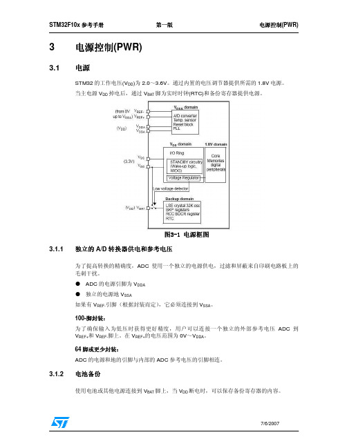
STM32F10x参考手册第一版STM32F10x参考手册1文档中的约定 (1)1.1寄存器描述中使用的缩写列表 (1)2存储器和总线构架 (2)2.1系统构架 (2)2.2存储器组织 (3)2.3存储器映像 (4)2.3.1外设存储器映像 (5)2.3.2嵌入式SRAM (6)2.3.3位段 (6)2.3.4嵌入式闪存 (6)2.4启动配置 (8)3电源控制(PWR) (9)3.1电源 (9)3.1.1独立的A/D转换器供电和参考电压 (9)3.1.2电池备份 (9)3.1.3电压调节器 (10)3.2电源管理器 (10)3.2.1上电复位(POR)和掉电复位(PDR) (10)3.2.2可编程电压监测器(PVD) (10)3.3低功耗模式 (11)3.3.1降低系统时钟 (12)3.3.2外部时钟的控制 (12)3.3.3睡眠模式 (12)3.3.4停止模式 (13)3.3.5待机模式 (14)3.3.6低功耗模式下的自动唤醒(AWU) (15)3.4电源控制寄存器 (16)3.4.1电源控制寄存器(PWR_CR) (16)3.4.2电源控制/状态寄存器 (17)3.5PWR寄存器映像 (18)4复位和时钟控制 (19)4.1复位 (19)4.1.1系统复位 (19)4.1.2电源复位 (19)4.2时钟 (20)4.2.1HSE时钟 (22)4.2.2HSI时钟 (22)4.2.3PLL (23)4.2.4LSE时钟 (23)4.2.5LSI时钟 (23)4.2.6系统时钟(SYSCLK)选择 (24)4.2.7时钟安全系统(CSS) (24)4.2.8RTC时钟 (24)4.2.9看门狗时钟 (24)4.2.10时钟输出 (25)4.3RCC寄存器描述 (26)4.3.1时钟控制寄存器(RCC_CR) (26)4.3.2时钟配置寄存器(RCC_CFGR) (27)4.3.3时钟中断寄存器 (RCC_CIR) (29)4.3.4APB2外设复位寄存器 (RCC_APB2RSTR) (32)4.3.5APB1外设复位寄存器 (RCC_APB1RSTR) (33)4.3.6AHB外设时钟使能寄存器 (RCC_AHBENR) (35)4.3.7APB2外设时钟使能寄存器(RCC_APB2ENR) (36)4.3.8APB1外设时钟使能寄存器(RCC_APB1ENR) (37)4.3.9备份域控制寄存器 (RCC_BDCR) (39)4.3.10控制/状态寄存器 (RCC_CSR) (40)4.4RCC寄存器映像 (43)5通用和复用功能I/O(GPIO和AFIO) (44)5.1GPIO功能描述 (44)5.1.1通用I/O(GPIO) (45)5.1.2单独的位设置或位清除 (45)5.1.3外部中断/唤醒线 (46)5.1.4复用功能(AF) (46)5.1.5软件重新映射I/O复用功能 (46)5.1.6GPIO锁定机制 (46)5.1.7输入配置 (46)5.1.8输出配置 (47)5.1.9复用功能配置 (48)5.2GPIO寄存器描述 (50)5.2.1端口配置低寄存器(GPIOx_CRL) (x=A..E) (50)5.2.2端口配置高寄存器(GPIOx_CRH) (x=A..E) (51)5.2.3端口输入数据寄存器(GPIOx_IDR) (x=A..E) (52)5.2.4端口输出数据寄存器(GPIOx_ODR) (x=A..E) (52)5.2.5端口位设置/复位寄存器(GPIOx_BSRR) (x=A..E) (53)5.2.6端口位复位寄存器(GPIOx_BRR) (x=A..E) (53)5.2.7端口配置锁定寄存器(GPIOx_LCKR) (x=A..E) (54)5.3复用功能I/O和调试配置(AFIO) (55)5.3.1把OSC_IN/OSC_OUT引脚作为GPIO端口PD0/PD1 (55)5.3.2BXCAN复用功能重映射 (55)5.3.3JTAG/SWD复用功能重映射 (55)5.3.4定时器复用功能重映射 (56)5.3.5USART复用功能重映射 (57)5.3.6I2C 1 复用功能重映射 (58)5.3.7SPI 1复用功能重映射 (58)5.4AFIO寄存器描述 (59)5.4.1复用重映射和调试I/O配置寄存器(AFIO_MAPR) (60)5.4.2外部中断配置寄存器1(AFIO_EXTICR1) (62)5.4.3外部中断配置寄存器2(AFIO_EXTICR2) (62)5.4.4外部中断配置寄存器3(AFIO_EXTICR3) (63)5.4.5外部中断配置寄存器4(AFIO_EXTICR4) (63)5.5GPIO 和AFIO寄存器地址映象 (64)5.5.1GPIO寄存器地址映象 (64)5.5.2AFIO寄存器地址映象 (65)6中断和事件 (66)6.1嵌套向量中断控制器(NVIC) (66)6.1.1系统嘀嗒(SysTick)校准值寄存器 (66)6.1.2中断和异常向量 (66)6.2外部中断/事件控制器(EXTI) (68)6.2.1主要特性 (68)6.2.2框图 (69)6.2.3唤醒事件管理 (69)6.2.4功能说明 (69)6.2.5外部中断/事件线路映像 (71)6.3EXTI 寄存器描述 (72)6.3.1外部中断/事件寄存器映像 (75)7DMA 控制器(DMA) (76)7.1简介 (76)7.2主要特性 (76)7.3功能描述 (77)7.3.1DMA处理 (77)7.3.2仲裁器 (77)7.3.3DMA 通道 (78)7.3.4错误管理 (79)7.3.5DMA请求映像 (79)7.4DMA寄存器 (82)7.4.1DMA中断状态寄存器(DMA_ISR) (82)7.4.2DMA中断标志清除寄存器(DMA_IFCR) (82)7.4.3DMA通道x配置寄存器(DMA_CCRx)(x = 1...7).. (83)7.4.4DMA通道x传输数量寄存器(DMA_CNDTRx)(x = 1...7) (85)7.4.5DMA通道x外设地址寄存器(DMA_CPARx)(x = 1...7).. (85)7.4.6DMA通道x存储器地址寄存器(DMA_CPARx)(x = 1...7).. (85)7.5DMA寄存器映像 (86)8实时时钟(RTC) (88)8.1简介 (88)8.2主要特性 (88)8.3功能描述 (88)8.3.1概述 (88)8.3.2复位过程 (90)8.3.3读RTC寄存器 (90)8.3.4配置RTC寄存器 (90)8.3.5RTC标志的设置 (90)8.4RTC寄存器描述 (91)8.4.1RTC控制寄存器高位(RTC_CRH) (91)8.4.2RTC控制寄存器低位(RTC_CRL) (92)8.4.3RTC预分频装载寄存器(RTC_PRLH/RTC_PRLL) (93)8.4.4RTC预分频分频因子寄存器(RTC_DIVH / RTC_DIVL) (94)8.4.5RTC计数器寄存器 (RTC_CNTH / RTC_CNTL) (95)8.4.6RTC闹钟寄存器(RTC_ALRH/RTC_ALRL) (95)8.5RTC寄存器映像 (97)9备份寄存器(BKP) (98)9.1简介 (98)9.2特性 (98)9.3侵入检测 (98)9.4RTC校准 (98)9.5BKP寄存器描述 (99)9.5.1备份数据寄存器x(BKP_DRx) (x = 1 ... 10) (99)9.5.2RTC时钟校准寄存器(BKP_RTCCR) (99)9.5.3备份控制寄存器(BKP_CR) (99)9.5.4备份控制/状态寄存器(BKP_CSR) (100)9.6BKP寄存器映像 (101)10独立看门狗(IWDG) (103)10.1简介 (103)10.1.1硬件看门狗 (103)10.1.2寄存器访问保护 (103)10.1.3调试模式 (104)10.2IWDG寄存器描述 (104)10.2.1键寄存器(IWDG_KR) (104)10.2.2预分频寄存器(IWDG_PR) (105)10.2.3重装载寄存器(IWDG_RLR) (106)10.2.4状态寄存器(IWDG_SR) (106)10.3IWDG寄存器映像 (107)11窗口看门狗(WWDG) (108)11.1简介 (108)11.2主要特性 (108)11.3功能描述 (108)11.4如何编写看门狗超时程序 (109)11.5调试模式 (110)11.6寄存器描述 (111)11.6.1控制寄存器(WWDG_CR) (111)11.6.2配置寄存器(WWDG_CFR) (111)11.6.3状态寄存器(WWDG_SR) (112)11.7WWDG寄存器映像 (113)12高级控制定时器(TIM1) (114)12.1简介 (114)12.2主要特性 (114)12.3框图 (115)12.4功能描述 (116)12.4.1时基单元 (116)12.4.2计数器模式 (117)12.4.3重复向下计数器 (125)12.4.4时钟选择 (126)12.4.5捕获/比较通道 (129)12.4.6输入捕获模式 (131)12.4.7PWM输入模式 (132)12.4.8强置输出模式 (132)12.4.9输出比较模式 (133)12.4.10PWM 模式 (134)12.4.11互补输出和死区插入 (136)12.4.12使用刹车功能 (138)12.4.13在外部事件时清除OCxREF信号 (139)12.4.14六步PWM的产生 (140)12.4.15单脉冲模式 (141)12.4.16编码器接口模式 (143)12.4.17定时器输入异或功能 (144)12.4.18与霍尔元件的接口 (145)12.4.19定时器和外部触发的同步 (146)12.4.20定时器同步 (149)12.4.21调试模式 (149)12.5TIM1寄存器描述 (150)12.5.1控制寄存器1(TIM1_CR1) (150)12.5.2控制寄存器2(TIM1_CR2) (151)12.5.3从模式控制寄存器(TIM1_SMCR) (153)12.5.4DMA/中断使能寄存器(TIM1_DIER) (154)12.5.5状态寄存器(TIM1_SR) (156)12.5.6事件产生寄存器(TIM1_EGR) (157)12.5.7捕获/比较模式寄存器1(TIM1_CCMR1) (158)12.5.8捕获/比较模式寄存器2(TIM1_CCMR2) (161)12.5.10计数器(TIM1_CNT) (165)12.5.11预分频器(TIM1_PSC) (165)12.5.12自动重装载寄存器(TIM1_ARR) (165)12.5.13周期计数寄存器(TIM1_RCR) (166)12.5.14捕获/比较寄存器1(TIM1_CCR1) (166)12.5.15捕获/比较寄存器2(TIM1_CCR2) (167)12.5.16捕获/比较寄存器3(TIM1_CCR3) (167)12.5.17捕获/比较寄存器(TIM1_CCR4) (168)12.5.18刹车和死区寄存器(TIM1_BDTR) (168)12.5.19DMA控制寄存器(TIM1_DCR) (170)12.5.20连续模式的DMA地址(TIM1_DMAR) (170)12.6TIM1寄存器图 (171)13通用定时器(TIMx) (173)13.1概述 (173)13.2主要特性 (173)13.3框图 (174)13.4功能描述 (175)13.4.1时基单元 (175)13.4.2计数器模式 (176)13.4.3时钟选择 (183)13.4.4捕获/比较通道 (185)13.4.5输入捕获模式 (187)13.4.6PWM输入模式 (187)13.4.7强置输出模式 (188)13.4.8输出比较模式 (188)13.4.9PWM 模式 (189)13.4.10单脉冲模式 (191)13.4.11在外部事件时清除OCxREF信号 (193)13.4.12编码器接口模式 (193)13.4.13定时器输入异或功能 (195)13.4.14定时器和外部触发的同步 (195)13.4.15定时器同步 (198)13.4.16调试模式 (202)13.5TIMx寄存器描述 (203)13.5.2控制寄存器2(TIMx_CR2) (205)13.5.3从模式控制寄存器(TIMx_SMCR) (206)13.5.4DMA/中断使能寄存器(TIMx_DIER) (207)13.5.5状态寄存器(TIMx_SR) (209)13.5.6事件产生寄存器(TIMx_EGR) (211)13.5.7捕获/比较模式寄存器1(TIMx_CCMR1) (212)13.5.8捕获/比较模式寄存器2(TIMx_CCMR2) (215)13.5.9捕获/比较使能寄存器(TIMx_CCER) (216)13.5.10计数器(TIMx_CNT) (218)13.5.11预分频器(TIMx_PSC) (218)13.5.12自动重装载寄存器(TIMx_ARR) (218)13.5.13捕获/比较寄存器1(TIMx_CCR1) (219)13.5.14捕获/比较寄存器2(TIMx_CCR2) (220)13.5.15捕获/比较寄存器3(TIMx_CCR3) (220)13.5.16捕获/比较寄存器(TIMx_CCR4) (221)13.5.17DMA控制寄存器(TIMx_DCR) (221)13.5.18连续模式的DMA地址(TIMx_DMAR) (222)13.6TIMx寄存器图 (223)14控制器局域网(bxCAN) (225)14.1简介 (225)14.2主要特点 (225)14.3总体描述 (225)14.3.1CAN 2.0B内核 (226)14.3.2控制、状态和配置寄存器 (226)14.3.3发送邮箱 (226)14.3.4接收过滤器 (226)14.3.5接收FIFO (227)14.4工作模式 (228)14.4.1初始化模式 (228)14.4.2正常模式 (228)14.4.3睡眠模式(低功耗) (228)14.4.4测试模式 (229)14.4.5静默模式 (229)14.4.6环回模式 (229)14.4.7环回静默模式 (230)14.5功能描述 (230)14.5.1发送处理 (230)14.5.2时间触发通信模式 (232)14.5.3接收管理 (232)14.5.4标识符过滤 (234)14.5.5报文存储 (238)14.5.6出错管理 (239)14.5.7位时间特性 (239)14.6中断 (241)14.7寄存器访问保护 (243)14.8CAN 寄存器描述 (243)14.8.1控制和状态寄存器 (243)14.8.2邮箱寄存器 (255)14.8.3CAN过滤器寄存器 (260)14.9bxCAN寄存器列表 (264)15I2C接口 (267)15.1介绍 (267)15.2主要特点 (267)15.3概述 (268)15.4功能描述 (269)15.4.1I2C从模式 (269)15.4.2I2C主模式 (271)15.4.3错误条件 (274)15.4.4SDA/SCL线控制 (275)15.4.5SMBus (275)15.4.6DMA请求 (277)15.4.7包错误校验(PEC) (278)15.5中断请求 (279)15.6I2C寄存器描述 (281)15.6.1控制寄存器1(I2C_CR1) (281)15.6.2控制寄存器2(I2C_CR2) (283)15.6.3自身地址寄存器1 (I2C_OAR1) (284)15.6.4自身地址寄存器2(I2C_OAR2) (285)15.6.5数据寄存器(I2C_DR) (285)15.6.6状态寄存器1(I2C_SR1) (285)15.6.7状态寄存器2 (I2C_SR2) (288)15.6.8时钟控制寄存器(I2C_CCR) (289)15.6.9TRISE寄存器(I2C_TRISE) (290)15.7I2C寄存器地址映象 (291)16串行外设接口(SPI) (292)16.1简介 (292)16.2主要特征 (292)16.3功能描述 (292)16.3.1概述 (292)16.3.2SPI从模式 (295)16.3.3SPI主模式 (296)16.3.4单向通信 (297)16.3.5状态标志 (297)16.3.6CRC计算 (298)16.3.7利用DMA的SPI通信 (299)16.3.8错误标志 (299)16.3.9中断 (300)16.4SPI寄存器描述 (300)16.4.1SPI控制寄存器1(SPI_CR1) (300)16.4.2SPI控制寄存器2(SPI_CR2) (302)16.4.3SPI 状态寄存器(SPI_SR) (303)16.4.4SPI 数据寄存器(SPI_DR) (304)16.4.5SPI CRC多项式寄存器(SPI_CRCPR) (304)16.4.6SPI Rx CRC寄存器(SPI_RXCRCR) (305)16.4.7SPI Tx CRC寄存器(SPI_TXCRCR) (305)16.5SPI 寄存器地址映象 (306)17USART收发器(USART) (307)17.1介绍 (307)17.2概述 (308)17.2.1框图 (309)17.2.2USART 特征描述 (310)17.2.3发送器 (310)17.2.4接收器 (312)17.2.5分数波特率的产生 (315)17.2.617.2.6 多处理器通信 (316)17.2.7校验控制 (317)17.2.8LIN(局域互联网)模式 (318)17.2.9USART 同步模式 (320)17.2.10单线半双工通信 (322)17.2.11智能卡 (322)17.2.12IrDA SIR ENDEC 功能块 (324)17.2.13利用DMA连续通信 (325)17.2.14硬件流控制 (326)17.3中断请求 (327)17.4USART寄存器描述 (329)17.4.1状态寄存器(USART_SR) (329)17.4.2数据寄存器(USART_DR) (330)17.4.3波特比率寄存器(USART_BRR) (331)17.4.4控制寄存器1 (USART_CR1) (331)17.4.5控制寄存器2(USART_CR2) (333)17.4.6控制寄存器3(USART_CR3) (335)17.4.7保护时间和预分频寄存器(USART_GTPR) (336)17.5USART寄存器地址映象 (338)18USB全速设备接口(USB) (339)18.1导言 (339)18.2主要特征 (339)18.3方框图 (339)18.4功能描述 (340)18.4.1USB功能模块描述 (341)18.5编程中需要考虑的问题 (342)18.5.1通用USB设备编程 (342)18.5.2系统复位和上电复位 (342)18.5.3双缓冲端点 (346)18.5.4同步传输 (347)18.5.5挂起/恢复事件 (348)18.6USB寄存器描述 (350)18.6.1通用寄存器 (350)18.6.2端点寄存器 (355)18.6.3缓冲区描述表 (358)18.7USB寄存器映像 (361)19模拟/数字转换(ADC) (363)19.1介绍 (363)19.2主要特征 (363)19.3引脚描述 (365)19.4功能描述 (365)19.4.1ADC开关控制 (365)19.4.2ADC时钟 (365)19.4.3通道选择 (365)19.4.4单次转换模式 (366)19.4.5连续转换模式 (366)19.4.6时序图 (367)19.4.7模拟看门狗 (368)19.4.8扫描模式 (368)19.4.9注入通道管理 (369)19.4.10间断模式 (369)19.5校准 (370)19.6数据对齐 (371)19.7可编程的通道采样时间 (371)19.8外部触发转换 (371)19.9DMA请求 (372)19.10双ADC模式 (372)19.10.1同时注入模式 (374)19.10.2同时规则模式 (374)19.10.3快速交替模式 (375)19.10.4慢速交替模式 (375)19.10.5交替触发模式 (376)19.10.6独立模式 (377)19.10.7混合的规则/注入同步模式 (377)19.10.8混合的同步规则+交替触发模式 (377)19.10.9混合同步注入+交替模式 (378)19.11温度传感器 (378)19.12中断 (379)19.13ADC寄存器描述 (381)19.13.1ADC状态寄存器(ADC_SR) (381)19.13.2ADC控制寄存器1(ADC_CR1) (382)19.13.3ADC控制寄存器2(ADC_CR2) (384)19.13.4ADC采样时间寄存器1(ADC_SMPR1) (387)19.13.5ADC采样时间寄存器2(ADC_SMPR2) (387)19.13.6ADC注入通道数据偏移寄存器x (ADC_JOFRx)(x=1..4) (388)19.13.7ADC看门狗高阀值寄存器(ADC_HTR) (388)19.13.8ADC看门狗低阀值寄存器(ADC_LRT) (388)19.13.9ADC规则序列寄存器1(ADC_SQR1) (390)19.13.10ADC规则序列寄存器2(ADC_SQR2) (390)19.13.11ADC规则序列寄存器3(ADC_SQR3) (391)19.13.12ADC注入序列寄存器(ADC_JSQR) (391)19.13.13ADC 注入数据寄存器x (ADC_JDRx) (x= 1..4) (392)19.13.14ADC规则数据寄存器(ADC_DR) (392)19.14ADC寄存器地址映像 (394)20调试支持(DBG) (396)20.1概况 (396)20.2ARM参考文献 (397)20.3SWJ调试端口(serial wire and JTAG) (397)20.3.1JTAG-DP和SW-DP切换的机制 (397)20.4引脚分布和调试端口脚 (398)20.4.1SWJ调试端口脚 (398)20.4.2灵活的SWJ-DP脚分配 (398)20.4.3JTAG脚上的内部上拉和下拉 (399)20.4.4利用串行接口并释放不用的调试脚作为普通I/O口 (400)20.5STM32F10x JTAG TAP 连接 (400)20.6ID 代码和锁定机制 (401)20.6.1MCU DEVICE ID编码 (401)20.6.2TMC TAP (401)20.6.3Cortex-M3 TAP (401)20.6.4Cortex-M3 JEDEC-106 ID代码 (401)20.7JTAG调试端口 (402)20.8SW调试端口 (403)20.8.1SW协议介绍 (403)20.8.2SW协议序列 (403)20.8.3SW-DP状态机(Reset, idle states, ID code) (404)20.8.4DP和AP读/写访问 (404)20.8.5SW-DP寄存器 (405)20.8.6SW-AP寄存器 (405)20.9对于JTAG-DP或SWDP都有效的AHB-AP (AHB 访问端口) (405)20.10内核调试 (406)20.11调试器主机在系统复位下的连接能力 (407)20.12FPB (Flash patch breakpoint) (407)20.13DWT(data watchpoint trigger) (407)20.14ITM (instrumentation trace macrocell) (408)20.14.1概述 (408)20.14.2时间戳包,同步和溢出包 (408)20.15MCU调试模块(MCUDBG) (409)20.15.1低功耗模式的调试支持 (409)20.15.2支持定时器和看门狗和bxCAN的调试 (409)20.15.3调试MCU配置寄存器 (410)20.16TPIU (trace port interface unit) (411)20.16.1导言 (411)20.16.2跟踪引脚分配 (412)20.16.3TPUI格式器 (414)20.16.4TPUI帧异步包 (414)20.16.5同步帧包的发送 (415)20.16.6同步模式 (415)20.16.7异步模式 (415)20.16.8TRACECLKIN在STM32F10x内部的连接 (415)20.16.9TPIU寄存器 (416)20.16.10配置的例子 (416)20.17DBG寄存器地址映象 (417)STM32F10x参考手册第一版文档中的约定1 文档中的约定1.1 寄存器描述中使用的缩写列表在对寄存器的描述中使用了下列缩写:read / write (rw) 软件能读写此位。

数据手册STM32F103x8 STM32F103xB中等容量增强型,32位基于ARM 核心的带64或128K 字节闪存的微控制器USB 、CAN 、7个定时器、2个ADC 、9个通信接口功能■ 内核:ARM 32位的Cortex™-M3 CPU− 最高72MHz 工作频率,在存储器的0等待周期访问时可达1.25DMips/MHz(Dhrystone 2.1)− 单周期乘法和硬件除法■ 存储器− 从64K 或128K 字节的闪存程序存储器 − 高达20K 字节的SRAM ■ 时钟、复位和电源管理− 2.0~3.6伏供电和I/O 引脚 − 上电/断电复位(POR/PDR)、可编程电压监测器(PVD)− 4~16MHz 晶体振荡器− 内嵌经出厂调校的8MHz 的RC 振荡器 − 内嵌带校准的40kHz 的RC 振荡器 − 产生CPU 时钟的PLL− 带校准功能的32kHz RTC 振荡器 ■ 低功耗− 睡眠、停机和待机模式− V BAT 为RTC 和后备寄存器供电■ 2个12位模数转换器,1μs 转换时间(多达16个输入通道)− 转换范围:0至3.6V − 双采样和保持功能 − 温度传感器 ■ DMA :− 7通道DMA 控制器− 支持的外设:定时器、ADC 、SPI 、I 2C 和USART ■ 多达80个快速I/O 端口− 26/37/51/80个I/O 口,所有I/O 口可以映像到16个外部中断;几乎所有端口均可容忍5V 信■ 调试模式− 串行单线调试(SWD)和JTAG 接口■ 多达7个定时器− 3个16位定时器,每个定时器有多达4个用于输入捕获/输出比较/PWM 或脉冲计数的通道和增量编码器输入− 1个16位带死区控制和紧急刹车,用于电机控制的PWM 高级控制定时器− 2个看门狗定时器(独立的和窗口型的) − 系统时间定时器:24位自减型计数器 ■ 多达9个通信接口− 多达2个I 2C 接口(支持SMBus/PMBus) − 多达3个USART 接口(支持ISO7816接口,LIN ,IrDA 接口和调制解调控制) − 多达2个SPI 接口(18M 位/秒) − CAN 接口(2.0B 主动) − USB 2.0全速接口 ■ CRC 计算单元,96位的芯片唯一代码 ■ ECOPACK ®封装 表1 器件列表本文档英文原文下载地址: /stonline/products/literature/ds/13587.pdf本页已使用福昕阅读器进行编辑。


STM32启动模式说明 渤海三叠浪 理论部分理论部分Boot mode selection pins Boot mode AliasingBOOT1 BOOT0X 0 User Flash memory X 0 User Flash memory User Flash memory is selected as the boot space User Flash memory is selected as the boot space 0 1 System memory 0 1 System memory System memory is selected as the boot space System memory is selected as the boot space1 1 Embedded SRAM 1 1 Embedded SRAM Embedded SRAM is selected as Embedded SRAM is selected as Embedded SRAM is selected as the boot space the boot space the boot space《STM32三种启动模式中存储器的存储介质三种启动模式中存储器的存储介质》》引自STM32的博客STM32三种启动模式对应的存储介质均是芯片内置的三种启动模式对应的存储介质均是芯片内置的,,它们是它们是::1)用户闪存用户闪存 = = = 芯片内置的芯片内置的Flash Flash。
2)SRAM = SRAM = 芯片内置的芯片内置的RAM 区,就是内存啦就是内存啦。
3)系统存储器系统存储器 = = = 芯片内部一块特定的区域芯片内部一块特定的区域芯片内部一块特定的区域,,芯片出厂时在这个区域预置了一段Bootloader Bootloader,,就是通常说的ISP 程序程序。
这个区域的内容在芯片出厂后没有人能够在芯片出厂后没有人能够修改或擦除修改或擦除修改或擦除,,即它是一个ROM 区。

STM32主机使用说明书一、介绍纳英特STM32智能机器人平台采用ST公司的STM32103FVET6作为主控制器,内核采用了ARM公司Cortex M3存储容量大、运行速度快、外围接口丰富、稳定可靠,支持图形化及C语言编程,同时兼容原配件,是您进行竞赛、教学的理想选择。
二、布局(根据盒子图片再做)三、操作3.1搭建根据需要搭建机器人整机,连接传感器与马达,连接马达等,具体搭建方法请参考相应的项目手册,如灭火、足球项目的不同方案。
3.2编程根据项目需要对机器人进行编程。
可使用图形化的积木式编程模式,也可以使用C语言模式,软件的使用方法请参阅《纳英特积木式编程系统使用说明书》。
3.3下载软件上编程完成,编译通过,要下载时先把数据线连接好,再开启电源,这时主机会自动进入下载模式,被电脑识别为一个U盘,然后在软件上点击下载即可。
注:下载过程其实是将软件编译好的可执行文件***.bin文件拷贝到主机的这个U盘中,可执行的文件名是8.3格式的短文件名,不支持中文。
当软件新建的项目名为中文名时,下载时软件会跳出一个另存为的对话框,以英文或数字命名存储到U 盘即可;当项目名为英文或数字时,生成的***.bin文件的文件名即为项目名。
3.4运行程序下载完后,会保存在主机的U盘中,可同时存多个程序。
运行时,选择所需要的运行的程序名称即可。
主机开机后,屏幕上显示4个菜单选项,可通过上下键选择。
第一项为“运行”,后面显示的是当前的程序文件名,如果要运行的程序就是当前显示的程序,直接按确认键即可;如果要运行的程序不是当前显示的程序,则进入“选择程序”一项,屏幕会显示U盘中所存在的每一个程序名,通过上下键选择要运行的程序按确认键返回到原来的界面,再选择“运行”,按确认键。
3.5调试观察机器人运行结果是否符合预期的要求,如不符合,可重复以上4个步骤反复调试,直到符合预期的要求。
四、测试和设置主机固件中包含一个硬件的测试和设置的程序,在开机后的界面中选择“测试设置”,按确认键进入,屏幕显示“测试程序”,“参数修改”,“蓝牙设置”,“系统信息”。

23 串行外设接口(SPI)小容量产品是指闪存存储器容量在16K 至32K 字节之间的STM32F101xx、STM32F102xx和STM32F103xx微控制器。
中容量产品是指闪存存储器容量在64K至128K字节之间的STM32F101xx、STM32F102xx和STM32F103xx微控制器。
大容量产品是指闪存存储器容量在256K至512K字节之间的STM32F101xx和STM32F103xx微控制器。
互联型产品是指STM32F105xx和STM32F107xx微控制器。
除非特别说明,本章描述的模块适用于整个STM32F10xxx微控制器系列。
23.1 SPI简介在大容量产品和互联型产品上,SPI接口可以配置为支持SPI协议或者支持I2S音频协议。
SPI接口默认工作在SPI方式,可以通过软件把功能从SPI模式切换到I2S模式。
在小容量和中容量产品上,不支持I2S音频协议。
串行外设接口(SPI)允许芯片与外部设备以半/全双工、同步、串行方式通信。
此接口可以被配置成主模式,并为外部从设备提供通信时钟(SCK)。
接口还能以多主配置方式工作。
它可用于多种用途,包括使用一条双向数据线的双线单工同步传输,还可使用CRC校验的可靠通信。
I2S也是一种3引脚的同步串行接口通讯协议。
它支持四种音频标准,包括飞利浦I2S标准,MSB 和LSB对齐标准,以及PCM标准。
它在半双工通讯中,可以工作在主和从2种模式下。
当它作为主设备时,通过接口向外部的从设备提供时钟信号。
警告:由于 SPI3/I2S3 的部分引脚与 JTAG 引脚共享 (SPI3_NSS/I2S3_WS 与 JTDI ,SPI3_SCK/I2S3_CK与JTDO),因此这些引脚不受IO控制器控制,他们(在每次复位后)被默认保留为JTAG用途。
如果用户想把引脚配置给SPI3/I2S3,必须(在调试时)关闭JTAG并切换至SWD接口,或者(在标准应用时)同时关闭JTAG和SWD接口。

December 2007 Rev 11/28UM0486User manualSTM3210B-MCKIT motor control starter kitIntroductionThe STM3210B-MCKIT starter kit is an integrated system designed to provide a complete, ready-to-use motor control application developed around the STMicroelectronics STM32 microcontroller. This starter kit is particularly suited to drive 3-phase brushless motors (either AC induction or permanent magnet types) and demonstrates how effectively the STM32 microcontrollers can be used in real-world motor control applications.Drive is based on sensored field oriented control (FOC) for three-phase motors using the shunt resistor current measurement method for closed loop torque control. Position measurement is implemented using Encoder sensor or T achometer. The inverter is driven using the space vector PWM modulation technique.Y ou can run the STM3210B-MCKIT starter kit in several ways:●As a plug-and play demo, out of the box, with the provided PMSM motor, in open or closed loop.●With an AC induction motor in standalone mode, after programming the microcontroller.However, the main advantage of the STM3210B-MCKIT is that you can use it to create your own applications and re-program the STM32 microcontroller. Y ou can develop your own applications using the dedicated software libraries provided in the starter kit in conjunction with the EWARM KickStart Edition development environment from IAR. In addition, the PMSM and AC induction motor applications delivered with the starter kit are intended to provide a sound basis for your own application developments. Do not hesitate to fine tune them to fit your specific requirements.In this manual, you will find information on:●The STM3210B-MCKIT starter kit components, and how to set up the hardware to run the provided PMSM motor or an AC induction motor ●How to run the STM3210B-MCKIT starter kit in standalone mode ●How to re-program the STM32 microcontroller to run your own applicationFor information on the features of the STM32 microcontroller, refer to the datasheet. The STM32 evaluation board features, peripherals, and connectors are described in the STM3210B-EVAL User Manual (UM0426).For information on the PMSM and AC induction motor software libraries and how to use them in motor control application development projects, refer to the PMSM Field Oriented Control Software Library User Manual (UM0492) and the AC Induction Motor IFOC Software Library User Manual (UM0483) respectively. Y ou will find these manuals, and all related documentation on the STM3210B-MCKIT CD-ROM.Contents UM0486Contents1STM32-MCKIT hardware setup . . . . . . . . . . . . . . . . . . . . . . . . . . . . . . . . . 51.1Package checklist . . . . . . . . . . . . . . . . . . . . . . . . . . . . . . . . . . . . . . . . . . . . 51.1.1Hardware . . . . . . . . . . . . . . . . . . . . . . . . . . . . . . . . . . . . . . . . . . . . . . . . . 51.1.2Firmware . . . . . . . . . . . . . . . . . . . . . . . . . . . . . . . . . . . . . . . . . . . . . . . . . 61.1.3Software . . . . . . . . . . . . . . . . . . . . . . . . . . . . . . . . . . . . . . . . . . . . . . . . . . 61.1.4Documentation . . . . . . . . . . . . . . . . . . . . . . . . . . . . . . . . . . . . . . . . . . . . . 71.1.5Components not provided . . . . . . . . . . . . . . . . . . . . . . . . . . . . . . . . . . . . 71.1.6Permanent magnet synchronous motor (PMSM) . . . . . . . . . . . . . . . . . . . 71.1.7AC induction motor . . . . . . . . . . . . . . . . . . . . . . . . . . . . . . . . . . . . . . . . . 81.2Hardware configuration for PMSM motor (default) . . . . . . . . . . . . . . . . . . . 91.3Hardware configuration for AC induction motor . . . . . . . . . . . . . . . . . . . . 111.4Power supply connections . . . . . . . . . . . . . . . . . . . . . . . . . . . . . . . . . . . . 132Running the starter kit . . . . . . . . . . . . . . . . . . . . . . . . . . . . . . . . . . . . . . 142.1Running the PMSM motor . . . . . . . . . . . . . . . . . . . . . . . . . . . . . . . . . . . . 152.1.1LCD display in speed control mode . . . . . . . . . . . . . . . . . . . . . . . . . . . . 162.1.2LCD display in torque control mode . . . . . . . . . . . . . . . . . . . . . . . . . . . . 192.1.3PMSM motor fault messages . . . . . . . . . . . . . . . . . . . . . . . . . . . . . . . . . 192.1.4Running your own PMSM motor . . . . . . . . . . . . . . . . . . . . . . . . . . . . . . 202.2Running an AC induction motor . . . . . . . . . . . . . . . . . . . . . . . . . . . . . . . . 212.2.1LCD display in speed control mode . . . . . . . . . . . . . . . . . . . . . . . . . . . . 212.2.2LCD display in torque control mode . . . . . . . . . . . . . . . . . . . . . . . . . . . . 222.2.3AC motor control variables that can be monitored . . . . . . . . . . . . . . . . . 232.2.4AC induction motor fault messages . . . . . . . . . . . . . . . . . . . . . . . . . . . . 232.2.5Running your own AC motor . . . . . . . . . . . . . . . . . . . . . . . . . . . . . . . . . 243Creating your custom application . . . . . . . . . . . . . . . . . . . . . . . . . . . . . 253.1Installing the IAR EWARM KickStart Edition (32KB limitation) . . . . . . . . . 253.2Developing your own application . . . . . . . . . . . . . . . . . . . . . . . . . . . . . . . 25Appendix A Additional information. . . . . . . . . . . . . . . . . . . . . . . . . . . . . . . . . . . . 26A.1Recommended reading. . . . . . . . . . . . . . . . . . . . . . . . . . . . . . . . . . . . . . . 26A.2Software upgrades . . . . . . . . . . . . . . . . . . . . . . . . . . . . . . . . . . . . . . . . . . 26 2/28UM0486ContentsA.3Getting technical support . . . . . . . . . . . . . . . . . . . . . . . . . . . . . . . . . . . . . 26 Revision history . . . . . . . . . . . . . . . . . . . . . . . . . . . . . . . . . . . . . . . . . . . . . . . . . . . . 273/28UM04864/28Safety warningsGeneralIn operation, the STM32-MCKIT starter kit has uninsulated wires, moving or rotating parts (when connected to a motor), as well as hot surfaces. In case of improper use, incorrect installation or misuse, there is danger of serious personal injury and damage to property. All operations, installation and maintenance are to be carried out by skilled technical personnel (applicable accident prevention rules must be observed).When the motor control board is supplied with voltages greater than 30 V AC/DC, all of the board and components must be considered “hot”, and any contact with the board must be avoided. The operator should stay away from the board as well (risk of projection of material in case of components destruction, especially when powering the board with high voltages). The rotating parts of motors are also a source of danger.The STM32-MCKIT starter kit contains electrostatic sensitive components which may be damaged through improper use.Intended useThe STM32-MCKIT starter kit is made of components designed for demonstration purposes and must not be included in electrical installations or machinery. Instructions about the setup and use of the STM32-MCKIT starter kit must be strictly observed.OperationAfter disconnecting the board from the voltage supply, several parts and power terminals must not be touched immediately because of possible energized capacitors or hot surfaces. Important notice to usersWhile every effort has been made to ensure the accuracy of all information in this document, STMicroelectronics assumes no liability to any party for any loss or damage caused by errors or omissions or by statements of any kind in this document, its updates, supplements, or special editions, whether such errors are omissions or statements resulting from negligence, accident, or any other cause.5/281 STM32-MCKIT hardware setupThis section provides a detailed description of the components included in the STM32-MCKIT starter kit. It also describes the default settings for a permanent magnet sensoredmotor (PMSM), and explains how to change them to use an AC induction motor.1.1 Package checklistFigure 1 shows the layout and connections of the major components of the STM32-MCKITstarter kit.Figure 1.STM32-MCKIT layout1.1.1 HardwareThe STM32-MCKIT starter kit includes the following items:●The MB459B motor control evaluation board (1)This board is described in the MB459B Motor Control Board User Manual (UM0379)provided on the STM32-MCKIT CD-ROM.●The MB525 STM32 evaluation board (2)This board is described in the STM3210B-EVAL User Manual (UM0426) provided onthe STM32-MCKIT CD-ROM.SHINANOMOTOR MOTOR CONTROLEVALUA TIONBOARDMB459BSTM32EVAL BOARD MB525JTAG ISOLA TIONBOARD MB535B TR30R AC/DCPower Adapter 6187JLINK USB-JT AGDEBUGGER931025Encoder4 Motor phases●An MB535B opto-isolation JT AG board (3)This board is described in the JTAG Opto-isolation Board User Manual (UM0378)provided on the STM32-MCKIT CD-ROM.The purpose of the JTAG opto-isolation board is to provide galvanic isolation betweenthe J-link debugger/programmer and the STM32 evaluation board. It helps to preventaccidental damage to the PC in the event of a catastrophic failure on the motor controlboard. This isolation barrier also solves the problem of the PC, JTAG debugger andmotor control board being at different ground potentials.● A J-link USB–JTAG debugger (4)The SEGGER J-link USB-JTAG debugger used in conjunction with the IAR EmbeddedWorkbench C/C++ 32 KB compiler allows you to re-program the Flash memory of theSTM32 microcontroller and to debug the software before using the application instandalone mode.● A 24V DC SHINANO PMSM motor (5)The motor included in the STM32-MCKIT starter kit is a SHINANO Inner rotor type 4-pole brushless DC motor with Hall sensor and encoder. For electrical specificationsand mechanical dimensions, refer to the SHINANO datasheets on the STM32-MCKITCD-ROM.●An auxiliary power supply block TR30R (6)●The following cables:–Motor cables (7)– A motor connector HE10 34-pin cable (8)– A USB cable (9)–Two JTAG cables (10)● A bag with three 0.1ohm resistors are included to configure the MB459B board fordriving an AC induction motor.●The STM32-MCKIT CD-ROM1.1.2 FirmwareThe STM32-MCKIT provides two firmware binary files:●The firmware for the PMSM motor●The firmware for the Selni AC induction motorWhen you receive the STM32-MCKIT, the STM32 microcontroller is programmed by defaultwith the PMSM standalone firmware.1.1.3 SoftwareThe STM32-MCKIT CD-ROM includes the following software:●The PMSM and AC induction motor software libraries6/281.1.4 DocumentationThe STM32-MCKIT CD-ROM also includes the following product documentation in PDFformat:●STM32-MCKIT Motor Control Kit User Manual (UM0486, the present manual)●PMSM Field Oriented Control Software Library User Manual (UM0492)●AC Induction Motor IFOC Software Library User Manual (UM0483)●STM3210B-EVAL User Manual (UM0426)●MB459B Motor Control Evaluation Board User Manual (UM0379)●JTAG Opto-isolation Board User Manual (UM0378)In the box with the STM32-MCKIT, you will also find:● A startup color poster which summarizes the main steps for running the motor controlkit●The MCD product finder●Product flyers and brochures●The MCD minirom● A guarantee record card1.1.5 ComponentsprovidednotThe STM32-MCKIT starter kit does not include:● A power supplyTo use the STM32-MCKIT starter kit with the provided PMSM motor, you need a 24V-3A minimum power supply. Y ou can order the SPU65-108 (24V - 3.3A - 80W) with S&TType connector (code P00) from SINPRO (/Sinpro).●An AC induction motorThe STM32-MCKIT can operate with an AC induction motor. The provided graphicaluser interface is designed to operate with the SELNI induction motor. It can be orderedas an accessory with the following order code: ST7MC-MOT/IND.To use the STM32-MCKIT starter kit with the Selni AC induction motor, you need a 42VDC or 32V eff AC power supply (polarity not important, GND recommended).1.1.6 Permanent magnet synchronous motor (PMSM)The PM synchronous motor is a rotating electric machine where the stator is a classic threephase stator like that of an induction motor and the rotor has surface-mounted permanentmagnets. In this respect, the PM synchronous motor is equivalent to an induction motorwhere the air gap magnetic field is produced by a permanent magnet. The use of apermanent magnet to generate a substantial air gap magnetic flux makes it possible todesign highly efficient PM motors.A PM synchronous motor is driven by sine wave voltage coupled with the given rotorposition. The generated stator flux together with the rotor flux, which is generated by a rotormagnet, defines the torque, and thus speed, of the motor. The sine wave voltage outputhave to be applied to the 3-phase winding system in a way that angle between the stator fluxand the rotor flux is kept close to 90° to get the maximum generated torque. T o meet thiscriterion, the motor requires electronic control for proper operation.7/28For a common 3-phase PM synchronous motor, a standard 3-phase power stage is used.The same power stage is used for AC induction and PMSM motors. The power stage utilizessix power transistors with independent switching. The power transistors are switched in thecomplementary mode. The sine wave output is generated using the space vector PWMtechnique.motor1.1.7 ACinductionThe AC induction motor is a rotating electric machine designed to operate from a three-phase source of alternating voltage. The stator is a classic three phase stator with thewinding displaced by 120°. The most common type of induction motor has a squirrel cagerotor in which aluminum conductors or bars are shorted together at both ends of the rotor bycast aluminum end rings. When three currents flow through the three symmetrically placedwindings, a sinusoidally distributed air gap flux generating the rotor current is produced. Theinteraction of the sinusoidally distributed air gap flux and induced rotor currents produces atorque on the rotor. The mechanical angular velocity of the rotor is lower then the angularvelocity of the flux wave by so called slip velocity.In adjustable speed applications, AC induction motors are powered by inverters. Theinverter converts DC power to AC power at the required frequency and amplitude. Theinverter consists of three half-bridge units where the upper and lower switches arecontrolled complementarily. As the power device's turn-off time is longer than its turn-ontime, some dead-time must be inserted between the turn-off of one transistor of the half-bridge and turn-on of its complementary device. The output voltage is mostly created by apulse width modulation (PWM) technique. The three-phase voltage waves are shifted 120°to each other and thus a three-phase motor can be supplied.8/281.2 Hardware configuration for PMSM motor (default)This section describes the procedure for operating the STM32-MCKIT with a PMSM motor.The default settings that are present on the STM32 evaluation board and on the motorcontrol evaluation board when you receive the STM32-MCKIT starter kit are intended for aPMSM motor.When you are running the PMSM motor, follow these steps:1.Verify that all the jumpers on the motor control board (MB459B) are in their defaultposition.Refer to Table1 for information on jumper settings, and if necessary, to the MB459BMotor Control Board User Manual for the location of the jumpers on the board.2. Verify that all of the STM32 evaluation board (MB525) jumpers are in their defaultposition.Refer to Table2 for information on jumper settings, and if necessary, to the STM3210B-EVAL board User Manual for the location of jumpers on the board.3. Verify that the PMSM motor cables are correctly plugged into the motor control board's"MOTOR" connectors (J5 and J8).The motor control board (MB459B), the STM32 evaluation board (MB525), the opto-isolation JTAG board (MB535B), and the provided PMSM motor are already assembledtogether over a metal support when you receive the kit.4. Verify that the STM32 evaluation board and the JT AG opto-isolation board (MB535B)are connected with the provided 20-pin JT AG cable.In this way, the STM32 evaluation board automatically supplies the opto-isolationboard.5. Power up the STM32 evaluation board with the auxiliary power supply block TR30R.6. Power up the motor control board by connecting the output terminals of your DC powersupply to the "MAINS" connector (J3).The provided voltage must be 24V DC and your power supply must be able to provide acurrent of 3A.The STM32-MCKIT is ready to run with the PMSM motor.Caution:Before supplying the board, double check proper connections, make sure that there are no metal parts on, below or around the PCB and that there are no undesired earth/groundloops due to measuring equipment such as an oscilloscope.9/28Table 1.MB459B motor control board jumper settings for a PMSM motor (default)JumperSettings for the providedSHINANO 24V PMSM motorSettings for a high-voltage PMSMmotorW1“< 35V only”“< 35V only” or “ HIGH VOLTAGE”W4PresentW5Not presentW6PresentW7Present and set on default position of silk-screen printingW8PresentW9PresentW10Present and soldered on default position of silk screen printing.W11PresentW12Not presentW13Not presentW14Not presentW15Not presentW16Present and set on reverse position of silk-screen printingW17PresentW18PresentW19PresentTable 2.STM32 evaluation board jumper settings for a PMSM motor (default) Jumper DescriptionJP4Set to PSU position to supply the STM32 evaluation board through the jack (CN3).JP12Not fitted (tachogenerator signal filtering for AC induction motor)JP10 Not fitted: TRST (JTAG) and NRESET (MCU) do not need to be connected SW1, SW2Both set to “0” position to boot from embedded user flash.10/281.3 Hardware configuration for AC induction motorThis section describes the procedure for operating the STM32-MCKIT with an AC inductionmotor. Y ou must change the default settings that are present on the STM32 evaluation boardand on the motor control evaluation board when you receive the STM32-MCKIT starter kitbecause they are intended for a PMSM motor.When you are running the AC induction motor, follow these steps:1.Change the jumpers on the motor control board (MB459B) to the settings required forrunning with an AC induction motor.Refer to Table3 for information on jumper settings, and if necessary, to the MB459BMotor Control Board User Manual for the location of the jumpers on the board.2. Replace the three shunt resistors (R3, R4 and R5) on the motor control board(MB459B) by the 0.1ohm resistors included in the bag delivered with the kit.3. Verify that the jumpers on the STM3210B-EVAL evaluation board (MB469B) are in theirdefault position.Refer to Table4 for information on jumper settings, and if necessary, to the STM3210B-EVAL board User Manual for the location of jumpers on the board.4. Disconnect the PMSM motor from the motor control board's "MOTOR" connectors (J5and J8).The motor control board (MB459B), the STM3210B-EVAL evaluation board (MB469B),the opto-isolation JTAG board (MB535B), and the provided PMSM motor are alreadyassembled together over a metal support when you receive the kit.5. Connect your AC induction motor to the motor control board by connecting the three-phases to the J5 connector, and the tachometer cables to the J6 connector.6. Verify that the STM3210B-EVAL evaluation board and the JTAG opto-isolation board(MB535B) are connected with the provided 20-pin JT AG cable.In this way, the STM3210B-EVAL evaluation board automatically supplies the opto-isolation board.7. Power up the STM3210B-EVAL evaluation board with the auxiliary power supply blockTR30R.8. Power up the motor control board by connecting the output terminals of your DC powersupply to the "MAINS" connector (J3).The provided voltage must not be higher than 42V DC or 32V eff AC (GNDrecommended).The STM32-MCKIT is ready to run with your AC induction motor.Caution:Before supplying the board, double check proper connections, make sure that there are no metal parts on, below or around the PCB and that there are no undesired earth/groundloops due to measuring equipment such as an oscilloscope.Table 3.MB459B motor control board jumper settings for an AC induction motor Jumper Settings for AC induction motor with tachometer feedbackW1“< 35V only” or “ HIGH VOLTAGE”W4PresentW5Not presentW6Present11/2812/28Note:To use the STM3210B-EVAL evaluation board with an AC induction motor, the three shuntresistors (R3, R4 and R5) of the motor control board (MB459B) must be replaced by the0.1ohm resistors included in the bag delivered with the kit.W7Present and set on default position of silk-screen printing W8Present W9Present W10Soldered in the position represented on silk-screen printing W11Present W12Present W13Not present W14Not present W15Not present W16Present and set to the reverse position vs silk-screen printing W17Not present W18Not present W19Not presentTable 4.STM3210B-EVAL evaluation board jumper settings for an AC induction motor JumperDescription JP4Set to PSU position to supply the STM32 evaluation board through the jack (CN4).JP12Fitted (tachogenerator signal filter for AC induction motor)JP10Not fitted: TRST (JTAG) and NRESET (MCU) do not need to be connectedSW1, SW2Both set to “0” position to boot from embedded user flash.Table 3.MB459B motor control board jumper settings for an AC induction motorJumperSettings for AC induction motor with tachometer feedback1.4 Power supply connectionsJ1 connector provides a completely independent control of the DC bus voltage (power) andthe +15V supply for the gate drivers. This is interesting for development purposes, when oneneeds to smoothly increase the motor's operating voltage from zero, while having gatedrivers operating with their nominal supply.When supplying the power stage with an external +15V power supply using the J1connector, special care must be taken that:1.No jumpers are connected on Jumper W1.2. The shortcircuit replacing the D3 diode footprint must be open. This is to avoid havingreverse current in the L7815 voltage regulator.13/28Running the starter kit UM048614/282 Running the starter kitWhen you receive the STM32-MCKIT starter kit, the STM32 microcontroller is alreadyprogrammed with the PMSM standalone mode firmware, allowing to immediately run thePMSM motor included in the kit. Section 2.1 explains how to do this.The STM32-MCKIT can also run an AC induction motor. To do this, you must firstreconfigure the hardware, and load the AC induction motor standalone firmware into theflash memory of the STM32 microcontroller. Section 2.2 explains how to do this.For both types of motors, once you have checked the motor connections and jumpersettings on the motor control board, you can use the joystick, push button and LCD displayon the STM3210B-EVAL evaluation board to monitor and change parameters of the motor.The joystick and the button labelled Key are used to navigate between the different menus(see Figure 2). Figure 2.Joystick and pushbuttonThe conventions for actions on the Key pushbutton and the joystick are as follows:1.The Function concerned by a setting is displayed in red on the LCD.2. Right/Left movement of the joystick allows:a) Inside a given screen to pass from one function to another,b) to pass from one screen to the other using a circular path.3. Up/Down movement of the joystick changes the data for the selected function.A simple state machine handles the motor control tasks in the main loop, and monitors thepower stage. This state machine is described in Figure 3; it does not differentiate speedcontrol from torque control demos.DATA -DATA +FUNCTION -‘KEY’(connected to PB3)ENTERFUNCTION +UM0486Running the starter kitThe power stage is monitored using the A/D converter and the PWM peripheral EmergencyStop (Break in) input. These peripherals check for the following conditions:●Heatsink over-temperature●DC bus over-voltage (or under-voltage)●Over-current protectionAny of these three conditions will cause the PWM to be stopped and the state machine to gointo FAULT state for 2 seconds before going back to IDLE state. Depending on the source ofthe fault, an error message is also displayed on the LCD for the duration of the FAULTcondition.2.1 Running the PMSM motorThe PMSM firmware allows you to run the motor in open or closed loop, and to monitor andchange various parameters on the fly. This section provides a summary of the screendisplays and settings. The active parameter (the one that is selected to be modified with thejoystick) is displayed in red.For more information on how the demo works and on how a PMSM can be controlled withthe STM32, refer to the UM0492, STM32 Sensorless Field-oriented control software library.15/28Running the starter kit UM048616/28Starting the motor1.Once you have checked the hardware configuration and connected the power supplyas explained in Section 1.2 on page 9, press the Reset pushbutton.Figure 4 shows the main screen of the PMSM demo. 2. Press the Key pushbutton to start the motor.Pressing the Key pushbutton again will stop the motor.2.1.1 LCD display in speed control modeIn Speed control mode, the firmware allows modifying in real time the speed set-point.Main screen in run stateWhen the motor is running, the LCD indicates the target as well as the measured speed. Pressing the joystick up/down increases (or decreases) the speed set point respectively.Pressing the joystick to the right enters the Speed PI regulator set-up screen.Speed PI regulator set-up screenThe P (proportional) coefficient is active by default; pressing the joystick up/down increases(or decreases) its value respectively. This can be done while the motor is running.S T M 3 2 M o t o r C o n t r o lPM SM F O C v e r 1 . 0Sensorless Dem oS p e e d c o n t r o l m o d eT a r g e t M e a s u r e d0 1 5 0 0 ( r p m ) 0 0 0 0 0←→M o v e ↑↓C h a n g eS T M 3 2 M o t o r C o n t r o lPM SM F O C v e r 1 . 0Sensorless Dem oS p e e d c o n t r o l m o d eT a r g e t M e a s u r e d0 1 5 0 0( r p m ) 0 1 5 1 2←→M o v e ↑↓C h a n g eS T M 3 2 M o t o r C o n t r o lPMSM F O C v e r 1 . 0S p e e dP I D0 1 0 0 00 0 7 0 0 -----T a r g e t 0 1 5 0 0 ( rpm )M e a s u r e d 0 0 0 0 0 ( rpm )←→M o v e ↑↓C h a n g eUM0486Running the starter kit Pressing the joystick to the right a second time allows you to modify the I (integral)coefficient.Pressing the joystick to the right another time enters the Torque PI regulator set-up screen.S T M 3 2 M o t o r C o n t r o lPMSM F O C v e r 1 . 0T o r q u eP I D0 8 0 0 00 1 0 0 0 -----T a r g e t 0 1 5 0 0 ( I q )M e a s u r e d 0 0 0 0 0 ( I q )←→M o v e ↑↓C h a n g eThis regulator can be tuned in the same way as the speed regulator. Pushing the joysticktwice to the right enters the Flux regulator settings screen.Flux PI regulator set-up screenS T M 3 2 M o t o r C o n t r o lPMSM F O C v e r 1 . 0F l u xP I D0 7 5 0 00 1 0 0 0 -----T a r g e t 0 7 5 0 0 ( I d )M e a s u r e d 0 0 0 0 0 ( I d )←→M o v e ↑↓C h a n g ePushing the joystick twice to the right enters the Power stage status screen, giving thecurrent heat sink temperature and DC bus voltage.Power stage status screenS T M 3 2 M o t o r C o n t r o lPM SM F O C v e r 1 . 0P o w e r S t a g e S t a t u sD C b u s = 0 2 4 V o l tT = 0 2 0 C e l s i u s←→M o v ePushing the joystick on the right enters the Sensorless control settings screen, to modify therotor position observer gains K1 and K2, as well as the PLL gains (this PLL provides thespeed feedback for the speed regulator, using the rotor angle computed by the observer).17/28。

Data BriefFor further information contact your local STMicroelectronics sales office.October 2007 Rev 11/3STM3210B-PFSTICKHitex STM32-PerformanceStickcomplete tool package for STM32 evaluation and developmentFeatures■HiTOP5 integrated development environment with project manager, editor and high-level language debugging■Tasking VX C/C++ compiler, no code size limitations■STM32-PerformanceStick with STM32F103B and:–In-circuit debugging/programming via dedicated USB connection to the host PC –Connector for extension I/O boards –Auxiliary power supply from 3V button battery ■Optional extension I/O board with features for peripheral evaluation (USB, CAN, USART, IrDA, ...)■DashBoard interface for modifying STM32 parameters and viewing performance indicators■C source code for all sample applications and libraries including:–USB mouse–Vectored interrupt controller and timer –ADC and I/Os–CAN monitor and generator–STM32 library from STMicroelectronicsDescriptionThe Hitex STM32-PerformanceStick is acomplete, low-cost evaluation and development package that provides a fast and easyintroduction to the capabilities of ST’s ARM ® Cortex™-M3 core-based STM32 family ofmicrocontrollers. It is specifically designed to help application designers explore STM32 features and performance characteristics (low power modes, clock controls, wake up states, etc.), but can also be connected to extension boards withhardware features for evaluation of device peripherals or development of an application.The Hitex software toolset for STM32 includes everything developers need to modify and rebuild the sample applications (C sources included) and to develop their own applications using theSTM32-PerformanceStick. The software includes HiTOP5, Hitex’s integrated developmentenvironment that drives the hardware and offers a full range of project management, source code editing and debugging features from an intuitive graphical interface. For more information about HiTOP5 downloads and updates, refer to the Hitex website.The software also includes the Altium Tasking VX C compiler for compiling application source files. When using the STM32-PerformanceStick, the compiler has no output code-size limitations.The DashBoard graphical interface allows users to modify STM32 configuration and viewperformance information. This is possible thanks to the innovative hardware design of the STM32-PerformanceStick , which retrieves STM32 and peripheral performance information in real time.Ordering information STM3210B-PFSTICK2/3The evaluation hardware includes the STM32-PerformanceStick with integrated debugging and programming capability via a dedicated USB interface. An extension I/O board connector provides access to signals on the STM32 pins and allows connection of extension boards with hardware features for peripheral evaluation, or the developer’s own application board. Power supply is provided via a USB connection with the host PC.An extension I/O board is available for connection to the STM32-PerformanceStick, and provides hardware features such as USB, CAN, USART connectors and IrDA sensor for evaluation of device peripherals. The extension I/O board is provided with the STM32-PerformanceStick in the Hitex STM32 starter kit (ST order code: STM3210B-SK/HIT).Ordering informationThe STM32-PerformanceStick is available from Hitex, or can be ordered fromSTMicroelectronics’ sales offices and distributors using the order code:STM3210B-PFSTICK – STM32-PerformanceStick with Hitex STM32 software tools(HiTOP5, Tasking VX compiler), DashBoard graphical interface and sample application codeimplementing a range of device peripherals.Note:The STM32-PerformanceStick is also available as part of the Hitex starter kit for STM32.The kit is available from Hitex, or can be ordered from STMicroelectronics’ sales offices anddistributors (ST order code: STM3210B-SK/HIT). For further information, refer to the databrief “Hitex starter kits for ARM core-based microcontrollers.”For more information and complete documentation, please refer to the Hitex web site or theSTMicroelectronics microcontroller support site, .Revision historyTable 1.Document revision historyDate Revision Changes8-Oct-20071Initial release.STM3210B-PFSTICKPlease Read Carefully:Information in this document is provided solely in connection with ST products. STMicroelectronics NV and its subsidiaries (“ST”) reserve the right to make changes, corrections, modifications or improvements, to this document, and the products and services described herein at any time, without notice.All ST products are sold pursuant to ST’s terms and conditions of sale.Purchasers are solely responsible for the choice, selection and use of the ST products and services described herein, and ST assumes no liability whatsoever relating to the choice, selection or use of the ST products and services described herein.No license, express or implied, by estoppel or otherwise, to any intellectual property rights is granted under this document. If any part of this document refers to any third party products or services it shall not be deemed a license grant by ST for the use of such third party products or services, or any intellectual property contained therein or considered as a warranty covering the use in any manner whatsoever of such third party products or services or any intellectual property contained therein.UNLESS OTHERWISE SET FORTH IN ST’S TERMS AND CONDITIONS OF SALE ST DISCLAIMS ANY EXPRESS OR IMPLIED WARRANTY WITH RESPECT TO THE USE AND/OR SALE OF ST PRODUCTS INCLUDING WITHOUT LIMITATION IMPLIED WARRANTIES OF MERCHANTABILITY, FITNESS FOR A PARTICULAR PURPOSE (AND THEIR EQUIVALENTS UNDER THE LAWS OF ANY JURISDICTION), OR INFRINGEMENT OF ANY PATENT, COPYRIGHT OR OTHER INTELLECTUAL PROPERTY RIGHT. UNLESS EXPRESSLY APPROVED IN WRITING BY AN AUTHORIZED ST REPRESENTATIVE, ST PRODUCTS ARE NOT RECOMMENDED, AUTHORIZED OR WARRANTED FOR USE IN MILITARY, AIR CRAFT, SPACE, LIFE SAVING, OR LIFE SUSTAINING APPLICATIONS, NOR IN PRODUCTS OR SYSTEMS WHERE FAILURE OR MALFUNCTION MAY RESULT IN PERSONAL INJURY, DEATH, OR SEVERE PROPERTY OR ENVIRONMENTAL DAMAGE. ST PRODUCTS WHICH ARE NOT SPECIFIED AS "AUTOMOTIVE GRADE" MAY ONLY BE USED IN AUTOMOTIVE APPLICATIONS AT USER’S OWN RISK.Resale of ST products with provisions different from the statements and/or technical features set forth in this document shall immediately void any warranty granted by ST for the ST product or service described herein and shall not create or extend in any manner whatsoever, any liability of ST.ST and the ST logo are trademarks or registered trademarks of ST in various countries.Information in this document supersedes and replaces all information previously supplied.The ST logo is a registered trademark of STMicroelectronics. All other names are the property of their respective owners.© 2007 STMicroelectronics - All rights reservedSTMicroelectronics group of companiesAustralia - Belgium - Brazil - Canada - China - Czech Republic - Finland - France - Germany - Hong Kong - India - Israel - Italy - Japan - Malaysia - Malta - Morocco - Singapore - Spain - Sweden - Switzerland - United Kingdom - United States of America3/3。

UM0427用户手册32位基于ARM微控制器STM32F101xx与STM32F103xx固件函数库介绍本手册介绍了32位基于ARM微控制器STM32F101xx与STM32F103xx的固件函数库。
该函数库是一个固件函数包,它由程序、数据结构和宏组成,包括了微控制器所有外设的性能特征。
该函数库还包括每一个外设的驱动描述和应用实例。
通过使用本固件函数库,无需深入掌握细节,用户也可以轻松应用每一个外设。
因此,使用本固态函数库可以大大减少用户的程序编写时间,进而降低开发成本。
每个外设驱动都由一组函数组成,这组函数覆盖了该外设所有功能。
每个器件的开发都由一个通用API (application programming interface 应用编程界面)驱动,API对该驱动程序的结构,函数和参数名称都进行了标准化。
所有的驱动源代码都符合“Strict ANSI-C”标准(项目于范例文件符合扩充ANSI-C标准)。
我们已经把驱动源代码文档化,他们同时兼容MISRA-C 2004标准(根据需要,我们可以提供兼容矩阵)。
由于整个固态函数库按照“Strict ANSI-C”标准编写,它不受不同开发环境的影响。
仅对话启动文件取决于开发环境。
该固态函数库通过校验所有库函数的输入值来实现实时错误检测。
该动态校验提高了软件的鲁棒性。
实时检测适合于用户应用程序的开发和调试。
但这会增加了成本,可以在最终应用程序代码中移去,以优化代码大小和执行速度。
想要了解更多细节,请参阅Section 2.5。
因为该固件库是通用的,并且包括了所有外设的功能,所以应用程序代码的大小和执行速度可能不是最优的。
对大多数应用程序来说,用户可以直接使用之,对于那些在代码大小和执行速度方面有严格要求的应用程序,该固件库驱动程序可以作为如何设置外设的一份参考资料,根据实际需求对其进行调整。
此份固件库用户手册的整体架构如下:⏹定义,文档约定和固态函数库规则。

UM0427用户手册之勘阻及广创作32位基于ARM微控制器STM32F101xx与STM32F103xx固件函数库介绍本手册介绍了32位基于ARM微控制器STM32F101xx与STM32F103xx的固件函数库。
该函数库是一个固件函数包,它由程序、数据结构和宏组成,包含了微控制器所有外设的性能特征。
该函数库还包含每一个外设的驱动描述和应用实例。
通过使用本固件函数库,无需深入掌握细节,用户也可以轻松应用每一个外设。
因此,使用本固态函数库可以大大减少用户的程序编写时间,进而降低开发成本。
每个外设驱动都由一组函数组成,这组函数覆盖了该外设所有功能。
每个器件的开发都由一个通用API (application programming interface 应用编程界面)驱动,API对该驱动程序的结构,函数和参数名称都进行了尺度化。
所有的驱动源代码都符合“Strict ANSIC”尺度(项目于范例文件符合扩充ANSIC尺度)。
我们已经把驱动源代码文档化,他们同时兼容MISRAC 尺度(根据需要,我们可以提供兼容矩阵)。
由于整个固态函数库依照“Strict ANSIC”尺度编写,它不受分歧开发环境的影响。
仅对话启动文件取决于开发环境。
该固态函数库通过校验所有库函数的输入值来实现实时错误检测。
该动态校验提高了软件的鲁棒性。
实时检测适合于用户应用程序的开发和调试。
但这会增加了成本,可以在最终应用程序代码中移去,以优化代码大小和执行速度。
想要了解更多细节,请参阅Section 2.5。
因为该固件库是通用的,而且包含了所有外设的功能,所以应用程序代码的大小和执行速度可能不是最优的。
对大多数应用程序来说,用户可以直接使用之,对于那些在代码大小和执行速度方面有严格要求的应用程序,该固件库驱动程序可以作为如何设置外设的一份参考资料,根据实际需求对其进行调整。
此份固件库用户手册的整体架构如下:⏹定义,文档约定和固态函数库规则。

UM0427用户手册之杨若古兰创作32位基于ARM微控制器STM32F101xx与STM32F103xx固件函数库介绍本手册介绍了32位基于ARM微控制器STM32F101xx与STM32F103xx的固件函数库.该函数库是一个固件函数包,它由程序、数据结构和宏构成,包含了微控制器所有外设的功能特征.该函数库还包含每一个外设的驱动描述和利用实例.通过使用本固件函数库,无需深入把握细节,用户也能够轻松利用每一个外设.是以,使用本固态函数库可以大大减少用户的程序编写时间,进而降低开发成本.每个外设驱动都由一组函数构成,这组函数覆盖了该外设所有功能.每个器件的开发都由一个通用API (application programming interface 利用编程界面)驱动,API对该驱动程序的结构,函数和参数名称都进行了尺度化.所有的驱动源代码都符合“Strict ANSIC”尺度(项目于范例文件符合扩充ANSIC尺度).我们曾经把驱动源代码文档化,他们同时兼容MISRAC 尺度(根据须要,我们可以提供兼容矩阵).因为全部固态函数库按照“Strict ANSIC”尺度编写,它不受分歧开发环境的影响.仅对话启动文件取决于开发环境.该固态函数库通过校验所有库函数的输入值来实理想时错误检测.该动态校验提高了软件的鲁棒性.实时检测适合于用户利用程序的开发和调试.但这会添加了成本,可以在终极利用程序代码中移去,以优化代码大小和履行速度.想要了解更多细节,请参阅Section 2.5.因为该固件库是通用的,而且包含了所有外设的功能,所以利用程序代码的大小和履行速度可能不是最优的.对大多数利用程序来说,用户可以直接使用之,对于那些在代码大小和履行速度方面有严酷请求的利用程序,该固件库驱动程序可以作为如何设置外设的一份参考材料,根据实际需求对其进行调整.此份固件库用户手册的全体架构如下:⏹定义,文档商定和固态函数库规则.⏹固态函数库概述(包的内容,库的架构),安装指南,库使用实例.⏹固件库具体描述:设置架构和每个外设的函数.STM32F101xx和STM32F103xx在全部文档中被写作STM32F101x.本用户手册和固态函数库按照以下章节所描述的规范编写.1.1缩写Table 1. 本文档所有缩写定义缩写外设/单元CAN控制器局域网模块DMA直接内存存取控制器EXTI内部间断事件控制器FLASH闪存存储器GPIO通用输入输出I2C内部集成电路IWDG独立看门狗NVIC嵌套间断向量列表控制器PWR电源/功耗控制RCC复位与时钟控制器RTC实时时钟SPI串行外设接口SysTick零碎嘀嗒定时器TIM通用定时器TIM1高级控拟定时器USART通用同步异步接收发射端1.2命名规则固态函数库服从以下命名规则:PPP暗示任一外设缩写,例如:ADC.更多缩写相干信息参阅章节1.1 缩写.零碎、源程叙文件和头文件命名都以“stm32f10x_”作为开头,例如:stm32f10x_conf.h.常量仅被利用于一个文件的,定义于该文件中;被利用于多个文件的,在对应头文件中定义.所有常量都由英文字母大写书写.寄存器作为常量处理.他们的命名都由英文字母大写书写.在大多数情况下,他们采取与缩写规范与本用户手册分歧.外设函数的命名以该外设的缩写加下划线为开头.每个单词的第一个字母都由英文字母大写书写,例如:SPI_SendData.在函数名中,只答应存在一个下划线,用以分隔外设缩写和函数名的其它部分.名为PPP_Init的函数,其功能是根据PPP_InitTypeDef中指定的参数,初始化外设PPP,例如TIM_Init.名为PPP_DeInit的函数,其功能为复位外设PPP的所有寄存器至缺省值,例如TIM_DeInit.名为PPP_StructInit的函数,其功能为通过设置PPP_InitTypeDef 结构中的各种参数来定义外设的功能,例如:USART_StructInit.名为PPP_Cmd的函数,其功能为使能或者失能外设PPP,例如:SPI_Cmd.名为PPP_ITConfig的函数,其功能为使能或者失能来自外设PPP某间断源,例如:RCC_ITConfig.名为PPP_DMAConfig的函数,其功能为使能或者失能外设PPP的DMA接口,例如:TIM1_DMAConfig.用以配置外设功能的函数,老是以字符串“Config”结尾,例如GPIO_PinRemapConfig.名为PPP_GetFlagStatus的函数,其功能为检查外设PPP某标记位被设置与否,例如:I2C_GetFlagStatus.名为PPP_ClearFlag的函数,其功能为清除外设PPP标记位,例如:I2C_ClearFlag.名为PPP_GetITStatus的函数,其功能为判断来自外设PPP的间断发生与否,例如:I2C_GetITStatus.名为PPP_ClearITPendingBit的函数,其功能为清除外设PPP间断待处理标记位,例如:I2C_ClearITPendingBit.1.3编码规则本章节描述了固态函书库的编码规则.固态函数库定义了24个变量类型,他们的类型和大小是固定的.在文件stm32f10x_type.h中我们定义了这些变量:typedef signed long s32;typedef signed short s16;typedef signed char s8;typedef signed long const sc32; /* Read Only */typedef signed short const sc16; /* Read Only */typedef signed char const sc8; /* Read Only */typedef volatile signed long vs32;typedef volatile signed short vs16;typedef volatile signed char vs8;typedef volatile signed long const vsc32; /* Read Only */typedef volatile signed short const vsc16; /* Read Only */typedef volatile signed char const vsc8; /* Read Only */typedef unsigned long u32;typedef unsigned short u16;typedef unsigned char u8;typedef unsigned long const uc32; /* Read Only */typedef unsigned short const uc16; /* Read Only */typedef unsigned char const uc8; /* Read Only */typedef volatile unsigned long vu32;typedef volatile unsigned short vu16;typedef volatile unsigned char vu8;typedef volatile unsigned long const vuc32; /* Read Only */typedef volatile unsigned short const vuc16; /* Read Only */typedef volatile unsigned char const vuc8; /* Read Only */在文件stm32f10x_type.h中,布尔形变量被定义如下:Typedef enum{FALSE = 0,TRUE = !FALSE} bool;1.3.3 标记位形态类型在文件stm32f10x_type.h中,我们定义标记位类型(FlagStatus type)的2个可能值为“设置”与“重置”(SET or RESET).typedef enum{RESET = 0,SET = !RESET} FlagStatus;1.3.4 功能形态类型在文件stm32f10x_type.h中,我们定义功能形态类型(FunctionalState type)的2个可能值为“使能”与“失能”(ENABLE or DISABLE).typedef enum{DISABLE = 0,ENABLE = !DISABLE} FunctionalState;1.3.5 错误形态类型在文件stm32f10x_type.h中,我们错误形态类型类型(ErrorStatus type)的2个可能值为“成功”与“出错”(SUCCESS or ERROR).Typedef enum{ERROR = 0,SUCCESS = !ERROR} ErrorStatus;1.3.6 外设用户可以通过指向各个外设的指针访问各外设的控制寄存器.这些指针所指向的数据结构与各个外设的控制寄存器规划逐个对应.外设控制寄存器结构文件stm32f10x_map.h包含了所有外设控制寄存器的结构,下例为SPI寄存器结构的声明:/* Serial Peripheral Interface */typedef struct{vu16 CR1;u16 RESERVED0;vu16 CR2;u16 RESERVED1;vu16 SR;u16 RESERVED2;vu16 DR;u16 RESERVED3;vu16 CRCPR;u16 RESERVED4;vu16 RXCRCR;u16 RESERVED5;vu16 TXCRCR;u16 RESERVED6;} SPI_TypeDef;寄存器命名遵守上节的寄存器缩写命名规则.RESERVEDi(i为一个整数索引值)暗示被保存区域.外设声明文件stm32f10x_map.h包含了所有外设的声明,下例为SPI外设的声明:#ifndef EXT#DefineEXT extern#endif......#define PERIPH_BASE ((u32)0x40000000)#define APB1PERIPH_BASE PERIPH_BASE#define APB2PERIPH_BASE (PERIPH_BASE + 0x10000)....../* SPI2 Base Address definition*/#define SPI2_BASE (APB1PERIPH_BASE + 0x3800)....../* SPI2 peripheral declaration*/#ifndef DEBUG......#ifdef _SPI2 #define SPI2 ((SPI_TypeDef *) SPI2_BASE)#endif /*_SPI2 */......#else /* DEBUG */…...#ifdef _SPI2EXT SPI_TypeDef *SPI2;#endif /*_SPI2 */…...#endif /* DEBUG */如果用户但愿使用外设SPI,那么必须在文件stm32f10x_conf.h中定义_SPI标签.通过定义标签_SPIn,用户可以访问外设SPIn的寄存器.例如,用户必须在文件stm32f10x_conf.h中定义标签_SPI2,否则是不克不及访问SPI2的寄存器的.在文件stm32f10x_conf.h中,用户可以按照下例定义标签_SPI 和_SPIn.#define _SPI#define _SPI1#define _SPI2每个外设都有若干寄存器专门分配给标记位.我们按照响应的结构定义这些寄存器.标记位的命名,同样遵守上节的外设缩写规范,以‘PPP_FLAG_’开始.对于分歧的外设,标记位都被定义在响应的文件stm32f10x_ppp.h中.用户想要进入除错(DEBUG)模式的话,必须在文件stm32f10x_conf.h中定义标签DEBUG.如许会在SRAM的外设结构部分创建一个指针.是以我们可以简化除错过程,而且通过转储外设获得来获得所有寄存器的形态.在所无情况下,SPI2都是一个指向外设SPI2首地址的指针.变量DEBUG可以仿照下例定义:#define DEBUG 1可以初始化DEBUG模式与文件stm32f10x_lib.c中如下:#ifdef DEBUGvoid debug(void){......#ifdef _SPI2SPI2 = (SPI_TypeDef *) SPI2_BASE;#endif /*_SPI2 */......} #endif /* DEBUG*/Note:1 当用户选择DEBUG模式,宏assert_param被扩展,同时运转时间检查功能也在固态函数库代码中被激活.2 进入DEBUG模式会增大代码的尺寸,降低代码的运转效力.是以,我们强烈建议仅仅在除错的时候使用响应代码,在终极的利用程序中,删除它们.2.固件函数库2.1紧缩包描述STM32F10x固件函数库被紧缩在一个zip文件中.解压该文件会发生一个文件夹:STM32F10xFWLib\FWLib,包含如下所示的子文件夹:Figure 1:固件函数库文件夹结构2.1.1文件夹Examples文件夹Examples,对应每一个STM32外设,都包含一个子文件夹.这些子文件夹包含了整套文件,构成典型的例子,来示范如何使用对应外设.这些文件有:readme.txt:每个例子的简单描述和使用说明.stm32f10x_conf.h:该头文件设置了所有使用到的外设,由分歧的“DEFINE”语句构成.stm32f10x_it.c:该源文件包含了所有的间断处理程序(如果未使用间断,则所有的函数体都为空).stm32f10x.it.h:该头文件包含了所有的间断处理程序的本相.main.c:例程代码.注:所有的例程的使用,都不受分歧软件开发环境的影响.2.1.2文件夹Library文件夹Library包含构成固件函数库核心的所有子文件夹和文件:子文件夹inc包含了固件函数库所需的头文件,用户无需点窜该文件夹:stm32f10x_type.h:所有其他文件使用的通用数据类型和枚举.stm32f10x_map.h:外设存储器映像和寄存器数据结构.stm32f10x_lib.h:主头文件夹,包含了其他头文件.stm32f10x_ppp.h:每个外设对应一个头文件,包含了该外设使用的函数本相,数据结构和枚举.cortexm3_macro.h:文件cortexm3_macro.s对应的头文件.子文件夹src包含了固件函数库所需的源文件,用户无需点窜该文件夹:stm32f10x_ppp.c:每个外设对应一个源文件,包含了该外设使用的函数体.stm32f10x_lib.c:初始化所有外设的指针.注:所有代码都按照Strict ANSIC尺度书写,都不受分歧软件开发环境的影响.2.1.3文件夹Project文件夹Project包含了一个尺度的程序项目模板,包含库文件的编译和所有效户可点窜的文件,可用以建立新的工程.stm32f10x_conf.h:项目配置头文件,默认为设置了所有的外设.stm32f10x_it.c:该源文件包含了所有的间断处理程序(所有的函数体默认为空).stm32f10x_it.h:该头文件包含了所有的间断处理程序的本相.main.c:主函数体文件夹EWARM,RVMDK,RIDE:用于分歧开发环境使用,概况查询各文件夹下的文件readme.txt.2.2固件函数库文件描述Table 2列举和描述了固件函数库使用的所有文件.固件函数库的体系和文件彼此包含的联系暗示在Figure 2中.每一个外设都有一个对应的源文件:stm32f10x_ppp.c和一个对应的头文件:stm32f10x_ppp.h.文件stm32f10x_ppp.c包含了使用外设PPP所需的所有固件函数.提供所有外设一个存储器映像文件stm32f10x_map.h.它包含了所有寄存器的声明,既可以用于Debug模式也能够用于release模式.头文件stm32f10x_lib.h包含了所有外设头文件的头文件.它是独逐个个用户须要包含在本人利用中的文件,起到利用和库之间界面的感化.文件stm32f10x_conf.h是独逐个个须要由用户点窜的文件.它作为利用和库之间的界面,指定了一系列参数.Table 2. 固件函数库文件描述文件名描述参数设置文件,起到利用和库之间界面的感化.用户必须在运转本人的程序前点窜该文件.用户可以利用模板使能或者失能外设.也能够点窜内部晶振的参数.也能够是用该文件在编译前使能Debug或者release模式.主函数体示例.外设间断函数文件.用户可以加入本人的间断程序代码.对于指向同一个间断向量的多个分歧间断请求,可以利用函数通过判断外设的间断标记位来确定精确的间断源.固件函数库提供了这些函数的名称.包含了所有外设的头文件的头文件.它是独逐个个用户须要包含在本人利用中的文件,起到利用和库之间界面的感化.Debug模式初始化文件.它包含多个指针的定义,每个指针指向特定外设的首地址,和在Debug模式被使能时,被调用的函数的定义.该文件包含了存储器映像和所有寄存器物理地址的声明,既可以用于Debug模式也能够用于release模式.所有外设都使用该文件.通用声明文件.包含所有外设驱动使用的通用类型和常数.由C说话编写的外设PPP的驱动源程叙文件.外设PPP的头文件.包含外设PPP函数的定义,和这些函数使用的变量.CortexM3内核特殊指令的指令包装.Figure 2. 固件函数库文件体系结构2.3 外设的初始化和设置本节按步调描述了如何初始化和设置任不测设.这里PPP代表任不测设.1.在主利用文件中,声明一个结构PPP_InitTypeDef,例如:PPP_InitTypeDef PPP_InitStructure;这里PPP_InitStructure是一个位于内存中的工作变量,用来初始化一个或者多个外设PPP.2.为变量PPP_InitStructure的各个结构成员填入答应的值.可以采取以下2种方式:a)按照如下程序设置全部结构体PPP_InitStructure.member1=val1;PPP_InitStructure.member2 = val2;PPP_InitStructure.memberN = valN;/* where N is the number of the structure members */以上步调可以合并在同一行里,用以优化代码大小:PPP_InitTypeDef PPP_InitStructure = { val1, val2,.., valN}b)仅设置结构体中的部分成员:这类情况下,用户该当首先调用函数PPP_SturcInit(..)来初始化变量PPP_InitStructure,然后再点窜其中须要点窜的成员.如许可以包管其他成员的值(多为缺省值)被精确填入.PPP_StructInit(&PPP_InitStructure);PP_InitStructure.memberX = valX;PPP_InitStructure.memberY = valY;/*where X and Y are the members the user wants to configure*/3. 调用函数PPP_Init(..)来初始化外设PPP.4. 在这一步,外设PPP已被初始化.可以调用函数PPP_Cmd(..)来使能之.PPP_Cmd(PPP, ENABLE);可以通过调用一系列函数来使用外设.每个外设都具有各自的功能函数.更多细节参阅Section3 外设固件概述.注:1.在设置一个外设前,必须调用以下一个函数来使能它的时钟:RCC_AHBPeriphClockCmd(RCC_AHBPeriph_PPPx,ENABLE);RCC_APB2PeriphClockCmd(RCC_APB2Periph_PPPx, ENABLE);RCC_APB1PeriphClockCmd(RCC_APB1Periph_PPPx, ENABLE);2. 可以调用函数PPP_Deinit(..)来把外设PPP的所有寄存器复位为缺省值:PPP_DeInit(PPP)3.在外设设置完成当前,继续点窜它的一些参数,可以参照如下步调:PPP_InitStucture.memberX = valX;PPP_InitStructure.memberY = valY; /* where X and Y are the onlymembers that user wants to modify*/PPP_Init(PPP, &PPP_InitStructure);2.4 位段(BitBanding)Cortex™M3存储器映像包含两个位段(bitband)区.这两个位段区将别号存储器区中的每个字映照到位段存储器区的一个位,在别号存储区写入一个字具有对位段区的目标位执行读改写操纵的不异后果.所有STM32F10x外设寄存器都被映照到一个位段(bitband)区.这个特性在各个函数中对单个比特进行置1/置0操纵时被大量使用,用以减小和优化代码尺寸.Section 2.4.1和Section 2.4.2给出了外设固件函数库中如何实现位段访问的描述.2.4.1 映照公式映照公式给出了别号区中的每个字是如何对应位带区的响应位的,公式如下:bit_word_offset = (byte_offset x 32) + (bit_number × 4)bit_word_addr = bit_band_base + bit_word_offset其中:bit_word_offset是目标位在存取器位段区中的地位.bit_word_addr 是别号存储器区中字的地址,它映照到某个目标位.bit_band_base 是别号区的起始地址.byte_offset 是包含目标位的字节在位段里的序号.bit_number 是目标位所在地位(031).2.4.2 利用实例下例揭示了如何把寄存器RCC_CR的PLLON[24]位,映照到别号区:/* Peripheral base address in the bitband region */#define PERIPH_BASE ((u32)0x40000000)/* Peripheral address in the alias region */#define PERIPH_BB_BASE ((u32)0x42000000)/* RCC registers bit address in the alias region */#define RCC_OFFSET (RCC_BASE PERIPH_BASE)/* CR Register *//* Alias word address of PLLON bit */#define CR_OFFSET (RCC_OFFSET + 0x00)#define PLLON_BitNumber 0x18#define CR_PLLON_BB (PERIPH_BB_BASE + (CR_OFFSET * 32 (PLLON_BitNumber * 4))编写一个使能/失能PLL的函数,步调如下:...#define CR_PLLON_Set ((u32)0x01000000)#define CR_PLLON_Reset ((u32)0xFEFFFFFF)...void RCC_PLLCmd(FunctionalState NewState){if (NewState != DISABLE){ /* Enable PLL */RCC>CR |= CR_PLLON_Set;}else{ /* Disable PLL */RCC>CR &= CR_PLLON_Reset;}}Using bitband access this function will be coded as follows:void RCC_PLLCmd(FunctionalState NewState){*(vu32 *) CR_PLLON_BB = (u32)NewState;}2.5 运转时间检测固件函数库通过检查库函书的输入来实现运转时间错误侦测.通过使用宏assert_param来实现运转时间检测.所有请求输入参数的函数都使用这个宏.它可以检查输入参数是否在答应的范围以内.例:函数PWR_ClearFlagstm32f10x_pwr.c:void PWR_ClearFlag(u32 PWR_FLAG){/* Check the parameters */assert_param(IS_PWR_CLEAR_FLAG(PWR_FLAG));PWR>CR |= PWR_FLAG << 2;}stm32f10x_pwr.h:/* PWR Flag */#define PWR_FLAG_WU ((u32)0x00000001)#define PWR_FLAG_SB ((u32)0x00000002)#define PWR_FLAG_PVDO ((u32)0x00000004)#define IS_PWR_CLEAR_FLAG(FLAG) ((FLAG == PWR_FLAG_WU) || (FLAG == PWR_FLAG_SB)如果传给宏assert_param的参数为false,则调用函数assert_failed并返回被错误调用的函数所在的文件名和行数.如果传给宏assert_param的参数为true,则无返回值.宏assert_param编写于文件stm32f10x_conf.h中:/* Exported macro */#ifdef DEBUG/******************************************************************* ************ * * Macro Name : assert_param* Description : The assert_param macro is used for function's parameters check.* It is used only if the library is compiled in DEBUG mode.* Input : expr: If expr is false, it calls assert_failed function.* which reports the name of the source file and the source* line number of the call that failed.* If expr is true, it returns no value.* Return : None******************************************************************* ************/#define assert_param(expr) ((expr) ? (void)0 : assert_failed((u8 *)__FILE__,__LINE__))/* Exported functions */void assert_failed(u8* file, u32 line);#else#define assert_param(expr) ((void)0)#endif /* DEBUG */函数assert_failed编写于文件main.c或者其他用户C文件:#ifdef DEBUG/****************************************************************** * Function name : assert_failed* Description : Reports the name of the source file and the source line number.* where the assert_param error has occurred.* Input : file: pointer to the source file name* line: assert_param error line source number* Output : None* Return : None******************************************************************/ void assert_failed(u8* file, u32 line){/* User can add his own implementation to report the file name and line number, ex: printf("Wrong parameters value: file %s on line %d\r\n", file, line) *//* Infinite loop */while (1){}}#endif注:运转时间检查,即宏assert_param该当只在库在Debug模式下编译时使用.建议在用户利用代码的开发和调试阶段使用运转时间检查,在终极的代码中去掉它们以改进代码尺寸和速度.如果用户仍然但愿在终极的代码中保存这项功能,可以在调用库函数前,从头使用宏assert_param来测试输入参数.3. 外设固件概述本节零碎描述了每一个外设固件函数库.完好地描述所有相干函数并提供如何使用他们的例子.函数的描述按如下格式进行:函数名外设函数的名称输入参数{x}输入参数描述输出参数{x}输出参数描述返回值函数的返回值4. 模拟/数字转换器4.1 ADC寄存器结构4.2 ADC库函数5. 备份寄存器(BKP)5.1 BKP寄存器结构5.2 BKP库函数6控制器局域网(CAN)6.1 CAN寄存器结构6.2 CAN库函数7 DMA控制器(DMA)7.1 DMA寄存器结构7.2 DMA库函数8 内部间断/事件控制器(EXTI)8.1 EXTI寄存器结构8.2 EXTI库函数9 FLASH存储器(FLASH)9.1 FLASH寄存器结构9.2 FLASH库函数10 通用输入/输出(GPIO)GPIO驱动可以用作多个用处,包含管脚设置,单位设置/重置,锁定机制,从端口管脚读入或者向端口管脚写入数据.Section 10.1 GPIO寄存器结构描述了固件函数库所使用的数据结构,Section 10.2 固件库函数介绍了函数库里的所有函数.10.1 GPIO寄存器结构GPIO寄存器结构,GPIO_TypeDef和AFIO_TypeDef,在文件“stm32f10x_map.h”中定义如下:typedef struct{vu32 CRL;vu32 CRH;vu32 IDR;vu32 ODR;vu32 BSRR;vu32 BRR;vu32 LCKR;} GPIO_TypeDefTypedef struct{vu32 EVCR;vu32 MAPR;vu32 EXTICR[4];} AFIO_TypeDef;Table 178.例举了GPIO所有寄存器.Table 178. GPIO寄存器IDR端口输入数据寄存器ODR端口输出数据寄存器BSRR端口位设置/复位寄存器BRR端口位复位寄存器LCKR端口配置锁定寄存器EVCR事件控制寄存器MAPR复用重映照和调试I/O配置寄存器EXTICR内部间断线路015配置寄存器五个GPIO外设声明于文件“stm32f10x_map.h”:...#define PERIPH_BASE ((u32)0x40000000)#define APB1PERIPH_BASE PERIPH_BASE#define APB2PERIPH_BASE (PERIPH_BASE + 0x10000)#define AHBPERIPH_BASE (PERIPH_BASE + 0x20000)...#define AFIO_BASE (APB2PERIPH_BASE + 0x0000)#define GPIOA_BASE (APB2PERIPH_BASE + 0x0800) #define GPIOB_BASE (APB2PERIPH_BASE + 0x0C00) #define GPIOC_BASE (APB2PERIPH_BASE + 0x1000) #define GPIOD_BASE (APB2PERIPH_BASE + 0x1400) #define GPIOE_BASE (APB2PERIPH_BASE + 0x1800) #ifndef DEBUG...#ifdef _AFIO#define AFIO ((AFIO_TypeDef *) AFIO_BASE)#endif /*_AFIO */#ifdef _GPIOA#define GPIOA ((GPIO_TypeDef *) GPIOA_BASE)#endif /*_GPIOA */#ifdef _GPIOB#define GPIOB ((GPIO_TypeDef *) GPIOB_BASE)#endif /*_GPIOB */#ifdef _GPIOC#define GPIOC ((GPIO_TypeDef *) GPIOC_BASE)#endif /*_GPIOC */#ifdef _GPIOD#define GPIOD ((GPIO_TypeDef *) GPIOD_BASE)#endif /*_GPIOD */#ifdef _GPIOE#define GPIOE ((GPIO_TypeDef *) GPIOE_BASE)#endif /*_GPIOE */...#else /* DEBUG */...#ifdef _AFIOEXT AFIO_TypeDef *AFIO;#endif /*_AFIO */#ifdef _GPIOAEXT GPIO_TypeDef *GPIOA;#endif /*_GPIOA */#ifdef _GPIOBEXT GPIO_TypeDef *GPIOB;#endif /*_GPIOB */#ifdef _GPIOCEXT GPIO_TypeDef *GPIOC;#endif /*_GPIOC */#ifdef _GPIODEXT GPIO_TypeDef *GPIOD;#endif /*_GPIOD */#ifdef _GPIOEEXT GPIO_TypeDef *GPIOE;#endif /*_GPIOE */...#endif使用Debug模式时,初始化指针AFIO, GPIOA, GPIOB, GPIOC, GPIOD 和GPIOE 于文件“stm32f10x_lib.c”:#ifdef _GPIOAGPIOA = (GPIO_TypeDef *) GPIOA_BASE;#endif /*_GPIOA */#ifdef _GPIOBGPIOB = (GPIO_TypeDef *) GPIOB_BASE;#endif /*_GPIOB */#ifdef _GPIOCGPIOC = (GPIO_TypeDef *) GPIOC_BASE;#endif /*_GPIOC */#ifdef _GPIODGPIOD = (GPIO_TypeDef *) GPIOD_BASE;#endif /*_GPIOD */#ifdef _GPIOEGPIOE = (GPIO_TypeDef *) GPIOE_BASE;#endif /*_GPIOE */#ifdef _AFIOAFIO = (AFIO_TypeDef *) AFIO_BASE;#endif /*_AFIO */为了访问GPIO寄存器,, _GPIO, _AFIO, _GPIOA, _GPIOB, _GPIOC, _GPIOD和_GPIOE必须在文件“stm32f10x_conf.h”中定义如下:#define _GPIO#define _GPIOA#define _GPIOB#define _GPIOC#define _GPIOD#define _GPIOE#define _AFIO10.2 GPIO库函数Table 179. 例举了GPIO的库函数Table 179. GPIO库函数GPIO_Init根据GPIO_InitStruct中指定的参数初始化外设GPIOx寄存器GPIO_ReadInputData读取指定的GPIO端口输入GPIO_ReadOutputDataBit读取指定端口管脚的输出GPIO_ReadOutputData读取指定的GPIO端口输出GPIO_SetBits设置指定的数据端口位GPIO_ResetBits清除指定的数据端口位GPIO_WriteBit设置或者清除指定的数据端口位GPIO_Write向指定GPIO数据端口写入数据GPIO_PinLockConfig锁定GPIO管脚设置寄存器GPIO_EventOutputConfig选择GPIO管脚用作事件输出GPIO_EventOutputCmd使能或者失能事件输出10.2.1 函数GPIO_DeInitTable 180. 描述了函数GPIO_DeInit函数名GPIO_DeInit输入参数GPIOx:x可所以A,B,C,D或者E,来选择GPIO外设输出参数无返回值无例:/* Resets the GPIOA peripheral registers to their default resetvalues */GPIO_DeInit(GPIOA);10.2.2 函数GPIO_AFIODeInitTable 181. 描述了函数GPIO_AFIODeInitTable 181. 函数GPIO_AFIODeInit函数名GPIO_AFIODeInit输入参数无输出参数无返回值无先决条件无例:/* Resets the Alternate functions registers to their default resetvalues */GPIO_AFIODeInit();10.2.3 函数GPIO_InitTable 182. 描述了函数GPIO_InitTable 182. 函数GPIO_InitGPIO_Init输入参数1GPIOx:x可所以A,B,C,D或者E,来选择GPIO外设输入参数2GPIO_InitStruct:指向结构GPIO_InitTypeDef的指针,包含了外设GPIO的配相信息参阅Section:GPIO_InitTypeDef查阅更多该参数答应取值范围输出参数无返回值无先决条件无被调用函数无GPIO_InitTypeDef structureGPIO_InitTypeDef定义于文件“stm32f10x_gpio.h”:typedef struct{u16 GPIO_Pin;GPIOSpeed_TypeDef GPIO_Speed;GPIOMode_TypeDef GPIO_Mode;} GPIO_InitTypeDefGPIO_Pin该参数选择待设置的GPIO管脚,使用操纵符“|”可以一次选中多个管脚.可以使用下表中的任意组合.Table 183. GPIO_Pin值GPIO_Pin_1选中管脚1GPIO_Pin_2选中管脚2GPIO_Pin_3选中管脚3GPIO_Pin_4选中管脚4GPIO_Pin_5选中管脚5GPIO_Pin_6选中管脚6GPIO_Pin_7选中管脚7GPIO_Pin_8选中管脚8GPIO_Pin_9选中管脚9GPIO_Pin_10选中管脚10GPIO_Pin_11选中管脚11GPIO_Pin_12选中管脚12GPIO_Pin_15选中管脚15GPIO_Pin_All选中全部管脚GPIO_SpeedGPIO_Speed GPIO_Speed用以设置选中管脚的速率.Table 184. 给出了该参数可取的值.Table 184. GPIO_Speed值GPIO_SpeedGPIO_Mode用以设置选中管脚的工作形态.Table 185. 给出了该参数可取的值. Table 185. GPIO_Mode值GPIO_Mode_IPD下拉输入GPIO_Mode_IPU上拉输入GPIO_Mode_Out_OD开漏输出GPIO_Mode_Out_PP推挽输出GPIO_Mode_AF_OD复用开漏输出GPIO_Mode_AF_PP复用推挽输出留意:⏹当某管脚设置为上拉或者下拉输入模式,使用寄存器Px_BSRR和PxBRR ⏹GPIO_Mode答应同时设置GPIO方向(输入/输出)和对应的输入/输出设置,:位[7:4]对应GPIO方向,位[4:0]对应配置.GPIO方向有如下索引GPIO输入模式= 0x00GPIO输出模式= 0x01Table 186. 给出了所有GPIO_Mode的索引和编码Table 186. GPIO_Mode的索引和编码GPIO方向索引模式设置模式代码GPIO Input0x00 GPIO_Mode_AIN 0x00 0x00GPIO_Mode_IN_FLOATING 0x04 0x04GPIO_Mode_IPD 0x08 0x28GPIO_Mode_IPU 0x08 0x48GPIO Output0x01 GPIO_Mode_Out_OD 0x04 0x14GPIO_Mode_Out_PP 0x00 0x10GPIO_Mode_AF_OD 0x0C 0x1CGPIO_Mode_AF_PP 0x08 0x18例:/* Configure all the GPIOA in Input Floating mode */GPIO_InitTypeDef GPIO_InitStructure;GPIO_InitStructure.GPIO_Pin = GPIO_Pin_All;GPIO_InitStructure.GPIO_Speed = GPIO_Speed_10MHz;GPIO_InitStructure.GPIO_Mode = GPIO_Mode_IN_FLOATING;GPIO_Init(GPIOA, &GPIO_InitStructure);10.2.4 函数GPIO_StructInitTable 187. 描述了函数GPIO_StructInitTable 187. 函数GPIO_StructInit函数名GPIO_StructInit输入参数GPIO_InitStruct:指向结构GPIO_InitTypeDef的指针,待初始化输出参数无返回值无先决条件无Table 188. 给出了GPIO_InitStruct各个成员的缺省值Table 188. GPIO_InitStruct缺省值成员缺省值例:/* Initialize the GPIO Init Structure parameters */GPIO_InitTypeDef GPIO_InitStructure;GPIO_StructInit(&GPIO_InitStructure);10.2.5 函数GPIO_ReadInputDataBitTable 189. 描述了函数GPIO_ReadInputDataBitTable 189. 函数GPIO_ReadInputDataBit函数名GPIO_ReadInputDataBit输入参数1GPIOx:x可所以A,B,C,D或者E,来选择GPIO外设输入参数2GPIO_Pin:待读取的端口位参阅Section:GPIO_Pin查阅更多该参数答应取值范围先决条件无被调用函数无例:/* Reads the seventh pin of the GPIOB and store it in ReadValue variable */u8 ReadValue;ReadValue = GPIO_ReadInputDataBit(GPIOB, GPIO_Pin_7);10.2.6 函数GPIO_ReadInputDataTable 190. 描述了函数GPIO_ReadInputDataTable 190. 函数GPIO_ReadInputData函数名GPIO_ReadInputData输入参数GPIOx:x可所以A,B,C,D或者E,来选择GPIO外设输出参数无返回值GPIO输入数据端口值先决条件无例:/*Read the GPIOC input data port and store it in ReadValuevariable*/u16 ReadValue;ReadValue = GPIO_ReadInputData(GPIOC);10.2.7 函数GPIO_ReadOutputDataBitTable 191. 描述了GPIO_ReadOutputDataBitTable 191. 函数GPIO_ReadOutputDataBit函数名GPIO_ReadOutputDataBit输入参数1GPIOx:x可所以A,B,C,D或者E,来选择GPIO外设输入参数2GPIO_Pin:待读取的端口位参阅Section:GPIO_Pin查阅更多该参数答应取值范围返回值输出端口管脚值先决条件无被调用函数无例:/* Reads the seventh pin of the GPIOB and store it in ReadValue variable */u8 ReadValue;ReadValue = GPIO_ReadOutputDataBit(GPIOB, GPIO_Pin_7);10.2.8 函数GPIO_ReadOutputDataTable 192. 描述了函数GPIO_ReadOutputDataTable 192. 函数GPIO_ReadOutputData函数名GPIO_ReadOutputData输入参数GPIOx:x可所以A,B,C,D或者E,来选择GPIO外设输出参数无返回值GPIO输出数据端口值先决条件无例:/* Read the GPIOC output data port and store it in ReadValue variable */u16 ReadValue;ReadValue = GPIO_ReadOutputData(GPIOC);10.2.9 函数GPIO_SetBitsTable 193. 描述了GPIO_SetBitsTable 193. 函数GPIO_SetBits函数名GPIO_SetBits输入参数1GPIOx:x可所以A,B,C,D或者E,来选择GPIO外设输入参数2GPIO_Pin:待设置的端口位该参数可以取GPIO_Pin_x(x可所以015)的任意组合参阅Section:GPIO_Pin查阅更多该参数答应取值范围返回值无先决条件无被调用函数无例:/* Set the GPIOA port pin 10 and pin 15 */GPIO_SetBits(GPIOA, GPIO_Pin_10 | GPIO_Pin_15);10.2.10 函数GPIO_ResetBitsTable 194. 描述了GPIO_ResetBitsTable 194. 函数GPIO_ResetBits函数名GPIO_ResetBits输入参数1GPIOx:x可所以A,B,C,D或者E,来选择GPIO外设输入参数2GPIO_Pin:待清除的端口位该参数可以取GPIO_Pin_x(x可所以015)的任意组合参阅Section:GPIO_Pin查阅更多该参数答应取值范围输出参数无返回值无先决条件无被调用函数无例:/* Clears the GPIOA port pin 10 and pin 15 */GPIO_ResetBits(GPIOA, GPIO_Pin_10 | GPIO_Pin_15);10.2.11 函数GPIO_WriteBitTable 195. 描述了GPIO_WriteBitTable 195. 函数GPIO_WriteBit函数名GPIO_WriteBit输入参数1GPIOx:x可所以A,B,C,D或者E,来选择GPIO外设输入参数2GPIO_Pin:待设置或者清除指的端口位该参数可以取GPIO_Pin_x(x可所以015)的任意组合参阅Section:GPIO_Pin查阅更多该参数答应取值范围输入参数3BitVal: 该参数指定了待写入的值该参数必须取枚举BitAction的其中一个值Bit_RESET: 清除数据端口位Bit_SET: 设置数据端口位输出参数无返回值无先决条件无/* Set the GPIOA port pin 15 */GPIO_WriteBit(GPIOA, GPIO_Pin_15, Bit_SET);10.2.12 函数GPIO_WriteTable 196. 描述了GPIO_WriteTable 196. 函数GPIO_Write函数名GPIO_Write输入参数1GPIOx:x可所以A,B,C,D或者E,来选择GPIO外设输入参数2PortVal: 待写入端口数据寄存器的值输出参数无返回值无先决条件无被调用函数无例:/* Write data to GPIOA data port */GPIO_Write(GPIOA, 0x1101);10.2.13 函数GPIO_PinLockConfigTable 197. 描述了GPIO_PinLockConfigTable 197. 函数GPIO_PinLockConfig函数名GPIO_PinLockConfig输入参数2GPIO_Pin:待锁定的端口位该参数可以取GPIO_Pin_x(x可所以015)的任意组合参阅Section:GPIO_Pin查阅更多该参数答应取值范围输出参数无返回值无先决条件无被调用函数无例:/* Lock GPIOA Pin0 and Pin1 */GPIO_PinLockConfig(GPIOA, GPIO_Pin_0 | GPIO_Pin_1);10.2.14 函数GPIO_EventOutputConfigTable 198. 描述了GPIO_EventOutputConfigTable 198. 函数GPIO_EventOutputConfig函数名GPIO_EventOutputConfig输入参数1GPIO_PortSource: 选择用作事件输出的GPIO端口参阅Section:GPIO_PortSource查阅更多该参数答应取值范围输入参数2GPIO_PinSource:事件输出的管脚该参数可以取GPIO_PinSourcex(x可所以015)输出参数无返回值无先决条件无被调用函数无GPIO_PortSourceGPIO_PortSource用以选择用作事件输出的GPIO端口.Table 199. 给出了该参数可取的值Table 199. GPIO_PortSource值GPIO_PortSource描述GPIO_PortSourceGPIOC选择GPIOCGPIO_PortSourceGPIOD选择GPIOD/* Selects the GPIOE pin 5 for EVENT output */GPIO_EventOutputConfig(GPIO_PortSourceGPIOE, GPIO_PinSource5);10.2.15 函数GPIO_EventOutputCmdTable 200. 描述了GPIO_EventOutputCmdTable 200. 函数GPIO_EventOutputCmd函数名GPIO_EventOutputCmd输入参数1NewState: 事件输出的新形态这个参数可以取:ENABLE或者DISABLE输出参数无返回值无先决条件无例:/* Enable Event Ouput to the GPIOC pin 6 */GPIO_EventOutputConfig(GPIO_PortSourceGPIOC, GPIO_PinSource6);GPIO_EventOutputCmd(ENABLE);10.2.16 函数GPIO_PinRemapConfigTable 201. 描述了GPIO_ PinRemapConfigTable 201. 函数GPIO_ PinRemapConfig函数名GPIO_ PinRemapConfig函数本相void GPIO_PinRemapConfig(u32 GPIO_Remap, FunctionalStateNewState)功能描述改变指定管脚的映照输入参数1GPIO_Remap: 选择重映照的管脚参阅Section:GPIO_Remap查阅更多该参数答应取值范围输入参数2NewState: 管脚重映照的新形态这个参数可以取:ENABLE或者DISABLE输出参数无返回值无先决条件无被调用函数无GPIO_RemapGPIO_Remap用以选择用作事件输出的GPIO端口.Table 202. 给出了该参数可取的值Table 202. GPIO_Remap值GPIO_Remap描述GPIO_Remap_USART1USART1复用功能映照GPIO_PartialRemap_USART3USART2复用功能映照GPIO_FullRemap_USART3USART3复用功能完好映照GPIO_PartialRemap_TIM1USART3复用功能部分映照GPIO_FullRemap_TIM1TIM1复用功能完好映照GPIO_PartialRemap1_TIM2TIM2复用功能部分映照1GPIO_PartialRemap2_TIM2TIM2复用功能部分映照2GPIO_FullRemap_TIM2TIM2复用功能完好映照GPIO_PartialRemap_TIM3TIM3复用功能部分映照GPIO_FullRemap_TIM3TIM3复用功能完好映照GPIO_Remap_TIM4TIM4复用功能映照GPIO_Remap1_CAN CAN复用功能映照1GPIO_Remap2_CAN CAN复用功能映照2GPIO_Remap_PD01PD01复用功能映照GPIO_Remap_SWJ_NoJTRST除JTRST外SWJ完好使能(JTAG+SWDP)GPIO_Remap_SWJ_JTAGDisable JTAGDP失能 + SWDP使能例:/* I2C1_SCL on PB.08, I2C1_SDA on PB.09 */GPIO_PinRemapConfig(GPIO_Remap_I2C1, ENABLE);10.2.17 函数GPIO_EXTILineConfigTable 203. 描述了GPIO_EXTILineConfigTable 203. 函数GPIO_EXTILineConfig函数名GPIO_EXTILineConfig输入参数1GPIO_PortSource: 选择用作内部间断线源的GPIO端口参阅Section:GPIO_PortSource查阅更多该参数答应取值范围输入参数2GPIO_PinSource:待设置的内部间断线路该参数可以取GPIO_PinSourcex(x可所以015)输出参数无返回值无先决条件无被调用函数无例:/* Selects PB.08 as EXTI Line 8 */。

UM0427用户手册32位基于ARM微控制器STM32F101xx与STM32F103xx固件函数库介绍本手册介绍了32位基于ARM微控制器STM32F101xx与STM32F103xx的固件函数库。
该函数库是一个固件函数包,它由程序、数据结构和宏组成,包括了微控制器所有外设的性能特征。
该函数库还包括每一个外设的驱动描述和应用实例。
通过使用本固件函数库,无需深入掌握细节,用户也可以轻松应用每一个外设。
因此,使用本固态函数库可以大大减少用户的程序编写时间,进而降低开发成本。
每个外设驱动都由一组函数组成,这组函数覆盖了该外设所有功能。
每个器件的开发都由一个通用API (application programming interface 应用编程界面)驱动,API对该驱动程序的结构,函数和参数名称都进行了标准化。
所有的驱动源代码都符合“Strict ANSI—C”标准(项目于范例文件符合扩充ANSI-C标准)。
我们已经把驱动源代码文档化,他们同时兼容MISRA-C 2004标准(根据需要,我们可以提供兼容矩阵).由于整个固态函数库按照“Strict ANSI-C"标准编写,它不受不同开发环境的影响。
仅对话启动文件取决于开发环境。
该固态函数库通过校验所有库函数的输入值来实现实时错误检测.该动态校验提高了软件的鲁棒性。
实时检测适合于用户应用程序的开发和调试。
但这会增加了成本,可以在最终应用程序代码中移去,以优化代码大小和执行速度。
想要了解更多细节,请参阅Section 2.5。
因为该固件库是通用的,并且包括了所有外设的功能,所以应用程序代码的大小和执行速度可能不是最优的。
对大多数应用程序来说,用户可以直接使用之,对于那些在代码大小和执行速度方面有严格要求的应用程序,该固件库驱动程序可以作为如何设置外设的一份参考资料,根据实际需求对其进行调整.此份固件库用户手册的整体架构如下:⏹定义,文档约定和固态函数库规则.⏹固态函数库概述(包的内容,库的架构),安装指南,库使用实例。