11SM601-H4;中文规格书,Datasheet资料
- 格式:pdf
- 大小:62.80 KB
- 文档页数:2

RF Power Field Effect TransistorN-Channel Enhancement-Mode Lateral MOSFETDesigned for Class A or Class AB base station applications with frequencies up to 2000 MHz. Suitable for analog and digital modulation and multicarrier amplifier applications.•Typical Two-Tone Performance @ 1960 MHz, 28 Volts, I DQ = 50 mA, P out = 4 Watts PEP Power Gain — 18 dB Drain Efficiency — 33%IMD — -34 dBc•Typical Two-Tone Performance @ 900 MHz, 28 Volts, I DQ = 50 mA, P out = 4 Watts PEP Power Gain — 19 dB Drain Efficiency — 33%IMD — -39 dBc•Capable of Handling 5:1 VSWR, @ 28 Vdc, 1960 MHz, 4 Watts CW Output Power Features•Characterized with Series Equivalent Large-Signal Impedance Parameters •On-Chip RF Feedback for Broadband Stability •Integrated ESD Protection •RoHS Compliant•In Tape and Reel. T1 Suffix = 1000 Units per 12 mm, 7 inch Reel.Table 1. Maximum RatingsRatingSymbol Value Unit Drain-Source Voltage V DSS -0.5, +68Vdc Gate-Source Voltage V GS -0.5, +12Vdc Storage Temperature Range T stg -65 to +150°C Operating Junction TemperatureT J150°CTable 2. Thermal CharacteristicsCharacteristicSymbol Value (1,2)Unit Thermal Resistance, Junction to CaseCase Temperature 76°C, 4 W PEP , Two-Tone Case Temperature 79°C, 4 W CWR θJC8.88.5°C/WTable 3. ESD Protection CharacteristicsTest MethodologyClass Human Body Model (per JESD22-A114)1C (Minimum)Machine Model (per EIA/JESD22-A115) A (Minimum)Charge Device Model (per JESD22-C101)IV (Minimum)1.MTTF calculator available at /rf. Select Software & Tools/Development Tools/Calculators to access MTTF calculators by product.2.Refer to AN1955, Thermal Measurement Methodology of RF Power Amplifiers. Go to /rf. Select Documentation/Application Notes - AN1955.Document Number: MW6S004NRev. 4, 6/2009Freescale Semiconductor Technical DataMW6S004NT1Table 4. Moisture Sensitivity LevelTest MethodologyRating Package Peak TemperatureUnit Per JESD 22-A113, IPC/JEDEC J-STD-0203260°CTable 5. Electrical Characteristics (T A = 25°C unless otherwise noted)CharacteristicSymbolMinTypMaxUnitOff CharacteristicsZero Gate Voltage Drain Leakage Current (V DS = 68 Vdc, V GS = 0 Vdc)I DSS ——10μAdc Zero Gate Voltage Drain Leakage Current (V DS = 28 Vdc, V GS = 0 Vdc)I DSS ——10μAdc Gate-Source Leakage Current (V GS = 5 Vdc, V DS = 0 Vdc)I GSS——500nAdcOn CharacteristicsGate Threshold Voltage(V DS = 10 Vdc, I D = 50 mAdc)V GS(th) 1.22 2.7Vdc Gate Quiescent Voltage(V DS = 28 Vdc, I D = 50 mAdc)V GS(Q)— 2.7—Vdc Fixture Gate Quiescent Voltage (1)(V DD = 28 Vdc, I D = 50 mAdc, Measured in Functional Test)V GG(Q) 2.23 4.2Vdc Drain-Source On-Voltage(V GS = 10 Vdc, I D = 50 mAdc)V DS(on)—0.270.37VdcDynamic CharacteristicsReverse Transfer Capacitance(V DS = 28 Vdc ± 30 mV(rms)ac @ 1 MHz, V GS = 0 Vdc)C rss —21—pF Output Capacitance(V DS = 28 Vdc ± 30 mV(rms)ac @ 1 MHz, V GS = 0 Vdc)C oss —25—pF Input Capacitance(V DS = 28 Vdc, V GS = 0 Vdc ± 30 mV(rms)ac @ 1 MHz)C iss—30—pFFunctional Tests (In Freescale Test Fixture, 50 ohm system) V DD = 28 Vdc, I DQ = 50 mA, P out = 4 W PEP , f1 = 1960 MHz, f2 = 1960.1 MHz, Two-Tone Test Power Gain G ps 16.51820dB Drain EfficiencyηD 2833—%Intermodulation Distortion IMD —-34-28dBc Input Return LossIRL—-12-10dBTypical Performance (In Freescale 900 MHz Demo Board, 50 ohm system) V DD = 28 Vdc, I DQ = 50 mA, P out = 4 W PEP , f = 900 MHz, Two-Tone Test, 100 kHz Tone Spacing Power Gain G ps —19—dB Drain EfficiencyηD —33—%Intermodulation Distortion IMD —-39—dBc Input Return LossIRL—-12—dB1.V GG = 11/10 x V GS(Q). Parameter measured on Freescale Test Fixture, due to resistive divider network on the board. Refer to Test Circuit Schematic.MW6S004NT1Figure 1. MW6S004NT1 Test Circuit SchematicZ70.210″ x 1.220″ Microstrip Z80.054″ x 0.680″ Microstrip Z90.054″ x 0.260″ Microstrip Z100.025″ x 0.930″ MicrostripPCBArlon CuClad 250GX-0300-55-22, 0.020″, εr = 2.5Z10.054″ x 0.430″ Microstrip Z20.054″ x 0.137″ Microstrip Z30.580″ x 0.420″ Microstrip Z40.580″ x 0.100″ Microstrip Z50.025″ x 0.680″ Microstrip Z60.210″ x 0.100″ MicrostripV SUPPLYTable 6. MW6S004NT1 Test Circuit Component Designations and ValuesPartDescriptionPart Number Manufacturer C1100 nF Chip Capacitor CDR33BX104AKYS Kemet C2, C3, C6, C79.1 pF Chip Capacitors ATC100B9R1CT500XT ATC C4, C510 μF, 50 V Chip Capacitors GRM55DR61H106KA88B Murata C810 μF, 35 V Tantalum Chip Capacitor T490D106K035AT Kemet R1 1 k Ω, 1/4 W Chip Resistor CRCW12061001FKEA Vishay R210 k Ω, 1/4 W Chip Resistor CRCW12061002FKEA Vishay R310 Ω, 1/4 W Chip ResistorCRCW120610R0FKEAVishayMW6S004NT1Figure 2. MW6S004NT1 Test Circuit Component LayoutMW6S004NT1TYPICAL CHARACTERISTICS1420191716G p s , P O W E R G A I N (d B )100.1TWO−TONE SPACING (MHz)1100Figure 6. Intermodulation Distortion Productsversus Tone Spacing 26P in , INPUT POWER (dBm)1618222414Figure 7. Pulsed CW Output Power versusInput PowerI M D , I N T E R M O D U L A T I O N D I S T O R T I O N (d B c )181520MW6S004NT1TYPICAL CHARACTERISTICSA C P R (dB )−70P out , OUTPUT POWER (WATTS) AVG.50−2040−3030−4020−5010−600.01110Figure 8. Single-Carrier CDMA ACPR, Power Gainand Drain Efficiency versus Output PowerP out , OUTPUT POWER (WATTS) CWFigure 10. Power Gain versus Output Power 7151906171618234G p s , P O W E R G A I N (d B )1800−250f, FREQUENCY (MHz)Figure 11. Broadband Frequency Response−5−10−15−20210020502000195019001850S 11 (d B )851ηD , D R A I N E F F I C I E N C Y (%), G p s , P O W E R G A I N (d B )0.118.517.516.515.5MW6S004NT1TYPICAL CHARACTERISTICS25010790T J , JUNCTION TEMPERATURE (°C)Figure 12. MTTF versus Junction TemperatureThis above graph displays calculated MTTF in hours when the device is operated at V DD = 28 Vdc, P out = 4 W PEP, and ηD = 33%.MTTF calculator available at /rf. Select Software & Tools/Development Tools/Calculators to access MTTF calculators by product.106105104110130150170190M T T F (H O U R S )210230MW6S004NT1f = 1930 MHzZ o = 10 ΩZ loadZ sourcef = 1990 MHzf = 1930 MHzf = 1990 MHzV DD = 28 Vdc, I DQ = 50 mA, P out = 4 W PEPfMHzZ sourceWZ loadW1930 1.96 - j5.348.78 + j6.961960 1.89 - j5.108.93 + j7.461990 1.82 - j4.859.11 + j7.97Z source=Test circuit impedance as measured fromgate to ground.Z load=Test circuit impedance as measured fromdrain to ground.Z source Z loadOutputMatchingNetworkFigure 13. Series Equivalent Source and Load ImpedanceMW6S004NT1Table 7. Common Source Scattering Parameters (V DD = 28 V, 50 ohm system)I DQ = 50 mAf MH S 11S 21S 12S 22MHz |S 11|∠φ|S 21|∠φ|S 12|∠φ|S 22|∠φ5000.649-116.3407.902105.4200.056-73.7500.548-33.5705500.695-121.6807.50298.7900.053-80.5700.593-41.4806000.733-126.5607.11192.3800.049-87.0100.632-48.8906500.770-131.340 6.69986.2900.045-93.2800.669-56.0007000.800-135.740 6.30280.4500.041-99.1200.701-62.8107500.827-140.030 5.92274.8500.038-104.8500.727-69.2908000.848-143.950 5.55269.6300.035-110.1100.750-75.3508500.866-147.690 5.22064.5800.032-115.2200.770-81.1309000.882-151.140 4.89159.9700.029-119.9600.786-86.5709500.895-154.560 4.59755.4900.026-124.7900.800-91.73010000.907-157.590 4.31551.2400.024-129.0900.813-96.66010500.916-160.540 4.06047.1700.022-133.3700.824-101.34011000.923-163.310 3.81943.3400.020-137.4600.833-105.79011500.929-165.930 3.60139.6500.018-141.4400.840-110.05012000.935-168.430 3.39836.1100.017-145.3300.847-114.17012500.938-170.770 3.21032.7400.015-149.5400.851-118.06013000.942-173.030 3.03629.4900.014-153.4300.856-121.88013500.945-175.140 2.87526.3600.013-157.4600.859-125.52014000.948-177.170 2.72823.3300.012-161.9100.863-129.02014500.951-179.090 2.59020.4400.011-166.1800.866-132.39015000.953179.030 2.46417.6400.010-170.6300.869-135.65015500.954177.270 2.34714.9200.009-174.8900.872-138.76016000.955175.570 2.24012.3200.008179.9500.875-141.75016500.956173.980 2.1399.7400.008173.9200.877-144.65017000.957172.350 2.0477.2500.007167.7100.880-147.48017500.957170.800 1.958 4.8100.007161.8100.882-150.18018000.958169.340 1.879 2.4400.006155.3700.884-152.76018500.959167.920 1.8060.2600.006148.9400.886-155.23019000.959166.510 1.736-1.9800.005142.6300.887-157.58019500.960165.200 1.668-4.3100.005136.7400.888-160.05020000.959163.800 1.611-6.2400.005129.9100.890-162.07020500.959162.420 1.555-8.2900.005123.8100.891-164.19021000.958161.170 1.504-10.2700.005118.2000.892-166.14021500.958159.840 1.456-12.2100.005112.7400.893-168.06022000.957158.560 1.412-14.1300.005108.4600.894-169.84022500.957157.160 1.372-16.0100.005103.8400.896-171.61023000.955155.870 1.334-17.8700.00599.3100.896-173.26023500.954154.510 1.300-19.7000.00595.3600.897-174.83024000.953153.120 1.268-21.5100.00591.0300.898-176.39024500.953151.7301.238-23.2500.00587.4600.899-177.840MW6S004NT1Table 7. Common Source Scattering Parameters (V DD = 28 V, 50 ohm system) (continued)I DQ = 50 mAf MH S 11S 21S 12S 22MHz |S 11|∠φ|S 21|∠φ|S 12|∠φ|S 22|∠φ25000.952150.340 1.211-25.1200.00684.1600.899-179.27025500.950149.010 1.187-26.9200.00680.7800.897179.42026000.949147.380 1.166-28.6500.00677.8800.897178.12026500.948145.920 1.144-30.4200.00774.6700.898176.84027000.944144.200 1.121-32.3100.00771.3600.896175.48027500.944142.790 1.105-34.2300.00767.9800.897174.06028000.943141.020 1.088-36.0000.00763.9500.897172.93028500.941139.410 1.073-37.8700.00761.2300.896171.63029000.940137.640 1.058-39.7600.00859.8100.896170.33029500.938135.900 1.045-41.6800.00858.2800.896169.04030000.937133.8601.032-43.6100.00856.7400.895167.510分销商库存信息: FREESCALEMW6S004NT1。

Major Ratings and Characteristics SCHOTTKY RECTIFIER60 AmpSD51Bulletin PD-2.327 rev. C 11/02TO-203AB (DO-5)SD512Bulletin PD-2.327 rev. C 11/02T J Max. Junction Temperature Range -65 to 150°C T stgMax. Storage Temperature Range-65 to 150°C R thJC Max. Thermal Resistance Junction1.0°C/W DC o peration * See Fig. 4to Case R thCS Typical Thermal Resistance, Case to0.25°C/WMounting surface , smooth and greasedHeatsink wt Approximate Weight 15 (0.53)g (oz.)TMounting T orque Min.23 (20)Non-lubricated t hreads Max.46 (40)Case S tyleDO-203AB(DO-5)JEDECKg-cm (Ibf-in)Thermal-Mechanical SpecificationsParametersSD51UnitsConditionsV FMMax. Forward Voltage Drop (2)0.58V @ 35A * See Fig. 10.66V @ 60A 0.86V @ 120A 0.75V @ 120A I RM Max. Reverse Leakage Current (2)50mA T J = 25 °C * See Fig. 2200mA T J = 125 °CC T Max. Junction Capacitance 2900pF V R = 5V DC , (test signal range 100Khz to 1Mhz) 25 °C L STypical Series Inductance7.5nH Measured from top of terminal to mounting planedv/dt Max. Voltage Rate of Change10000V/ µs(Rated V R )V R = rated V RElectrical SpecificationsParametersSD51UnitsConditions(2) Pulse Width < 300µs, Duty Cycle < 2%T J = 150 °C T J = 25 °C I F(AV)Max. Average Forward Current60A 50% duty cycle @ T C = 90°C, rectangular wave form * See Fig. 5I FSMMax. Peak One Cycle Non-Repetitive 800A60Hz half cycle sine wave Surge Current * See Fig. 7or 5ms rectangular pulseParametersSD51 UnitsConditionsAbsolute Maximum RatingsFollowing any rated load condition and with rated V RRM appliedPart numberSD51V RMax. DC Reverse Voltage (V)V RWM Max. Working Peak Reverse Voltage (V)45(1)Voltage Ratings* For Additional Informations and Graphs, Please See the 50HQ Series(1) For SD51 V RWM and V RRM = 45V @ T J = 25°C , =35V @ T J = 150°CSD513Bulletin PD-2.327 rev. C 11/02SD514Bulletin PD-2.327 rev. C 11/024812160102030405060708090A l l o w a b l e C a s e T e m p e r a t u r e - (°C )A v e r a g e F o r w a r d C u r r e n t - I (A )F (A V)5101520253004080120160200A v e r a g e P o w e r L o s s - (W a t t s )F (A V )A v e r a g e F o r w a r d C u r r e n t - I (A )Fig. 5 - Maximum Allovable Case TemperatureVs. Average Forward CurrentFig. 6 - Forward Power Loss Characteristics10100100010100100010000pF S MN o n -R e p e t i t i v e S u r g e C u r r e n t - I (A )S q u a r e W a v e P u l s e D u r a t i o n - t (m i c r o s e c )Fig. 7 - Max. Non-Repetitive Surge CurrentIR WORLD HEADQUARTERS: 233 Kansas St., El Segundo, California 90245, USA Tel: (310) 252-7105TAC Fax: (310) 252-7309Visit us at for sales contact information. 11/02Data and specifications subject to change without notice.This product has been designed for Industrial Level.Qualification Standards can be found on IR's Web site.分销商库存信息: VISHAYSD51。
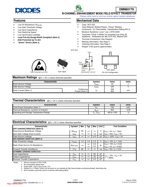
Features• Low On-Resistance: R DS(ON) • Low Gate Threshold Voltage • Low Input Capacitance • Fast Switching Speed• Low Input/Output Leakage• Lead Free By Design/RoHS Compliant (Note 2) • ESD Protected Up To 2kV • "Green" Device (Note 4)Mechanical Data• Case: SOT-523 • Case Material: Molded Plastic, “Green” MoldingCompound. UL Flammability Classification Rating 94V-0 • Moisture Sensitivity: Level 1 per J-STD-020D • Terminals: Finish ⎯ Matte Tin annealed over Alloy 42leadframe. Solderable per MIL-STD-202, Method 208 • Terminal Connections: See Diagram • Marking Information: See Page 3 • Ordering Information: See Page 3 • Weight: 0.002 grams (approximate)Maximum Ratings @T A = 25°C unless otherwise specifiedCharacteristicSymbol Value Units Drain-Source Voltage V DSS 60 VGate-Source Voltage V GSS±20 V Drain Current (Note 1) ContinuousPulsed (Note 3)I D300800mAThermal Characteristics @T A = 25°C unless otherwise specifiedCharacteristicSymbol Value Units Total Power Dissipation (Note 1)P D 150 mW Thermal Resistance, Junction to Ambient R θJA 833 °C/W Operating and Storage Temperature Range T J , T STG-65 to +150°CElectrical Characteristics @T A = 25°C unless otherwise specifiedCharacteristicSymbol Min Typ Max UnitTest ConditionOFF CHARACTERISTICS (Note 5) Drain-Source Breakdown Voltage BV DSS 60 ⎯ ⎯ V V GS = 0V, I D = 10μA Zero Gate Voltage Drain Current I DSS ⎯ ⎯ 1.0 μA V DS = 60V, V GS = 0V Gate-Source LeakageI GSS ⎯ ⎯ ±10 μA V GS = ±20V, V DS = 0V ON CHARACTERISTICS (Note 5) Gate Threshold VoltageV GS(th) 1.0 1.6 2.5 VV DS = 10V, I D = 1mA Static Drain-Source On-Resistance R DS (ON) ⎯ ⎯ ⎯ 2.0 3.0 ΩV GS = 10V, I D = 0.5A V GS = 5V, I D = 0.05A Forward Transfer Admittance |Y fs | 80 ⎯ ⎯ ms V DS =10V, I D = 0.2A DYNAMIC CHARACTERISTICS Input Capacitance C iss ⎯ ⎯ 50 pF V DS = 25V, V GS = 0V f = 1.0MHz Output CapacitanceC oss ⎯ ⎯ 25 pF Reverse Transfer CapacitanceC rss⎯⎯5.0pFNotes: 1. Device mounted on FR-4 PCB. 2. No purposefully added lead.3. Pulse width ≤10μS, Duty Cycle ≤1%4. Diodes Inc.’s “Green” policy can be found on our website at /products/lead_free/index.php.5. Short duration pulse test used to minimize self-heating effect.SOT-523TOP VIEWPin Out ConfigurationESD Protected up to 2kVEQUIVALENT CIRCUITPlease click here to visit our online spice models database.V , DRAIN-SOURCE VOLTAGE (V)Fig. 1 Typical Output CharacteristicsDS I , D R A I N C U R R E N T (A )DFig. 2 Typical Transfer CharacteristicsGS T , CHANNEL TEMPERATURE (°C)Fig. 3 Gate Threshold Voltage vs. Channel T emperaturech 00.51.5I DRAIN CURRENT (A)Fig. 4 Static Drain-Source On-Resistancevs. Drain CurrentD , R , S T A T I C D R A I N -S O U R CE D S (O N)Fig. 5 Static Drain-Source On-Resistancevs. Drain CurrentDR , S T A T I C D R A I N -S O U R C E D S (O N )V GATE SOURCE VOLTAGE (V)Fig. 6 Static Drain-Source On-Resistancevs. Gate-Source VoltageGS,R , S T A T I C D R A I N -S O U R C E O N -R E S I S T A N C E ()D S (O N )ΩFig. 7 CH Static Drain-Source On-State Resistancevs. Channel T emperatureR , S T A T I C D R A I N -S O U R C E D S (O N )1I , R E V E R S E D R A I N C U R RE N T (A )D R 1I , DRAIN CURRENT (A)D Fig.10 Forward Transfer Admittancevs. Drain CurrentOrdering Information (Note 6)Part Number Case Packaging DMN601TK-7SOT-523 3000/Tape & ReelNotes: 6. For packaging details, go to our website at /datasheets/ap02007.pdf.Marking InformationDate Code KeyYear 2005 2006 2007 2008 2009 2010 2011 2012 Code S T U V W X Y ZMonth Jan Feb Mar Apr May Jun Jul Aug Sep Oct Nov Dec Code 1 2 3 4 5 6 7 8 9 O N DK7K = Product Type Marking Code YM = Date Code Marking Y = Year (ex: S = 2005) M = Month (ex: 9 = September) K7K YMPackage Outline DimensionsSuggested Pad LayoutIMPORTANT NOTICEDiodes Incorporated and its subsidiaries reserve the right to make modifications, enhancements, improvements, corrections or other changes without further notice to any product herein. Diodes Incorporated does not assume any liability arising out of the application or use of any product described herein; neither does it convey any license under its patent rights, nor the rights of others. The user of products in such applications shall assume all risks of such use and will agree to hold Diodes Incorporated and all the companies whose products are represented on our website, harmless against all damages.LIFE SUPPORTDiodes Incorporated products are not authorized for use as critical components in life support devices or systems without the expressed written approval of the President of Diodes Incorporated.SOT-523Dim Min Max Typ A 0.15 0.30 0.22 B 0.75 0.85 0.80 C 1.45 1.75 1.60 D ⎯ ⎯ 0.50 G 0.90 1.10 1.00 H 1.50 1.70 1.60 J 0.00 0.10 0.05 K 0.60 0.80 0.75 L 0.10 0.30 0.22 M 0.10 0.20 0.12 N 0.45 0.65 0.50α0° 8° ⎯ All Dimensions in mmDimensions Value (in mm)Z1.8 X 0.4 Y 0.51 C 1.3 E 0.7X EYCZ分销商库存信息: DIODESDMN601TK-7。

MIC3003GFLFOM Management IC with Internal CalibrationMLF and MicroLead Frame are registered trademarks of Amkor Technology, Inc.General DescriptionThe MIC3003GFL is a fiber optic module controller which enables the implementation of sophisticated, hot-pluggable fiber optic transceivers with intelligent laser control and an internally calibrated Digital Diagnostic Monitoring Interface per SFF-8472. It essentially integrates all non-data path functions of an SFP/SFP+ transceiver into a tiny (3mm x 3mm ) MLF ® package. It also works well as a microcontroller peripheral in transponders or 10Gbps transceivers. The MIC3003GFL uses the same die as the MIC3003 with all its functions, but in a smaller package and different pin out. A highly configurable automatic power control (APC) circuit controls laser bias. Bias and modulation are temperature compensated using dual DACs, an on-chip temperature sensor, and NVRAM look-up tables. A programmable internal feedback resistor provides a wide dynamic range for the APC. Controlled laser turn-on.An analog-to-digital converter converts the measured temperature, voltage, bias current, transmit power, and received power from analog to digital. An EEPOT provides front-end adjustment of RX power. Each parameter is compared against user-programmed warning and alarm thresholds. Analog comparators and DACs provide fast monitoring of received power and critical laser operating parameters. Data can be reported as either internally calibrated or externally calibrated.An interrupt output, power-on hour meter, and data-ready bits add user friendliness beyond SFF-8472. The interrupt output and data-ready bits reduce overhead in the host system. The power-on hour meter logs operating hours using an internal real-time clock and stores the result in NVRAM.In addition to the features listed above, the MIC3003 features an extended temperature range, options to mask alarms and warnings interrupt and TXFAULT, a reset signal source, and the ability to support up to four chips with the same address on the serial interface. It also supports eight-byte SMBus block writes.Communication with the MIC3003 is via an industry standard 2-wire SMBus serial interface. Nonvolatile memory is provided for serial ID, configuration, and separate OEM and user scratchpad spaces.Datasheets and support documentation can be found on Micrel’s web site at: .Features• Packaged in a ultra small (3mm x 3mm) 24-pin MLF ® package • Extended temperature range• Alarms and warnings interrupt and TXFAULT masks • Capability to support up to four devices on one SMBus • APC or constant-current laser bias• Turbo mode for APC loop start-up and shorter laser turn on time • Supports multiple laser types and bias circuit topologies • Integrated digital temperature sensor• Temperature compensation of modulation, bias, bias fault and alarm thresholds via NVRAM look-up tables • NVRAM to support GBIC/SFP serial ID function • User writable EEPROM scratchpad• Reset signal compatible with some new systems requirements • Diagnostic monitoring interface per SFF-8472 – Monitors and reports critical parameters:temperature, bias current, TX and RX optical power, and supply voltage– S/W control and monitoring of TXFAULT, RXLOS, RATESELECT, and TXDISABLE – Internal or external calibration– EEPOT for adjusting RX power measurement • Power-on hour meter • Interrupt capability• Extensive test and calibration features • 2-wire SMBus-compatible serial interface • SFP/SFP+ MSA and SFF-8472 compliant • 3.0V to 3.6V power supply range • 5V-tolerant I/OApplications• SFP/SFP+ optical transceivers• SONET/SDH transceivers and transponders • Fibre Channel transceivers • 10Gbps transceivers• Free space optical communications • Proprietary optical linksTypical ApplicationOrdering InformationPart NumberPackage Marking Junction Temp.RangePackage Type Lead FinishMIC3003GFL GFL 3003 with Pb-Free bar-line indicator–45°C to +105°C24-pin (3mm x 3mm) MLF ® Pb-Free,NiPdAuMIC3003GFLTR (1) GFL 3003 with Pb-Free bar-line indicator–45°C to +105°C24-pin (3mm x 3mm) MLF ® Pb-Free,NiPdAuNote:1. Tape and Reel.ContentsGeneral Description (1)Features (1)Pin Configuration (8)Pin Configuration (8)Pin Description (MIC3003GFL only) (8)Absolute Maximum Ratings (10)Operating Ratings (10)Electrical Characteristics (10)Electrical Characteristics (12)Electrical Characteristics (13)Serial Interface Timing Diagram (14)Serial Interface Address Maps (15)Block Diagram (18)Analog-to-Digital Converter/Signal Monitoring (18)Alarms and Warnings Interrupt Source Masking (19)Alarms and Warnings as TXFAULT Source (21)Latching of Alarms and Warnings (21)SMBus Multipart Support (21)QGOP Pin Function (21)Calibration Modes (22)A/ External Calibration (22)Voltage (22)Temperature (22)Bias Current (22)TX Power (22)RX Power (23)B/ Internal Calibration (23)Computing Internal Calibration Results (23)C/ Reading the ADC Result Registers (25)RXPOT (25)Laser Diode Bias Control (25)Laser Modulation Control (26)Power On and Laser Start-Up (27)Fault Comparators (28)SHDN and TXFIN (29)Temperature Measurement (30)Diode Faults (30)Temperature Compensation (30)Alarms and Warning Flags (32)Control and Status I/O (32)System Timing (34)Warm Resets (36)Power-On Hour Meter (36)Test and Calibration Features (37)Serial Port Operation (38)Block Writes (38)Acknowledge Polling (39)Write Protection and Data Security (39)OEM Password (39)OEM Mode and User Mode (39)Detailed Register Descriptions (40)Alarm Threshold Registers (40)Temperature High Alarm Threshold (40)Temperature Low Alarm Threshold (40)Voltage High Alarm Threshold (40)D[7] read/write (40)Bias Current High Alarm Threshold (41)Bias Current Low Alarm Threshold (41)TX Optical Power High Alarm Threshold (41)TX Optical Power Low Alarm Threshold (42)RX Optical Power High Alarm Threshold (42)RX Optical Power Low Alarm Threshold (42)Warning Threshold Registers (43)Temperature High Warning Threshold (43)Temperature Low Warning Threshold (43)Voltage High Warning Threshold (43)Voltage Low Warning Threshold (44)Bias Current High Warning Threshold (44)Bias Current Low Warning Threshold (44)TX Optical Power High Warning (44)TX Optical Power Low Warning (45)RX Optical Power High Warning Threshold (45)RX Optical Power Low Warning Threshold (45)Checksum (CHKSUM) Checksum of bytes 0 - 94 at serial address A2h (45)ADC Result Registers (46)Temperature Result (46)Voltage (46)Laser Diode Bias Current (46)Transmitted Optical Power (47)Received Optical Power (47)Control and Status (CNTRL) (47)Application Select Control Mode (ASCM) (48)Alarm Flags (50)Alarm Status Register 0 (ALARM0) (50)Alarm Status Register 1 (ALARM1) (50)Warning Flags (51)Warning Status Register 0 (WARN0) (51)Warning Status Register 1 (WARN1) (51)Extended Control and Status (ECNTRL) (52)OEM Password Entry (OEMPW) (52)Power-On Hours (POHh and POHl) (53)Data Ready Flags (DATARDY) (53)User Control Register (USRCTL) (54)RESETOUT (54)OEM Configuration Register 0 (OEMCFG0) (55)OEM Configuration Register 1 (OEMCFG1) (56)OEM Configuration Register 2 (OEMCFG2) (57)APC Setpoint 0, 1, and 2 (APCSET0, APCSET1, APCSET2) Automatic Power Control Setpoint (58)Modulation Setpoint 0, 1, and 2 (MODSET0, MODSET1, and MODSET2) Nominal V MOD Setpoint (58)I BIAS Fault Threshold (IBFLT) Bias Current Fault Threshold (59)Transmit Power Fault Threshold (TXFLT) (59)Loss-Of-Signal Threshold (LOSFLT) (59)Fault Suppression Timer (FLTTMR) Fault Suppression Interval in Increments of 0.5 ms (60)Fault Mask (FLTMSK) (60)OEM Password Setting (OEMPWSET) (61)OEM Calibration 0 (OEMCAL0) (61)OEM Calibration 1 (OEMCAL1) (63)LUT Index (LUTINDX) (64)OEM Configuration 3 (OEMCFG3) (64)BIAS DAC Setting (APCDAC) Current VBIAS Setting (65)Modulation DAC Setting (MODDAC) Current VMOD Setting (66)OEM Readback Register (OEMRD) (66)OEM Configuration 4 (OEMCFG4) (67)OEM Configuration 5 (OEMCFG5) (68)OEM Configuration 6 (OEMCFG6) (69)Power-On Hour Meter Data (POHDATA) (70)OEM Scratchpad Registers (SCRATCHn) (71)RX Power Coefficient Look-up Table (RXLUTn) (71)Calibration Constants (CALCOEFn) (72)Manufacturer ID Register (MFG_ID) Identifies Micrel as the manufacturer of the device. Always returns 2Ah (72)Device ID Register (DEV_ID) (73)Package Information (74)Figure 1. MIC3003 Block Diagram (18)Figure 2. Analog-to-Digital Converter Block Diagram (18)Figure 3. Internal Calibration RX Power Linear Approximation (25)Figure 4. RXPOT Block Diagram (25)Figure 5. APC and Modulation Control Block Diagram (26)Figure 6. Programmable Feedback Resistor (26)Figure 7. Transmitter Configurations Supported by MIC3003 (26)Figure 8. V MOD Configured as Voltage Output with Gain (27)Figure 9. MIC3003 Power-On Timing (OE = 1) (28)Figure 10. Fault Comparator Logic (28)Figure 11. Saturation Detector (29)Figure 12. RXLOS Comparator Logic (29)Figure 14. Transmitter On-Off Timing (34)Figure 15. Initialization Timing with TXDISABLE Asserted (34)Figure 16. Initialization Timing with TXDISABLE Not Asserted (34)Figure 17. Loss-of-Signal (LOS) Timing (35)Figure 19. Successfully Clearing a Fault Condition (36)Figure 20. Unsuccessful Attempt to Clear a Fault (36)Figure 21. Write Byte Protocol (38)Figure 22. Read Byte Protocol (38)Figure 23. Read_Word Protocol (38)Figure 24. Eight-Byte Block Write Protocol (39)Table 1. Serial Interface Address Map, Device Address = A0h (15)Table 2. Serial Interface Address Map, Device Address = A2 (15)Table 3. Serial Interface Address Map (Temperature Compensation Tables), Device Address = A4h (16)Table 4. Serial Interface Address Map (OEM Configuration Registers), Device Address = A6h (17)Table 5. A/D Input Signal Ranges and Resolutions (19)Table 6. V AUX Input Signal Ranges and Resolutions (19)Table 7. Alarms Interrupt Sources Masking Bits (20)Table 8. Warnings Interrupt Sources Masking Bits (20)Table 9. RESETOUT Clear Delay (21)Table 10. LSB Values of Offset Coefficients (23)Table 11. Internal Calibration Coefficient Memory Map – Part I (24)Table 12. Internal Calibration Coefficient Memory Map – Part II (24)Table 13. Shutdown State of SHDN vs. Configuration Bits (27)Table 14. Shutdown State of V BIAS vs. Configuration Bits (27)Table 15. Shutdown State of V MOD vs. Configuration Bits (27)Table 16. Temperature Compensation Look-up Tables (30)Table 17. APC Temperature Compensation Look-Up Table (31)Table 18. I MOD Temperature Compensation Look-Up Table (31)Table 19. I BIAS Comparator Temperature Compensation Look-Up Table (31)Table 20. BIAS Current High Alarm Temperature Compensation Table (31)Table 21. MIC3003 Alarm and Warning Events (33)Table 22. Test and Diagnostic Features (37)Pin Configuration24-Pin MLF® (ML)Pin Description (MIC3003GFL only)Pin Number Pin Name Pin Function1 VDDD Power supply input for digital functions.Open-drain output. Can be selected (via OEMCFG3 bit 7) to be an open-drain GPO or an active-2 QGPOlow, open-drain, pulsed reset signal output controlled by the status of bits [0-2] of byte A2h: FFh.3 GNDD Ground return for digital functions.Digital input. Receiver Rate Select input. OR’ed with soft rate select bit SRS0 to determine the4 RS0state of the RRSOUT pin. The state of this pin is always reflected in the RS0S bit.If bit 4 (IE) in the USRCTL register is set to 0 (its default value), this pin is configured as an analog5 VIN/INTinput. If IE bit is set to 1, this pin is configured as an open-drain output.Analog input: Multiplexed A/D input for monitoring supply voltage, with a 0V to 5.5V input range.Open-drain output: outputs the internally generated active-low interrupt signal /INT.6 CLK Digital input. Serial clock input.7 DATA Digital I/O, open-drain, bi-directional serial data input/output.Digital input; Active high. The transmitter is disabled when this input is high or the STXDIS bit is8 TXDISABLEset to 1. The state of this input is always reflected in the TXDIS bit.Digital Output; Open-Drain, with programmable polarity. If OEMCFG5 bit 4 is set to 0, a high level9 TXFAULTindicates a hardware fault impeding transmitter operation. If OEMCFG5 bit 4 is set to 1, a low levelindicates a hardware fault impeding transmitter operation. The state of this pin is always reflectedin the TXFLT bit.Digital Input; Transmitter Rate Select Input; OR’ed with soft rate select bit SRS1 to determine the10 RS1state of the TRSOUT pin. The state of this pin is always reflected in the RS1S bit.Analog Input. Multiplexed A/D converter input for monitoring received optical power. The input11 VRXrange is 0 to V REF. A 5-bit programmable EEPOT on this pin provides coarse calibration andranging of the RX power measurement.Pin Number Pin Name Pin Function12 SHDN/TXFINDigital output/Input; programmable polarity. When used as shutdown output (SHDN), OEMCFG3bit 2 set to 0, SHDN is asserted at the detection of a fault condition if OEMCFG4 bit 7 is set to 0. IfOEMCFG4 bit 7 is set to 1, a fault condition will not assert SHDN. When programmed as TXFIN, itis an input for external fault signals to be OR’ed with the internal fault sources to drive TXFAULT.13 VILD+Analog Input. Multiplexed A/D input for monitoring laser bias current via a sense resistor (signalinput); accommodates inputs referenced to V DD or GND (see pin 14 description).14 VILD–Analog Input. Reference terminal for the multiplexed pseudo-differential A/D converter inputs formonitoring laser bias current via a sense resistor (VILD+ is the sensing input). Tie to V DD or GNDto reference the voltage sensed on VILD+ to V DD or GND, respectively.15 VDDA Power supply input for analog functions.16 GNDA Ground return for analog functions.17 VMPDAnalog Input. Multiplexed A/D converter input for monitoring transmitted optical power via amonitor photodiode. In most applications, VMPD will be connected directly to FB. The input rangeis 0 - V REF or 0 - V REF/4 depending upon the setting of the APC configuration bits18 FBAnalog Input. Feedback voltage for the APC loop op-amp. Polarity and scale are programmablevia the APC configuration bits I OEMCFG1. Connect to V BIAS if APC is not used.19 VMODAnalog Output. Buffered DAC output to set the modulation current on the laser driver IC. Operateswith either a 0– V REF or a (V DD–V REF) – V DD output swing so as to generate either a ground-referenced or a V DD referenced programmed voltage. A simple external circuit can be used togenerate a programmable current for those drivers that require a current rather than a voltageinput.20 VMOD–Analog input. This pin is the inverting terminal of the VMOD buffer op-amp. Connect to VMOD(gain = 1) or a feedback resistor network to set a different gain value.21 VBIASAnalog output. Buffered DAC output capable of sourcing or sinking up to 10mA under control ofthe APC function to drive an external transistor or the APCSET pin of a laser diode driver for laserdiode DC bias. The output and feedback polarity are programmable to accommodate either anNPN or a PNP transistor to drive a common-anode or common-cathode laser diode.22 COMPAnalog output. Compensation terminal for the APC loop. Connect a capacitor between this pin andGNDA or V DDA with the appropriate value to tune the APC loop time constant to a desirable value.23 RRSOUT/GPO Digital Output. Open-Drain or push-pull.If OEMCFG3 bit 4 is set to 0, RRSOUT is selected. It represents the receiver rate select as per SFF. This output is controlled by the SRS0 bit OR’ed with RS0 input and is open drain only.If OEMCFG3 bit 4 is set to 1, GPO is selected. General-purpose, non-volatile output, it is controlled by the GPO configuration bits in OEMCFG3.24 RXLOS/TRSOUT Digital output. This programmable polarity, open-drain outputs has two purposes:If OEMCFG6 bit 2 = 0, indicates the loss of the received signal as indicated by a level of received optical power below the programmed RXLOS comparator threshold; may be wire-OR’ed with external signals. Normal operation is indicated by a low level when OEMCFG6 bit 3 is set to 0 and a high level when OEMCFG6 bit 3 is set to 1. RXLOS is de-asserted when VRX > LOSFLTn. The LOS bit reflects the state of RXLOS whether driven by the MIC3003 or an external circuit.If OEMCFG6 bit 2 = 1, TRSOUT is selected. This signal represents the transmitter rate select as per the SFF specification. This output is controlled by the SRS1 bit OR’ed with the RS1 input.Absolute Maximum Ratings(1)Power Supply Voltage, V DD.......................................+3.8V Voltage on CLK, DATA, TXFAULT, VIN, RXLOS, TXDISABLE, RS0, RS1.........................–0.3V to +6.0V Voltage On Any Other Pin.....................–0.3V to V DD+0.3V Power Dissipation, T A = 85°C....................................1.5W Junction Temperature (T J).......................................150°C Storage Temperature (T S).......................–65°C to +150°C Soldering (20 sec.)...................................................260ºC ESD Ratings(3)Human Body Model..................................................2kV Machine Model.......................................................300V Operating Ratings(2)Power Supply Voltage, V DDA/V DDD...........+3.0V to +3.6V Ambient Temperature Range (T A) .......–40°C to +105°C Package Thermal ResistanceMLF® (θJA).................................................60°C/WElectrical CharacteristicsFor typical values, T A = 25°C, V DDA = V DDD = +3.3V, unless otherwise noted. Bold values are guaranteed for +3.0V ≤ (V DDA = V DDD)≤ 3.6V, T(min)≤ T A≤ T(min), (8)Symbol Parameter Condition Min Typ Max Units Power SupplyCLK = DATA = V DDD= V DDA; TXDISABLE low; all DACs at full-scale; all A/D inputs at full-scale; all other pins open. 2.3 3.5 mAI DD SupplyCurrentCLK = DATA = V DDD= V DDA; TXDISABLEhigh; FLTDAC at full-scale; all A/D inputsat full-scale; all other pins open.2.33.5 mAV POR Power-on Reset Voltage All registers reset to default values;A/D conversions initiated. 2.92.98 VVUVLOUnder-Voltage Lockout Threshold Note 5 2.5 2.73 VVHYSTPower-on Reset Hysteresis Voltage 170 mVtPORPower-on Reset Time V DD > V POR, Note 4 50 µs V REF ReferenceVoltage 1.2101.2251.240 V ΔV REF/ΔV DDAVoltage Reference Line Regulation 1.7 mV/V Temperature-to-Digital Converter CharacteristicsLocal Temperature MeasurementError–40°C ≤ T A≤ +105°C, Note 6 ±1 ±3 °Ct CONV Conversion Time Note 4 60 mst SAMPLE SamplePeriod 100 ms Voltage-to-Digital Converter Characteristics (V RX, V AUX, V BIAS, V MPD, V ILD±)Voltage Measurement Error –40°C ≤ T A≤ +105°C, Note 6 ±1 ±2.0 %fst CONV Conversion Time Note 4 10 mst SAMPLE Sample Period Note 4 100 ms Notes:1. Exceeding the absolute maximum rating may damage the device.2. The device is not guaranteed to function outside its operating rating.3. Devices are ESD sensitive. Handling precautions recommended. Human body model, 1.5k in series with 100pF.4. Guaranteed by design and/or testing of related parameters. Not 100% tested in production.5. The MIC3003 will attempt to enter its shutdown state when V DD falls below V UVLO. This operation requires time to complete. If the supply voltage fallstoo rapidly, the operation may not be completed.6. Does not include quantization error.分销商库存信息:MICRELMIC3003GFL MIC3003GFL TR。

NOIH2SM1000AHAS2 Image SensorINTRODUCTIONScopeThis ICD version is generated after qualification campaign closure. This specification details the ratings, physical, geometrical, electrical and electro-opticalcharacteristics, and test- and inspection-data for the High Accuracy Star Tracker (HAS2) CMOS active pixel image sensor (CMOS APS).The device described in this document is protected by US patent 6,225,670 and others.Component Type ValuesTable 10 on page 8 provides a summary of the type variants of the basic CMOS image sensor. The complete list of specifications for each type variant is given in Detailed Specifications on page 9.All specifications in Detailed Specifications on page 9 are given at 25 ±3°C, under nominal clocking and bias conditions. Exceptions are noted in the ‘Remarks’ field. Maximum RatingTable 11 on page 9 specifies the maximum ratings. Do not exceed these ratings at any times, during use or storage. Physical Dimension and Geometrical Information Figure 2 on page 24 shows the physical dimensions of the assembled component. The geometrical information in Figure 4 on page 25 describes the position of the die in the package.Pin AssignmentFigure 5 on page 26 contains the pin assignment. The figure contains a schematic drawing and a pin list. A detailed functional description of each pin is available in Pin List on page 36.Soldering InstructionsSoldering is restricted to manual soldering only. No wave or reflow soldering is allowed. For manual soldering, the following restrictions are applicable:•Solder 1 pin on each of the four sides of the sensor.•Cool down for a minimum period of 1 minute before soldering another pin on each of the four sides.•Repeat soldering of 1 pin on each side, including a 1 minute cool down period.Handling PrecautionsThe component is susceptible to damage by electro-static discharge. Therefore, use suitable precautions for protection during all phases of manufacture, testing, packaging, shipment, and any handling. Follow these guidelines:•Always manipulate devices in an ESD controlled environment.•Always store the devices in a shielded environment that protects against ESD damage (at least a non-ESD generating tray and a metal bag).•Always wear a wrist strap when handling the devices and use ESD safe gloves.•The HAS2 is classified as class 1A (JEDEC classification - [AD03]) device for ESD sensitivity. For proper handling and storage conditions, refer to the ON Semiconductor application note AN52561.Limited WarrantyON Semiconductor’s Image Sensor Business Unit warrants that the image sensor products to be delivered hereunder, if properly used and serviced, will conform to Seller’s published specifications and will be free from defects in material and workmanship for two (2) years following the date of shipment. If a defect were to manifest itself within two (2) years period from the sale date, ON Semiconductor will either replace the product or give credit for the product.Return Material Authorization (RMA)ON Semiconductor packages its image sensor products in a clean room environment under strict handling procedures and ships all image sensor products in ESD-safe, clean-room-approved shipping containers. Products returned to ON Semiconductor for failure analysis should be handled under these same conditions and packed in its original packing materials, or the customer may be liable for the product.Storage InformationThe components must be stored in a dust-free and temperature-, humidity-and ESD-controlled environment.•Store devices in special ESD-safe trays such that the glass window is never touched.•Close the trays with EDS-safe rubber bands.•Seal the trays in an ESD-safe conductive foil in clean room conditions.•For transport and storage outside a clean room, pack the trays in a second ESD-save bag that is sealed in cleanroom.Additional InformationThe HAS sensor is subject to the standard European export regulations for dual use products. A Certificate of Conformance will be issued upon request at no additional charge. The CoC refers to this document. Additional screening tests is done on request at additional cost.The following data is delivered by default with FM sensors:•Sensor calibration data •Temperature calibration data •Certificate of Conformance to this detailed specification•Visual inspection report•Bad pixel mapITAR InformationThe NOIH2SM1000A is an ITAR-free component.Table 1. ORDERING INFORMATIONMarketing Part Number Description Package NOIH2SM1000T-HHC HAS2 Mono, Flight Model, Level 284-pin JLCC NOIH2SM1000A-HHC HAS2 Mono, Engineering ModelNOIH2SM1000S-HHC HAS2 Mono, Flight Model, Level 1NOIH2SM1000A-HWC HAS2 Mono Windowless, Engineering ModelNOIH2SM1000S-HWC HAS2 Mono Windowless, Flight Model, Level 1ORDERING CODE DEFINITIONO = OptoN = ON SemiconductorHAS2M=MonoH= JLCCCommercial Temperature Range 1000M HS = Standard Process1.0 MP Resolution A= Engineering Model H= BK7G18 GlassI I = Image Sensors H CN O H2S A −S= Flight Model, Level 1T= Flight Model, Level 2W= WindowlessAPPLICABLE DOCUMENTSThe following documents form part of this specification:Table 2. APPLICABLE DOCUMENTSNo.Reference Title Issue DateAD01ESCC Generic Specification 9020Charge Coupled Devices, Silicon, Photosensitive2March 2010AD02001-06225(Note 1)Electro-optical test methods for CMOS image sensors E October, 2008AD03JESD22-A114-B Electrostatic Discharge (ESD) Sensitivity Testing HumanBody Model (HBM)B June, 2000AD04APS2-FVD-06-003Process Identification Document for HAS22February, 2008 AD05001-49283Visual Inspection for FM devices1January, 2008 AD06001-49280HAS2 FM Screening2June, 20091.This specification will be superseded by the ESCC basic specification 25000, which is currently under development. The current referenceis an internal ON Semiconductor procedure and is a confidential document.2.Lot acceptance and screening are based on ESCC 9020 issue 2. Please note that Lot Acceptance and Screening on page 6 − is valid forthe Flight Model Level 1 devices. For more information on Flight Model 1 Windowless devices, please contact imagesensors@DETAILED INFORMATIONDeviations from Generic SpecificationLot acceptance and screening are based on ESCC 9020 issue 2. See Lot Acceptance and Screening on page 6 for more information.Mechanical RequirementsDimension CheckThe dimensions of the components specified here is checked and must comply with the specifications and the tolerances indicated in Figure 2 on page 24 Geometrical CharacteristicsThe geometrical characteristics of the components specified here is checked and must comply with the specifications and tolerances given in Figure 2 on page 24 and Figure 3 on page 25WeightThe maximum weight of the components specified here is specified in Table 14 on page 9Materials and FinishesThe materials and finishes is as specified in this document. Where a definite material is not specified, a material which enables the components to meet the performance requirements of this specification must be used. See Note 2. CaseThe case is hermetically sealed and must have a ceramic body and a glass window.Table 3. CASEType JLCC−84Material Black Alumina BA−914 Thermal expansion coefficient7.6 x 10−6/KHermeticity< 5 x 10⁻⁷ atms. cm3/s Thermal resistance(Junction to case)3.633°C/WLead Material and FinishTable 4. LEAD MATERIAL AND FINISHLead Material KOVAR1e Finish Nickel, min 2 m m2nd Finish Gold, min 1.5 m mWindowThe window material is a BK7G18 glass lid with anti-reflective coating applied on both sides.The optical quality of the glass must have the specifications in Table 15 on page 9.The anti reflective coating has a reflection coefficient less than 1.3% absolute and less than 0.8% on average, over a bandwidth from 440 nm to 1100 nm.Level 2 versus Level 1 differencesHAS2 Level 2 devices are differing from Level 1 devices in Lot Acceptance and Screening on page 6•100% screening is applied with burn-in limited to 168 hinstead of 240 h as for Level 1.•Assembly process is based on ESA qualified process (same procedures and materials)•Devices will be fully tested at room temperature, electrical testing at 85 degrees is limited to power consumption measurements only.•X/Y dye placement is relaxed to +/- 200 m m.•Mismatching between odd and even columns in Direct Readout is allowed but shall stay in the limit of127LSB.•The defect and particles specification will be the same as for the Engineering Model - NOIH2SM1000A-HHC – with the exception of the defective columns which are not allowed in the Level 2 devices. Refer to Table 10“Type Variant Summary” on page 8.•Endurance testing during wafer LAT is limited to a 1000 h burn in instead of 2000 h and will be performed on 3 un-screened parts instead of 6.•Prior to endurance testing and total dose testing, a stabilization bake of 48 hrs, followed by a 168 hrs burn-in, shall be performed.•During wafer LAT, the Electro-optical measurements is limited on 2 parts (1 from endurance testing and 1 from radiation testing) instead of 6.•For each assembly batch (manufacturing-lot), 2 screened devices will be made available for a DPA test. An assembly batch is defined as a group of parts which have been assembled within a time window of less than one week. The DPA devices can be rejected devices (glass lid cosmetic defects, electrical defects,…) but has to be screened through the same thermal steps as the HAS2 “level2”. The DPA test will be carried out by ON Semiconductor as a customer courtesy.Prior to DPA testing, the following tests are performed: Solderability and Resistance to Solvents (marking permeability).NOTE:As the glass lid removal is a best effort activity, the DPA test cannot be 100% guaranteed.•Pictures and defect maps are not included in the data pack, but will be made available upon request.•Assembly lot acceptance testing is not performed.Data PackEach set of devices will have a data pack which will be made available to the customer. The data pack consists of:•CoC form referring to the applicable specification •Calibration data •Screening Report•Life Test Report and Radiation (Total Dose) Test Report for each wafer lot •Electrical Test Report •Spectral response data •Visual Inspection Report •DPA Test ReportMarkingGeneralThe marking must consist of lead identification and traceability information.Lead IdentificationAn index to pin 1 must be located on the top of the package in the position defined in Figure 2 on page 24. The pin numbering is counter clock-wise, when looking at the top-side of the component.Traceability InformationEach component must be marked such that complete traceability is maintained.The component must have a number as follows:Figure 1. Product MarkingXXXXX = Specific Device Code A = Assembly Location WL = Wafer Lot YY = YearWW = Work WeekNNNN = Serial NumberTable 5. PACKAGE MARK DECODEROrderable Part Number Package Mark: Line 1Package Mark: Line 2Package Mark: Line 3NOIH2SM1000T-HHC NOIH2SM1000T -HHC_NNNN AWLYYWW NOIH2SM1000A-HHC NOIH2SM1000A -HHC_NNNN AWLYYWW NOIH2SM1000S-HHC NOIH2SM1000S -HHC_NNNN AWLYYWW NOIH2SM1000A-HWC NOIH2SM1000A -HWC_NNNN AWLYYWW NOIH2SM1000S-HWCNOIH2SM1000S-HWC_NNNNAWLYYWWwhere NNNN- serialized number controlled manually by ON Semiconductor, BELGIUM where DD-MM-YYYY represents the lot assembly date NOIH2SM1000T-HHC has a Minimum Order Quantity of 10Electrical and Electro −optical MeasurementsElectrical and Electro −optical Measurements at Reference TemperatureThe parameters to be measured to verify the electrical and electro-optical specifications are given in Table 18 on page 13 and Table 27 on page 23. Unless otherwise specified, the measurements must be performed at a environmental temperature of 22 ±3°C.For all measurements, the nominal power supply, bias,and clocking conditions apply. The nominal power supply and bias conditions are given in Table 28 on page 23; thetiming diagrams in Figure 35 on page 47 and Figure 37 on page 49.NOTE:The given bias and power supply settings implythat the devices are measured in ‘soft-reset’condition.Electrical and Electro −optical Measurements at High and Low TemperatureTable 19 on page 14 and Table 20 on page 15 list the parameters to be measured to verify electrical and electro-optical specifications. Unless otherwise specified,the measurements must be performed at –40 (–5 +0) °C and at +85 (+5 –0) °C.Circuits for Electrical and Electro−optical Measurements Circuits for performing the electro−optical tests in Table18 on page13 and Table 27 on page 23 are shown in Figure 49 on page 59 to Figure 52 on page 59.Burn−in TestParameter Drift ValuesThe parameter drift values for power burn-in are specified in Table 21 on page 17. Unless otherwise specified, the measurements must be conducted at an environmental temperature of 22 ±3°C and under nominal power supply, bias, and timing conditions.Do not exceed the parameter drift values. In addition to these drift value requirements, do not exceed the limit values of any parameter, as indicated in Table 18 on page13 Conditions for High Temperature Reverse Bias Burn-in Not ApplicableConditions for Power Burn-inThe conditions for power burn-in is specified in Table 24 on page 19 of this specification.Electrical Circuits for High Temperature Reverse Bias Burn-inNot ApplicableElectrical Circuits for Power Burn-inCircuits to perform the power burn-in test are shown in Figure 48 on page 58 and Figure 49 on page 59 of this specification.Environmental and Endurance TestsElectrical and Electro-optical Measurements on Completion of Environmental TestThe parameters to be measured on completion of environmental tests are listed in Table 25 on page 20. Unless otherwise stated, the measurements must be performed at a environmental temperature of 22 ±3°C. Measurements of dark current must be performed at 22 ±1°C and the actual environmental temperature must be reported with the test results.Electrical and Electro-optical Measurements At Intermediate Point During Endurance TestThe parameters to be measured at intermediate points during endurance test of environmental tests are listed in Table 25 on page 20. Unless otherwise stated, the measurements must be performed at an environmental temperature of 22 ±3°C.Electrical and electro-optical Measurements on Completion of Endurance TestThe parameters to be measured on completion of endurance tests are listed in Table 25 on page 20. Unless otherwise stated, the measurements must be performed at a environmental temperature of 22 ±3°C.Conditions for Operating Life TestThe conditions for operating life tests must be as specified in Table 24 on page 19 of this specification.Electrical Circuits for Operating Life TestCircuits for performing the operating life test are shown in Figure 49 on page 59 and next ones of this specification. Conditions for High Temperature Storage TestThe temperature to be applied must be the maximum storage temperature specified in Table 11 on page 9 of this specification.Total Dose Radiation TestApplicationThe total dose radiation test must be performed in accordance with the requirements of ESCC Basic Specification 22900.Parameter Drift ValuesThe allowable parameter drift values after total dose irradiation are listed in Table 22 on page 18 . The parameters shown are valid after a total dose of 42 KRad and 168h/100°C annealing.Bias ConditionsContinuous bias must be applied during irradiation testing as shown in Figure 49 on page 59 and next ones of this specification.Electrical and Electro-optical MeasurementsThe parameters to be measured, prior to, during and on completion of the irradiation are listed in Table 27 on page23 of this specification. Only devices that meet the specification in Table 18 on page 13 of this specification must be included in the test samples.Lot Acceptance and ScreeningThis section describes the Lot Acceptance Testing (LAT) and screening on the HAS2 FM devices. All tests on device level must be performed on screened devices (see Table 9 on page 7)Wafer Lot AcceptanceThis is the acceptance of the silicon wafer lot. This must be done on every wafer lot that is used for the assembly of flight models.Table 6.Test Test Method Number of Devices Test Condition Test Location Wafer processingdata reviewPID NA NA ON Semiconductor SEM ESCC 21400 4 naked dies NA Test houseTotal dose test ESCC 22900 3 devices42 krad, not to exceed3.6 krad/hr Test house by ON SemiconductorEndurance test MIL-STD-883 Method 1005 6 devices2000h at +125°C Test houseBefore and after total dose test and endurance test:•Electrical measurements before and after at high, low, and room temperature. See Table 18 on page13, Table 19 on page 14 and Table 20 on page 15 of this specification.•Visual inspection before and after•Detailed electro-optical measurements before and after Glass Lot AcceptanceTransmission and reflectance curves that are delivered with each lot must be compared with the specifications in Table 15. Three glass lids are chosen randomly from the lot and measured in detail. The results are compared with Figure 5 on page 26.Package Lot Acceptance•Five packages are chosen randomly from the lot and measured in detail. The results are compared with Figure 2 on page 24.•A solderability test is covered in the assembly lot acceptance tests (Table 7)Table 7. ASSEMBLY LOT ACCEPTANCETest Test Method Number ofDevices Test Condition Test LocationSpecial assembly house inprocess controlAssembly House Bond strength test MIL-STD-883 method 20112D Assembly HouseAssembly house geometrical datareviewReview All CYSolder ability MIL-STD883, method 20033D Test House Terminal strength MIL-STD 883, method 2004Marking permanence ESCC 24800Geometrical measurements PID All CY Temperature cycling MIL-STD 883, method 10105Condition B50 cycles–55°C / +125°CTest House Moisture resistance JEDEC Std. Method A101-B240 h at 85°C / 85%Test HouseTable 7. ASSEMBLY LOT ACCEPTANCETestTest LocationTest ConditionNumber of DevicesTest MethodDPADie shear test MIL-STD-883 method 20194N/A Test House Bond pull testMIL-STD-883 method 2011All wiresTest HouseNOTE:As the glass lid is removed from the packageprior to DPA, the results of the DPA cannot be guaranteed.Before and after the following tests are done:•Electrical measurements conform to Table 18 on page 13 of this specification •Detailed visual inspection •Fine leak test + gross leak testFine- and gross-leak tests must be performed using the following methods:Fine Leak test : MIL-STD-883, Test Method 1014,Condition AGross Leak test : MIL-STD-883, Test Method 1014,Condition CThe required leak rate for fine leak testing is 5x 10⁻⁷atms.cm 3/sTable 8. PERIODIC TESTINGTestTest MethodNumber of DevicesTest ConditionTest Location Mechanical shock MIL-STD 883, method 20022 B - 5 shocks, 1500 g – 0.5 ms – ½ sine, 6 axesTest House Mechanical vibration MIL-STD 883, method 20072A - 4 cycles, 20 g 80 to 2000 Hz, 0.06 inch 20 to 80 Hz, 3 axesTest HouseDPADie shear test MIL-STD-883 method 20192N/A Test House Bond pull testMIL-STD-883 method 2011All wiresTest HouseNOTE:As the glass lid is removed from the packageprior to DPA, the results of the DPA cannot be guaranteed.Periodic testing is required every two years. Before and after the following tests are done:•Electrical measurements conform to Table 18 on page 13•Detailed visual inspection •Fine leak test + gross leak testFine- and gross-leak tests must be performed using the following methods:Fine Leak Test : MIL-STD-883, Test Method 1014,Condition AGross Leak Test : MIL-STD-883, Test Method 1014,Condition CThe required leak rate for fine leak testing is 5x 10⁷atms.cm 3/sTable 9. SCREENINGNo.TestTest MethodNumber of DevicesTest Condition Test Location 1HCRT Electrical measurements001-53958AllHT +85°C LT –40°C RT +25°CON Semiconductor2Visual inspection001-49283 + ICD All ON Semiconductor 3Die placement measurements Internal proc.All ON Semiconductor 4XRAYESCC 20900All Test House 5Stabilization bake MIL-STD-883 method 1008All 48h at 125°C Test House 6Fine leak testMIL-STD-883 method 1014AllATest HouseTable 9. SCREENING7Gross leak test MIL-STD-883 method 1014All C Test HouseTest House 8Temperature cycling MIL-STD-883 method 1010All B - 10 cycles–55°C +125°C 9Biased Burn-in ICD All240 h at +125°C ON Semiconductor 10Mobile Particle Detection MIL-STD-883 method 2020All A Test House 11Fine leak test MIL-STD-883 method 1014All A Test House 12Gross leak test MIL-STD-883 method 1014All C Test HouseON Semiconductor 13HCRT Electrical measurements001-53958All HT +85°CLT –40°CRT +25°C 14Final Visual Inspection001-49283 + ICD All ON SemiconductorTABLES AND FIGURESSpecification TablesTable 10. TYPE VARIANT SUMMARYHAS2 Type Variants Engineering Model Flight Model Optical quality (see Optical Quality − Definitions on page 67)Dead pixels10020Bright pixels in FPN image5020Bad pixels in PRNU image15050Bad columns50Bad rows50Bright pixel clusters2 adjacent bright pixels2524 or more adjacent bright pixels100DSNU defects at 22 dec BOL12001000DSNU defects at 22 dec EOL15001250 Particle contaminationFixed particles outside focal plane N/A N/AMobile particles > 20 m m00Fixed particles on focal plane > 20 m m00Mobile particles > 10 m m and < 20 m m2010Fixed particles on focal plane > 10 m m and < 20 m mParticles < 10 m m N/A N/AWafer lot acceptance (see section Wafer Lot Acceptance on page 6)NO YesGlass lot acceptance (see section Glass Lot Acceptance on page 6)NO Yes Assembly lot acceptance (Table 7 on page 6)NO Yes Periodic testing (Table 8 on page 7)NO Yes Screening (Table 9 on page 7)NO Yes Calibration data NO YesVisual Inspection + particle mapping NO YesTable 11. MAXIMUM RATINGSNo.Characteristic Min Typ Max Unit Remarks1Any supply voltage except VDD_RES–0.5 3.3+7.0V2Supply voltage at VDD_RES–0.5 3.3+5.0V 3.3 V for normal operation; up to5V for increased full well capacity.3Voltage on any input terminal–0.5 3.3Vdd + 0.5V4Soldering temperature NA NA260°C Hand soldering only; See Solder-ing Instructions on page 1 5Operating temperature–40NA+85°C6Storage temperature–55NA+125°CStresses exceeding Maximum Ratings may damage the device. Maximum Ratings are stress ratings only. Functional operation above the Recommended Operating Conditions is not implied. Extended exposure to stresses above the Recommended Operating Conditions may affect device reliability.Detailed Specifications − All Type VariantsTable 12. GENERAL SPECIFICATIONSNo.Characteristic Min Typ Max Unit Remarks1Image sensor format N/A1024 x 1024N/A pixels2Pixel size N/A18N/A m m3ADC resolution N/A12N/A bit10-bit accuracy at 5 Msamples/secTable 13. SILICON PARTICLE CONTAMINATION SPECIFICATIONSNo.Characteristic Min Typ Max Unit Remarks1Optical quality: Particle max size N/A N/A20m m See Type Variant Summary onpage 8Table 14. MECHANICAL SPECIFICATIONSNo.Characteristic Min Typ Max Unit Remarks1a Flatness of image area NA7.4NA m m Peak-to-peak at 25 ±3°CSpecified by the foundry over anentire 8-inch wafer 1b Flatness of glass lid NA90150m m Towards ceramic package2Mass7.77.858.0g3Total thickness 3.2 3.3 3.4mm Package + epoxy + glass lid4a Die position, X offset NA NA0.1mm Die in center of cavity4b Die position, Y offset NA NA0.1mm Die in center of cavity5Die position, parallelism vs window Die position, parallelism vs backside –0.10.10.10.1mm6Die position, Y tilt–0.100.1°7Die position, X tilt–0.100.1°8Die – window distance0.250.30.35mmTable 15. GLASS LID SPECIFICATIONSNo.Characteristic Min Typ Max Unit Remarks 1a XY size26.7 x 26.726.8 x 26.826.9 x 26.9mm1b Thickness 1.4 1.5 1.6mmTable 15. GLASS LID SPECIFICATIONSNo.RemarksUnitMaxTypMinCharacteristic2a Spectral range for optical coating ofwindow440NA1100nm2b Reflection coefficient for window NA<0.8<1.3%Over bandwidth indicated in 2a3Optical quality:Scratch max widthScratch max numberDig max sizeDig max number N/A N/A1056025m mTable 16. ENVIRONMENTAL SPECIFICATIONSNo.Characteristic Min Typ Max Unit Remarks1Operating temperature–40NA+85°C2Storage temperature–55NA+125°C Lower storage temperatures (up to–80°C) have been tested and thedevice survives, but this is not afully qualified temperature.3Sensor total dose radiation tolerance N/A42N/A krad (Si)Tested for functionality up to300krad, 42 krad is guaranteed4Sensor SEL threshold with ADC enabled NA NA>110MeV cm3mg-1Equivalent LET valueTable 17. ELECTRICAL SPECIFICATIONSNo Characteristic Min Typ Max Unit Remarks1Total power supply current stand-by1618.521mA2Total power supply current, operational353740mA ADC at 5 MHz sampling ratemeasured3Power supply current to ADC, operational: analog + digital 171921mA ADC at 5 MHz sampling ratemeasured4Power supply current to image core,operational1415.517mA5Input impedance digital input3NA NA M W6Input impedance ADC input3NA NA M W7Output amplifier voltage range 2.2 2.45 2.6V8Output amplifier gain setting 0NA1NA–Nominal 1measured reference9Output amplifier gain setting 1 1.9 2.1 2.3–Nominal 2relative to setting 010Output amplifier gain setting 2 3.8 4.1 4.4–Nominal 4relative to setting 011Output amplifier gain setting 37.27.78.2–Nominal 8relative to setting 012Output amplifier offset setting 00.860.93 1.0V0 decodes to middle value 13Output amplifier offset setting 31 1.30 1.35 1.40V14Output amplifier offset setting 320.430.510.6V15Output amplifier offset setting 630.800.90 1.0V16ADC ladder network resistance NA 1.8NA k W Typical value17ADC differential nonlinearity NA711lsb18ADC integral nonlinearity NA818lsb分销商库存信息: ONSEMINOIH2SM1000S-HHC。

目录1 总则 (3)2 电制 (3)3 电源设备 (4)4 配电设备 (6)5 动力装置 (9)6 照明系统 (10)7 无线电设备 (12)8 导航、助航系统 (13)9 火灾报警装置 (14)10 生活、娱乐设施 (15)11 电缆 (15)12 接地 (16)1 总则1.1 本船电气设计的主要依据:1)《钢质海洋渔船建造规范》(1998年)2)《渔业船舶法定检验规则》(2000年)及修改通报3) 设计任务书及有关要求。
总长:39.20m垂线间长:35.00m航区:近海1.2 国产的电气设备应符合“ZY”规范或“GB”标准的有关要求,进口的电气设备应经“ZY”或按IEC要求及制造厂标准。
1.3电气设备的备品备件按如下原则提供:国产的电气设备按“ZY”规范的有关要求。
进口的电气设备按制造厂标准。
1.4电气设备的制造厂试验一般根据“ZY”规范和制造厂的标准进行,船厂试验的细节根据设计所的试验大纲。
1.5 电气设备安装,除特殊要求外,均按:“船舶电气设备安装工艺(CB/T3909-1999)”进行。
2 电制2.1 动力装置采用AC380V 50HZ 3相3线制。
2.2 照明及小型电气装置采用:AC220V 50HZ单相2线制(主电路为3相3线制)。
2.3 通信助航设备采用:1)AC220V 50HZ 单相2线制。
2)DC24V 2线制。
2.4 应急、低压照明系统采用:DC24V双线绝缘制。
3 电源设备3.1交流发电机组1)发电设备机舱设交流发电机组2台,作船上动力和照明设备、通信设备等用电。
该机组原则上使用一台,另一台为备用。
NO.1-2发电机组型式:防滴自通风型功率: 40KW电流: 72.2A电压: AC400V相数: 3相线制: 3线极数: 4极频率: 50HZ转速: 1500r/min功率因数:0.8工作方式:全负荷连续运行绝缘等级:F级励磁方式:自励式驱动方式:辅机驱动防护等级:IP22制造商:国产上述2台发电机可实现短时并车实现负载转移。

description :A mmB mm Cmm D mm Emm= Start of winding Marking = Inductance codeEigenschaften / properties Wert / valueEinheit / unittol.Induktivität /inductanceDC-Widerstand /DC-resistance DC-Widerstand /DC-resistance Nennstrom /rated currentSättigungsstrom /saturation current Eigenres.-Frequenz /self-res.-fequency33% Umgebungstemperatur / temperature:+20°CFerrit Endoberfläche / finishing electrode:CZ10-08-01ME 09-01-15MST 08-04-11MST 04-10-11MST04-08-09MPH03-03-20Name Datum / dateKunde / customerFreigabe erteilt / general release:C Lötpad / soldering spec.:B Elektrische Eigenschaften / electrical properties:E Testbedingungen / test conditions:Luftfeuchtigkeit / humidity:It is recommended that the temperature of the part does F Werkstoffe & Zulassungen / material & approvals:Draht / wire:Class HG Eigenschaften / general specifications:Betriebstemp. / operating temperature: -40°C - + 125°C Sn/Ag/Cu - 96.5/3.0/0.5%DATUM / DATE : 2010-08-01max.mA Datum / date.................................................................................Unterschrift / signature Kontrolliert / approvedTestbedingungen / test conditions D-74638 Waldenburg · Max-Eyth-Strasse 1 - 3 · Germany · Telefon (+49) (0) 7942 - 945 - 0 · Telefax (+49) (0) 7942 - 945 - 400Geprüft / checked SRFMHzUmgebungstemp. / ambient temperature: -40°C - + 85°C Basismaterial / base material:not exceed 125°C under worst case operating conditions.POWER-CHOKE WE-TPCA Mechanische Abmessungen / dimensions:1,60 typ.1,60typ.2,8 ± 0,2HP 34401 A für/for R DC und I DC0,028± 30%2,20µH2350R DC typ 0,023I DC D Prüfgeräte / test equipment:HP 4274 A für/for L und/and Q @ 20°C @ 20°C ∆T=30 K 100 kHZ / 0,1V2500100,0I sat |ΔL/L|<35%Version 5.....................................................................................................................................................................................................................................................Würth Elektroniktyp.R DC max typ.L max.mA typ.Version 44,8 ± 0,24,8 ± 0,2Type 4828Änderung / modificationVersion 1Version 2Version 3Version 6[mm]5,302,001,502,001,80MarkingABCDDEdescription :CZ10-08-01ME 09-01-15MST 08-04-11MST 04-10-11MST04-08-09MPH03-03-20Name Datum / dateFreigabe erteilt / general release:Kontrolliert / approvedDATUM / DATE : 2010-08-01Würth ElektronikKunde / customer...................................................................................................................................................................POWER-CHOKE WE-TPCH Induktivitätskurve / Inductance curve :Version 4Version 5Änderung / modificationVersion 1Version 2Version 3D-74638 Waldenburg · Max-Eyth-Strasse 1 - 3 · Germany · Telefon (+49) (0) 7942 - 945 - 0 · Telefax (+49) (0) 7942 - 945 - 400Datum / dateUnterschrift / signature Version 6 ...................................................................................................................................................................Geprüft / checked 0,000,501,001,502,002,500,000,501,001,502,002,503,003,50L (µH )Current (A)Induktivität vs Strom (typ.) / Inductance vs Current (typ.)description :I Rollenspezifikation / tape and reel specification:A 8,0± 1,0mm B4,00± 0,1mma 178± 0,5mmb 20,20± 0,1mm+ 0,5- 1,0d 50,0± 1,0mmCZ10-08-01ME 09-01-15MST 08-04-11MST 04-10-11MST04-08-09MPH03-03-20Name Datum / dateWürth Elektronik...................................................................................................................................................................Würth Elektronik eiSos GmbH & Co.KGD-74638 Waldenburg · Max-Eyth-Strasse 1 - 3 · Germany · Telefon (+49) (0) 7942 - 945 - 0 · Telefax (+49) (0) 7942 - 945 - 400Geprüft / checked Kontrolliert / approvedÄnderung / modification...................................................................................................................................................................Datum / dateUnterschrift / signature Gurtspezifikation / Tape specification: Rollenspezifikation / Reel specification:Freigabe erteilt / general release:Kunde / customermm 13,00POWER-CHOKE WE-TPCDATUM / DATE : 2010-08-01Version 5c Version 1Version 2Version 3Version 4Version 6Ø cadbThe force for tearing off cover tape is 20 to 70 grams in arrow direction150feeding directionThis electronic component has been designed and developed for usage in general electronic equipment. Before incorporating this component into any equipment where higher safety and reliability is especially required or if there is the possibility of direct damage or injury to human body, for example in the range of aerospace, aviation, nuclear control, submarine, transportation, (automotive control, train control, ship control),transportation signal, disaster prevention, medical, public information network etc, Würth Elektronik eiSos GmbH must be informed before the design-in stage. In addition, sufficient reliability evaluation checks for safety must be performed on every electronic component which is used in electrical circuits that require high safety and reliability functions or performance.分销商库存信息: WURTH-ELECTRONICS 7440430022。

8-/6-/4-Channel DAS with 16-Bit, BipolarInput, Simultaneous Sampling ADCData SheetAD7606/AD7606-6/AD7606-4Rev. CInformation furnished by Analog Devices is believed to be accurate and reliable. However , no responsibility is assumed by Analog Devices for its use, nor for any infringements of patents or other rights of third parties that may result from its use. Specifications subject to change without notice. No license is granted by implication or otherwise under any patent or patent rights of Analog Devices. T rademarks and registered trademarks are the property of their respective owners.One Technology Way, P.O. Box 9106, Norwood, M A 02062-9106, U.S.A. Tel: 781.329.4700 Fax: 781.461.3113 ©2010–2012 Analog Devices, Inc. All rights reserved.FEATURES8/6/4 simultaneously sampled inputsTrue bipolar analog input ranges: ±10 V, ±5 V Single 5 V analog supply and 2.3 V to 5 V V DRIVE Fully integrated data acquisition solution Analog input clamp protectionInput buffer with 1 MΩ analog input impedance Second-order antialiasing analog filterOn-chip accurate reference and reference buffer 16-bit ADC with 200 kSPS on all channels Oversampling capability with digital filter Flexible parallel/serial interfaceSPI/QSPI™/MICROWIRE™/DSP compatible Performance7 kV ESD rating on analog input channels 95.5 dB SNR, −107 dB THD ±0.5 LSB INL, ±0.5 LSB DNL Low power: 100 mW Standby mode: 25 mW 64-lead LQFP packageAPPLICATIONSPower-line monitoring and protection systems Multiphase motor controlInstrumentation and control systems Multiaxis positioning systems Data acquisition systems (DAS)Table 1. High Resolution, Bipolar Input, Simultaneous Sampling DAS SolutionsResolution Single-Ended Inputs TrueDifferential Inputs Number of SimultaneousSampling Channels 18 Bits AD7608 AD7609 8 16 Bits AD7606 8 AD7606-6 6AD7606-4 4 14 BitsAD76078FUNCTIONAL BLOCK DIAGRAM08479-001Figure 1.AD7606/AD7606-6/AD7606-4Data SheetRev. C | Page 2 of 36TABLE OF CONTENTSFeatures .............................................................................................. 1 Applications ....................................................................................... 1 Functional Block Diagram .............................................................. 1 Revision History ............................................................................... 2 General Description ......................................................................... 3 Specifications ..................................................................................... 4 Timing Specifications .................................................................. 7 Absolute Maximum Ratings .......................................................... 11 Thermal Resistance .................................................................... 11 ESD Caution ................................................................................ 11 Pin Configurations and Function Descriptions ......................... 12 Typical Performance Characteristics ........................................... 17 Terminology .................................................................................... 21 Theory of Operation ...................................................................... 22 Converter Details........................................................................ 22 Analog Input ............................................................................... 22 ADC Transfer Function ............................................................. 23 Internal/External Reference ...................................................... 24 Typical Connection Diagram ................................................... 25 Power-Down Modes .................................................................. 25 Conversion Control ................................................................... 26 Digital Interface .............................................................................. 27 Parallel Interface (PAR /SER/BYTE SEL = 0) .......................... 27 Parallel Byte (PAR /SER/BYTE SEL = 1, DB15 = 1) ............... 27 Serial Interface (PAR /SER/BYTE SEL = 1) ............................. 27 Reading During Conversion ..................................................... 28 Digital Filter ................................................................................ 29 Layout Guidelines....................................................................... 32 Outline Dimensions ....................................................................... 34 Ordering Guide .. (34)REVISION HISTORY1/12—Rev. B to Rev. CChanges to Analog Input Ranges Section ................................... 22 10/11—Rev. A to Rev. BChanges to Input High Voltage (V INH ) and Input Low Voltage(V INL ) Parameters and Endnote 6, Table 2 ..................................... 4 Changes to Table 3 ............................................................................ 7 Changes to Table 4 .......................................................................... 11 Changes to Pin 32 Description, Table 6 ....................................... 13 Changes to Analog Input Clamp Protection Section ................. 22 Changes to Typical Connection Diagram Section ..................... 25 8/10—Rev. 0 to Rev. AChanges to Note 1, Table 2 .............................................................. 6 5/10—Revision 0: Initial VersionData SheetAD7606/AD7606-6/AD7606-4Rev. C | Page 3 of 36GENERAL DESCRIPTIONThe AD76061/AD7606-6/AD7606-4 are 16-bit, simultaneous sampling, analog-to-digital data acquisition systems (DAS) with eight, six, and four channels, respectively. Each part contains analog input clamp protection, a second-order antialiasing filter, a track-and-hold amplifier, a 16-bit charge redistribution successive approximation analog-to-digital converter (ADC), a flexible digital filter, a 2.5 V reference and reference buffer, and high speed serial and parallel interfaces.The AD7606/AD7606-6/AD7606-4 operate from a single 5 V supply and can accommodate ±10 V and ±5 V true bipolar input signals while sampling at throughput rates up to 200 kSPS for all channels. The input clamp protection circuitry can tolerate voltages up to ±16.5 V . The AD7606 has 1 MΩ analog input impedance regardless of sampling frequency. The single supply operation, on-chip filtering, and high input impedance eliminate the need for driver op amps and external bipolar supplies. The AD7606/AD7606-6/AD7606-4 antialiasing filter has a 3 dB cutoff frequency of 22 kHz and provides 40 dB antialias rejection when sampling at 200 kSPS. The flexible digital filter is pin driven, yields improvements in SNR, and reduces the 3 dB bandwidth.1Patent pending.AD7606/AD7606-6/AD7606-4 Data Sheet SPECIFICATIONSV REF = 2.5 V external/internal, A V CC = 4.75 V to 5.25 V, V DRIVE = 2.3 V to 5.25 V, f SAMPLE = 200 kSPS, T A = T MIN to T MAX, unless otherwise noted.1 Table 2.Parameter Test Conditions/Comments Min Typ Max Unit DYNAMIC PERFORMANCE f IN = 1 kHz sine wave unless otherwise notedSignal-to-Noise Ratio (SNR)2, 3Oversampling by 16; ±10 V range; f IN = 130 Hz 94 95.5 dBOversampling by 16; ±5 V range; f IN = 130 Hz 93 94.5 dBNo oversampling; ±10 V Range 88.5 90 dBNo oversampling; ±5 V range 87.5 89 dB Signal-to-(Noise + Distortion) (SINAD)2No oversampling; ±10 V range 88 90 dBNo oversampling; ±5 V range 87 89 dB Dynamic Range No oversampling; ±10 V range 90.5 dBNo oversampling; ±5 V range 90 dB Total Harmonic Distortion (THD)2−107 −95 dB Peak Harmonic or Spurious Noise (SFDR)2−108 dB Intermodulation Distortion (IMD)2fa = 1 kHz, fb = 1.1 kHzSecond-Order Terms −110 dB Third-Order Terms −106 dB Channel-to-Channel Isolation2f IN on unselected channels up to 160 kHz −95 dB ANALOG INPUT FILTERFull Power Bandwidth −3 dB, ±10 V range 23 kHz−3 dB, ±5 V range 15 kHz−0.1 dB, ±10 V range 10 kHz−0.1 dB, ±5 V range 5 kHzt GROUP DELAY±10 V Range 11 µs±5 V Range 15 µsDC ACCURACYResolution No missing codes 16 Bits Differential Nonlinearity2±0.5 ±0.99 LSB4 Integral Nonlinearity2±0.5 ±2 LSB Total Unadjusted Error (TUE) ±10 V range ±6 LSB±5 V range ±12 LSB Positive Full-Scale Error2, 5External reference ±8 ±32 LSBInternal reference ±8 LSB Positive Full-Scale Error Drift External reference ±2 ppm/°CInternal reference ±7 ppm/°C Positive Full-Scale Error Matching2±10 V range 5 32 LSB±5 V range 16 40 LSB Bipolar Zero Code Error2,6±10 V range ±1 ±6 LSB± 5 V range ±3 ±12 LSB Bipolar Zero Code Error Drift ±10 V range 10 µV/°C± 5 V range 5 µV/°C Bipolar Zero Code Error Matching2±10 V range 1 8 LSB±5 V range 6 22 LSB Negative Full-Scale Error2, 5External reference ±8 ±32 LSBInternal reference ±8 LSB Negative Full-Scale Error Drift External reference ±4 ppm/°CInternal reference ±8 ppm/°C Negative Full-Scale Error Matching2±10 V range 5 32 LSB±5 V range 16 40 LSBRev. C | Page 4 of 36Data SheetAD7606/AD7606-6/AD7606-4Rev. C | Page 5 of 36ParameterTest Conditions/Comments Min Typ Max Unit ANALOG INPUTInput Voltage Ranges RANGE = 1 ±10 VRANGE = 0±5 V Analog Input Current 10 V; see Figure 31 5.4 µA5 V; see Figure 31 2.5 µA Input Capacitance 75 pF Input ImpedanceSee the Analog Input section 1 MΩ REFERENCE INPUT/OUTPUTReference Input Voltage Range See the ADC Transfer Function section 2.475 2.5 2.525 V DC Leakage Current±1 µA Input Capacitance 7REF SELECT = 1 7.5 pF Reference Output Voltage REFIN/REFOUT2.49/ 2.505V Reference Temperature Coefficient ±10 ppm/°C LOGIC INPUTSInput High Voltage (V INH ) 0.7 × V DRIVEV Input Low Voltage (V INL ) 0.3 × V DRIVE V Input Current (I IN )±2 µA Input Capacitance (C IN )7 5 pF LOGIC OUTPUTSOutput High Voltage (V OH ) I SOURCE = 100 µA V DRIVE − 0.2 V Output Low Voltage (V OL )I SINK = 100 µA 0.2 V Floating-State Leakage Current ±1 ±20 µA Floating-State Output Capacitance 75 pF Output Coding Twos complement CONVERSION RATEConversion TimeAll eight channels included; see Table 3 4 µs Track-and-Hold Acquisition Time1 µs Throughput Rate Per channel, all eight channels included 200 kSPS POWER REQUIREMENTS AV CC 4.75 5.25 V V DRIVE2.3 5.25 V I TOTALDigital inputs = 0 V or V DRIVE Normal Mode (Static) AD7606 16 22 mA AD7606-6 14 20 mAAD7606-412 17 mA Normal Mode (Operational)8 f SAMPLE = 200 kSPS AD7606 20 27 mA AD7606-6 18 24 mAAD7606-4 15 21 mA Standby Mode 5 8 mA Shutdown Mode 2 6 µAAD7606/AD7606-6/AD7606-4Data SheetRev. C | Page 6 of 36ParameterTest Conditions/Comments Min Typ Max Unit Power DissipationNormal Mode (Static)AD760680 115.5 mW Normal Mode (Operational)8 f SAMPLE = 200 kSPS AD7606 100 142 mW AD7606-6 90 126 mWAD7606-4 75 111 mW Standby Mode 25 42 mW Shutdown Mode1031.5µW1Temperature range for the B version is −40°C to +85°C. The AD7606 is operational up to 125°C with throughput rates ≤ 160 kSPS, and the SNR typically reduces by 0.7 dB at 125°C. 2See the Terminology section. 3This specification applies when reading during a conversion or after a conversion. If reading during a conversion in parallel mode with V DRIVE = 5 V, SNR typically reduces by 1.5 dB and THD by 3 dB. 4LSB means least significant bit. With ±5 V input range, 1 LSB = 152.58 µV. With ±10 V input range, 1 LSB = 305.175 µV. 5These specifications include the full temperature range variation and contribution from the internal reference buffer but do not include the error contribution from the external reference. 6Bipolar zero code error is calculated with respect to the analog input voltage. See the Analog Input Clamp Protection section. 7Sample tested during initial release to ensure compliance. 8Operational power/current figure includes contribution when running in oversampling mode.Data Sheet AD7606/AD7606-6/AD7606-4TIMING SPECIFICATIONSA V CC = 4.75 V to 5.25 V, V DRIVE = 2.3 V to 5.25 V, V REF = 2.5 V external reference/internal reference, T A = T MIN to T MAX, unless otherwise noted.1Rev. C | Page 7 of 36AD7606/AD7606-6/AD7606-4 Data SheetRev. C | Page 8 of 36Data SheetAD7606/AD7606-6/AD7606-4Rev. C | Page 9 of 361 Sample tested during initial release to ensure compliance. All input signals are specified with tR = t F = 5 ns (10% to 90% of V DRIVE ) and timed from a voltage level of 1.6 V. 2In oversampling mode, typical t CONV for the AD7606-6 and AD7606-4 can be calculated using ((N × t CONV ) + ((N − 1) × 1 µs)). N is the oversampling ratio. For the AD7606-6, t CONV = 3 µs; and for the AD7606-4, t CONV = 2 µs. 3The delay between the CONVST x signals was measured as the maximum time allowed while ensuring a <10 LSB performance matching between channel sets. 4A buffer is used on the data output pins for these measurements, which is equivalent to a load of 20 pF on the output pins.Timing Diagrams08479-002Figure 2. CONVST Timing—Reading After a Conversion08479-003Figure 3. CONVST Timing—Reading During a ConversionAD7606/AD7606-6/AD7606-4Data SheetRev. C | Page 10 of 3608479-004Figure 4. Parallel Mode, Separate CS and RD PulsesDATA:DB[15:0]FRSTDATACS AND RD08479-005Figure 5. CS and RD , Linked Parallel ModeSCLKD OUT A,D OUT BFRSTDATA08479-006Figure 6. Serial Read Operation (Channel 1)08479-007Figure 7. BYTE Mode Read Operation分销商库存信息:ANALOG-DEVICESAD7606BSTZ-RL AD7606BSTZ AD7606BSTZ-4RL AD7606BSTZ-6RL AD7606BSTZ-4AD7606BSTZ-6 EVAL-AD7606-6EDZ EVAL-AD7606EDZ EVAL-AD7606-4EDZ。

Note: Some revisions of this device may incorporate deviations from published specifications known as errata. Multiple revisions of any device may be simultaneously available through various sales channels. For information about device errata, click here: /errata .FEATURES§ Two 32-bit counters keep track of real -time and elapsed time§ Counters keep track of seconds for over 125 years§ Battery powered counter counts seconds from the time battery is attached until V BAT is less than 2.5V§ V CC powered counter counts seconds while V CC is above V TP and retains the count in the absence of V CC under battery backup power § Clear function resets selected counter to 0 § Read/write serial port affords low pin count § Powered internally by a lithium energy cell that provides over 10 years of operation§ One-byte protocol defines read/write, counter address and software clear function§ Self-contained crystal provides an accuracy of ±2 min per month§ Operating temperature range of 0°C to +70°C § Low-profile SIP module§ Underwriters Laboratory (UL) recognized PIN ASSIGNMENTPIN DESCRIPTIONRST- Reset CLK - ClockDQ - Data Input/Output GND - Ground V CC - +5VOSC - 1Hz Oscillator Output NC- No ConnectDESCRIPTIONThe DS1603 is a real -time clock/elapsed time counter designed to count seconds when V CC power is applied and continually count seconds under battery backup power with an additional counter regardless of the condition of V CC . The continuous counter can be used to derive time of day, week, month, and year by using a software algorithm. The V CC powered counter will automatically record the amount of time that V CC power is applied. This function is particularly useful in determining the operational time of equipment in which the DS1603 is used. Alternatively, this counter can also be used under software control to record real -time events. Communication to and from the DS1603 takes place via a 3-wire serial port. A 1-byte protocol selects read/ write functions, counter clear functions and oscillator trim. The device contains a 32.768kHz crystal that will keep track of time to within ±2 min/mo. An internal lithium energy source contains enough energy to power the continuous seconds counter for over 10 years.OPERATIONThe main elements of the DS1603 are shown in Figure 1. As shown, communications to and from the elapsed time counter occur over a 3-wire serial port. The port is activated by driving RST to a high state.V CC RST DQ NC CLK OSC GND DS1603Elapsed Time Counter Moduleselect, register clear, and oscillator trim information. Each bit is serially input on the rising edge of the clock input. After the first eight clock cycles have loaded the protocol register with a valid protocol additional clocks will output data for a read or input data for a w rite. V CC must be present to access the DS1603. If V CC < V TP, the DS1603 will switch to internal power and disable the serial port to conserve energy. When running off of the internal power supply, only the continuous counter will continue to count and the counter powered by V CC will stop, but retain the count, which had accumulated when V CC power was lost. The 32-bit V CC counter is gated by V CC and the internal 1Hz signal.PROTOCOL REGISTERThe protocol bit definition is shown in Figure 2. Valid protocols and the resulting actions are shown in Table 1. Each data transfer to the protocol register designates what action is to occur. As defined, the MSB (bit 7 which is designated ACC) selects the 32-bit continuous counter for access. If ACC is a logical 1 the continuous counter is selected and the 32 clock cycles that follow the protocol will either read or write this counter. If the counter is being read, the contents will be latched into a different register at the end of protocol and the latched contents will be read out on the next 32 clock cycles. This avoids reading garbled data if the counter is clocked by the oscillator during a read. Similarly, if the counter is to be written, the data is buffered in a register and all 32 bits are jammed into the counter simultaneously on the rising edge of the 32nd clock. The next bit (bit 6 which is designated AVC) selects the 32–bit V CC active counter for access. If AVC is a logical 1 this counter is selected and the 32 clock cycles that follow will either read or write this counter. If both bit 7 and bit 6 are written to a logic high, all clock cycles beyond the protocol are ignored and bit 5, 4, and 3 are loaded into the oscillator trim register. A value of binary 3 (011) will give a clock accuracy of ±120 seconds per month at +25°C. Increasing the binary number towards 7 will cause the real-time clock to run faster. Conversely, lowering the binary number towards 0 will cause the clock to run slower. Binary 000 will stop the oscillator completely. This feature can be used to conserve battery life during storage. In this mode the internal power supply current is reduced to 100 nA maximum. In applications where oscillator trimming is not practical or not needed, a default setting of 011 is recommended. Bit 2 of protocol (designated CCC) is used to clear the continuous counter. When set to logic 1, the continuous counter will reset to 0 when RST is taken low. Bit 1 of protocol (designated CVC) is used to clear the V CC active counter. When set to logical 1, the V CC active counter will reset to 0 when RST is taken low. Both counters can be reset simultaneously by setting CCC and CVC both to a logical 1. Bit 0 of the protocol (designated RD) determines whether the 32 clocks to follow w ill write a counter or read a counter. When RD is set to a logical 0 a write action will follow when RD is set to a logical 1 a read action will follow. When sending the protocol, 8 bits should always be sent. Sending less than 8 bits can produce erroneous results. If clearing the counters or trimming the oscillator, the data transfer can be terminated after the 8-bit protocol is sent. However, when reading or writing the counters, 32 clock cycles should always follow the protocol.RESET AND CLOCK CONTROLAll data transfers are initiated by driving the RST input high. The RST input has two functions. First, RST turns on the serial port logic, which allows access to the protocol register for the protocol data entry. Second, the RST signal provides a method of terminating the protocol transfer or the 32-bit counter transfer. A clock cycle is a sequence of a rising edge followed by a falling edge. For write inputs, data must be valid during the rising edge of the clock. Data bits are output on the falling edge of the clock when data is being read. All data transfers terminate if the RST input is transitioned low and the DQ pin goes to a high-impedance state. RST should only be transitioned low while the clock is high to avoid disturbing the last bit of data. All data transfers must consist of 8 bits when transferring protocol only or 8 + 32 bits when reading or writing either counter. Data tran sfer is illustrated in Figure 3.DATA INPUTFollowing the 8-bit protocol that inputs write mode, 32 bits of data are written to the selected counter on the rising edge of the next 32 CLK cycles. After 32 bits have been entered any additional CLK cycles will be ignored until RST is transitioned low to end data transfer and then high again to begin new data transfer.DATA OUTPUTFollowing the eight CLK cycles that input read mode protocol, 32 bits of data will be output from the selected counter on the next 32 CLK cycles. The first data bit to be transmitted from the selected 32-bit counter occurs on the falling edge after the last bit of protocol is written. When transmitting data from the selected 32-bit counter, RST must remain at high level as a transition to low level will terminate data transfer. Data is driven out the DQ pin as long as CLK is low. When CLK is high the DQ pin is tristated. OSCILLATOR OUTPUTPin 6 of the DS1603 module is a 1Hz output signal. This signal is present only when V CC is applied and greater than the internal power supply. However, the output is guaranteed to meet TTL requirement only while V CC is within normal limits. This output can be used as a 1-second interrupt or time tick needed in some applications.INTERNAL POWERThe internal battery of the DS1603 module provides 35mAh and will run the elapsed time counter for over 10 years in the absence of power.PIN DESCRIPTIONSV CC, GND – DC power is provided to the device on these pins. V CC is the +5V input. When 5V is applied within normal limits, the device is fully accessible and data can be written and read. When a 3V battery is connected to the device and V CC is below 1.25 x V BAT, reads and writes are inhibited. As V CC falls below V BAT the continuous counter is switched over to the internal battery.CLK (Serial Clock Input) – CLK is used to synchronize data movement on the serial interface.DQ (Data Input/Output) – The DQ pin is the bi-directional data pin for the 3-wire interface.RST (Reset) – The reset signal must be asserted high during a read or a write.OSC (One Hertz Output Signal) – This signal is only present when Vcc is at a valid level and the oscillator is enabled.Figure 1. ELAPSED TIME COUNTER BLOCK DIAGRAMFigure 2. PROTOCOL BIT MAP7 6 5 4 3 2 1 0ACC AVC OSC2 OSC1 OSC0 CCC CVC RDTable 1. VALID PROTOCOLSPROTOCOLACTIONACC AVC OSC2 OSC1 OSC0 CCC CVC RDFUNCTION ReadContinuous Counter 1 0 X X X X X 1Output continuouscounter on the 32 clocksfollowing protocol.Oscillator trim registeris not updated. Countersare not reset.WriteContinuous Counter 1 0 X X X X X 0Input data to continuouscounter on the 32 clocksfollowing protocol.Oscillator trim registeris not updated. Countersare not reset.Read V CCActive Counter 0 1 X X X X X 1Output V CC activecounter on the 32 clocksfollowing protocol,oscillator trim registeris not updated. Countersare not reset.Write V CCActive Counter 0 1 X X X X X 0Input data to continuouscounter on the 32 clocksfollowing protocol.Oscillator trim registeris not updated. Countersare not reset.ClearContinuous Counter 0 0 X X X 1 X XResets the continuouscounter to all zeros atthe end of protocol.Oscillator trim registeris not updated.Clear V CCActive Counter 0 0 X X X X 1 XResets the V CC activecounter to all zeros atthe end of protocol.Oscillator trim registeris not updated.Set Oscillator Trim Bits 1 1 A B C X X 0Sets the oscillator trimregister to a value ofABC. Counters areunaffected.X = Don’t CareFigure 3. DATA TRANSFERTIMING DIAGRAM: READ/WRITE DATA TRANSFERNote: t CL, t CH, t R, and t F apply to both read and write data transfer.ABSOLUTE MAXIMUM RATINGSVoltage Range on Any Pin Relative to Ground -0.3V to +7.0VOperating Temperature Range 0°C to +70°CStorage Temperature Range -40°C to +70°CSoldering Temperature Range See IPC/JEDEC J-STD-020A (See Note 11)This is a stress rating only and functional operation of the device at these or any other conditions beyond t h ose indicated in the operation sections of this specification is not implied. Exposure to absolute maximum rating conditions for extended periods of time can affect reliability.RECOMMENDED DC OPERATING CONDITIONS (0°C to +70°C) PARAMETER SYMBOL MIN TYP MAX UNITS NOTES Supply Voltage V CC 4.5 5.0 5.5 V 1 Logic 1 Input V IH 2.0 V CC + 0.3 V 1 Logic 0 Input V IL-0.3 0.8 V 1DC ELECTRICAL CHARACTERISTICS (0°C to +70°C; V CC = 5V ±10%) PARAMETER SYMBOL MIN TYP MAX UNITS NOTES Input Leakage I LI-1 +1 µAI/O Leakage I LO-1 +1 µALogic 1 Output V OH 2.4 V 2 Logic 0 Output V OL0.4 V 3 Active Supply Current I CC 1 mA 4 Timekeeping Current I CC150 µA 5 Battery Trip Point V TP 3.0 4.5 V 9 CAPACITANCE (T A = +25°C) PARAMETER SYMBOL MIN TYP MAX UNITS NOTES Input Capacitance C I 5 pFI/O Capacitance C I/O10 pF(T A = +25°C) PARAMETER SYMBOL MIN TYP MAX UNITS NOTES Expected Datat DR10 years 10 Retention TimeNOTES:1) All voltages are referenced to ground.2) Logic 1 voltages are specified at a source current of 1mA.3) Logic 0 voltages are specified at a sink current of 4mA.4) I CC is specified with the DQ pin open.5) I CC1 is specified with V CC at 5.0V and RST = GND.6) Measured at V IH= 2.0V or V IL = 0.8V.7) Measured at V OH = 2.4V or V OL - 0.4V.8) Load capacitance = 50pF.9) Battery trip point is the point at which the V CC powered counter and the serial port stops operation.The battery trip point drops below the minimum once the internal lithium energy cell is exhausted. 10) The expected t D R is defined as accumulative time in the absence of V CC with the clock oscillatorrunning.11) Real-time clock modules can be successfully processed through conventional wave-solderingtechniques as long as temperature exposure to the lithium energy source contained within does not exceed +85°C. Post-solder cleaning with water-washing techniques is acceptable, provided that ultrasonic vibration is not used.DS1603DS1603 7-PIN MODULEPKG7-PIN DIM MIN MAX A IN. MM 0.830 21.08 0.850 21.59 B IN. MM 0.650 16.51 0.670 17.02 C IN. MM 0.310 7.87 0.330 8.38 D IN. MM 0.015 0.38 0.030 0.76 E IN. MM 0.110 2.79 0.140 3.56 F IN. MM 0.015 0.38 0.021 0.53 G IN. MM 0.090 2.29 0.110 2.79 H IN. MM 0.105 2.67 0.135 3.43 J IN. MM 0.360 9.14 0.390 9.91分销商库存信息: MAXIMDS1603。

Series WREnvironmentally Sealed RockersB124I n d i c a t o r s A c c e s s o r i e sS u p p l e m e n tT a c t i l e sK e y l o c k s R o t a r i e s P u s h b u t t o n sI l l u m i n a t e d P BS l i d e sP r o g r a m m a b l eT o u c hT i l t T o g g l e sGeneral SpecificationsElectrical Capacity (Resistive Load)Power Level:15A @ 125/250V AC or 15A @ 30V DCOther RatingsContact Resistance: 10 milliohms maximum for solder lug, screw & quick connect terminal models 30 milliohms maximum for wire lead terminal models Insulation Resistance: 200 megohms minimum @ 500V DC Dielectric Strength: 1,250V AC minimum between contacts for 1 minute minimum 3,750V AC minimum between contacts & case for 1 minute minimum Mechanical Life: 30,000 operations minimum Electrical Life: 15,000 operations minimum for circuit 11 and 12 models 10,000 operations minimum for circuit 13, 15, 18, 19 models Angle of Throw: 24°Materials & FinishesRocker: Phenylene oxideOuter Housing: Polyamide (UL94V-0) Inner Case: Melamine (UL94V-0)Cover for Wire Lead Models: Glass fiber reinforced polyamide (UL94V-0) Flange Gasket: Nitrile butadiene rubber Movable Contactor: Copper with silver platingMovable Contacts: Silver alloy plus copper with silver plating Stationary Contacts: Silver alloy plus copper with silver platingTerminals: Copper with tin plating for solder lug & wire lead Brass with silver plating for screw lug Brass with tin plating for quick connectWire Lead Covers: Heat resistant polyvinyl chloride (Leads are AWG 14)Environmental DataOperating Temp Range: –25°C through +85°C (–13°F through +185°F) Humidity: 90 ~ 95% humidity for 96 hours @ 40°C (104°F)Vibration: 10 ~ 55Hz with peak-to-peak amplitude of 1.5mm traversing the frequency range & returning in 1 minute; 3 right angled directions for 2 hoursShock: 50G (490m/s 2) acceleration (tested in 6 right angled directions, with 5 shocks in each direction) Front Panel Seal: IP67 of IEC60529, dust tight & water protected during temporary immersion for all models Behind Panel Seal: IP60 of IEC60529, dust tight but not water protected for solder lug, screw & quick connect models IP67 of IEC60529, dust tight & water protected during temporary immersion for wire lead modelsInstallationSoldering Time & Temp: Manual Soldering: See Profile A in Supplement section. Cleaning:Hand clean locally using alcohol based solution.S tandards & Certifications Flammability Standards: UL94V-0 outer housing, inner case, & outer cover on wire lead models UL: File No. E44145 - Recognized only when ordered with marking on switch.Add “/U” or “/CUL” to end of part number to order UL recognized switch.Solder & screw lug models recognized at 15A @ 125/250V AC & 15A @ 30V DC.VDE: License No. 126501 - Approved only when ordered with marking on switch. Add “/V” to end of part number to order VDE approved switch. All models approved at 15A @ 250V AC (pending for quick connect). EN:No. 61058-1WR11 & WR12 models meet European Norm for 3mm contact gap to prevent contact welds.Wiring Material Standards: UL AWM 1015 Recognized at Flammability VW-1. Temperature Range –20°C ~ +105°C; Maximum Load 600V; AWG 14. CSA TEW 105 Certified at Temperature Range –20°C ~ +105°C; Maximum Load 600V./Series WREnvironmentally Sealed Rockers B125I n d i c a t o r sA c c e s s o r i e s S u p p l e m e n tT a c t i l e s K e y l o c k s R o t a r i e s P u s h b u t t o n s I l l u m i n a t e d P B S l i d e s P r o g r a m m a b l e T o g g l esT o u c h T i lt Distinctive CharacteristicsSingle unit construction of the flange and outer housing gives added protection from environmental elements.Specially designed contact mechanism for breaking light welds.Minimal contact bounce achieved with specially designed interlocked switching mechanism.Heat resistant resin used for outer housing, inner case, and cover on wire lead models meets UL94V-0 flammability standard and provides high arc and tracking resistance.Available with solder lug, screw, quick connect, and wire lead terminations.Actual SizeSealed Construction Meets IP60 & IP67 StandardsSolder lug, screw, and quick connect terminal models meet IP67 of IEC60529 Standards at front panel (dust tight and water protected for temporary immersion, patent pending). Behind panel standard is IP60 (dust tight but not water protected).Wire lead models conform fully to IP67 of IEC60529 Standards at front and behind panel (dust tight and water protected for temporary immersion). Switch base is epoxy sealed and covered by an outer case for further protection from dust and water. (Switches cannot be operated under water. Contact factory forfurther details regarding operating environment.)/Series WREnvironmentally Sealed RockersB126I n d i c a t o r sA c c e s s o r i e sS u p p l e m e n t T a c t i l e sK e y l o c k sR o t a r i e sP u s h b u t t o n sI l l u m i n a t e d P B S l i d e sP r o g r a m m a b l eT o u c hT i l t T o g g l e sTYPICAL SWITCH ORDERING EXAMPLESPDT ON-NONE-ON CircuitDESCRIPTION FOR TYPICAL ORDERING EXAMPLEWR12BSSolder Lug Terminals with Epoxy SealIvory Rocker* Wire harness & cable assemblies offered only in AmericasIMPORTANT:Switches are supplied without UL, cULus & VDE marking unless specified.UL, cULus & VDE recognized only when ordered with marking on the switch.Specific models, ratings, & ordering in-structions are noted on General Specifi-cations page./Series WREnvironmentally Sealed RockersB127I n d i c a t o r sA c c e s s o r i e sS u p p l e m e n tT a c t i l e s K e y l o c k sR o t a r i e s P u s h b u t t o n s I l l u m i n a t e d P B S l i d e s P r o g r a m m a b l e T o g g l esT o u c hT i l tTYPICAL SWITCH DIMENSIONSWR11 model does not have terminal 1.WR12ASScrew Lug TerminalsSolder Lug TerminalsWR11 model does not have terminal 1.WR12ATPanel Thickness .039” ~ .157” (1.0mm ~ 4.0mm)Panel Thickness .039” ~ .157” (1.0mm ~ 4.0mm)/Series WREnvironmentally Sealed RockersB128I n d i c a t o r sA c c e s s o r i e sS u p p l e m e n tT a c t i l e sK e y l o c k sR o t a r i e sP u s h b u t t o n sI l l u m i n a t e d P BS l i d e sP r o g r a m m a b l eT o u c hT i l tT o g g l e sTYPICAL SWITCH DIMENSIONSWR13AF WR11 model does not have terminal 1..250” (6.35mm) Quick Connect TerminalsWR15BLWR11 model does not have terminal 1.Wire Lead TerminalsPanel Thickness .039” ~ .157” (1.0mm ~ 4.0mm)Panel Thickness .039” ~ .157” (1.0mm ~ 4.0mm)STANDARD WIRE COLOR SCHEMETerminal Numbers & Wire Colors1a11b WR11Black White WR12-19WhiteBlack RedWire leads are covered with heat resistant vinyl in accordance with UL 1015 and CSA TEW 105 Standards for Appliance Wiring Material (AWM)./分销商库存信息:NKK-SWITCHWR11AF WR12AS WR11BL/U WR11BS WR11AS WR11BT WR13AF WR15AF WR15AS WR18ATN WR18AF WR18AS WR18AT WR11BL WR12AL WR13AL WR15AL WR18AL WR19AL WR11AFN WR12BS WR12AFN WR12ASN WR12AF WR11AT WR11ATN WR13AFN WR13ATN WR13AS WR13BS WR12BT WR12AT WR13AT WR13BT WR15AFN WR19AF WR15AT WR19AFN WR18AFN WR19AS WR18BS WR18BT WR11AL WR12BL WR13BL。
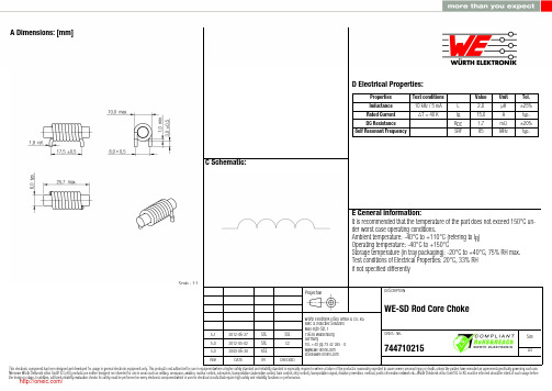
5.1 5.0 4.02012-06-272012-05-022009-06-30SStSStRStSStCZWürth Elektronik eiSos GmbH & Co. KGEMC & Inductive SolutionsMax-Eyth-Str. 174638 WaldenburgGermanyTel. +49 (0) 79 42 945 - 0A Dimensions: [mm]F Typical Impedance Characteristics:H4: Classification Wave Soldering Profile:H5: Classification Wave ProfileProfile FeaturePreheat- Temperature Min (T smin )- Temperature Typical (T stypical ) - Temperature Max (T smax ) - Time (t s ) from (T smin to T smax )Δ preheat to max Temperature Peak temperature (T p )Time of actual peak temperature (t p )Ramp-down rate - Min - Typical - MaxTime 25°C to 25°C Pb-Free Assembly 100°C 120°C 130°C 70 seconds 150°C max.250°C - 260°C max. 10 secondsmax. 5 second each wave ~ 2 K/s ~ 3.5 K/s ~ 5 K/s 4 minutesSn-Pb Assembly 100°C 120°C 130°C 70 seconds 150°C max.235°C - 260°C max. 10 secondsmax. 5 second each wave ~ 2 K/s ~ 3.5 K/s ~ 5 K/s 4 minutesrefer to EN 61760-1:2006H Soldering Specifications:I Cautions and Warnings:The following conditions apply to all goods within the product series of WE-SDof Würth Elektronik eiSos GmbH & Co. KG:General:All recommendations according to the general technical specifications of the data-sheet have to be complied with.The disposal and operation of the product within ambient conditions which probably alloy or harm the wire isolation has to be avoided.If the product is potted in customer applications, the potting material might shrink during and after hardening. Accordingly to this the product is exposed to the pressure of the potting material with the effect that the core, wire and termination is possibly damaged by this pressure and so the electrical as well as the mechanical characteristics are endanger to be affected. After the potting material is cured, the core, wire and termination of the product have to be checked if any reduced electrical or mechanical functions or destructions have occurred.The responsibility for the applicability of customer specific products and use in a particular customer design is always within the authority of the customer. All technical specifications for standard products do also apply for customer specific products.Washing varnish agent that is used during the production to clean the application might damage or change the characteristics of the wire in-sulation, the marking or the plating. The washing varnish agent could have a negative effect on the long turn function of the product.Direct mechanical impact to the product shall be prevented as the ferrite material of the core could flake or in the worst case it could break. Product specific:Follow all instructions mentioned in the datasheet, especially:•The solder profile has to be complied with according to the technical wave soldering specification, otherwise no warranty will be sustai-ned.•All products are supposed to be used before the end of the period of 12 months based on the product date-code, if not a 100% solderabi-lity can´t be warranted.•Violation of the technical product specifications such as exceeding the nominal rated current will result in the loss of warranty.1. General Customer ResponsibilitySome goods within the product range of Würth Elektronik eiSos GmbH & Co. KG contain statements regarding general suitability for certain application areas. These statements about suitability are based on our knowledge and experience of typical requirements concerning the are-as, serve as general guidance and cannot be estimated as binding statements about the suitability for a customer application. The responsibi-lity for the applicability and use in a particular customer design is always solely within the authority of the customer. Due to this fact it is up to the customer to evaluate, where appropriate to investigate and decide whether the device with the specific product characteristics described in the product specification is valid and suitable for the respective customer application or not.2. Customer Responsibility related to Specific, in particular Safety-Relevant ApplicationsIt has to be clearly pointed out that the possibility of a malfunction of electronic components or failure before the end of the usual lifetime can-not be completely eliminated in the current state of the art, even if the products are operated within the range of the specifications.In certain customer applications requiring a very high level of safety and especially in customer applications in which the malfunction or failure of an electronic component could endanger human life or health it must be ensured by most advanced technological aid of suitable design of the customer application that no injury or damage is caused to third parties in the event of malfunction or failure of an electronic component.3. Best Care and AttentionAny product-specific notes, warnings and cautions must be strictly observed.4. Customer Support for Product SpecificationsSome products within the product range may contain substances which are subject to restrictions in certain jurisdictions in order to serve spe-cific technical requirements. Necessary information is available on request. In this case the field sales engineer or the internal sales person in charge should be contacted who will be happy to support in this matter.5. Product R&DDue to constant product improvement product specifications may change from time to time. As a standard reporting procedure of the Product Change Notification (PCN) according to the JEDEC-Standard inform about minor and major changes. In case of further queries regarding the PCN, the field sales engineer or the internal sales person in charge should be contacted. The basic responsibility of the customer as per Secti-on 1 and 2 remains unaffected.6. Product Life CycleDue to technical progress and economical evaluation we also reserve the right to discontinue production and delivery of products. As a stan-dard reporting procedure of the Product Termination Notification (PTN) according to the JEDEC-Standard we will inform at an early stage about inevitable product discontinuance. According to this we cannot guarantee that all products within our product range will always be available. Therefore it needs to be verified with the field sales engineer or the internal sales person in charge about the current product availability ex-pectancy before or when the product for application design-in disposal is considered.The approach named above does not apply in the case of individual agreements deviating from the foregoing for customer-specific products.7. Property RightsAll the rights for contractual products produced by Würth Elektronik eiSos GmbH & Co. KG on the basis of ideas, development contracts as well as models or templates that are subject to copyright, patent or commercial protection supplied to the customer will remain with Würth Elektronik eiSos GmbH & Co. KG.8. General Terms and ConditionsUnless otherwise agreed in individual contracts, all orders are subject to the current version of the “General Terms and Conditions of Würth Elektronik eiSos Group”, last version available at .J Important Notes:The following conditions apply to all goods within the product range of Würth Elektronik eiSos GmbH & Co. KG:分销商库存信息: WURTH-ELECTRONICS 744710215。

信泓日佳销售产品目录表信泓日佳模具钢材公司销售模具钢,进口模具钢,高速钢,粉末高速钢,钨钢,铝材,铜材,铝板,铝棒如:日本:PX4 PX5 PDS-3 PDS-5 PAK90 PD555 PD613 SGT S50C SC5C SUS303 SUS304 SUS410 SUS420 SUS630 SCM440 SMC420 SUP9 SK3 SK4 SKD4 SKD5 SKD7 SKD8 SKD11 SKD12 SKD61 SKD62 SKH-9 SKH-51SKH-55 SKH57 SKH59 SKT4 SKS3 SKS41 SLD SLD8 SLD10 SM400A SNC815 SPHD SS41 SS330 SS400 SS490 S-Star GFA GOA GENA1 G-Star DAC DAC10 DAC45 DAC55 DEX20 DEX40 DEX60 DH21 DH31-S DH42 DH62 DHA DH2F DC11 DC53 DM FDAC YEM YEM-K YHD3 YHD27 YHD28 YHD45 YK30 YSS YXR3 YXR33 YXM1 YXM4 YXM42 MH51 MH85 NAK55 NAK80 NP8 NP9 ARK1 H3100 HAP10 HAP40 HAP72 HPM1 HPM2 HPM38 HPM50 HPM57 HPM77 化学成分瑞典:618S 618H 718 718S 718H S136 S136H 8407 8416 STAVAX ASP-23 ASP-30 UHB2311 RAMAX S ALVAR14 ASSAB88 DF3 DF2 ELMAX KM2 HMP41 HOTVAR V4 V10 ORO90 UHB20 UHB4006 UHB4462 UHB5752 UHB5860 UHB5919 UHB8159 UHB709 UHB8550 XW5 XW10 XW41 XW42 Q0R090化学成分奥国:A903 S500 S600 S709 S790 S705 S390PM S590PM S690PM M201 M202 M238 M261 M310 M238ESR W300 M330 M340 M461 W302 W303 W304 W321 W500 K100 K105 K110 K305 K340 K460 K600 K720 K990 VMRM300ESRM310ESR N100 N320 N540 N350 E116 E200 E220 E230 E400 F300 F530 V320 V155 V800 V820 化学成分德国:21NICRMO2 14NICR14 15CRNI6 20CRMO5 18CRNI8 55CR3 50CRV4 42CRMO4 34CRNIMO6 34CRALNI7 40CRNIMOA 638 2711 2316 2316H 2344 2379 2436 2510 2688 2738 1285 1292 2363 2767 2842 3207 1.3343 4125 1.7225 1.0037 1.1210 1.2101 1.1545 1.2080 1.2311 1.2312 1.2343 1.2365 1.2367 1.2550 1.2601 1.2606 1.2714 1.2840 1.2842 1.2885 1.3243 1.3247 1.3343 1.4006 1.4021 1.4034 1.4057 1.4313 1.4462 1.4542 1.4548 1.5752 1.5860 1.5919 1.6582 1.6523 1.7147 1.5920 1.7176 1.7225 1.7220 1.8509 1.8159中国:Cr12 Cr12MoV 6542 W18 W9 3Cr2W8V 15-40CrNiMo 15-42CrMo H13 20CrMnTi 30CrMnTi T8 T8A T10A T12 Y35CA Y12 Y15 Y20 Y30 Y40化学成分美国:P2 P3 P20 H11 H13 H10A F1 F2 F8 L2 L3 L6 M1 M2 M3 M4 M35 M42 M1008 M1020 W110 O1 O2 O6 L2 L3 T1 T15 S1 S7 D2 D3 D6 D7 A2 A3 A6 A8 A10 420 S7 1005 1018 1020 1035 1042 1050 1053 1069 1071 1086 1095 1018 13115 1513 1524 1548 1566 2024 2317 3135 3245 3450 4012 4024 4121 4130 4140 4150 4608 4715 4820 5015 5120 5052 5083 6061 6062 6115 6195 7055 7058 7072 7075 7260 8120 8620 8622 8742 9254 9260 A570.Gr.A K52440钨钢:G1 G2 G3 G4 G5 G6 G7 G8 G9 G10 G11 V30 V40 D30 D40 D50 D60 KE11 SF-05 SF-15 SF-20 SF-30 SF-X K05 K10 K20 YG8 YG9 YG12 YG15 YG20 YG25 YG28 CD650 CD636 CD750 化学成分高速钢:SKH-9 SKH-51 SKH-55 M2 M35 M42 ASP-23 ASP-30 V10 S600 S790铜料:日本三宝红铜银铜铜材紫铜杯士铜铬铜铍铜钨铜合金铜磷青铜锡青铜 C5191 C3604 C3600 C2801 C1100化学成分轧辊钢:9Cr2Mo 9Cr2MoV 718 P20不锈钢:301 302 303 304 310 316 401 410 420 430 440 630 1CR13 2CR13 3CR13 3CR13 4CR13 S31500 S31803 S31220 S36550 321铝板:6061-T651 50527075 8011 8005 8079 6056 6012 5086 2024 1200 1100 5050 1050化学成分易切削结构钢:15S10 1.0710 10S20 1.0721 15S20 15S22 1.0723 35S20 1.0726 45S20 46S20 1.0727 60S20 60S22 1.0728 10SPb20 1.0722 35SPb 1.0756 45SPb20 46SPb20 1.0757 60SPb20 60SPb22 1.0758 9SMn28 11SMn30 1.0736 9SMn36 11SMn37 1.0736 9SMnPb28 11SMnPb30 1.0718 9SMnPb36 11SMnPb37 1.0737 9S20 11SMn28 11SMnPb28 12SMnPb35 12SMn35 10Pb20 10SPb20 17SMn2035S20 35SMn20 44SmN28 46S20 …….冷镦钢和冷挤压钢:Cq15 C15C 1.1132 Cq22 C22C 1.1152 Cq35 C35C 1.1172 Cq45 C45C 1.1192 38Cr1 1.7001 46Cr1 1.7002 38Cr1 1.700 46Cr2 1.7006 15Cr3 1.7015 34Cr4 1.7033 37Cr4 1.7034 41Cr4 1.7035 25CrMo4 1.7218 34CrMo4 1.7220 42CrMo4 1.7225 20MoCr4 1.7321 16MnCr5 1.7131 15CrNi6 1.5919 30CrNiMo8 1.6580 34CrNiMo6 1.6582 20NiCrMo2-21 21NiCrMo2 1.6523 CC4X CC4A CC8S CC8A CC11X CC11A CE10 CE15E4 CE16E4 CE20E4 20CRE4 16MnCr5E 18MnCr4E 18CrMo4E 20NiMo2E CE20E4 CE28E4 CE35E4 CE40E4 CE45E4 42Mn6E 37Cr2E 46Cr2E 34Cr4E 37Cr4e 41Cr4E 41Cr4E 36Mo3E 25CrMo4e 34CrMo4e 42CrMo4e 41CrNiMo2E 41NiCrMo7E31CrNiMo8e CE20BG1 CE20BG2 CE28B CE35B 35MnB5E 37CrBLE …弹簧钢和轴承钢:C67ECK67 1.1231 C75E CK75 1.1248 C85E CK85 1.1269 C10E CK101 1.1274 38Si6 1.5022 38Si7 1.5023 46Si7 1.5024 51Si7 1.5025 55Si7 56Si7 1.5026 65Si7 1.5028 71Si7 1.5029 60SiMn5 1.5142 51MnV7 1.5225 54SiCr6 1.7102 60SiCr7 1.7108 67SiCr5 1.7103 55Cr3 1.7176 51CrC4 50CrV4 1.8159 58CrV4 1.8161 ......刀具用钢:SKS11 SKS2 SKS21 SKS5 SKS7 SKS81 SKS8 ……….耐冲击工具钢:SKS4 SKS41 SKS43 SKS44……….冷作模具钢:SKS3 SKS31 SKS93 SKS94 SKS95 SKD1 SKD2 SKD10 SKD12 SKD11 ……….热作模具钢:SKD4 SKD5 SKD6 SKD61 SKD62 SKD7 SKD8 SKT3 SKT4 SKT6…………)日本JIS标准结构钢牌号:SS330 SS400 SS490 SS540 SCM4400A SM400B SM400C SM490A SM490 SM490C SM490YA SM490YB SM570 CUP-Ten CUP-Ten60 FTW-52 FTW-60 FTW-70 HI-Z HI-Z Super HI-YAW-TEN HTP-52W NK-HITEN50 NK-HITE60 NK-HITEN70 NK-HITEN80 NK-HTEN100 RiverAce60 RiverAce70 RiverAce80 Welten50 Welten60 Welten70 Welten80 Welten80C Welten100N YAW-TEN50 Zirten SMA400AW SMA400BW SMA400CW SMA400AP SMA400BP SMA400CP SMA490AW SMA490BW SMA490CW SMA490AP SMA490BP SMA490CP SWA570W SWA570P SPA-H APA-C SPV315 SPV355 SPV410 SPV410 SPV450 SPV490 SPV235 SG255 SG295 SG325 SG365 SGV410 SGV450 SGV480 SGV42 SGV46 SGV49 SLA235A ALA235B ALA325B ALA325B ALA365 ALA410 SL2N255 SL3N255日本JIS标准机械结构用钢牌号:S10C S12C S15C S17C S20C S22C S25C S28C S30C S33C S35C S38C S40C S43C S45C S48C S50C S53C S58C S09CK S15CK S20CK日本JIS标准淬透性结构用钢牌号:SMn420H SMn433H SMn438H SMn4443H SCr415H SCr420H SCr435H SCr440HSCM415H SCM418H SCM420H SCM435H SCM440H SCM822H SNC415H SNC631H SNC220H SNC420H日本JIS标准易切削钢牌号:SUM11 SUN12 SUM21 SUM22 SUM22L SUM23 SUM23L SUM24L SUM25 SUM31 SUM31L SUM41 SUM42 SUM43 …………日本JIS标准合金钢牌号:SNB5 SNB7 SNB16 SNB21-1-5日本JIS标准轴承钢牌号:SUP3 SUP6 SUP7 SUP9 SUP9A AUP10 AUP11A AUP12 AUP13 SUJ1 SUJ2 SUJ3 SUJ4 SUJ5日本JIS标准不绣钢耐热钢牌号:SUS201 SUS202 SUS301 SUS302 SUS303 SUS303Se SUS303Cu SUS304 SUS304L SUS304N1 SUS304N2 SUS304LN SUS304J3 SUS305 SUS309S SUS309S SUS310S SUS316 SUS316L SUS316NSUS316LN SUS316F SUS317 SUS317L SUS317LN SUS317J1 SUS836L SUS890L SUS321 SUS347 SUSXM7 SUSXM15J1 SUS329J1 SUS329J1 SUS329J1 SUS329J4L SUS405 SUS410L SUS430 SUS430F SUS44J1 SUUSXM27 SUS403 SUS410 SUS410J1 SUS410F2 SUS416 SUS420J1 SUS420J2 SUS420F SUS420F2 SUS431 SUS440A SUS440F SUS630SUS631 SUS304TP SUS304HTP SUS309TP SUS310TP SUS890LTP SUS347HTP SUS304TKA SUS304TKC SUS316TKA SUS316TK SUS321TKA SUSTKC SUS420J1TKA SUS430TKA SUSTKC SUH31 SUH35 SUH36 SUH37 SUH38 SUH309 SUH310 SUH330 SUH660 SUH661 SUH446 SUH1 SUH3 SUH4 SUH11日本JIS标准高温合金钢耐蚀钢牌号:NCF600 NCF601 NCT625 NCF690 NCF718 NCF718 NCF750 NCF751 NCE800 NCF800H NCF825 NCF80A NCF600TP NCF600TB NCF625TP NCF800TP NCF825TP NCF825TB日本JIS标准工具钢牌号:SK140 SK120 SK105 SK95 SK90 SK85 SK80 SK75 SK70 SK65 SK60日本JIS标准高速钢牌号:SKH2 SKH3 SKH4 SKH10 SKH40 SKH50 SKH51 SKH52 SKH53 SKH54 SKH55 SKH56 SKH57 SKH58 SKH59………日本JIS标准特殊钢中空钢牌号:SK3M SK3M SK4M SK5M SK6M SK7M SK2M SK5M SKS51M SKS81MSKS95M SKC3 SKC11 SKC24 SKC25 SKC31日本JIS标准钨钢(硬质合金钢)牌号:切削工具用:P01 P15 P10 P20 P30 P40 M10 M20 M30 M40 K01 K10 K20 K30………拉丝模和顶尖工具用:V10 V20 V30……….矿山的质地工具用:,E1 E2 E4 E5………超微粒硬质合金:Z01 Z10 Z20 Z30 …………A1 A40 CC F0 F1 G2 G3 G5 G8 G10E H1 H2 H3 ST10E ST15E ST20E ST25E ST30E ST40E T12A T3S U1 U10E AC720 AC805 AC835………日本JIS标准结构用铸钢牌号:SC360 SC37 SC410 SC42 SC450 SC46 SC480 SC49 SC360 SC410 SC450 SC480 200-400 200-400W 230-450 230-450W 270-480W 340-550 340-550W SCW410 SCW42 SCW450 SCW46 SCW480 SCW49 SCW63SCC3 SCC5 SCMn1 SCMn2 SCMn3 SCMn5 SCMnCr2…….SCC3A SCC3B……….瑞典SS标准,碳素结构钢:1211 1225 1226 1232 1233 1234 1250 1265 1300 1310 1311 1312 1313 1330 1331 1332 1350 1357 1370 1410 1411 1412 1413 1414 1421 1422 1423 1424 1430 1431 1432 1434 1435 1450 1500 1510 1550 1550 1572 1600 1650 1655 1660 1665 1672 1674 1678合金结构钢:2085 2090 2101 2102 2103 2106 2107 2108 2110 2112 2114 2116 2117 2120 2121 2122 2127 2128 2130 2131 2132 2134 2135 2142 2143 2144 2145 2165 2168 2172 2173 2174 2203 2216 2218 2225 2228 2230 2231 2233 2243 2240 2244 2245 2253 2254 2258 2506 2511 2512 2520 2523 2530 2532 2534 2536 2541 2316 2615 2624 2625 2632 2634 2642 2644 2652 2654 2662 2664 2942 2940……弹簧钢: 1770 1774 1778…….易切削钢: 1912 1214 1922 1926 1940 1957 1973……..不绣钢和耐热钢:2301 2302 2303 2304 2317 2320 2321 2322 2323 2324 2325 2326 2327 2328 2331 2332 2333 2337 2338 2340 2343 2346 2347 2348 2350 2352 2353 2357 2360 2361 2366 2367 2368 2370 2371 2372 2374 7376 2377 2378 2380 2382 2383 2384 2387 2388 2562 2564 2570 2584 2662 2301-02 2301-22 2301-23 2302-02 2302-03 2303-02 2303-03 0303-04 2303-08 2304-02 2304-08 2317-03 2321-02 2321-03 2324-02 2325-02 2326-02 2326-22 2326-23 2326-26 2326-28 2340-04 2343-04 2343-22 2343-23 2343-24 2343-26 2343-27 2343-28 2343-29 2346-02 2346-02 2347-02 2347-22 2347-23 2347-26 2347-27 2347-28 2347-29 2348-02 2348-22 2348-23 2348-24 2348-25 2348-27 2348-28 2348-29 2350-02 2350-27 2350-28 2350-29 2352-02 2352-27 2352-29 2353-02 2353-28 2353-29 2366-27 2366-28 2366-29 2367-02 2367-28 2367-29 2370-02 2370-27 2370-28 2370-29 2371-02 2371-27 2371-29 2374-02 2374-27 2374-28 2374-29 2375-02 2380-02 2380-03 2570-03 2570-04 2570-04 2750-08 2375-27 2375-28 2375-29瑞典SS标准,碳素工具钢:1770 1778 1880 1885………..合金工具钢: 2092 2140 2242 2260 2310 2312 2314 2511 2514 2540 2550 2700 2705 2710 2730 2900 2940………高速工具钢:2715 2716 2722 2723 2724 2725 2736 2750 2752 2754 2756 2782 HSP-6 HSP-11 HSP-15 HSP-16 SHP-17 HSP41 HSP-42 ASP-23PM ASP-30PM ASP-60PM ASP-23 ASP-30 ASP-60….….工具钢及硬质合金钢:2726 2727 2736 2750 2752 2754 2756 2782 CG20 CG35 CG40 CG60 CN02 CN10 CN30 CN40 CS05 CS10 CS20 CS35 CT30 CT45 CT50 CT60 CT75 CT60 CT75 CT85 F02 H05 H10 H20 HIP HM HML RIP R4 S2 S4 S6 SIP SH SM …….涂层硬质合金:GC015 GC135 GC315 GC1025 PO5 P35 K05 K20 P25 P45 M15 M20 K05 K25 P10 P35 K20 ………..末涂层硬质合金:B1 B2 B23 B45 G4 G5 G27 K40 M40 H5 H13 K01 K10 H20 K20 H30 K30 H45 HX K10 K30 M10 M20 S1F P01 P15 S1G P01 P10 S2 P10 P20 S4 M20 P20 P30 S6 M30 P10 P40 S25M SU41 K10 K20 M10 M20 SecoticKSecticTP15 SecticTP25 Secotic TP35….非合金钢和合金钢牌号:1305 1306 1505 1606 2120 2133 2172 2183 2223 2224 2225………不绣耐蚀铸钢:2302 2324 2333 2343 2343-12 2366 2377 2385 2387 2564 2564……..瑞典灰铸铁:0110-00 0115-00 0125-00 0130-00 0140-00 215 217 219 221 223 ….球墨铸铁: 0717-00 0717-02 0717-15 0722-00 0727-02 0732-01 0772-00 0776-03 ….可锻铸铁: 0814-00 0815-00 0852-00 0854-00 0856-00 0862-03 0864-03……..经营美国“ALCOA”优质铝板、铝棒范围:6061-T6,7075-T651,A5052-H32,7075-T6,6061-T651,5052-H112,5086-H32,5083-H111,5083-H112,1100,1050,1 060 6063,5083,5086,2011,2017,2024,3003,7022,7050,7072,6060,6061,7075,5052等合金铝板/棒/管材等★经营国产优质铝板、铝棒范围:6061-T6,7075-T651,A5052-H32,7075-T6,6061-T651, 5083-H111, 1050,1060,6061,7075,5052,6063,5083, 5086,6062,6082-T6,6262,5154,5754,5356,3000,491,LY12,LC4,1XXX,7009等合金铝板/棒/管材等常备现货铝板/厚度如下:6061: 2mm-280mm; 7075: 2mm-180mm 5052: 1mm-80mm 5083: 8mm-80mm7075-T651: 10mm-180mm 6063: 2mm-280mm 2017: 4mm-80mm6061-T6: 3mm-280mm A5052-H32: 0.5mm-10mm 5083-H111: 1mm-10mm合金铸铁: 0457-00 0466-00 0512-00 0513-00 0747-03 0747-04 ……瑞典常用钢:618 618S 718 718S 718H S136 S136H 8407 8416 STAVAX UHB33 RAMAXS ALVAR14 ASSAB88 DF3 DF2 ELMAX KM2 HMP41 HOTVAR V4 V10 ORO90 UHB20 UHB4006 UHB4462 UHB5752 UHB5860 UHB5919 UHB8159 UHB709 UHB8550 ASP-23 ASP-30 ASP-60 ………….上海扩进模具材料有限公司大量销售模具钢,进口模具钢,高速钢,粉末高速钢,钨钢,铝材,铜材,铝板,铝棒如:日本 :PX4 PX5 PDS-3 PDS-5 PAK90 PD555 PD613 SGT S50C SC5C SUS303 SUS304 SUS410 SUS420 SUS630 SCM440 SMC420 SUP9 SK3 SK4 SKD4 SKD5 SKD7 SKD8 SKD11 SKD12 SKD61 SKD62 SKH-9 SKH-51 SKH-55SKH57 SKH59 SKT4 SKS3 SKS41 SLD SLD8 SLD10 SM400A SNC815 SPHD SS41 SS330 SS400 SS490 S-Star GFA GOA GENA1 G-Star DAC DAC10 DAC45 DAC55 DEX20 DEX40 DEX60 DH21 DH31-S DH42 DH62 DHA DH2F DC11 DC53 DM FDAC YEM YEM-K YHD3 YHD27 YHD28 YHD45 YK30 YSS YXR3 YXR33 YXM1 YXM4 YXM42 MH51 MH85 NAK55 NAK80 NP8 NP9 ARK1 H3100 HAP10 HAP40 HAP72 HPM1 HPM2 HPM38 HPM50 HPM57 HPM77 化学成分瑞典:618S 618H 718 718S 718H S136 S136H 8407 8416 STAVAX ASP-23 ASP-30 UHB2311 RAMAX S ALVAR14 ASSAB88 DF3 DF2 ELMAX KM2 HMP41 HOTVAR V4 V10 ORO90 UHB20 UHB4006 UHB4462 UHB5752 UHB5860 UHB5919 UHB8159 UHB709 UHB8550 XW5 XW10 XW41 XW42 Q0R090化学成分奥国:A903 S500 S600 S709 S790 S705 S390PM S590PM S690PM M201 M202 M238 M261 M310 M238ESR W300 M330 M340 M461 W302 W303 W304 W321 W500 K100 K105 K110 K305 K340 K460 K600 K720 K990 VMRM300ESRM310ESR N100 N320 N540 N350 E116 E200 E220 E230 E400 F300 F530 V320 V155 V800 V820 化学成分德国:21NICRMO2 14NICR14 15CRNI6 20CRMO5 18CRNI8 55CR3 50CRV4 42CRMO4 34CRNIMO6 34CRALNI7 40CRNIMOA 638 2711 2316 2316H 2344 2379 2436 2510 2688 2738 1285 1292 2363 2767 2842 3207 1.3343 4125 1.7225 1.0037 1.1210 1.2101 1.1545 1.2080 1.2311 1.2312 1.2343 1.2365 1.2367 1.2550 1.2601 1.2606 1.2714 1.2840 1.2842 1.2885 1.3243 1.3247 1.3343 1.4006 1.4021 1.4034 1.4057 1.4313 1.4462 1.4542 1.4548 1.5752 1.5860 1.5919 1.6582 1.6523 1.7147 1.5920 1.7176 1.7225 1.7220 1.8509 1.8159中国:Cr12 Cr12MoV 6542 W18 W9 3Cr2W8V 15-40CrNiMo 15-42CrMo H13 20CrMnTi 30CrMnTi T8 T8A T10A T12 Y35CA Y12 Y15 Y20 Y30 Y40化学成分美国:P2 P3 P20 H11 H13 H10A F1 F2 F8 L2 L3 L6 M1 M2 M3 M4 M35 M42 M1008 M1020 W110 O1 O2 O6 L2 L3 T1 T15 S1 S7 D2 D3 D6 D7 A2 A3 A6 A8 A10 420 S7 1005 1018 1020 1035 1042 1050 1053 1069 1071 1086 1095 1018 13115 1513 1524 1548 1566 2024 2317 3135 3245 3450 4012 4024 4121 4130 4140 4150 4608 4715 4820 5015 5120 5052 5083 6061 6062 6115 6195 7055 7058 7072 7075 7260 8120 8620 8622 8742 9254 9260 A570.Gr.A K52440钨钢如:G1 G2 G3 G4 G5 G6 G7 G8 G9 G10 G11 V30 V40 D30 D40 D50 D60 KE11 SF-05 SF-15 SF-20 SF-30 SF-X K05 K10 K20 YG8 YG9 YG12 YG15 YG20 YG25 YG28 CD650 CD636 CD750 化学成分高速钢:SKH-9 SKH-51 SKH-55 M2 M35 M42 ASP-23 ASP-30 V10 S600 S790铜料如:日本三宝红铜银铜铜材紫铜杯士铜铬铜铍铜钨铜合金铜磷青铜锡青铜 C5191 C3604C3600 C2801 C1100化学成分轧辊钢:9Cr2Mo 9Cr2MoV 718 P20不锈钢:301 302 303 304 310 316 401 410 420 430 440 630 1CR13 2CR13 3CR13 3CR13 4CR13 S31500 S31803 S31220 S36550 321铝板:6061-T651 50527075 8011 8005 8079 6056 6012 5086 2024 1200 1100 5050 1050化学成分易切削结构钢:15S10 1.0710 10S20 1.0721 15S20 15S22 1.0723 35S20 1.0726 45S20 46S20 1.0727 60S20 60S22 1.0728 10SPb20 1.0722 35SPb 1.0756 45SPb20 46SPb20 1.0757 60SPb20 60SPb22 1.0758 9SMn28 11SMn30 1.0736 9SMn36 11SMn37 1.0736 9SMnPb28 11SMnPb30 1.0718 9SMnPb36 11SMnPb37 1.0737 9S20 11SMn28 11SMnPb28 12SMnPb35 12SMn35 10Pb20 10SPb20 17SMn2035S20 35SMn20 44SmN28 46S20 …….冷镦钢和冷挤压钢:Cq15 C15C 1.1132 Cq22 C22C 1.1152 Cq35 C35C 1.1172 Cq45 C45C 1.1192 38Cr1 1.7001 46Cr1 1.7002 38Cr1 1.700 46Cr2 1.7006 15Cr3 1.7015 34Cr4 1.7033 37Cr4 1.7034 41Cr4 1.7035 25CrMo4 1.7218 34CrMo4 1.7220 42CrMo4 1.7225 20MoCr4 1.7321 16MnCr5 1.7131 15CrNi6 1.5919 30CrNiMo8 1.6580 34CrNiMo6 1.6582 20NiCrMo2-21 21NiCrMo2 1.6523 CC4X CC4A CC8S CC8A CC11X CC11A CE10 CE15E4 CE16E4 CE20E4 20CRE4 16MnCr5E 18MnCr4E 18CrMo4E 20NiMo2E CE20E4 CE28E4 CE35E4 CE40E4 CE45E4 42Mn6E 37Cr2E 46Cr2E 34Cr4E 37Cr4e 41Cr4E 41Cr4E 36Mo3E 25CrMo4e 34CrMo4e 42CrMo4e 41CrNiMo2E 41NiCrMo7E31CrNiMo8e CE20BG1 CE20BG2 CE28B CE35B 35MnB5E 37CrBLE …..弹簧钢和轴承钢:C67ECK67 1.1231 C75E CK75 1.1248 C85E CK85 1.1269 C10E CK101 1.1274 38Si6 1.5022 38Si7 1.5023 46Si7 1.5024 51Si7 1.5025 55Si7 56Si7 1.5026 65Si7 1.5028 71Si7 1.5029 60SiMn5 1.5142 51MnV7 1.5225 54SiCr6 1.7102 60SiCr7 1.7108 67SiCr5 1.7103 55Cr3 1.7176 51CrC4 50CrV4 1.8159 58CrV4 1.8161 ......刀具用钢:SKS11 SKS2 SKS21 SKS5 SKS7 SKS81 SKS8 ……….耐冲击工具钢:SKS4 SKS41 SKS43 SKS44……….冷作模具钢:SKS3 SKS31 SKS93 SKS94 SKS95 SKD1 SKD2 SKD10 SKD12 SKD11 ……….热作模具钢:SKD4 SKD5 SKD6 SKD61 SKD62 SKD7 SKD8 SKT3 SKT4 SKT6…………)日本JIS标准结构钢牌号:SS330 SS400 SS490 SS540 SCM4400A SM400B SM400C SM490A SM490 SM490C SM490YA SM490YB SM570 CUP-Ten CUP-Ten60 FTW-52 FTW-60 FTW-70 HI-Z HI-Z Super HI-YAW-TEN HTP-52W NK-HITEN50 NK-HITE60 NK-HITEN70 NK-HITEN80 NK-HTEN100 RiverAce60 RiverAce70 RiverAce80 Welten50 Welten60 Welten70 Welten80 Welten80C Welten100N YAW-TEN50 Zirten SMA400AW SMA400BW SMA400CW SMA400AP SMA400BP SMA400CP SMA490AW SMA490BW SMA490CW SMA490AP SMA490BP SMA490CP SWA570W SWA570P SPA-H APA-C SPV315 SPV355 SPV410 SPV410 SPV450 SPV490 SPV235 SG255 SG295 SG325 SG365 SGV410 SGV450 SGV480 SGV42 SGV46 SGV49 SLA235A ALA235B ALA325B ALA325B ALA365 ALA410 SL2N255 SL3N255日本JIS标准机械结构用钢牌号:S10C S12C S15C S17C S20C S22C S25C S28C S30C S33C S35C S38C S40C S43C S45C S48C S50C S53C S58C S09CK S15CK S20CK日本JIS标准淬透性结构用钢牌号:SMn420H SMn433H SMn438H SMn4443H SCr415H SCr420H SCr435H SCr440H SCM415H SCM418H SCM420H SCM435H SCM440H SCM822H SNC415H SNC631H SNC220H SNC420H日本JIS标准易切削钢牌号:SUM11 SUN12 SUM21 SUM22 SUM22L SUM23 SUM23L SUM24L SUM25 SUM31 SUM31L SUM41 SUM42 SUM43 …………日本JIS标准合金钢牌号:SNB5 SNB7 SNB16 SNB21-1-5日本JIS标准轴承钢牌号:SUP3 SUP6 SUP7 SUP9 SUP9A AUP10 AUP11A AUP12 AUP13 SUJ1 SUJ2 SUJ3 SUJ4 SUJ5日本JIS标准不绣钢耐热钢牌号:SUS201 SUS202 SUS301 SUS302 SUS303 SUS303Se SUS303Cu SUS304 SUS304L SUS304N1 SUS304N2 SUS304LN SUS304J3 SUS305 SUS309S SUS309S SUS310S SUS316 SUS316L SUS316NSUS316LN SUS316F SUS317 SUS317L SUS317LN SUS317J1 SUS836L SUS890L SUS321 SUS347 SUSXM7 SUSXM15J1 SUS329J1 SUS329J1 SUS329J1 SUS329J4L SUS405 SUS410L SUS430 SUS430F SUS44J1 SUUSXM27 SUS403 SUS410 SUS410J1 SUS410F2 SUS416 SUS420J1 SUS420J2 SUS420F SUS420F2 SUS431 SUS440A SUS440F SUS630SUS631 SUS304TP SUS304HTP SUS309TP SUS310TP SUS890LTP SUS347HTP SUS304TKA SUS304TKC SUS316TKA SUS316T SUS321TKA SUSTKC SUS420J1TKA SUS430TKA SUSTKC SUH31 SUH35 SUH36 SUH37 SUH38 SUH309 SUH310 SUH330 SUH660 SUH661 SUH446 SUH1 SUH3 SUH4 SUH11日本JIS标准高温合金钢耐蚀钢牌号:NCF600 NCF601 NCT625 NCF690 NCF718 NCF718 NCF750 NCF751 NCE800 NCF800H NCF825 NCF80A NCF600TP NCF600TB NCF625TP NCF800TP NCF825TP NCF825TB日本JIS标准工具钢牌号:SK140 SK120 SK105 SK95 SK90 SK85 SK80 SK75 SK70 SK65 SK60日本JIS标准高速钢牌号:SKH2 SKH3 SKH4 SKH10 SKH40 SKH50 SKH51 SKH52 SKH53 SKH54 SKH55 SKH56 SKH57 SKH58 SKH59………..日本JIS标准特殊钢中空钢牌号:SK3M SK3M SK4M SK5M SK6M SK7M SK2M SK5M SKS51M SKS81MSKS95M SKC3 SKC11 SKC24 SKC25 SKC31日本JIS标准钨钢(硬质合金钢)牌号:切削工具用:P01 P15 P10 P20 P30 P40 M10 M20 M30 M40 K01 K10 K20 K30。


UTPDescriptionFull plastic circular connector with rugged plastic bayonet coupling system RangeShell sizes: 8Contact arrangements: 10 (3 to 48)FeaturesDerived from MIL - C 26482Intermateable with UTO / UTG IP65 (waterprotected version)Min 250 matings/unmatings 2 VDE versionsAccessoriesDifferent type of cable clamps DustcapsDiscrimination pinsUTGDescriptionPlastic circular connector with metal bayonet coupling system RangeShell sizes: 8Contact arrangements: 11 (3 to 48)FeaturesDerived from MIL - C 26482Intermateable with UTO / UTP IP65 (waterprotected version)Min 500 matings/unmatings 3 VDE versionsAccessoriesDifferent types of cable clamps DustcapsDiscrimination pinsUTODescriptionMetal circular connector with metal bayonet coupling system RangeShell sizes: 8Contact arrangements:8 (4 to 48)Features (see also page 2)Derived from MIL - C 26482Intermateable with UTG / UTP 2 levels of water protection:Dynamic IP67/IP69K and IP68/IP69K Suitable for EMC requirements Min 500 matings/unmatings2 levels of salt spray: 48 and 96hHigher salt spray (200/500h) upon request Cat5e ethernet compatibleBack shells with metric cable glands RoHS compliantAccessoriesDifferent types of cable clamps Shielded cable clamp DustcapsMBGDescriptionPlastic circular connector with metal quick mating feature (push-pull)RangeShell sizes: 5Contact arrangements:5 (4 to 46)FeaturesMin 5000 matings/unmatingsQuick and easy mating with latching system Accessories Cable clampn e wMS-M MSOV35 - DTE/DCEDescriptionHigh performance rectangular cable connector RangeShell sizes: 9Contact arrangements: 9 to 75FeaturesPer MIL - C 28748 Intermateable with MSO AccessoriesDifferent types of cable clamps Guide and jackscrew pins Pin protection shrouds Discrimination pinsDescriptionRectangular boardmount connector to mate with MS-M cable connectors RangeShell sizes:5Contact arrangements: 5 straight (9 to 75)3 right angle (9,18,34)FeaturesSolid machined or stamped and formed contacts Intermateable with MS-M AccessoriesGuide and jackscrew pinsDiscrimination pinsDescriptionRectangular cable and boardmount connector for V .35 DTE/DCE interface applicationsRange1 shell size with 34 contact positionsstraight and right angle boardmount connector FeaturesIn compliance with international standards of ISO 2593 for TSS V .35 interfacingSolid machined or stamped and formed contacts for boardmount connectorShielded cable and boardmount connectors availableAccessoriesDifferent type of cable clamps (incl. shielded) Guide and jackscrew pinsPin protection shrouds and discrimination pinsSMS - Qikmate cable connectors SMS - Qikmate boardmountDescriptionLow cost rectangular cable connectors for cable to cable and cable to panel applications RangeShell sizes: 10Contact arrangements:10 (2 to 36)FeaturesIntermateable with SMS Boardmount Moulded-on cable hood No extra hardware requiredPositive locking with retaining latchesDisrrimination cavities in between contact cavities AccessoriesPin protection shrouds Discrimination pins Tie wrapsDescriptionLow cost rectangular boardmount connector to mate with SMS cable connectors RangeShell sizes:10Contact arrangements: 10 straight (2 to 36)4 right angle (3,6,12,18)FeaturesSolid machined or stamped and formed contacts No extra hardware requiredIntermateable with SMS cable connectorsDisrrimination cavities in between contact cavities AccessoriesDiscrimination pinsMSG / MBDescriptionCable (MSG + MB) and boardmount (MSG) connectors with lever locking system.RangeShell sizes: 1 for MSG 1 for MB Contact arrangements: 50 + 59 for MSG 52 for MB FeaturesLever locking system – easy mating MSG is 19” rack mountable Polarization features available Anti jack knife system on MBn e wRM/RC-M (size 16)DescriptionMachined Snap in pin and socket contacts for heavy duty top performance requirements. Range30 to 14 AWG – 0.05 to 2.5 mm2Crimp, PC Boardmount, HandsolderWire wrap, Grounding contactsFeaturesCurrent rating: 13 AmpsPlating: Gold or TinColour coded for different wire sizesSM/SC-M (size 16)DescriptionTwo piece strip formed snap in pin and socketcontacts.Range26 to 14 AWG – 0.13 to 2.0 mm2Crimp.FeaturesCurrent rating: 13 AmpsPlating: Gold or TinRMDX/RCDX (size 16)DescriptionSnap in pin and socket coaxial contacts for a widerange of coaxial and twisted pair cables.RangeMulti piece or Monocrimp design.Typical coaxial cables are: RG161, RG178, RG179.RG188.FeaturesPlating: GoldFibre optic (size 16)DescriptionSnap in pin and socket fibre optic contacts for theintegration of optical links.RangePlastic optical Fibre (POF):1mm core and 2.2mm jacket.Plastic clad Fibre (PCF):230 µm core and 2.2 mm jacketMultimode Silica Fibre:50/125 µm type 1.5mm (or 900 µm) jacket.FeaturesSocket contact is spring loaded to avoid any airgap between the optical faces.RM/RC-W (size 20)DescriptionMachined Snap in pin and socket contacts for heavy duty top performance requirements. Range26 to 18 AWG – 0.13 to 1.0 mm2Crimp and PC BoardmountFeaturesCurrent rating: 7.5 AmpsPlating: Gold SM/SC-W (size 20)DescriptionTwo piece strip formed snap in pin and socket contacts.Range26 to 20 AWG – 0.13 to 0.5 mm2Crimp.FeaturesCurrent rating: 5 AmpsPlating: GoldUTOWDescriptionMetal circular connector with metal bayonet coupling system.RangeShell sizes: 8Contact arrangements: 8 (6 to 61) Features (see also page 2)2 levels of water protection:Dynamic IP67/IP69K and IP68/IP69KSuitable for EMC requirementsMin 500 matings/unmatings2 levels of salt spray: 48 and 96hHigher salt spray (200/500h) upon request Back shells with metric cable glandsRoHS compliantAccessoriesDifferent types of cable clampsShielded cable clampDustcapsDiscrimination pinsn e wUTV seriesDescriptionRuggedized metal circular connector for heavy duty applicationsRangeShell sizes: 8Contacts arrangements: 9 (7 to 60)FeaturesCompletely intermountable with VG95237: the MS5015 reverse bayonet connectors.2 levels of waterprotection:Dynamic IP67/69K and IP68/69K Up to 500 h salt spray.AccessoriesStraight back shells Right angle back shells Grommets and filler plugsCircular & Rectangular power versionsDescriptionPower connectors are connectors to meet mixed power / signal requirements.This range of power connectors is an extension of the long established and popular TRIM TRIO connector series8291 (power)DescriptionMachined snap in pin and sockets contacts for power applicationsRange Size 12 contacts: 20 to 14 AWG – 0.5 to 2.5 mm 2Size 8 contacts:16 to 8 AWG – 1.5 to 10 mm 2FeaturesCurrent rating: 26 Amps for size 12 contacts44 Amps for size 8 contactsPlating: Gold or Silver for size 12 contactsGold for size 8 contactsn e w分销商库存信息:SOURIAU-CONNECTIONSMS6P1SMS12R-1SMS12P-1 SMS6R1SMS9R1SMS2R1SMS2P1SMS9P1SMS24R-1 SMS36R-1SMS9PDH1SMS3PDH1 SMS12PDH1SMS36PDH1SMS12RDH1 SMS3P1SMS3R1SMS4R1SMS24P-1SMS18P1SMS36P-1 SMS2PDH1SMS4PDH1SMS6PDH1 SMS24PDH1SMS9RDH1SMS15PDH1 SMS6RDH1SMS24RDH1SMS18R1 SMS4P1SMS15R1SMS15P1 SMS18PDH1SMS2RDH1SMS3RDH1 SMS4RDH1SMS18RDH1SMS15RDH1 SMS36RDH1UTG12AC UTG14AC UTG18-AC UTG20AC UTG10PG UTG18PG UTG24PG UTG10AC UTG16AC UTG12PG UTG14PG UTG20PG UT014JCS UT018ACUT024AC UT016JC UT018JCL UTG22AC UTG16PG UTG22PGUT010JCS UT010AC UT012ACUT014AC UT012JCS SM20M-1TK6 SM14M1TK6SM24M1TK6SM16M1TK6 SM20W-3S26SM24W-3S26SC16M1TK6 SC24M1TK6SC14M1TK6SC20W-3S25 SC24W-3S25SM16ML-1TK6SM20M-1S6 SM24M-1S6SM14M-1S6SM16M-1S6 SC16ML-1TK6SC20ML-1TK6SC16M-1S6 SC14M-1S6SC24M-1S6SC20M-1S6 SC24WL-3S25SM24WL-3S26SM24WL-3TK6 SM20WL-3TK6SC24WL-3TK6SC20WL-3TK6 SM14ML-1S6SM16ML-1S6SC14ML-1S6 SC16ML-1S6SC20ML-1S6RC20M12D28 RM16M23D28RM20M12D2882911684ZX RM12Z43D2882911685NZX RC12Z43D28 SC20M-1TK6SM14ML-1TK6SM24ML-1TK6 SC24ML-1TK6SC14ML-1TK6SM20WL-3S26 SC20WL-3S25SM24ML-1S6SM20ML-1S6 SC24ML-1S6RC16M23D28SM20ML-1TK6 UTP01412S UTP0104S UTP0104P UTP0128S UTP0128P UTG01619S UTP01619P UTG014-12S UTG612-8PN UTP02448S UTG614-12PN UT001412SH。

Series CWMiniature Power RockersB12I n d i c a t o r sA c c e s s o r i e sS u p p l e m e n tT a c t i l e sK e y l o c k sR o t a r i e sP u s h b u t t o n sI l l u m i n a t e d P BS l i d e s P r o g r a m m a b l eT o u c hT i l tT o g g l e sGeneral SpecificationsElectrical CapacityPower Level: For Resistive Load 6A @ 250V ACOther RatingsContact Resistance: 20 milliohms maximumInsulation Resistance: 500 megohms minimum @ 500V DCDielectric Strength: 1,500V AC minimum between contacts for 1 minute minimum3,000V AC minimum between contacts & case for 1 minute minimum Mechanical Life: 30,000 operations minimumElectrical Life: 10,000 operations minimum with Resistive Load & 6,000 operations with Inductive Load N ominal Operating Force: 2.50N Angle of Throw: 30° Operating Temperature Range: –10°C ~ +70°C (+14°F ~ +158°F)Materials & FinishesRocker: Polycarbonate Stationary Contacts:Silver alloyHousing:PolyamideBase:Laminated thermosetting sheets Movable Contactor: Brass w/silver alloy plating Contact Terminals: Copper with silver platingMovable Contacts:SilverCommon Terminals:Brass with silver platingElectrical CapacityPower Level: For Resistive Load 6A @ 250V ACOther RatingsContact Resistance:20 milliohms maximumInsulation Resistance: 500 megohms minimum @ 500V DCDielectric Strength: 1,500V AC minimum between contacts for 1 minute minimum3,000V AC minimum between contacts & case for 1 minute minimum Mechanical Life: 30,000 operations minimumElectrical Life: 10,000 operations minimum with Resistive Load & 6,000 operations with Inductive Load N ominal Operating Force: 6.50N for single pole models; 10.0N for double pole models Angle of Throw: 30° Operating Temperature Range: –10°C ~ +70°C (+14°F ~ +158°F)Materials & FinishesRocker: Polycarbonate Stationary Contacts: Silver alloy Housing:Polyamide Base: Laminated thermosetting sheets Movable Contactor: Beryllium copper w/silver alloy plating Terminals: Brass with silver platingMovable Contacts:SilverElectrical CapacityPower Level: For Resistive Load 6A @ 125V AC; 3A @ 250V AC; 4A @ 30V DCOther RatingsContact Resistance:20 milliohms maximumInsulation Resistance: 1,000 megohms minimum @ 500V DCDielectric Strength: 1,000V AC minimum between contacts for 1 minute minimum1,500V AC minimum between contacts & case for 1 minute minimum Mechanical Life: 50,000 operations minimum Electrical Life: 25,000 operations minimum N ominal Operating Force: 2.0N Angle of Throw:30° Operating Temperature Range: –25°C ~ +70°C (–13°F ~ +158°F)Materials & FinishesRocker: Glass fiber reinforced polyamide Base: LCP (Liquid Crystal Polymer) Housing:Polyamide Contact Terminals: Brass + silver with silver plating Movable Contactor: Phosphor bronze w/silver plating Common Terminals: Brass with silver platingMovable Contacts:Silver alloyCWSB CWT CWSA/Series CWMiniature Power Rockers B13I n d i c a t o r s A c c e s s o r i e s S u p p l e m e n t T a c t i l e s K e y l o c k s R o t a r i e s P u s h b u t t o n s I l l u m i n a t e d P B S l i d e s P r o g r a m m a b l e T o g g l esT o u c h T i lt Distinctive CharacteristicsCWSALow cost molded rocker.See-saw contact mechanismStable stationary contact construction for high reliability.Easily installed with snap-in mounting.Large terminal hole dimensioned .067” x .098” (1.7mm x 2.5mm) simplifies wiring and soldering.Wave Soldering (PC version): See Profile A in Supplement section. Manual Soldering: See Profile A in Supplement section.CWSBLow cost molded rocker.Snap-acting contact mechanism gives smooth actuation and audible feedback.Stable stationary contact construction for high reliability.Front panel, snap-in mounting for labor-saving installation.Solder lug/quick connect terminals can be used with connectors.Manual Soldering: See Profile B in Supplement section.CWTLow cost molded rocker in compact, slim design.See-saw contact mechanismOutstanding insulation resistance and dielectric strength.Dust proof construction protects contact area.Stable stationary contact construction for high reliability.Front panel, snap-in mounting for labor-saving installation.Terminals are molded in and epoxy sealed to lock out flux, dust, and other contaminants.Manual Soldering: See Profile A in Supplement section./Series CWMiniature Power RockersB14I n d i c a t o r sA c c e s s o r i e s S u p p l e m e n tT a c t i l e sK e y l o c k sR o t a r i e sP u s h b u t t o n sI l l u m i n a t e d P B S l i d e sP r o g r a m m a b l eT o u c h T i l t T o g g l e sSTANDARDS & CERTIFICATIONSCWSASpecific CWSA models listed below are qualified for Underwriters Laboratories Inc. recognition and Canadian Standards Association certification. cULus marking on case is standard as noted in following table.Model Ratings @ AC cULus File No. Marking on CaseCWSA11 6A @ 250V E44145 StandardCWSA126A @ 250VE44145StandardCWSBSpecific CWSB models listed below are qualified for Underwriters Laboratories Inc. recognition and Canadian Standards Association certification. cULus marking on case is standard as noted in following table.Model Ratings @ AC cULus File No. Marking on CaseCWSB11 6A @ 250V E44145 StandardCWSB216A @ 250VE44145StandardCWTSpecific CWT model listed below is qualified for Underwriters Laboratories Inc. recognition and Canadian Standards Association certification. cULus marking on case is standard as noted in following table.Model Ratings @ AC cULus File No. Marking on CaseCWT126A @ 125V E44145Standard3A @ 250V/Series CWMiniature Power RockersB15I n d i c a t o r sA c c e s s o r i e s S u p p l e m e n t T a c t i l e s K e y l o c k s R o t a r i e s P u s h b u t t o n s I l l u m i n a t e d P BS l i d e s P r o g r a m m a b l e T o g g l esT o u c hT i ltTYPICAL ORDERING EXAMPLECWSA11AANSTYPICAL SWITCH ORDERING EXAMPLESFor SPST & SPDTNo CodeNoneFor SPST 1Horizontal 2Vertical 3Dot MarkingTYPICAL ORDERING EXAMPLECWSB21AA2FCWT12AAS1* Wire harness & cable assemblies offered only in Americas* Wire harness & cable assemblies offered only in Americas* Wire harness & cable assemblies offered only in Americas/Series CWMiniature Power RockersB16I n d i c a t o r s A c c e s s o r i e sS u p p l e m e n tT a c t i l e sK e y l o c k sR o t a r i e s P u s h b u t t o n sI l l u m i n a t e d P B S l i d e sP r o g r a m m a b l eT o u c hT i l t T o g g l e sTYPICAL SWITCH DIMENSIONS FOR CWSACWSA12AANSRight Angle Single Pole • Horizontal On-Off InscriptionSolder LugSingle Pole • No InscriptionCWSA11AAN1HINSCRIPTIONSNoneNot available in double pole.No CodeHorizontal OrientationOnly On-None-Off models are available with the horizontal inscription.1Vertical OrientationOnly On-None-Off models are available with the vertical inscription.2Dot MarkingOnly Single Pole On-None-Off models are available with the dot inscription.3The IEC symbols for On-Off are supplied with Single Throw models only. Orientation of inscription must be selected.Inscription color is white ink on black.Panel Thickness .030” ~ .079” (0.75mm ~ 2.0mm)Terminal numbers are on side of switch body Terminal numbers areon side of switch bodySingle throw model doesnot have terminal 1b /Series CWMiniature Power RockersB17I n d i c a t o r s A c c e s s o r i e s S u p p l e m e n tT a c t i l e sK e y l o c k sR o t a r i e sP u s h b u t t o n sI l l u m i n a t e d P B S l i d e sP r o g r a m m a b l e T o g g l esT o u c hT i l tCWT12AAS1Single Pole • No InscriptionSolder LugTYPICAL SWITCH DIMENSIONS FOR CWSBCWSB21AA2FSingle Pole • Dot Inscription Right AngleDouble Pole • Vertical On-Off InscriptionQuick ConnectCWSB11AA3HFootprint DPSTPanel Thickness .030” ~ .079” (0.75mm ~ 2.0mm)TYPICAL SWITCH DIMENSIONS FOR CWTPanel Thickness .030” ~ .079” (0.75mm ~ 2.0mm)FootprintSPSTTerminal numbers are on bottom of switchTerminal numbers are on bottom of switchTerminal numbers are on side of switch body /分销商库存信息:NKK-SWITCHCWSB11AA2F CWSB21AA1F CWSB21AA2F CWSA11AANS CWSA11AAN1S CWSA11AAN2S CWSA11AAN3S CWSB11AAF CWSA12AANS CWT12AAS1CWSA11AAN1H CWSB11AA1F CWSB11AA3F CWT12AAS1/U CWSA12AANH CWSA11AANH CWSB11AAH CWSA11AAN2H CWSB11AA1H CWT12AAS1/UC CWSB11AA3H CWSB21AA1H CWSB21AA2H。